![[Seminar5] Synch Netw](https://static.fdocuments.in/doc/165x107/55cf8dec550346703b8caeb2/seminar5-synch-netw.jpg)
LM2742 N-Chan FET Synch Buck Reg Cntrlr for Low Output ...
33
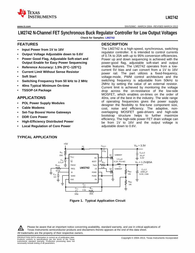
LM2742 HG BOOT I SEN LG PGND FB V CC SD PWGD FREQ SS SGND EAO PGND +5V V IN = 3.3V V O = 1.2V@5A CO1,2 2200 PF 6.3V, 2.8A 1.5 PH 6.1A, 9.6 m: R fb2 CC2 RC1 RCS CSS RFADJ RIN CIN D1 CBOOT Q1 Q2 10 PF 6.3V 10k 2.2k 10k 392k 2.2p 180p 12n 63.4k 2.2 PF 10: 0.1P CIN1,2 L1 + CC1 R fb1 Si4884DY Si4884DY LM2742 www.ti.com SNVS266C – MARCH 2004 – REVISED MARCH 2013 LM2742 N-Channel FET Synchronous Buck Regulator Controller for Low Output Voltages Check for Samples: LM2742 1FEATURES DESCRIPTION The LM2742 is a high-speed, synchronous, switching 2• Input Power from 1V to 16V regulator controller. It is intended to control currents • Output Voltage Adjustable down to 0.6V of 0.7A to 20A with up to 95% conversion efficiencies. • Power Good Flag, Adjustable Soft-start and Power up and down sequencing is achieved with the Output Enable for Easy Power Sequencing power-good flag, adjustable soft-start and output enable features. The LM2742 operates from a low- • Reference Accuracy: 1.5% (0°C–125°C) current 5V bias and can convert from a 1V to 16V • Current Limit Without Sense Resistor power rail. The part utilizes a fixed-frequency, • Soft Start voltage-mode, PWM control architecture and the switching frequency is adjustable from 50kHz to • Switching Frequency from 50 kHz to 2 MHz 2MHz by setting the value of an external resistor. • 40ns Typical Minimum On-time Current limit is achieved by monitoring the voltage • TSSOP-14 Package drop across the on-resistance of the low-side MOSFET, which enables on-times on the order of APPLICATIONS 40ns, one of the best in the industry. The wide range of operating frequencies gives the power supply • POL Power Supply Modules designer the flexibility to fine-tune component size, • Cable Modems cost, noise and efficiency. The adaptive, non- overlapping MOSFET gate-drivers and high-side • Set-Top Boxes/ Home Gateways bootstrap structure helps to further maximize • DDR Core Power efficiency. The high-side power FET drain voltage can • High-Efficiency Distributed Power be from 1V to 16V and the output voltage is adjustable down to 0.6V. • Local Regulation of Core Power TYPICAL APPLICATION Figure 1. Typical Application Circuit 1 Please be aware that an important notice concerning availability, standard warranty, and use in critical applications of Texas Instruments semiconductor products and disclaimers thereto appears at the end of this data sheet. 2All trademarks are the property of their respective owners. PRODUCTION DATA information is current as of publication date. Copyright © 2004–2013, Texas Instruments Incorporated Products conform to specifications per the terms of the Texas Instruments standard warranty. Production processing does not necessarily include testing of all parameters.
Transcript of LM2742 N-Chan FET Synch Buck Reg Cntrlr for Low Output ...
LM2742
HG
BOOT
ISEN
LG
PGND
FB
VCC
SD
PWGD
FREQ
SS
SGND
EAO
PGND
+5VVIN = 3.3V
VO = 1.2V@5A
CO1,2 2200 PF
6.3V, 2.8A
1.5 PH6.1A, 9.6 m:
Rfb2
CC2 RC1
RCS
CSS
RFADJ
RIN
CIN
D1 CBOOT
Q1
Q2
10 PF6.3V
10k
2.2k
10k
392k
2.2p
180p
12n
63.4k
2.2 PF
10:
0.1PCIN1,2
L1
+
CC1
Rfb1
Si4884DY
Si4884DY
LM2742
www.ti.com SNVS266C –MARCH 2004–REVISED MARCH 2013
LM2742 N-Channel FET Synchronous Buck Regulator Controller for Low Output VoltagesCheck for Samples: LM2742
1FEATURES DESCRIPTIONThe LM2742 is a high-speed, synchronous, switching
2• Input Power from 1V to 16Vregulator controller. It is intended to control currents
• Output Voltage Adjustable down to 0.6V of 0.7A to 20A with up to 95% conversion efficiencies.• Power Good Flag, Adjustable Soft-start and Power up and down sequencing is achieved with the
Output Enable for Easy Power Sequencing power-good flag, adjustable soft-start and outputenable features. The LM2742 operates from a low-• Reference Accuracy: 1.5% (0°C–125°C)current 5V bias and can convert from a 1V to 16V
• Current Limit Without Sense Resistor power rail. The part utilizes a fixed-frequency,• Soft Start voltage-mode, PWM control architecture and the
switching frequency is adjustable from 50kHz to• Switching Frequency from 50 kHz to 2 MHz2MHz by setting the value of an external resistor.• 40ns Typical Minimum On-time Current limit is achieved by monitoring the voltage
• TSSOP-14 Package drop across the on-resistance of the low-sideMOSFET, which enables on-times on the order of
APPLICATIONS 40ns, one of the best in the industry. The wide rangeof operating frequencies gives the power supply• POL Power Supply Modulesdesigner the flexibility to fine-tune component size,
• Cable Modems cost, noise and efficiency. The adaptive, non-overlapping MOSFET gate-drivers and high-side• Set-Top Boxes/ Home Gatewaysbootstrap structure helps to further maximize• DDR Core Powerefficiency. The high-side power FET drain voltage can
• High-Efficiency Distributed Power be from 1V to 16V and the output voltage isadjustable down to 0.6V.• Local Regulation of Core Power
TYPICAL APPLICATION
Figure 1. Typical Application Circuit
1
Please be aware that an important notice concerning availability, standard warranty, and use in critical applications ofTexas Instruments semiconductor products and disclaimers thereto appears at the end of this data sheet.
2All trademarks are the property of their respective owners.
PRODUCTION DATA information is current as of publication date. Copyright © 2004–2013, Texas Instruments IncorporatedProducts conform to specifications per the terms of the TexasInstruments standard warranty. Production processing does notnecessarily include testing of all parameters.
LM2742
HGBOOT
ISEN
LG
PGND
FBVCC
SD
PWGD
FREQ
SS
SGND
EAO
PGND
1
2
3
4
5
6
7 8
9
10
11
12
13
14
LM2742
SNVS266C –MARCH 2004–REVISED MARCH 2013 www.ti.com
These devices have limited built-in ESD protection. The leads should be shorted together or the device placed in conductive foamduring storage or handling to prevent electrostatic damage to the MOS gates.
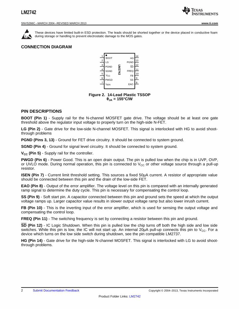
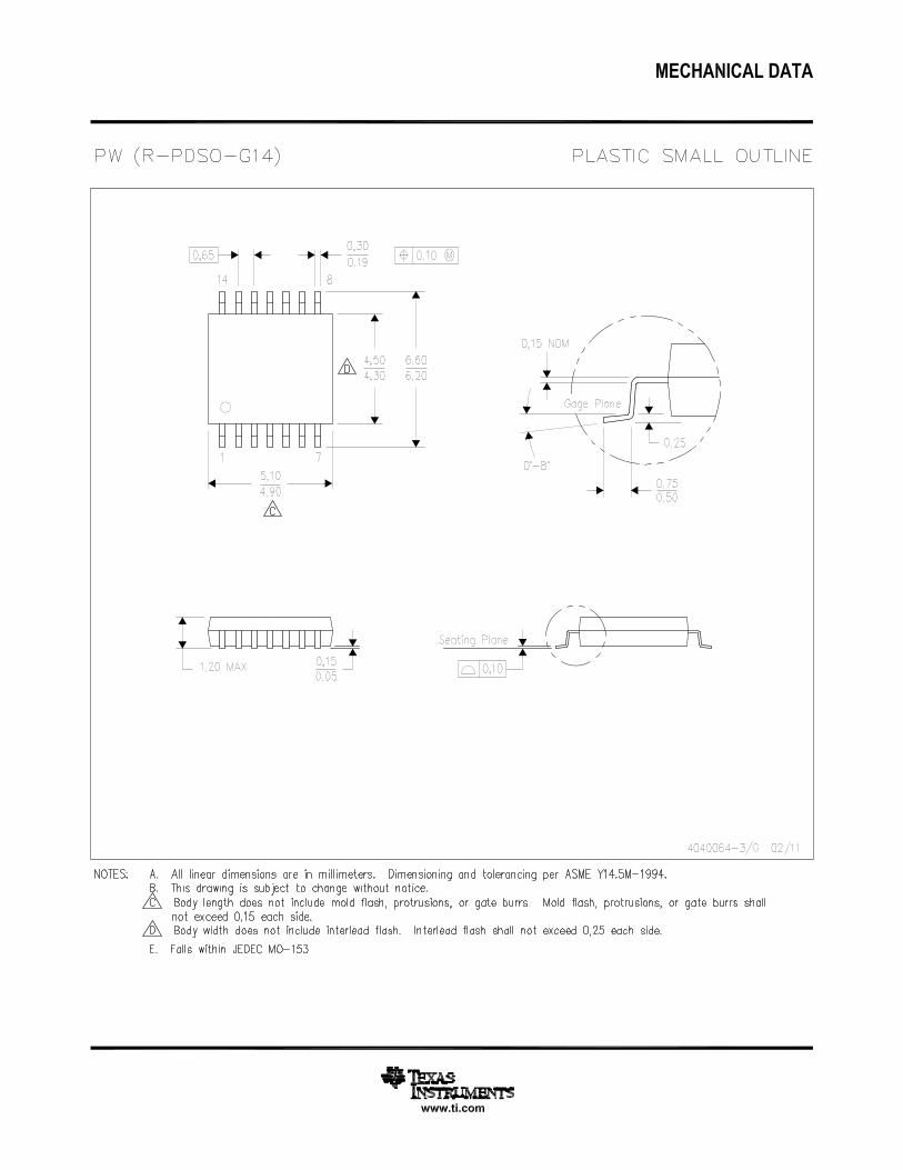
CONNECTION DIAGRAM
Figure 2. 14-Lead Plastic TSSOPθJA = 155°C/W
PIN DESCRIPTIONS
BOOT (Pin 1) - Supply rail for the N-channel MOSFET gate drive. The voltage should be at least one gatethreshold above the regulator input voltage to properly turn on the high-side N-FET.
LG (Pin 2) - Gate drive for the low-side N-channel MOSFET. This signal is interlocked with HG to avoid shoot-through problems
PGND (Pins 3, 13) - Ground for FET drive circuitry. It should be connected to system ground.
SGND (Pin 4) - Ground for signal level circuitry. It should be connected to system ground.
VCC (Pin 5) - Supply rail for the controller.
PWGD (Pin 6) - Power Good. This is an open drain output. The pin is pulled low when the chip is in UVP, OVP,or UVLO mode. During normal operation, this pin is connected to VCC or other voltage source through a pull-upresistor.
ISEN (Pin 7) - Current limit threshold setting. This sources a fixed 50µA current. A resistor of appropriate valueshould be connected between this pin and the drain of the low-side FET.
EAO (Pin 8) - Output of the error amplifier. The voltage level on this pin is compared with an internally generatedramp signal to determine the duty cycle. This pin is necessary for compensating the control loop.
SS (Pin 9) - Soft start pin. A capacitor connected between this pin and ground sets the speed at which the outputvoltage ramps up. Larger capacitor value results in slower output voltage ramp but also lower inrush current.
FB (Pin 10) - This is the inverting input of the error amplifier, which is used for sensing the output voltage andcompensating the control loop.
FREQ (Pin 11) - The switching frequency is set by connecting a resistor between this pin and ground.
SD (Pin 12) - IC Logic Shutdown. When this pin is pulled low the chip turns off both the high side and low sideswitches. While this pin is low, the IC will not start up. An internal 20µA pull-up connects this pin to VCC. For adevice which turns on the low side switch during shutdown, see the pin compatible LM2737.
HG (Pin 14) - Gate drive for the high-side N-channel MOSFET. This signal is interlocked with LG to avoid shoot-through problems.
2 Submit Documentation Feedback Copyright © 2004–2013, Texas Instruments Incorporated
Product Folder Links: LM2742
LM2742
www.ti.com SNVS266C –MARCH 2004–REVISED MARCH 2013
ABSOLUTE MAXIMUM RATINGS (1)
If Military/Aerospace specified devices are required, contact the Texas Instruments Semiconductor Sales Office/Distributors for availability and specifications.VCC 7V
BOOTV 21V
LG and HG to GND (2) -2V to 21V
Junction Temperature 150°C
Storage Temperature −65°C to 150°C
Soldering Information Lead
Temperature (soldering, 10sec) 260°C
Infrared or Convection (20sec) 235°C
ESD Rating 2 kV
(1) Absolute maximum ratings indicate limits beyond which damage to the device may occur. Operating ratings indicate conditions forwhich the device operates correctly. Operating Ratings do not imply ensured performance limits.
(2) The LG and HG pin can have -2V to -0.5V applied for a maximum duty cycle of 10% with a maximum period of 1 second. There is noduty cycle or maximum period limitation for a LG and HG pin voltage range of -0.5V to 21V.
RECOMMENDED OPERATING CONDITIONSSupply Voltage (VCC) 4.5V to 5.5V
Junction Temperature Range −40°C to +125°C
Thermal Resistance (θJA) 155°C/W
Copyright © 2004–2013, Texas Instruments Incorporated Submit Documentation Feedback 3
Product Folder Links: LM2742
LM2742
SNVS266C –MARCH 2004–REVISED MARCH 2013 www.ti.com
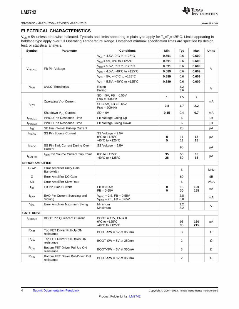
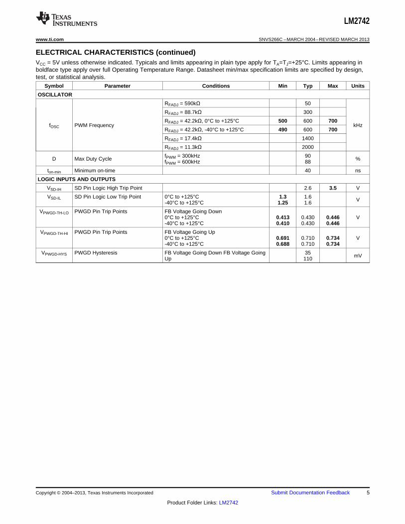
ELECTRICAL CHARACTERISTICSVCC = 5V unless otherwise indicated. Typicals and limits appearing in plain type apply for TA=TJ=+25°C. Limits appearing inboldface type apply over full Operating Temperature Range. Datasheet min/max specification limits are specified by design,test, or statistical analysis.
Symbol Parameter Conditions Min Typ Max Units
VCC = 4.5V, 0°C to +125°C 0.591 0.6 0.609
VCC = 5V, 0°C to +125°C 0.591 0.6 0.609
VCC = 5.5V, 0°C to +125°C 0.591 0.6 0.609VFB_ADJ FB Pin Voltage V
VCC = 4.5V, −40°C to +125°C 0.589 0.6 0.609
VCC = 5V, −40°C to +125°C 0.589 0.6 0.609
VCC = 5.5V, −40°C to +125°C 0.589 0.6 0.609
VON UVLO Thresholds Rising 4.2 VFalling 3.6
SD = 5V, FB = 0.55V 1 1.5 2Fsw = 600kHzOperating VCC Current mA
IQ-V5 SD = 5V, FB = 0.65V 0.8 1.7 2.2Fsw = 600kHz
Shutdown VCC Current SD = 0V 0.15 0.4 0.7 mA
tPWGD1 PWGD Pin Response Time FB Voltage Going Up 6 µs
tPWGD2 PWGD Pin Response Time FB Voltage Going Down 6 µs
ISD SD Pin Internal Pull-up Current 20 µA
ISS-ON SS Pin Source Current SS Voltage = 2.5V0°C to +125°C 8 11 15 µA-40°C to +125°C 5 11 15
ISS-OC SS Pin Sink Current During Over SS Voltage = 2.5V 95 µACurrent
ISEN Pin Source Current Trip Point 0°C to +125°C 35 50 65ISEN-TH µA-40°C to +125°C 28 50 65
ERROR AMPLIFIER
GBW Error Amplifier Unity Gain 5 MHzBandwidth
G Error Amplifier DC Gain 60 dB
SR Error Amplifier Slew Rate 6 V/µA
IFB FB Pin Bias Current FB = 0.55V 0 15 100 nAFB = 0.65V 0 30 155
IEAO EAO Pin Current Sourcing and VEAO = 2.5, FB = 0.55V 2.8 mASinking VEAO = 2.5, FB = 0.65V 0.8
VEA Error Amplifier Maximum Swing Minimum 1.2 VMaximum 3.2
GATE DRIVE
IQ-BOOT BOOT Pin Quiescent Current BOOT = 12V, EN = 00°C to +125°C 95 160 µA-40°C to +125°C 95 215
RDS1 Top FET Driver Pull-Up ON BOOT-SW = 5V at 350mA 3 Ωresistance
RDS2 Top FET Driver Pull-Down ON BOOT-SW = 5V at 350mA 2 Ωresistance
RDS3 Bottom FET Driver Pull-Up ON BOOT-SW = 5V at 350mA 3 Ωresistance
RDS4 Bottom FET Driver Pull-Down ON BOOT-SW = 5V at 350mA 2 Ωresistance
4 Submit Documentation Feedback Copyright © 2004–2013, Texas Instruments Incorporated
Product Folder Links: LM2742
LM2742
www.ti.com SNVS266C –MARCH 2004–REVISED MARCH 2013
ELECTRICAL CHARACTERISTICS (continued)VCC = 5V unless otherwise indicated. Typicals and limits appearing in plain type apply for TA=TJ=+25°C. Limits appearing inboldface type apply over full Operating Temperature Range. Datasheet min/max specification limits are specified by design,test, or statistical analysis.
Symbol Parameter Conditions Min Typ Max Units
OSCILLATOR
RFADJ = 590kΩ 50
RFADJ = 88.7kΩ 300
RFADJ = 42.2kΩ, 0°C to +125°C 500 600 700fOSC PWM Frequency kHz
RFADJ = 42.2kΩ, -40°C to +125°C 490 600 700
RFADJ = 17.4kΩ 1400
RFADJ = 11.3kΩ 2000
fPWM = 300kHz 90D Max Duty Cycle %fPWM = 600kHz 88
ton-min Minimum on-time 40 ns
LOGIC INPUTS AND OUTPUTS
VSD-IH SD Pin Logic High Trip Point 2.6 3.5 V
VSD-IL SD Pin Logic Low Trip Point 0°C to +125°C 1.3 1.6 V-40°C to +125°C 1.25 1.6
VPWGD-TH-LO PWGD Pin Trip Points FB Voltage Going Down0°C to +125°C 0.413 0.430 0.446 V-40°C to +125°C 0.410 0.430 0.446
VPWGD-TH-HI PWGD Pin Trip Points FB Voltage Going Up0°C to +125°C 0.691 0.710 0.734 V-40°C to +125°C 0.688 0.710 0.734
VPWGD-HYS PWGD Hysteresis FB Voltage Going Down FB Voltage Going 35 mVUp 110
Copyright © 2004–2013, Texas Instruments Incorporated Submit Documentation Feedback 5
Product Folder Links: LM2742
PW
M F
RE
QU
EN
CY
(kH
z)
612
614
616
618
620
622
624
626
628
630
AMBIENT TEMPERATURE (oC)
0 10 20 25 35 45 55 65 75 85 95105115 125
7
7.2
7.4
7.6
7.8
8
8.2
8.4
8.6
BO
OT
PIN
CU
RR
EN
T (
mA
)
AMBIENT TEMPERATURE (oC)
0 10 20 25 35 45 55 65 75 85 95 105115125
AMBIENT TEMPERATURE (oC)
OP
EA
RT
ING
CU
RR
EN
T(m
A)
0 20 35 55 75 95 115
Without Bootstrap
(Vboot = 12V)
With Bootstrap
(Vboot = 5V)
1.46
1.48
1.5
1.52
1.54
1.56
1.58
1.6
1.62
1.64
BO
OT
PIN
CU
RR
EN
T (
mA
)
28.9
29.1
29.3
29.5
29.7
29.9
30.1
30.3
AMBIENT TEMPERATURE (oC)
0 10 20 25 35 45 55 65 75 85 95105115125
20
30
40
50
60
70
80
90
100
0.2 1 3 5 7 9
OUTPUT CURRENT (A)
EF
FIC
IEN
CY
(%
)
Vin = 5V
Vin = 12V
Vin = 3.3V
30
40
50
60
70
80
90
100
0.1 0.5 2 4 6 8 10
Vin = 5V
Vin = 12V
OUTPUT CURRENT (A)
EF
FIC
IEN
CY
(%
)
LM2742
SNVS266C –MARCH 2004–REVISED MARCH 2013 www.ti.com
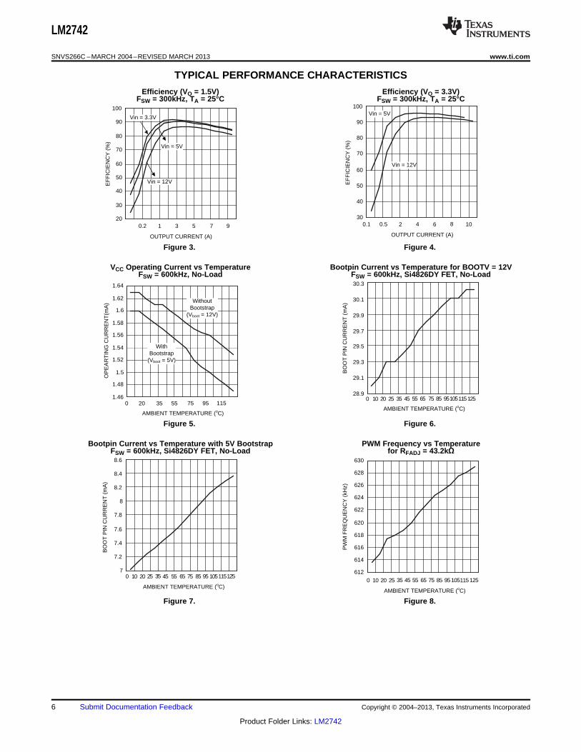
TYPICAL PERFORMANCE CHARACTERISTICS
Efficiency (VO = 1.5V) Efficiency (VO = 3.3V)FSW = 300kHz, TA = 25°C FSW = 300kHz, TA = 25°C
Figure 3. Figure 4.
VCC Operating Current vs Temperature Bootpin Current vs Temperature for BOOTV = 12VFSW = 600kHz, No-Load FSW = 600kHz, Si4826DY FET, No-Load
Figure 5. Figure 6.
Bootpin Current vs Temperature with 5V Bootstrap PWM Frequency vs TemperatureFSW = 600kHz, Si4826DY FET, No-Load for RFADJ = 43.2kΩ
Figure 7. Figure 8.
6 Submit Documentation Feedback Copyright © 2004–2013, Texas Instruments Incorporated
Product Folder Links: LM2742
VC
C P
LUS
BO
OT
CU
RR
EN
T
0
5
10
15
20
25
30
35
40
100300 500 700 9001100 1300150017001900
PWM FREQUENCY (kHz)
10
15
20
25
30
9001000110012001300140015001600170018001900
PWM FREQUENCY (kHz)
RF
-AD
J (k:
)
PWM FREQUENCY (kHz)
RF
-AD
J (k:
)
0
100
200
300
400
500
100 150 200250 300 350 400450 500 600 700 800
LM2742
www.ti.com SNVS266C –MARCH 2004–REVISED MARCH 2013
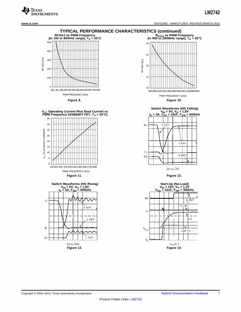
TYPICAL PERFORMANCE CHARACTERISTICS (continued)RFADJ vs PWM Frequency RFADJ vs PWM Frequency
(in 100 to 800kHz range), TA = 25°C (in 900 to 2000kHz range), TA = 25°C
Figure 9. Figure 10.
Switch Waveforms (HG Falling)VCC Operating Current Plus Boot Current vs VIN = 5V, VO = 1.8VPWM Frequency (Si4826DY FET, TA = 25°C) IO = 3A, CSS = 10nF, FSW = 600kHz
Figure 11. Figure 12.
Switch Waveforms (HG Rising) Start-Up (No-Load)VIN = 5V, VO = 1.8V VIN = 10V, VO = 1.2V
IO = 3A, FSW = 600kHz CSS = 10nF, FSW = 300kHz
Figure 13. Figure 14.
Copyright © 2004–2013, Texas Instruments Incorporated Submit Documentation Feedback 7
Product Folder Links: LM2742
400 Ps/DIV
2.0V
500 mA/div
5.0V
IIN
VSD
VCSS
VO Pre-bias = 1.2V
40 Ps/DIV
500 mV
2.0V
1A/div
5.0V
IIN
VSD
VCSS
VO
20 Ps/DIV
IIN
VSD
VCSS
VO
2.0V
2A/div
5.0V
Pre-bias = 1.2V
VO = 2.5
LM2742
SNVS266C –MARCH 2004–REVISED MARCH 2013 www.ti.com
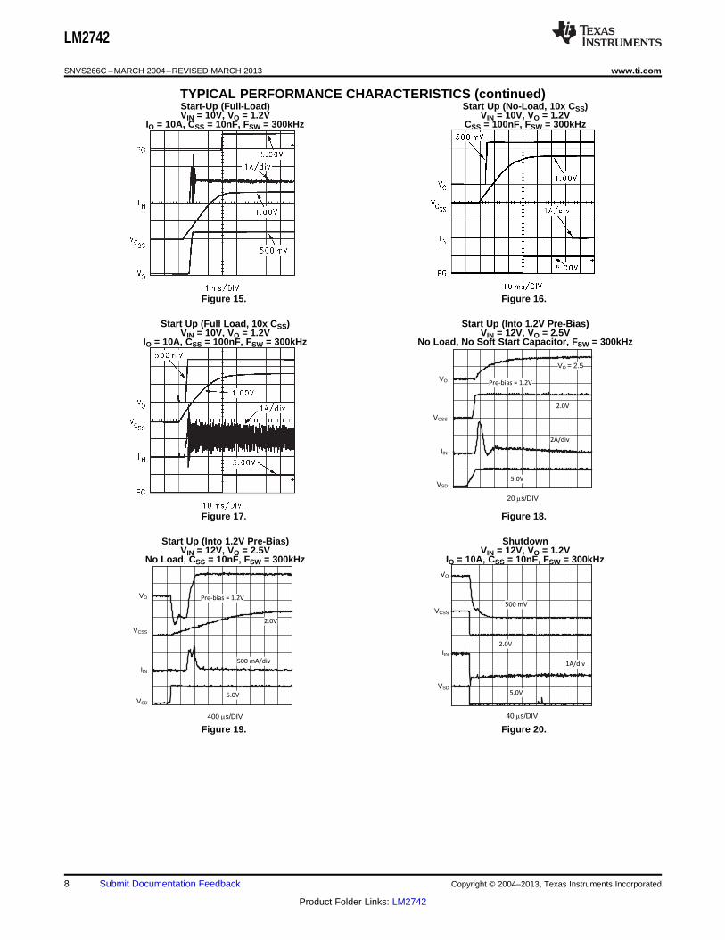
TYPICAL PERFORMANCE CHARACTERISTICS (continued)Start-Up (Full-Load) Start Up (No-Load, 10x CSS)VIN = 10V, VO = 1.2V VIN = 10V, VO = 1.2V
IO = 10A, CSS = 10nF, FSW = 300kHz CSS = 100nF, FSW = 300kHz
Figure 15. Figure 16.
Start Up (Full Load, 10x CSS) Start Up (Into 1.2V Pre-Bias)VIN = 10V, VO = 1.2V VIN = 12V, VO = 2.5V
IO = 10A, CSS = 100nF, FSW = 300kHz No Load, No Soft Start Capacitor, FSW = 300kHz
Figure 17. Figure 18.
Start Up (Into 1.2V Pre-Bias) ShutdownVIN = 12V, VO = 2.5V VIN = 12V, VO = 1.2V
No Load, CSS = 10nF, FSW = 300kHz IO = 10A, CSS = 10nF, FSW = 300kHz
Figure 19. Figure 20.
8 Submit Documentation Feedback Copyright © 2004–2013, Texas Instruments Incorporated
Product Folder Links: LM2742
40 Ps/DIV
500 mV
2.0V
1A/div
5.0V
IIN
VSD
VCSS
VO
LM2742
www.ti.com SNVS266C –MARCH 2004–REVISED MARCH 2013
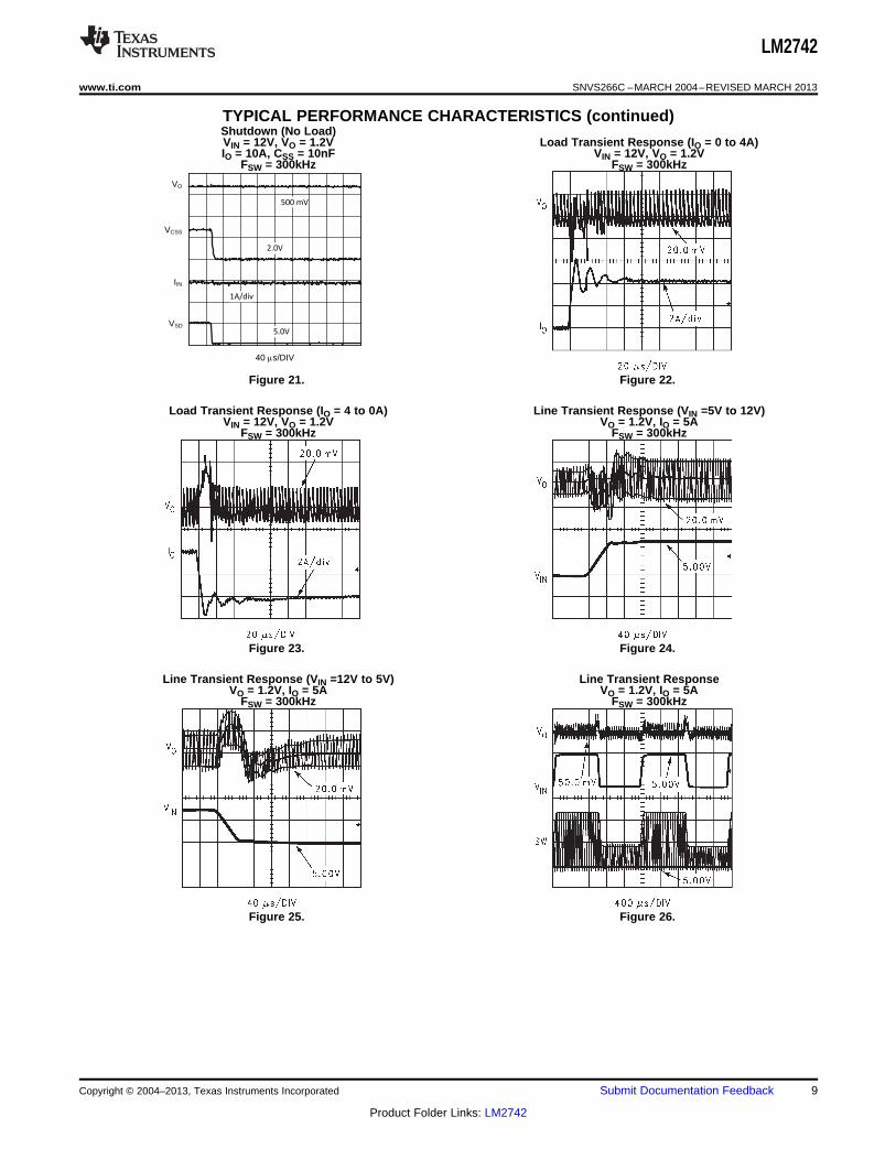
TYPICAL PERFORMANCE CHARACTERISTICS (continued)Shutdown (No Load)VIN = 12V, VO = 1.2V Load Transient Response (IO = 0 to 4A)IO = 10A, CSS = 10nF VIN = 12V, VO = 1.2V
FSW = 300kHz FSW = 300kHz
Figure 21. Figure 22.
Load Transient Response (IO = 4 to 0A) Line Transient Response (VIN =5V to 12V)VIN = 12V, VO = 1.2V VO = 1.2V, IO = 5A
FSW = 300kHz FSW = 300kHz
Figure 23. Figure 24.
Line Transient Response (VIN =12V to 5V) Line Transient ResponseVO = 1.2V, IO = 5A VO = 1.2V, IO = 5A
FSW = 300kHz FSW = 300kHz
Figure 25. Figure 26.
Copyright © 2004–2013, Texas Instruments Incorporated Submit Documentation Feedback 9
Product Folder Links: LM2742
200 Ps/DIV
VO
IL
VSW
VCSS
2A/DIV
2V/DIV
2V/DIV
10V/DIV
4 Ps/DIV
VO
IL
VSW
VCSS
2A/DIV
2V/DIV
2V/DIV
10V/DIV
LM2742
SNVS266C –MARCH 2004–REVISED MARCH 2013 www.ti.com
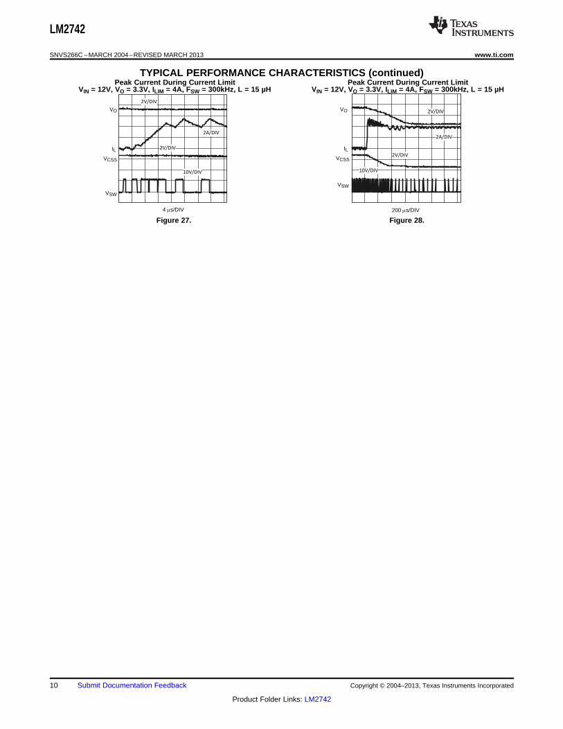
TYPICAL PERFORMANCE CHARACTERISTICS (continued)Peak Current During Current Limit Peak Current During Current Limit
VIN = 12V, VO = 3.3V, ILIM = 4A, FSW = 300kHz, L = 15 µH VIN = 12V, VO = 3.3V, ILIM = 4A, FSW = 300kHz, L = 15 µH
Figure 27. Figure 28.
10 Submit Documentation Feedback Copyright © 2004–2013, Texas Instruments Incorporated
Product Folder Links: LM2742
BG =
0.6V
50 PA
10 PA
OUTPUT CLAMP
HI: 3.25V
LO: 1.25V
3.25V
1.25V
SYNCHRONOUS
DRIVER LOGIC
10 PsDELAY
0.708V
tol.=+/-2%0.42V
tol.=+/-2%
hyst.=12%
CLOCK &
RAMPLOGIC
S
R
R>
S
off
oc
UVLO
SD FREQ PGND SGND
FB EAO
BOOT
HG
LG
ISEN
PWGD
SS
PGND
95 PA
oc
off
20 PA
EA
HIGH LOW
PWM
ILIM
3.05V
SS
CMP
VCC
LM2742
www.ti.com SNVS266C –MARCH 2004–REVISED MARCH 2013
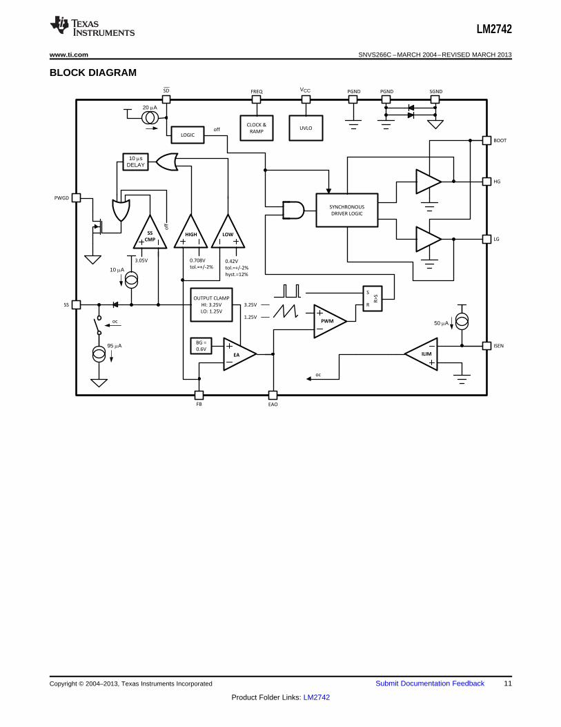
BLOCK DIAGRAM
Copyright © 2004–2013, Texas Instruments Incorporated Submit Documentation Feedback 11
Product Folder Links: LM2742
1.0526
FADJ20500
R kfreq kHz
§ · :¨ ¸¨ ¸ª º¬ ¼© ¹
ssss 5
tC
2.5 10
u
LM2742
SNVS266C –MARCH 2004–REVISED MARCH 2013 www.ti.com
APPLICATION INFORMATION
THEORY OF OPERATION
The LM2742 is a voltage-mode, high-speed synchronous buck regulator with a PWM control scheme. It isdesigned for use in set-top boxes, thin clients, DSL/Cable modems, and other applications that require highefficiency buck converters. It has power good (PWRGD), and output shutdown (SD). Current limit is achieved bysensing the voltage VDS across the low side FET. During current limit the high side gate is turned off and the lowside gate turned on. The soft start capacitor is discharged by a 95µA source (reducing the maximum duty cycle)until the current is under control.
START UP
When VCC exceeds 4.2V and the shutdown pin SD sees a logic high the soft start capacitor begins chargingthrough an internal fixed 10µA source. During this time the output of the error amplifier is allowed to rise with thevoltage of the soft start capacitor. This capacitor, CSS, determines soft start time, and can be determinedapproximately by:
(1)
An application for a microprocessor might need a delay of 3ms, in which case CSS would be 12nF. For a differentdevice, a 100ms delay might be more appropriate, in which case CSS would be 400nF. (390 10%) During softstart the PWRGD flag is forced low and is released when the voltage reaches a set value. At this point this chipenters normal operation mode and the Power Good flag is released.
Since the output is floating when the LM2742 is turned off, it is possible that the output capacitor may beprecharged to some positive value. During start-up, the LM2742 operates fully synchronous and will dischargethe output capacitor to some extent depending on the output voltage, soft start capacitance, and the size of theoutput capacitor.
NORMAL OPERATION
While in normal operation mode, the LM2742 regulates the output voltage by controlling the duty cycle of thehigh side and low side FETs. The equation governing output voltage is:
VO = 0.6 x (RFB1 + RFB2) / RFB1 (2)
The PWM frequency is adjustable between 50kHz and 2MHz and is set by an external resistor, RFADJ, betweenthe FREQ pin and ground. The resistance needed for a desired frequency is approximately:
(3)
MOSFET GATE DRIVERS
The LM2742 has two gate drivers designed for driving N-channel MOSFETs in a synchronous mode. Power forthe drivers is supplied through the BOOT pin. For the high side gate (HG) to fully turn on the top FET, the BOOTvoltage must be at least one VGS(th) greater than Vin. (BOOT ≥ 2*Vin) This voltage can be supplied by aseparate, higher voltage source, or supplied from a local charge pump structure. In a system such as a desktopcomputer, both 5V and 12V are usually available. Hence if Vin was 5V, the 12V supply could be used for BOOT.12V is more than 2*Vin, so the HG would operate correctly. For a BOOT of 12V, the initial gate charging currentis 2A, and the initial gate discharging current is typically 6A.
12 Submit Documentation Feedback Copyright © 2004–2013, Texas Instruments Incorporated
Product Folder Links: LM2742
+
+
LG
HG
BOOT
LM2742
D1
CBOOTVCC
5V
LM2742
www.ti.com SNVS266C –MARCH 2004–REVISED MARCH 2013
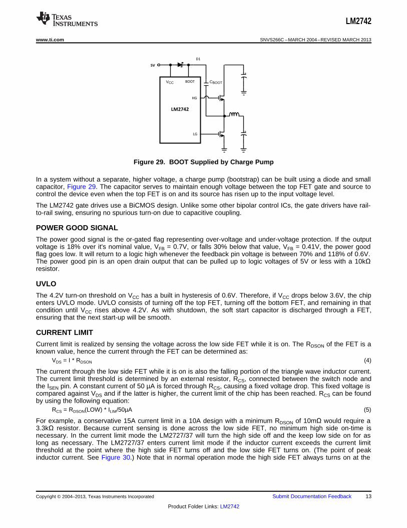
Figure 29. BOOT Supplied by Charge Pump
In a system without a separate, higher voltage, a charge pump (bootstrap) can be built using a diode and smallcapacitor, Figure 29. The capacitor serves to maintain enough voltage between the top FET gate and source tocontrol the device even when the top FET is on and its source has risen up to the input voltage level.
The LM2742 gate drives use a BiCMOS design. Unlike some other bipolar control ICs, the gate drivers have rail-to-rail swing, ensuring no spurious turn-on due to capacitive coupling.
POWER GOOD SIGNAL
The power good signal is the or-gated flag representing over-voltage and under-voltage protection. If the outputvoltage is 18% over it's nominal value, VFB = 0.7V, or falls 30% below that value, VFB = 0.41V, the power goodflag goes low. It will return to a logic high whenever the feedback pin voltage is between 70% and 118% of 0.6V.The power good pin is an open drain output that can be pulled up to logic voltages of 5V or less with a 10kΩresistor.
UVLO
The 4.2V turn-on threshold on VCC has a built in hysteresis of 0.6V. Therefore, if VCC drops below 3.6V, the chipenters UVLO mode. UVLO consists of turning off the top FET, turning off the bottom FET, and remaining in thatcondition until VCC rises above 4.2V. As with shutdown, the soft start capacitor is discharged through a FET,ensuring that the next start-up will be smooth.
CURRENT LIMIT
Current limit is realized by sensing the voltage across the low side FET while it is on. The RDSON of the FET is aknown value, hence the current through the FET can be determined as:
VDS = I * RDSON (4)
The current through the low side FET while it is on is also the falling portion of the triangle wave inductor current.The current limit threshold is determined by an external resistor, RCS, connected between the switch node andthe ISEN pin. A constant current of 50 µA is forced through RCS, causing a fixed voltage drop. This fixed voltage iscompared against VDS and if the latter is higher, the current limit of the chip has been reached. RCS can be foundby using the following equation:
RCS = RDSON(LOW) * ILIM/50µA (5)
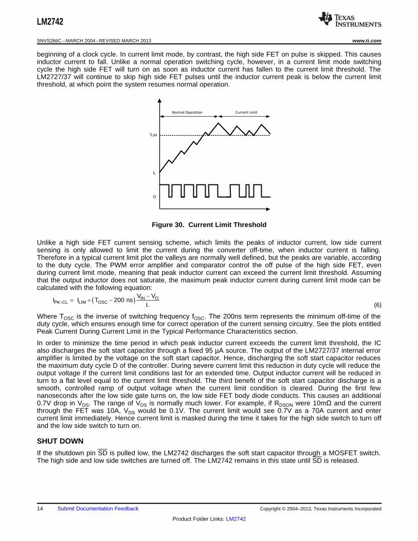
For example, a conservative 15A current limit in a 10A design with a minimum RDSON of 10mΩ would require a3.3kΩ resistor. Because current sensing is done across the low side FET, no minimum high side on-time isnecessary. In the current limit mode the LM2727/37 will turn the high side off and the keep low side on for aslong as necessary. The LM2727/37 enters current limit mode if the inductor current exceeds the current limitthreshold at the point where the high side FET turns off and the low side FET turns on. (The point of peakinductor current. See Figure 30.) Note that in normal operation mode the high side FET always turns on at the
Copyright © 2004–2013, Texas Instruments Incorporated Submit Documentation Feedback 13
Product Folder Links: LM2742
IN OPK-CL LIM OSC
V VI I T 200 ns
L
ILIM
IL
D
Normal Operation Current Limit
LM2742
SNVS266C –MARCH 2004–REVISED MARCH 2013 www.ti.com
beginning of a clock cycle. In current limit mode, by contrast, the high side FET on pulse is skipped. This causesinductor current to fall. Unlike a normal operation switching cycle, however, in a current limit mode switchingcycle the high side FET will turn on as soon as inductor current has fallen to the current limit threshold. TheLM2727/37 will continue to skip high side FET pulses until the inductor current peak is below the current limitthreshold, at which point the system resumes normal operation.
Figure 30. Current Limit Threshold
Unlike a high side FET current sensing scheme, which limits the peaks of inductor current, low side currentsensing is only allowed to limit the current during the converter off-time, when inductor current is falling.Therefore in a typical current limit plot the valleys are normally well defined, but the peaks are variable, accordingto the duty cycle. The PWM error amplifier and comparator control the off pulse of the high side FET, evenduring current limit mode, meaning that peak inductor current can exceed the current limit threshold. Assumingthat the output inductor does not saturate, the maximum peak inductor current during current limit mode can becalculated with the following equation:
(6)
Where TOSC is the inverse of switching frequency fOSC. The 200ns term represents the minimum off-time of theduty cycle, which ensures enough time for correct operation of the current sensing circuitry. See the plots entitledPeak Current During Current Limit in the Typical Performance Characteristics section.
In order to minimize the time period in which peak inductor current exceeds the current limit threshold, the ICalso discharges the soft start capacitor through a fixed 95 µA source. The output of the LM2727/37 internal erroramplifier is limited by the voltage on the soft start capacitor. Hence, discharging the soft start capacitor reducesthe maximum duty cycle D of the controller. During severe current limit this reduction in duty cycle will reduce theoutput voltage if the current limit conditions last for an extended time. Output inductor current will be reduced inturn to a flat level equal to the current limit threshold. The third benefit of the soft start capacitor discharge is asmooth, controlled ramp of output voltage when the current limit condition is cleared. During the first fewnanoseconds after the low side gate turns on, the low side FET body diode conducts. This causes an additional0.7V drop in VDS. The range of VDS is normally much lower. For example, if RDSON were 10mΩ and the currentthrough the FET was 10A, VDS would be 0.1V. The current limit would see 0.7V as a 70A current and entercurrent limit immediately. Hence current limit is masked during the time it takes for the high side switch to turn offand the low side switch to turn on.
SHUT DOWN
If the shutdown pin SD is pulled low, the LM2742 discharges the soft start capacitor through a MOSFET switch.The high side and low side switches are turned off. The LM2742 remains in this state until SD is released.
14 Submit Documentation Feedback Copyright © 2004–2013, Texas Instruments Incorporated
Product Folder Links: LM2742
OIN DC
I DI
K
in
max
VL
didt
' § ·¨ ¸© ¹
2rms rip
D 2
I ESRP
n
LM2742
www.ti.com SNVS266C –MARCH 2004–REVISED MARCH 2013
DESIGN CONSIDERATIONS
The following is a design procedure for all the components needed to create the circuit shown in Figure 32 in theExample Circuits section, a 5V in to 1.2V out converter, capable of delivering 10A with an efficiency of 85%. Theswitching frequency is 300kHz. The same procedures can be followed to create many other designs with varyinginput voltages, output voltages, and output currents.
Input Capacitor
The input capacitors in a Buck switching converter are subjected to high stress due to the input currentwaveform, which is a square wave. Hence input caps are selected for their ripple current capability and theirability to withstand the heat generated as that ripple current runs through their ESR. Input rms ripple current isapproximately:
png (7)
The power dissipated by each input capacitor is:
(8)
Here, n is the number of capacitors, and indicates that power loss in each cap decreases rapidly as the numberof input caps increase. The worst-case ripple for a Buck converter occurs during full load, when the duty cycle D= 50%.
In the 5V to 1.2V case, D = 1.2/5 = 0.24. With a 10A maximum load the ripple current is 4.3A. The Sanyo10MV5600AX aluminum electrolytic capacitor has a ripple current rating of 2.35A, up to 105°C. Two suchcapacitors make a conservative design that allows for unequal current sharing between individual caps. Eachcapacitor has a maximum ESR of 18mΩ at 100 kHz. Power loss in each device is then 0.05W, and total loss is0.1W. Other possibilities for input and output capacitors include MLCC, tantalum, OSCON, SP, and POSCAPS.
Input Inductor
The input inductor serves two basic purposes. First, in high power applications, the input inductor helps insulatethe input power supply from switching noise. This is especially important if other switching converters drawcurrent from the same supply. Noise at high frequency, such as that developed by the LM2742 at 1MHzoperation, could pass through the input stage of a slower converter, contaminating and possibly interfering withits operation.
An input inductor also helps shield the LM2742 from high frequency noise generated by other switchingconverters. The second purpose of the input inductor is to limit the input current slew rate. During a change fromno-load to full-load, the input inductor sees the highest voltage change across it, equal to the full load currenttimes the input capacitor ESR. This value divided by the maximum allowable input current slew rate gives theminimum input inductance:
(9)
In the case of a desktop computer system, the input current slew rate is the system power supply or "silver box"output current slew rate, which is typically about 0.1A/µs. Total input capacitor ESR is 9mΩ, hence ΔV is10*0.009 = 90 mV, and the minimum inductance required is 0.9µH. The input inductor should be rated to handlethe DC input current, which is approximated by:
(10)
In this case IIN-DC is about 2.8A. One possible choice is the TDK SLF12575T-1R2N8R2, a 1.2µH device that canhandle 8.2Arms, and has a DCR of 7mΩ.
Copyright © 2004–2013, Texas Instruments Incorporated Submit Documentation Feedback 15
Product Folder Links: LM2742
oMAX
o
VESR
I
'
'
LM2742
SNVS266C –MARCH 2004–REVISED MARCH 2013 www.ti.com
Output Inductor
The output inductor forms the first half of the power stage in a Buck converter. It is responsible for smoothing thesquare wave created by the switching action and for controlling the output current ripple. (ΔIo) The inductance ischosen by selecting between tradeoffs in output ripple, efficiency, and response time. The smaller the outputinductor, the more quickly the converter can respond to transients in the load current. If the inductor value isincreased, the ripple through the output capacitor is reduced and thus the output ripple is reduced. As shown inthe efficiency calculations, a smaller inductor requires a higher switching frequency to maintain the same level ofoutput current ripple. An increase in frequency can mean increasing loss in the FETs due to the charging anddischarging of the gates. Generally the switching frequency is chosen so that conduction loss outweighsswitching loss. The equation for output inductor selection is:
(11)
A good range for ΔIo is 25 to 50% of the output current. In the past, 30% was considered a maximum value foroutput currents higher than about 2Amps, but as output capacitor technology improves the ripple current can beallowed to increase. Plugging in the values for output current ripple, input voltage, output voltage, switchingfrequency, and assuming a 40% peak-to-peak output current ripple yields an inductance of 1.5µH. The outputinductor must be rated to handle the peak current (also equal to the peak switch current), which is (Io + 0.5*ΔIo).This is 12A for a 10A design. The Coilcraft D05022-152HC is 1.5µH, is rated to 15Arms, and has a DCR of 4mΩ.
Output Capacitor
The output capacitor forms the second half of the power stage of a Buck switching converter. It is used to controlthe output voltage ripple (ΔVo) and to supply load current during fast load transients.
In this example the output current is 10A and the expected type of capacitor is an aluminum electrolytic, as withthe input capacitors. (Other possibilities include ceramic, tantalum, and solid electrolyte capacitors, however theceramic type often do not have the large capacitance needed to supply current for load transients, and tantalumstend to be more expensive than aluminum electrolytic.) Aluminum capacitors tend to have very high capacitanceand fairly low ESR, meaning that the ESR zero, which affects system stability, will be much lower than theswitching frequency. The large capacitance means that at switching frequency, the ESR is dominant, hence thetype and number of output capacitors is selected on the basis of ESR. One simple formula to find the maximumESR based on the desired output voltage ripple, ΔVo and the designed output current ripple, ΔIo, is:
(12)
In this example, in order to maintain a 2% peak-to-peak output voltage ripple and a 40% peak-to-peak inductorcurrent ripple, the required maximum ESR is 6mΩ. Three Sanyo 10MV5600AX capacitors in parallel will give anequivalent ESR of 6mΩ. The total bulk capacitance of 16.8mF is enough to supply even severe load transients.Using the same capacitors for both input and output also keeps the bill of materials simple.
MOSFETS
MOSFETS are a critical part of any switching controller and have a direct impact on the system efficiency. In thiscase the target efficiency is 85% and this is the variable that will determine which devices are acceptable. Lossfrom the capacitors, inductors, and the LM2742 is detailed in the Efficiency section, and come to about 0.54W.To meet the target efficiency, this leaves 1.45W for the FET conduction loss, gate charging loss, and switchingloss. Switching loss is particularly difficult to estimate because it depends on many factors. When the loadcurrent is more than about 1 or 2 amps, conduction losses outweigh the switching and gate charging losses. Thisallows FET selection based on the RDSON of the FET. Adding the FET switching and gate-charging losses to theequation leaves 1.2W for conduction losses. The equation for conduction loss is:
PCnd = D(I2o * RDSON *k) + (1-D)(I2o * RDSON *k) (13)
The factor k is a constant which is added to account for the increasing RDSON of a FET due to heating. Here, k =1.3. The Si4442DY has a typical RDSON of 4.1mΩ. When plugged into the equation for PCND the result is a loss of0.533W. If this design were for a 5V to 2.5V circuit, an equal number of FETs on the high and low sides would bethe best solution. With the duty cycle D = 0.24, it becomes apparent that the low side FET carries the loadcurrent 76% of the time. Adding a second FET in parallel to the bottom FET could improve the efficiency bylowering the effective RDSON. The lower the duty cycle, the more effective a second or even third FET can be. Fora minimal increase in gate charging loss (0.054W) the decrease in conduction loss is 0.15W. What was an 85%design improves to 86% for the added cost of one SO-8 MOSFET.
16 Submit Documentation Feedback Copyright © 2004–2013, Texas Instruments Incorporated
Product Folder Links: LM2742
o
o total loss
P
P P
K
LM2742
www.ti.com SNVS266C –MARCH 2004–REVISED MARCH 2013
Control Loop Components
The circuit is this design example and the others shown in the Example Circuits section have been compensatedto improve their DC gain and bandwidth. The result of this compensation is better line and load transientresponses. For the LM2742, the top feedback divider resistor, Rfb2, is also a part of the compensation. For the10A, 5V to 1.2V design, the values are:
Cc1 = 4.7pF 10%, Cc2 = 1nF 10%, Rc = 229kΩ 1%. These values give a phase margin of 63° and a bandwidthof 29.3kHz.
Support Capacitors and Resistors
The Cinx capacitors are high frequency bypass devices, designed to filter harmonics of the switching frequencyand input noise. Two 1µF ceramic capacitors with a sufficient voltage rating (10V for the Circuit of Figure 32) willwork well in almost any case.
RIN and CIN are standard filter components designed to ensure smooth DC voltage for the chip supply.Depending on noise, RIN should be 10 to 100Ω, and CIN should be between 0.1 and 2.2 µF. CBOOT is thebootstrap capacitor, and should be 0.1µF. (In the case of a separate, higher supply to the BOOT pin, this 0.1µFcap can be used to bypass the supply.) Using a Schottky device for the bootstrap diode allows the minimum dropfor both high and low side drivers. The On Semiconductor BAT54 or MBR0520 work well.
Rp is a standard pull-up resistor for the open-drain power good signal, and should be 10kΩ. If this feature is notnecessary, it can be omitted.
RCS is the resistor used to set the current limit. Since the design calls for a peak current magnitude (Io + 0.5 *ΔIo) of 12A, a safe setting would be 15A. (This is well below the saturation current of the output inductor, which is25A.) Following the equation from the Current Limit section, use a 3.3kΩ resistor.
RFADJ is used to set the switching frequency of the chip. Following the equation in the Theory of Operationsection, the closest 1% tolerance resistor to obtain fSW = 300kHz is 88.7kΩ.
CSS depends on the users requirements. Based on the equation for CSS in the Theory of Operation section, for a3ms delay, a 12nF capacitor will suffice.
EFFICIENCY CALCULATIONS
A reasonable estimation of the efficiency of a switching controller can be obtained by adding together the loss iseach current carrying element and using the equation:
(14)
The following shows an efficiency calculation to complement the Circuit of Figure 32. Output power for this circuitis 1.2V x 10A = 12W.
Chip Operating LossPIQ = IQ-VCC *VCC (15)
2mA x 5V = 0.01W
FET Gate Charging LossPGC = n * VCC * QGS * fOSC (16)
The value n is the total number of FETs used. The Si4442DY has a typical total gate charge, QGS, of 36nC andan rds-on of 4.1mΩ. For a single FET on top and bottom: 2*5*36E-9*300,000 = 0.108W
FET Switching LossPSW = 0.5 * Vin * IO * (tr + tf)* fOSC (17)
The Si4442DY has a typical rise time tr and fall time tf of 11 and 47ns, respectively. 0.5*5*10*58E-9*300,000 =0.435W
FET Conduction LossPCn = 0.533W (18)
Input Capacitor Loss
Copyright © 2004–2013, Texas Instruments Incorporated Submit Documentation Feedback 17
Product Folder Links: LM2742
LM2742
HG
BOOT
LG
PGND
FB
SD
PWGD
FREQ
SS
SGND
EAO
PGND
+
+
+5V
VIN = 12V
Vo = 3.3V@10A
2 x 10 PF25V, 3.3A
4 x 100 PF10V, 55 m:
2.7 PH14.4A, 4.5 m:
Rfb2
Rfb1Cc1
Cc2 Rc1
RCS
CSS
RFADJ
RIN
CIN
D1 CBOOT
Q1
Q2
1 PF, 25V
1.2 PH8.2A, 6.9 m:
Rc2 Cc3
0.1P
1.8k
10
2.2P
88.7k
12n
270p
6.8p
143.3k
8.45k 470p
11k
49.9k
CIN1,2CINX
Co1-4
LIN
L1
VCC
ISEN
1287.5%
22 1.7
OIN
est ' d
I DI
K
INrms rip OI I D 1 D
2rms rip
Cin
I ESRP
n
LM2742
SNVS266C –MARCH 2004–REVISED MARCH 2013 www.ti.com
(19)
(20)
4.282*0.018/2 = 0.164W
Input Inductor LossPLin = I2in * DCRinput-L (21)
(22)
2.822*0.007 = 0.055W
Output Inductor LossPLout = I2o * DCRoutput-L (23)
102*0.004 = 0.4W
System Efficiency
(24)
Example Circuits
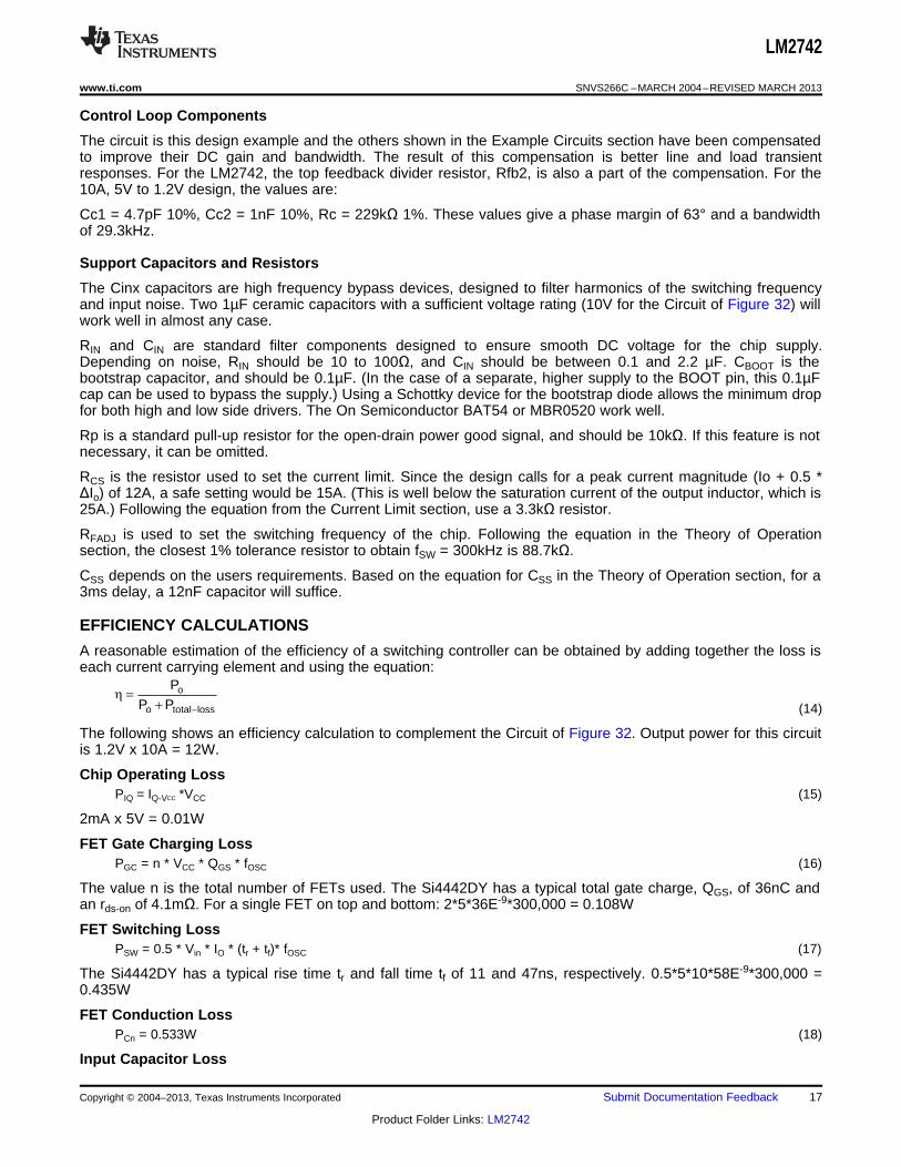
Figure 31. 5V-16V to 3.3V, 10A, 300kHz
This circuit and the one featured on the front page have been designed to deliver high current and high efficiencyin a small package, both in area and in height The tallest component in this circuit is the inductor L1, which is6mm tall. The compensation has been designed to tolerate input voltages from 5 to 16V.
18 Submit Documentation Feedback Copyright © 2004–2013, Texas Instruments Incorporated
Product Folder Links: LM2742
HG
BOOT
ISEN
LG
PGND
FB
VCC
SD
PWGD
FREQ
SS
SGND
EAO
PGND
+
+
VIN = 5V
Vo = 1.8V@3A
100 PF10V, 1.9A
1 x 220 PF4V, 55 m:
2.2 PH6.1A, 12 m:
Rfb2
Rfb1Cc1
Cc2 RC1
Rcs
Css
RFADJ
RIN
CIN
Cc
Q1/Q2
+12V
4.99k
2.49k
2.7k
12n
43.2k
10
2.2P
0.1P
10p
560p 51.1k
CIN1
Co1L1
LM2742
LM2742
HG
BOOT
ISEN
LG
PGND
FB
VCC
SD
PWGD
FREQ
SS
SGND
EAO
PGND
+
+
VIN = 5V
Vo = 1.2V@10A
3 x 5600 PF10V, 3.1A 18 m:
1.5 PH15A, 4 m:
Rfb2
Rfb1Cc1
Cc2 Rc1
RCS
CSS
RFADJ
RIN
CIN
D1 CBOOT
Q1
Q2
1.2 PH8.2A, 6.9 m:
0.1P
1.5k
10
2.2P
88.7k
12n
270p
4.7p
229k
4.99k
4.99k
Co1-3
LIN
L1
2 x 5600 PF10V, 2.35A
CIN1,22x1 PF10V
CINx1, 2
LM2742
www.ti.com SNVS266C –MARCH 2004–REVISED MARCH 2013
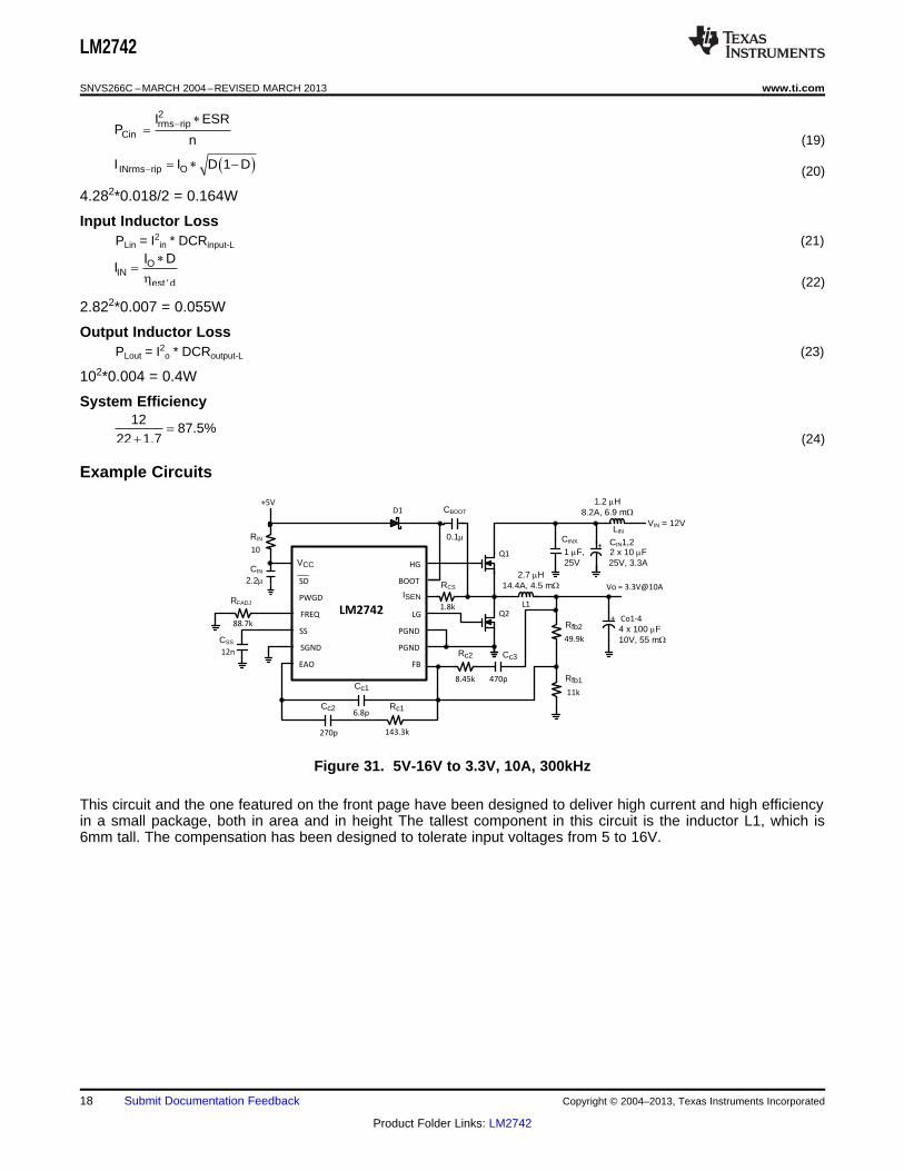
Figure 32. 5V to 1.2V, 10A, 300kHz
This circuit design, detailed in the Design Considerations section, uses inexpensive aluminum capacitors and off-the-shelf inductors. It can deliver 10A at better than 85% efficiency. Large bulk capacitance on input and outputensure stable operation.
Figure 33. 5V to 1.8V, 3A, 600kHz
The example circuit of Figure 33 has been designed for minimum component count and overall solution size. Aswitching frequency of 600kHz allows the use of small input/output capacitors and a small inductor. Theavailability of separate 5V and 12V supplies (such as those available from desk-top computer supplies) and thelow current further reduce component count. Using the 12V supply to power the MOSFET drivers eliminates thebootstrap diode, D1. At low currents, smaller FETs or dual FETs are often the most efficient solutions. Here, theSi4826DY, an asymmetric dual FET in an SO-8 package, yields 92% efficiency at a load of 2A.
Copyright © 2004–2013, Texas Instruments Incorporated Submit Documentation Feedback 19
Product Folder Links: LM2742
LM2742
HG
BOOT
ISEN
LG
PGND
FB
VCC
SD
PWGD
FREQ
SS
SGND
EAO
PGND
+
+
+5V
VIN = 5 to 15V
Vo = 1.8V@1A
1 x 15 PF25V, 3.3A
1 x 15 PF25V, 3.1 m:
3.3 PH4.1A, 17.4 m:
Rfb2
Rfb1
Rcs
Css
RFADJ
RIN
CIN
D1 CBOOT
1 PH6.4A, 7.3 m:
Rc2 Cc3
LM2742
HG
BOOT
ISEN
LG
PGND
FB
VCC
SD
PWGD
FREQ
SS
SGND
EAO
PGND
+
+
+5V
VIN = 5 to 15V
Vo = 3.3V@1A
1 x 15 PF25V, 3.3A
1 x 15 PF25V, 3.1 m:
4.7 PF3.4A, 26 m:
Rfb2
Rfb1Cc1
Rcs
D1 CBOOT
Q1/Q2
1 PF6.4A, 7.3 m:
10
2.2P
0.1P
1.5k
10k
2.21k
0.1P10
2.2P
17.4k
39n
22p
680p 10.7k
680p66.5
10k
4.99k
1.5k
17.4k
27p
1n
820p
12.1k
54.9
Co1
CIN1
LIN
L1
L1
LIN
Co1
Q1/Q2
Cc2 Rc1
Rc2 Cc3
RIN
Cc1
Cc2 Rc1
CIN
RFADJ
HG
BOOT
ISEN
LG
PGND
FB
VCC
SD
PWGD
FREQ
SS
SGND
EAO
PGND
+
+
+5V
VIN = 3.3V
Vo = 0.8V@5A
1 x 5600 PF10V, 2.35A
2 x 4700 PF16V, 2.8A
1 PH11A, 3.7 m:
Rfb2
Rfb1Cc1
Cc2 Rc1
Rcs
Css
RFADJ
RIN
CIN
D1 CBOOT
Q1
Q2
1 PF10V
1 PH4.5A, 7.5 m:
4.99k
3.3k
14.9k
147k
4.7p
680p
12n
49.9k
2.2P
100.1P
Co1,2
CIN1CINx
LIN
L1
LM2742
SNVS266C –MARCH 2004–REVISED MARCH 2013 www.ti.com
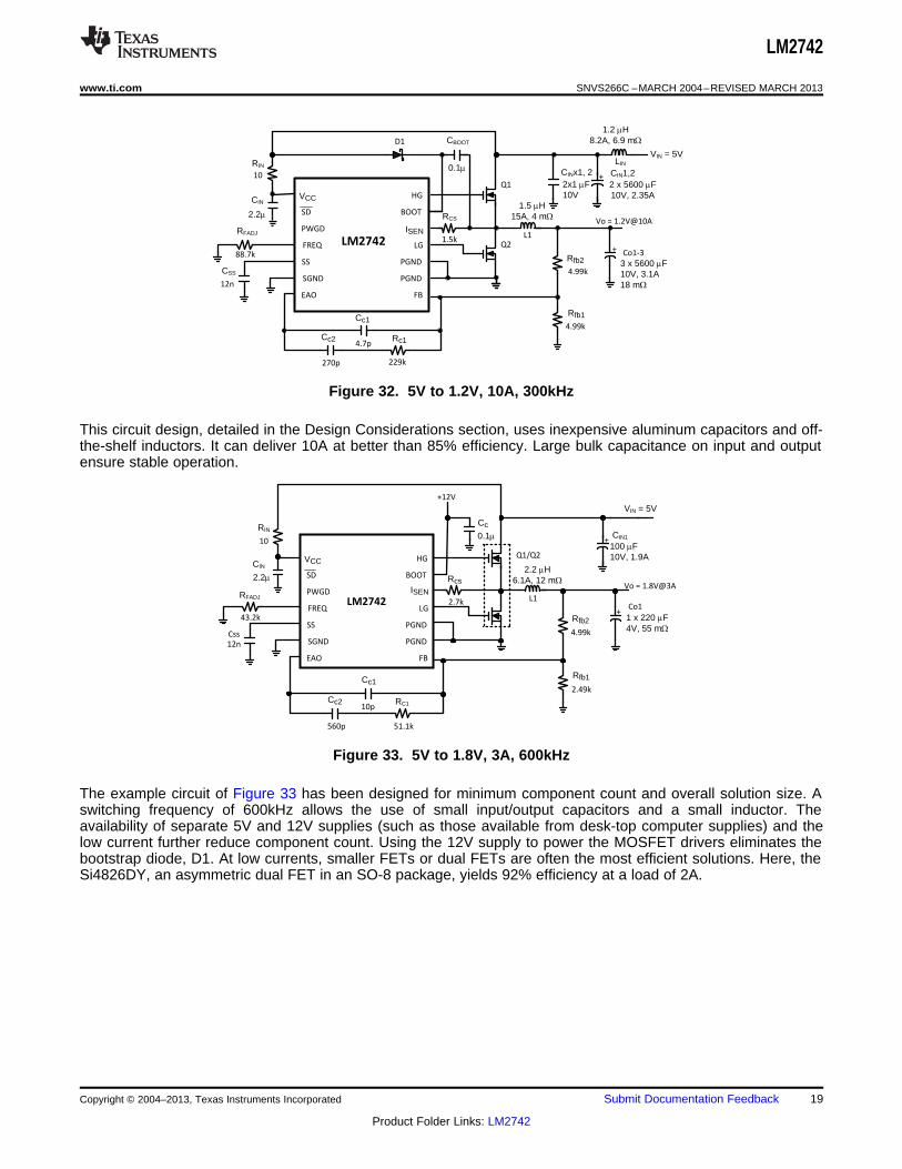
Figure 34. 3.3V to 0.8V, 5A, 500kHz
The circuit of Figure 34 demonstrates the LM2742 delivering a low output voltage at high efficiency (87%). Aseparate 5V supply is required to run the chip, however the input voltage can be as low as 2.2
Figure 35. 1.8V and 3.3V, 1A, 1.4MHz, Simultaneous
20 Submit Documentation Feedback Copyright © 2004–2013, Texas Instruments Incorporated
Product Folder Links: LM2742
LM2742
HG
BOOT
ISEN
LG
PGND
FB
VCC
SD
PWGD
FREQ
SS
SGND
EAO
PGND
+
+
VIN = 12V
Vo = [email protected]
2 x 680 PF16V26 m:
47 PH, 2.7A53 m:
RFB2
RFB1CC1
CSS
RFADJ
CIN
CBOOT
Q1
RC2 CC3
10 PF16V
10 PF6.3V
+5V (low current source)
D1
D2
10k
1.37k
22n
56p
3.9n 61.9k
750
12n
267k
0.1P
2.2P
L1
CINX
CoxCo1,2
680 PF16V1.54A
CIN1
CC2 RC1
LM2742
HG
BOOT
LG
PGND
FB
SD
PWGD
FREQ
SS
SGND
EAO
PGND
+
+
+5V
VIN = 11 to 13V
Vo = 3.3V@3A
4.2 PH, 5.5A 15 m:
CC1
RFADJ
D1
Q1/Q2
1 PH, 6.4A 7.3 m:
2 x 680 PF16V, 1.54A
LM78L05
VIN = 11 to 13VTo 2nd LM27x7
2.21k
0.1P
2k
2.2P
32.5k
12n
8.2p
1n
4.7n2.37k
52.3k
Co1,2
680 PF16V, 1.54A
10 PF16V
10k10 PF25V
Cox
ISEN
VCC
Rfb2
Rfb1
RC1
Rcs
Css
CIN
CBOOT
CIN1CINx
LIN
CC2
RC2 CC3
LM2742
www.ti.com SNVS266C –MARCH 2004–REVISED MARCH 2013
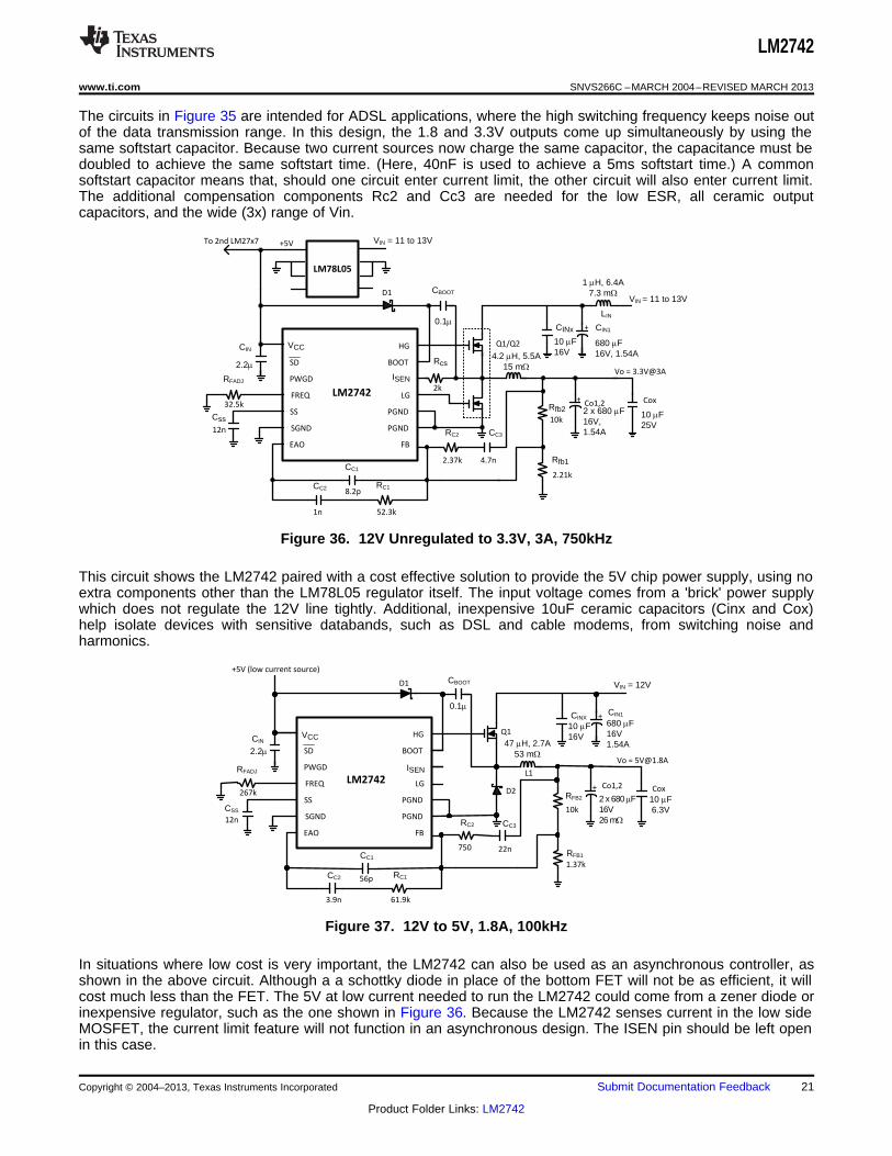
The circuits in Figure 35 are intended for ADSL applications, where the high switching frequency keeps noise outof the data transmission range. In this design, the 1.8 and 3.3V outputs come up simultaneously by using thesame softstart capacitor. Because two current sources now charge the same capacitor, the capacitance must bedoubled to achieve the same softstart time. (Here, 40nF is used to achieve a 5ms softstart time.) A commonsoftstart capacitor means that, should one circuit enter current limit, the other circuit will also enter current limit.The additional compensation components Rc2 and Cc3 are needed for the low ESR, all ceramic outputcapacitors, and the wide (3x) range of Vin.
Figure 36. 12V Unregulated to 3.3V, 3A, 750kHz
This circuit shows the LM2742 paired with a cost effective solution to provide the 5V chip power supply, using noextra components other than the LM78L05 regulator itself. The input voltage comes from a 'brick' power supplywhich does not regulate the 12V line tightly. Additional, inexpensive 10uF ceramic capacitors (Cinx and Cox)help isolate devices with sensitive databands, such as DSL and cable modems, from switching noise andharmonics.
Figure 37. 12V to 5V, 1.8A, 100kHz
In situations where low cost is very important, the LM2742 can also be used as an asynchronous controller, asshown in the above circuit. Although a a schottky diode in place of the bottom FET will not be as efficient, it willcost much less than the FET. The 5V at low current needed to run the LM2742 could come from a zener diode orinexpensive regulator, such as the one shown in Figure 36. Because the LM2742 senses current in the low sideMOSFET, the current limit feature will not function in an asynchronous design. The ISEN pin should be left openin this case.
Copyright © 2004–2013, Texas Instruments Incorporated Submit Documentation Feedback 21
Product Folder Links: LM2742
LM2742
SNVS266C –MARCH 2004–REVISED MARCH 2013 www.ti.com
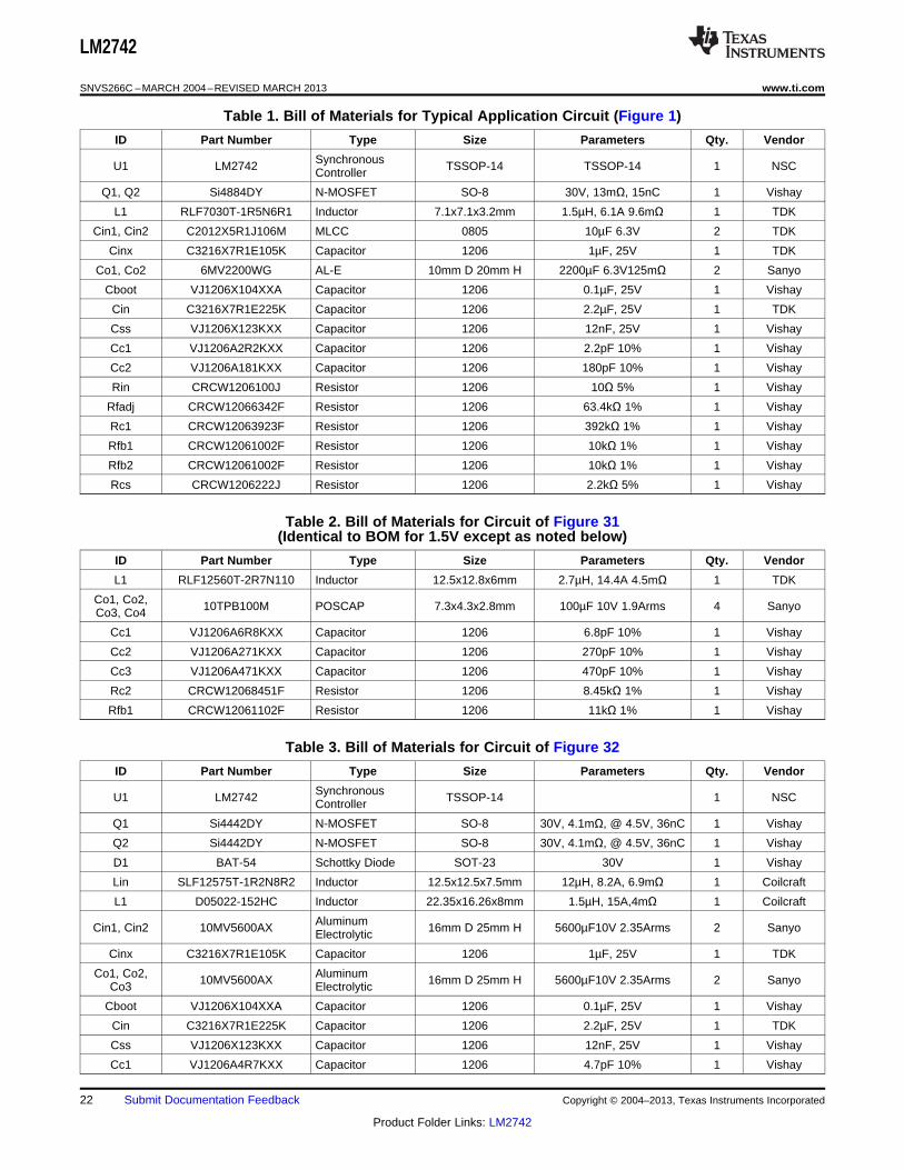
Table 1. Bill of Materials for Typical Application Circuit (Figure 1)
ID Part Number Type Size Parameters Qty. Vendor
SynchronousU1 LM2742 TSSOP-14 TSSOP-14 1 NSCController
Q1, Q2 Si4884DY N-MOSFET SO-8 30V, 13mΩ, 15nC 1 Vishay
L1 RLF7030T-1R5N6R1 Inductor 7.1x7.1x3.2mm 1.5µH, 6.1A 9.6mΩ 1 TDK
Cin1, Cin2 C2012X5R1J106M MLCC 0805 10µF 6.3V 2 TDK
Cinx C3216X7R1E105K Capacitor 1206 1µF, 25V 1 TDK
Co1, Co2 6MV2200WG AL-E 10mm D 20mm H 2200µF 6.3V125mΩ 2 Sanyo
Cboot VJ1206X104XXA Capacitor 1206 0.1µF, 25V 1 Vishay
Cin C3216X7R1E225K Capacitor 1206 2.2µF, 25V 1 TDK
Css VJ1206X123KXX Capacitor 1206 12nF, 25V 1 Vishay
Cc1 VJ1206A2R2KXX Capacitor 1206 2.2pF 10% 1 Vishay
Cc2 VJ1206A181KXX Capacitor 1206 180pF 10% 1 Vishay
Rin CRCW1206100J Resistor 1206 10Ω 5% 1 Vishay
Rfadj CRCW12066342F Resistor 1206 63.4kΩ 1% 1 Vishay
Rc1 CRCW12063923F Resistor 1206 392kΩ 1% 1 Vishay
Rfb1 CRCW12061002F Resistor 1206 10kΩ 1% 1 Vishay
Rfb2 CRCW12061002F Resistor 1206 10kΩ 1% 1 Vishay
Rcs CRCW1206222J Resistor 1206 2.2kΩ 5% 1 Vishay
Table 2. Bill of Materials for Circuit of Figure 31(Identical to BOM for 1.5V except as noted below)
ID Part Number Type Size Parameters Qty. Vendor
L1 RLF12560T-2R7N110 Inductor 12.5x12.8x6mm 2.7µH, 14.4A 4.5mΩ 1 TDK
Co1, Co2, 10TPB100M POSCAP 7.3x4.3x2.8mm 100µF 10V 1.9Arms 4 SanyoCo3, Co4
Cc1 VJ1206A6R8KXX Capacitor 1206 6.8pF 10% 1 Vishay
Cc2 VJ1206A271KXX Capacitor 1206 270pF 10% 1 Vishay
Cc3 VJ1206A471KXX Capacitor 1206 470pF 10% 1 Vishay
Rc2 CRCW12068451F Resistor 1206 8.45kΩ 1% 1 Vishay
Rfb1 CRCW12061102F Resistor 1206 11kΩ 1% 1 Vishay
Table 3. Bill of Materials for Circuit of Figure 32
ID Part Number Type Size Parameters Qty. Vendor
SynchronousU1 LM2742 TSSOP-14 1 NSCController
Q1 Si4442DY N-MOSFET SO-8 30V, 4.1mΩ, @ 4.5V, 36nC 1 Vishay
Q2 Si4442DY N-MOSFET SO-8 30V, 4.1mΩ, @ 4.5V, 36nC 1 Vishay
D1 BAT-54 Schottky Diode SOT-23 30V 1 Vishay
Lin SLF12575T-1R2N8R2 Inductor 12.5x12.5x7.5mm 12µH, 8.2A, 6.9mΩ 1 Coilcraft
L1 D05022-152HC Inductor 22.35x16.26x8mm 1.5µH, 15A,4mΩ 1 Coilcraft
AluminumCin1, Cin2 10MV5600AX 16mm D 25mm H 5600µF10V 2.35Arms 2 SanyoElectrolytic
Cinx C3216X7R1E105K Capacitor 1206 1µF, 25V 1 TDK
Co1, Co2, Aluminum10MV5600AX 16mm D 25mm H 5600µF10V 2.35Arms 2 SanyoCo3 Electrolytic
Cboot VJ1206X104XXA Capacitor 1206 0.1µF, 25V 1 Vishay
Cin C3216X7R1E225K Capacitor 1206 2.2µF, 25V 1 TDK
Css VJ1206X123KXX Capacitor 1206 12nF, 25V 1 Vishay
Cc1 VJ1206A4R7KXX Capacitor 1206 4.7pF 10% 1 Vishay
22 Submit Documentation Feedback Copyright © 2004–2013, Texas Instruments Incorporated
Product Folder Links: LM2742
LM2742
www.ti.com SNVS266C –MARCH 2004–REVISED MARCH 2013
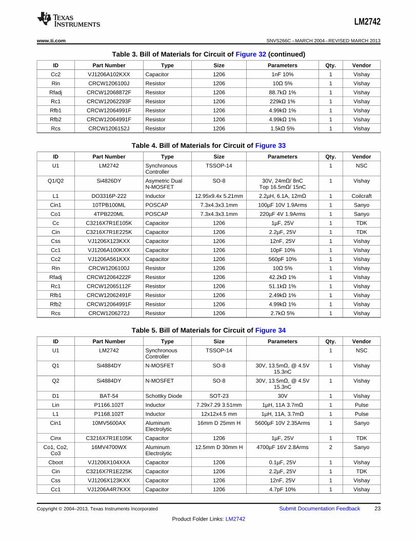
Table 3. Bill of Materials for Circuit of Figure 32 (continued)
ID Part Number Type Size Parameters Qty. Vendor
Cc2 VJ1206A102KXX Capacitor 1206 1nF 10% 1 Vishay
Rin CRCW1206100J Resistor 1206 10Ω 5% 1 Vishay
Rfadj CRCW12068872F Resistor 1206 88.7kΩ 1% 1 Vishay
Rc1 CRCW12062293F Resistor 1206 229kΩ 1% 1 Vishay
Rfb1 CRCW12064991F Resistor 1206 4.99kΩ 1% 1 Vishay
Rfb2 CRCW12064991F Resistor 1206 4.99kΩ 1% 1 Vishay
Rcs CRCW1206152J Resistor 1206 1.5kΩ 5% 1 Vishay
Table 4. Bill of Materials for Circuit of Figure 33
ID Part Number Type Size Parameters Qty. Vendor
U1 LM2742 Synchronous TSSOP-14 1 NSCController
Q1/Q2 Si4826DY Asymetric Dual SO-8 30V, 24mΩ/ 8nC 1 VishayN-MOSFET Top 16.5mΩ/ 15nC
L1 DO3316P-222 Inductor 12.95x9.4x 5.21mm 2.2µH, 6.1A, 12mΩ 1 Coilcraft
Cin1 10TPB100ML POSCAP 7.3x4.3x3.1mm 100µF 10V 1.9Arms 1 Sanyo
Co1 4TPB220ML POSCAP 7.3x4.3x3.1mm 220µF 4V 1.9Arms 1 Sanyo
Cc C3216X7R1E105K Capacitor 1206 1µF, 25V 1 TDK
Cin C3216X7R1E225K Capacitor 1206 2.2µF, 25V 1 TDK
Css VJ1206X123KXX Capacitor 1206 12nF, 25V 1 Vishay
Cc1 VJ1206A100KXX Capacitor 1206 10pF 10% 1 Vishay
Cc2 VJ1206A561KXX Capacitor 1206 560pF 10% 1 Vishay
Rin CRCW1206100J Resistor 1206 10Ω 5% 1 Vishay
Rfadj CRCW12064222F Resistor 1206 42.2kΩ 1% 1 Vishay
Rc1 CRCW12065112F Resistor 1206 51.1kΩ 1% 1 Vishay
Rfb1 CRCW12062491F Resistor 1206 2.49kΩ 1% 1 Vishay
Rfb2 CRCW12064991F Resistor 1206 4.99kΩ 1% 1 Vishay
Rcs CRCW1206272J Resistor 1206 2.7kΩ 5% 1 Vishay
Table 5. Bill of Materials for Circuit of Figure 34
ID Part Number Type Size Parameters Qty. Vendor
U1 LM2742 Synchronous TSSOP-14 1 NSCController
Q1 Si4884DY N-MOSFET SO-8 30V, 13.5mΩ, @ 4.5V 1 Vishay15.3nC
Q2 Si4884DY N-MOSFET SO-8 30V, 13.5mΩ, @ 4.5V 1 Vishay15.3nC
D1 BAT-54 Schottky Diode SOT-23 30V 1 Vishay
Lin P1166.102T Inductor 7.29x7.29 3.51mm 1µH, 11A 3.7mΩ 1 Pulse
L1 P1168.102T Inductor 12x12x4.5 mm 1µH, 11A, 3.7mΩ 1 Pulse
Cin1 10MV5600AX Aluminum 16mm D 25mm H 5600µF 10V 2.35Arms 1 SanyoElectrolytic
Cinx C3216X7R1E105K Capacitor 1206 1µF, 25V 1 TDK
Co1, Co2, 16MV4700WX Aluminum 12.5mm D 30mm H 4700µF 16V 2.8Arms 2 SanyoCo3 Electrolytic
Cboot VJ1206X104XXA Capacitor 1206 0.1µF, 25V 1 Vishay
Cin C3216X7R1E225K Capacitor 1206 2.2µF, 25V 1 TDK
Css VJ1206X123KXX Capacitor 1206 12nF, 25V 1 Vishay
Cc1 VJ1206A4R7KXX Capacitor 1206 4.7pF 10% 1 Vishay
Copyright © 2004–2013, Texas Instruments Incorporated Submit Documentation Feedback 23
Product Folder Links: LM2742
LM2742
SNVS266C –MARCH 2004–REVISED MARCH 2013 www.ti.com
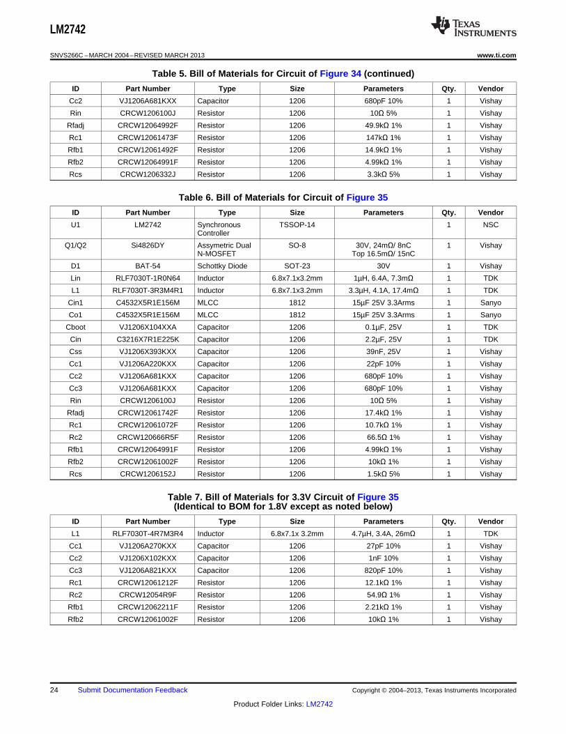
Table 5. Bill of Materials for Circuit of Figure 34 (continued)
ID Part Number Type Size Parameters Qty. Vendor
Cc2 VJ1206A681KXX Capacitor 1206 680pF 10% 1 Vishay
Rin CRCW1206100J Resistor 1206 10Ω 5% 1 Vishay
Rfadj CRCW12064992F Resistor 1206 49.9kΩ 1% 1 Vishay
Rc1 CRCW12061473F Resistor 1206 147kΩ 1% 1 Vishay
Rfb1 CRCW12061492F Resistor 1206 14.9kΩ 1% 1 Vishay
Rfb2 CRCW12064991F Resistor 1206 4.99kΩ 1% 1 Vishay
Rcs CRCW1206332J Resistor 1206 3.3kΩ 5% 1 Vishay
Table 6. Bill of Materials for Circuit of Figure 35
ID Part Number Type Size Parameters Qty. Vendor
U1 LM2742 Synchronous TSSOP-14 1 NSCController
Q1/Q2 Si4826DY Assymetric Dual SO-8 30V, 24mΩ/ 8nC 1 VishayN-MOSFET Top 16.5mΩ/ 15nC
D1 BAT-54 Schottky Diode SOT-23 30V 1 Vishay
Lin RLF7030T-1R0N64 Inductor 6.8x7.1x3.2mm 1µH, 6.4A, 7.3mΩ 1 TDK
L1 RLF7030T-3R3M4R1 Inductor 6.8x7.1x3.2mm 3.3µH, 4.1A, 17.4mΩ 1 TDK
Cin1 C4532X5R1E156M MLCC 1812 15µF 25V 3.3Arms 1 Sanyo
Co1 C4532X5R1E156M MLCC 1812 15µF 25V 3.3Arms 1 Sanyo
Cboot VJ1206X104XXA Capacitor 1206 0.1µF, 25V 1 TDK
Cin C3216X7R1E225K Capacitor 1206 2.2µF, 25V 1 TDK
Css VJ1206X393KXX Capacitor 1206 39nF, 25V 1 Vishay
Cc1 VJ1206A220KXX Capacitor 1206 22pF 10% 1 Vishay
Cc2 VJ1206A681KXX Capacitor 1206 680pF 10% 1 Vishay
Cc3 VJ1206A681KXX Capacitor 1206 680pF 10% 1 Vishay
Rin CRCW1206100J Resistor 1206 10Ω 5% 1 Vishay
Rfadj CRCW12061742F Resistor 1206 17.4kΩ 1% 1 Vishay
Rc1 CRCW12061072F Resistor 1206 10.7kΩ 1% 1 Vishay
Rc2 CRCW120666R5F Resistor 1206 66.5Ω 1% 1 Vishay
Rfb1 CRCW12064991F Resistor 1206 4.99kΩ 1% 1 Vishay
Rfb2 CRCW12061002F Resistor 1206 10kΩ 1% 1 Vishay
Rcs CRCW1206152J Resistor 1206 1.5kΩ 5% 1 Vishay
Table 7. Bill of Materials for 3.3V Circuit of Figure 35(Identical to BOM for 1.8V except as noted below)
ID Part Number Type Size Parameters Qty. Vendor
L1 RLF7030T-4R7M3R4 Inductor 6.8x7.1x 3.2mm 4.7µH, 3.4A, 26mΩ 1 TDK
Cc1 VJ1206A270KXX Capacitor 1206 27pF 10% 1 Vishay
Cc2 VJ1206X102KXX Capacitor 1206 1nF 10% 1 Vishay
Cc3 VJ1206A821KXX Capacitor 1206 820pF 10% 1 Vishay
Rc1 CRCW12061212F Resistor 1206 12.1kΩ 1% 1 Vishay
Rc2 CRCW12054R9F Resistor 1206 54.9Ω 1% 1 Vishay
Rfb1 CRCW12062211F Resistor 1206 2.21kΩ 1% 1 Vishay
Rfb2 CRCW12061002F Resistor 1206 10kΩ 1% 1 Vishay
24 Submit Documentation Feedback Copyright © 2004–2013, Texas Instruments Incorporated
Product Folder Links: LM2742
LM2742
www.ti.com SNVS266C –MARCH 2004–REVISED MARCH 2013
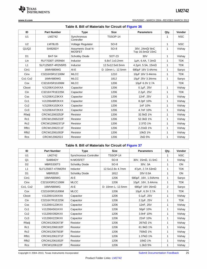
Table 8. Bill of Materials for Circuit of Figure 36
ID Part Number Type Size Parameters Qty. Vendor
U1 LM2742 Synchronous TSSOP-14 1 NSCController
U2 LM78L05 Voltage Regulator SO-8 1 NSC
Q1/Q2 Si4826DY Assymetric Dual N- SO-8 30V, 24mΩ/ 8nC 1 VishayMOSFET Top 16.5mΩ/ 15nC
D1 BAT-54 Schottky Diode SOT-23 30V 1 Vishay
Lin RLF7030T-1R0N64 Inductor 6.8x7.1x3.2mm 1µH, 6.4A, 7.3mΩ 1 TDK
L1 SLF12565T-4R2N5R5 Inductor 12.5x12.5x6.5mm 4.2µH, 5.5A, 15mΩ 1 TDK
Cin1 16MV680WG Al-E D: 10mm L: 12.5mm 680µF 16V 3.4Arms 1 Sanyo
Cinx C3216X5R1C106M MLCC 1210 10µF 16V 3.4Arms 1 TDK
Co1 Co2 16MV680WG MLCC 1812 15µF 25V 3.3Arms 1 Sanyo
Cox C3216X5R10J06M MLCC 1206 10µF 6.3V 2.7A TDK
Cboot VJ1206X104XXA Capacitor 1206 0.1µF, 25V 1 Vishay
Cin C3216X7R1E225K Capacitor 1206 2.2µF, 25V 1 TDK
Css VJ1206X123KXX Capacitor 1206 12nF, 25V 1 Vishay
Cc1 VJ1206A8R2KXX Capacitor 1206 8.2pF 10% 1 Vishay
Cc2 VJ1206X102KXX Capacitor 1206 1nF 10% 1 Vishay
Cc3 VJ1206X472KXX Capacitor 1206 4.7nF 10% 1 Vishay
Rfadj CRCW12063252F Resistor 1206 32.5kΩ 1% 1 Vishay
Rc1 CRCW12065232F Resistor 1206 52.3kΩ 1% 1 Vishay
Rc2 CRCW120662371F Resistor 1206 2.37Ω 1% 1 Vishay
Rfb1 CRCW12062211F Resistor 1206 2.21kΩ 1% 1 Vishay
Rfb2 CRCW12061002F Resistor 1206 10kΩ 1% 1 Vishay
Rcs CRCW1206202J Resistor 1206 2kΩ 5% 1 Vishay
Table 9. Bill of Materials for Circuit of Figure 37
ID Part Number Type Size Parameters Qty. Vendor
U1 LM2742 Synchronous Controller TSSOP-14 1 NSC
Q1 Si4894DY N-MOSFET SO-8 30V, 15mΩ, 11.5nC 1 Vishay
D2 MBRS330T3 Schottky Diode SO-8 30V, 3A 1 ON
L1 SLF12565T-470M2R4 Inductor 12.5x12.8x 4.7mm 47µH, 2.7A 53mΩ 1 TDK
D1 MBR0520 Schottky Diode 1812 20V 0.5A 1 ON
Cin1 16MV680WG Al-E 1206 680µF, 16V, 1.54Arms 1 Sanyo
Cinx C3216X5R1C106M MLCC 1206 10µF, 16V, 3.4Arms 1 TDK
Co1, Co2 16MV680WG Al-E D: 10mm L: 12.5mm 680µF 16V 26mΩ 2 Sanyo
Cox C3216X5R10J06M MLCC 1206 10µF, 6.3V 2.7A 1 TDK
Cboot VJ1206X104XXA Capacitor 1206 0.1µF, 25V 1 Vishay
Cin C3216X7R1E225K Capacitor 1206 2.2µF, 25V 1 TDK
Css VJ1206X123KXX Capacitor 1206 12nF, 25V 1 Vishay
Cc1 VJ1206A561KXX Capacitor 1206 56pF 10% 1 Vishay
Cc2 VJ1206X392KXX Capacitor 1206 3.9nF 10% 1 Vishay
Cc3 VJ1206X223KXX Capacitor 1206 22nF 10% 1 Vishay
Rfadj CRCW12062673F Resistor 1206 267kΩ 1% 1 Vishay
Rc1 CRCW12066192F Resistor 1206 61.9kΩ 1% 1 Vishay
Rc2 CRCW12067503F Resistor 1206 750kΩ 1% 1 Vishay
Rfb1 CRCW12061371F Resistor 1206 1.37kΩ 1% 1 Vishay
Rfb2 CRCW12061002F Resistor 1206 10kΩ 1% 1 Vishay
Rcs CRCW1206122F Resistor 1206 1.2kΩ 5% 1 Vishay
Copyright © 2004–2013, Texas Instruments Incorporated Submit Documentation Feedback 25
Product Folder Links: LM2742
LM2742
SNVS266C –MARCH 2004–REVISED MARCH 2013 www.ti.com
REVISION HISTORY
Changes from Revision B (March 2013) to Revision C Page
• Changed layout of National Data Sheet to TI format .......................................................................................................... 25
26 Submit Documentation Feedback Copyright © 2004–2013, Texas Instruments Incorporated
Product Folder Links: LM2742
PACKAGE OPTION ADDENDUM
www.ti.com 10-Sep-2014
Addendum-Page 1
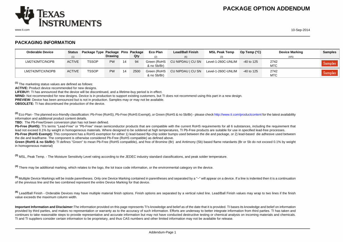
PACKAGING INFORMATION
Orderable Device Status(1)
Package Type PackageDrawing
Pins PackageQty
Eco Plan(2)
Lead/Ball Finish(6)
MSL Peak Temp(3)
Op Temp (°C) Device Marking(4/5)
Samples
LM2742MTC/NOPB ACTIVE TSSOP PW 14 94 Green (RoHS& no Sb/Br)
CU NIPDAU | CU SN Level-1-260C-UNLIM -40 to 125 2742MTC
LM2742MTCX/NOPB ACTIVE TSSOP PW 14 2500 Green (RoHS& no Sb/Br)
CU NIPDAU | CU SN Level-1-260C-UNLIM -40 to 125 2742MTC
(1) The marketing status values are defined as follows:ACTIVE: Product device recommended for new designs.LIFEBUY: TI has announced that the device will be discontinued, and a lifetime-buy period is in effect.NRND: Not recommended for new designs. Device is in production to support existing customers, but TI does not recommend using this part in a new design.PREVIEW: Device has been announced but is not in production. Samples may or may not be available.OBSOLETE: TI has discontinued the production of the device.
(2) Eco Plan - The planned eco-friendly classification: Pb-Free (RoHS), Pb-Free (RoHS Exempt), or Green (RoHS & no Sb/Br) - please check http://www.ti.com/productcontent for the latest availabilityinformation and additional product content details.TBD: The Pb-Free/Green conversion plan has not been defined.Pb-Free (RoHS): TI's terms "Lead-Free" or "Pb-Free" mean semiconductor products that are compatible with the current RoHS requirements for all 6 substances, including the requirement thatlead not exceed 0.1% by weight in homogeneous materials. Where designed to be soldered at high temperatures, TI Pb-Free products are suitable for use in specified lead-free processes.Pb-Free (RoHS Exempt): This component has a RoHS exemption for either 1) lead-based flip-chip solder bumps used between the die and package, or 2) lead-based die adhesive used betweenthe die and leadframe. The component is otherwise considered Pb-Free (RoHS compatible) as defined above.Green (RoHS & no Sb/Br): TI defines "Green" to mean Pb-Free (RoHS compatible), and free of Bromine (Br) and Antimony (Sb) based flame retardants (Br or Sb do not exceed 0.1% by weightin homogeneous material)
(3) MSL, Peak Temp. - The Moisture Sensitivity Level rating according to the JEDEC industry standard classifications, and peak solder temperature.
(4) There may be additional marking, which relates to the logo, the lot trace code information, or the environmental category on the device.
(5) Multiple Device Markings will be inside parentheses. Only one Device Marking contained in parentheses and separated by a "~" will appear on a device. If a line is indented then it is a continuationof the previous line and the two combined represent the entire Device Marking for that device.
(6) Lead/Ball Finish - Orderable Devices may have multiple material finish options. Finish options are separated by a vertical ruled line. Lead/Ball Finish values may wrap to two lines if the finishvalue exceeds the maximum column width.
Important Information and Disclaimer:The information provided on this page represents TI's knowledge and belief as of the date that it is provided. TI bases its knowledge and belief on informationprovided by third parties, and makes no representation or warranty as to the accuracy of such information. Efforts are underway to better integrate information from third parties. TI has taken andcontinues to take reasonable steps to provide representative and accurate information but may not have conducted destructive testing or chemical analysis on incoming materials and chemicals.TI and TI suppliers consider certain information to be proprietary, and thus CAS numbers and other limited information may not be available for release.
PACKAGE OPTION ADDENDUM
www.ti.com 10-Sep-2014
Addendum-Page 2
In no event shall TI's liability arising out of such information exceed the total purchase price of the TI part(s) at issue in this document sold by TI to Customer on an annual basis.
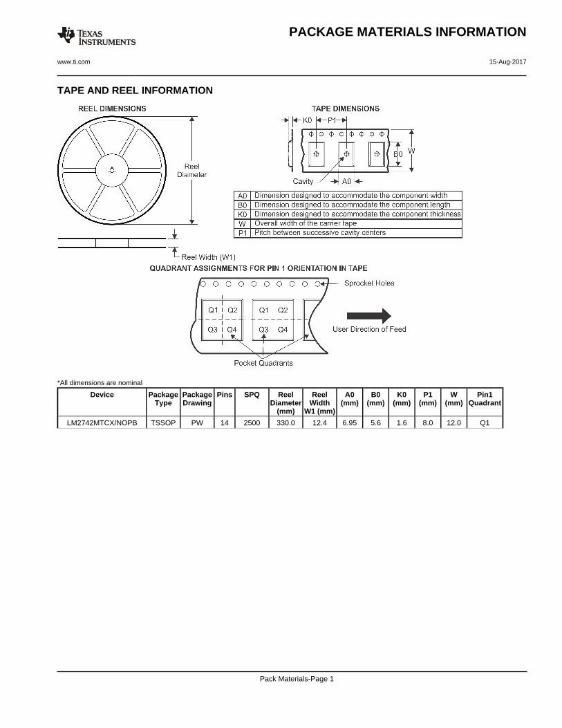
TAPE AND REEL INFORMATION
*All dimensions are nominal
Device PackageType
PackageDrawing
Pins SPQ ReelDiameter
(mm)
ReelWidth
W1 (mm)
A0(mm)
B0(mm)
K0(mm)
P1(mm)
W(mm)
Pin1Quadrant
LM2742MTCX/NOPB TSSOP PW 14 2500 330.0 12.4 6.95 5.6 1.6 8.0 12.0 Q1
PACKAGE MATERIALS INFORMATION
www.ti.com 15-Aug-2017
Pack Materials-Page 1
*All dimensions are nominal
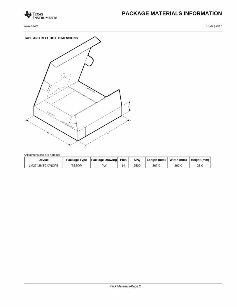
Device Package Type Package Drawing Pins SPQ Length (mm) Width (mm) Height (mm)
LM2742MTCX/NOPB TSSOP PW 14 2500 367.0 367.0 35.0
PACKAGE MATERIALS INFORMATION
www.ti.com 15-Aug-2017
Pack Materials-Page 2
IMPORTANT NOTICE
Texas Instruments Incorporated (TI) reserves the right to make corrections, enhancements, improvements and other changes to itssemiconductor products and services per JESD46, latest issue, and to discontinue any product or service per JESD48, latest issue. Buyersshould obtain the latest relevant information before placing orders and should verify that such information is current and complete.TI’s published terms of sale for semiconductor products (http://www.ti.com/sc/docs/stdterms.htm) apply to the sale of packaged integratedcircuit products that TI has qualified and released to market. Additional terms may apply to the use or sale of other types of TI products andservices.Reproduction of significant portions of TI information in TI data sheets is permissible only if reproduction is without alteration and isaccompanied by all associated warranties, conditions, limitations, and notices. TI is not responsible or liable for such reproduceddocumentation. Information of third parties may be subject to additional restrictions. Resale of TI products or services with statementsdifferent from or beyond the parameters stated by TI for that product or service voids all express and any implied warranties for theassociated TI product or service and is an unfair and deceptive business practice. TI is not responsible or liable for any such statements.Buyers and others who are developing systems that incorporate TI products (collectively, “Designers”) understand and agree that Designersremain responsible for using their independent analysis, evaluation and judgment in designing their applications and that Designers havefull and exclusive responsibility to assure the safety of Designers' applications and compliance of their applications (and of all TI productsused in or for Designers’ applications) with all applicable regulations, laws and other applicable requirements. Designer represents that, withrespect to their applications, Designer has all the necessary expertise to create and implement safeguards that (1) anticipate dangerousconsequences of failures, (2) monitor failures and their consequences, and (3) lessen the likelihood of failures that might cause harm andtake appropriate actions. Designer agrees that prior to using or distributing any applications that include TI products, Designer willthoroughly test such applications and the functionality of such TI products as used in such applications.TI’s provision of technical, application or other design advice, quality characterization, reliability data or other services or information,including, but not limited to, reference designs and materials relating to evaluation modules, (collectively, “TI Resources”) are intended toassist designers who are developing applications that incorporate TI products; by downloading, accessing or using TI Resources in anyway, Designer (individually or, if Designer is acting on behalf of a company, Designer’s company) agrees to use any particular TI Resourcesolely for this purpose and subject to the terms of this Notice.TI’s provision of TI Resources does not expand or otherwise alter TI’s applicable published warranties or warranty disclaimers for TIproducts, and no additional obligations or liabilities arise from TI providing such TI Resources. TI reserves the right to make corrections,enhancements, improvements and other changes to its TI Resources. TI has not conducted any testing other than that specificallydescribed in the published documentation for a particular TI Resource.Designer is authorized to use, copy and modify any individual TI Resource only in connection with the development of applications thatinclude the TI product(s) identified in such TI Resource. NO OTHER LICENSE, EXPRESS OR IMPLIED, BY ESTOPPEL OR OTHERWISETO ANY OTHER TI INTELLECTUAL PROPERTY RIGHT, AND NO LICENSE TO ANY TECHNOLOGY OR INTELLECTUAL PROPERTYRIGHT OF TI OR ANY THIRD PARTY IS GRANTED HEREIN, including but not limited to any patent right, copyright, mask work right, orother intellectual property right relating to any combination, machine, or process in which TI products or services are used. Informationregarding or referencing third-party products or services does not constitute a license to use such products or services, or a warranty orendorsement thereof. Use of TI Resources may require a license from a third party under the patents or other intellectual property of thethird party, or a license from TI under the patents or other intellectual property of TI.TI RESOURCES ARE PROVIDED “AS IS” AND WITH ALL FAULTS. TI DISCLAIMS ALL OTHER WARRANTIES ORREPRESENTATIONS, EXPRESS OR IMPLIED, REGARDING RESOURCES OR USE THEREOF, INCLUDING BUT NOT LIMITED TOACCURACY OR COMPLETENESS, TITLE, ANY EPIDEMIC FAILURE WARRANTY AND ANY IMPLIED WARRANTIES OFMERCHANTABILITY, FITNESS FOR A PARTICULAR PURPOSE, AND NON-INFRINGEMENT OF ANY THIRD PARTY INTELLECTUALPROPERTY RIGHTS. TI SHALL NOT BE LIABLE FOR AND SHALL NOT DEFEND OR INDEMNIFY DESIGNER AGAINST ANY CLAIM,INCLUDING BUT NOT LIMITED TO ANY INFRINGEMENT CLAIM THAT RELATES TO OR IS BASED ON ANY COMBINATION OFPRODUCTS EVEN IF DESCRIBED IN TI RESOURCES OR OTHERWISE. IN NO EVENT SHALL TI BE LIABLE FOR ANY ACTUAL,DIRECT, SPECIAL, COLLATERAL, INDIRECT, PUNITIVE, INCIDENTAL, CONSEQUENTIAL OR EXEMPLARY DAMAGES INCONNECTION WITH OR ARISING OUT OF TI RESOURCES OR USE THEREOF, AND REGARDLESS OF WHETHER TI HAS BEENADVISED OF THE POSSIBILITY OF SUCH DAMAGES.Unless TI has explicitly designated an individual product as meeting the requirements of a particular industry standard (e.g., ISO/TS 16949and ISO 26262), TI is not responsible for any failure to meet such industry standard requirements.Where TI specifically promotes products as facilitating functional safety or as compliant with industry functional safety standards, suchproducts are intended to help enable customers to design and create their own applications that meet applicable functional safety standardsand requirements. Using products in an application does not by itself establish any safety features in the application. Designers mustensure compliance with safety-related requirements and standards applicable to their applications. Designer may not use any TI products inlife-critical medical equipment unless authorized officers of the parties have executed a special contract specifically governing such use.Life-critical medical equipment is medical equipment where failure of such equipment would cause serious bodily injury or death (e.g., lifesupport, pacemakers, defibrillators, heart pumps, neurostimulators, and implantables). Such equipment includes, without limitation, allmedical devices identified by the U.S. Food and Drug Administration as Class III devices and equivalent classifications outside the U.S.TI may expressly designate certain products as completing a particular qualification (e.g., Q100, Military Grade, or Enhanced Product).Designers agree that it has the necessary expertise to select the product with the appropriate qualification designation for their applicationsand that proper product selection is at Designers’ own risk. Designers are solely responsible for compliance with all legal and regulatoryrequirements in connection with such selection.Designer will fully indemnify TI and its representatives against any damages, costs, losses, and/or liabilities arising out of Designer’s non-compliance with the terms and provisions of this Notice.
Mailing Address: Texas Instruments, Post Office Box 655303, Dallas, Texas 75265Copyright © 2017, Texas Instruments Incorporated