
LM2738 550kHz/1.6MHz 1.5A Step-Down DC-DC...
28
April 10, 2008 LM2738 550kHz/1.6MHz 1.5A Step-Down DC-DC Switching Regulator General Description The LM2738 regulator is a monolithic, high frequency, PWM step-down DC/DC converter in an 8-pin LLP or 8-pin eMSOP package. It provides all the active functions for local DC/DC conversion with fast transient response and accurate regula- tion in the smallest possible PCB area. With a minimum of external components, the LM2738 is easy to use. The ability to drive 1.5A loads with an internal 250mΩ NMOS switch using state-of-the-art 0.5µm BiCMOS technology results in the best power density available. Switching frequency is internally set to 550kHz (LM2738Y) or 1.6MHz (LM2738X), allowing the use of extremely small sur- face mount inductors and chip capacitors. Even though the operating frequencies are very high, efficiencies up to 90% are easy to achieve. External enable is included, featuring an ultra-low stand-by current of 400nA. The LM2738 utilizes cur- rent-mode control and internal compensation to provide high- performance regulation over a wide range of operating conditions. Additional features include internal soft-start cir- cuitry to reduce in-rush current, cycle-by-cycle current limit, thermal shutdown, and output over-voltage protection. Features ■ Space Saving LLP-8 and eMSOP-8 package ■ 3.0V to 20V input voltage range ■ 0.8V to 18V output voltage range ■ 1.5A output current ■ 550kHz (LM2738Y) and 1.6MHz (LM2738X) switching frequencies ■ 250mΩ NMOS switch ■ 400nA shutdown current ■ 0.8V, 2% internal voltage reference ■ Internal soft-start ■ Current-Mode, PWM operation ■ Thermal shutdown Applications ■ Local Point of Load Regulation ■ Core Power in HDDs ■ Set-Top Boxes ■ Battery Powered Devices ■ USB Powered Devices ■ DSL Modems Typical Application Circuit 30049101 Efficiency vs Load Current V IN = 12V, V OUT = 3.3V 30049145 © 2008 National Semiconductor Corporation 300491 www.national.com LM2738 550kHz/1.6MHz 1.5A Step-Down DC-DC Switching Regulator
Transcript of LM2738 550kHz/1.6MHz 1.5A Step-Down DC-DC...

April 10, 2008
LM2738550kHz/1.6MHz 1.5A Step-Down DC-DC SwitchingRegulatorGeneral DescriptionThe LM2738 regulator is a monolithic, high frequency, PWMstep-down DC/DC converter in an 8-pin LLP or 8-pin eMSOPpackage. It provides all the active functions for local DC/DCconversion with fast transient response and accurate regula-tion in the smallest possible PCB area.
With a minimum of external components, the LM2738 is easyto use. The ability to drive 1.5A loads with an internal250mΩ NMOS switch using state-of-the-art 0.5µm BiCMOStechnology results in the best power density available.Switching frequency is internally set to 550kHz (LM2738Y) or1.6MHz (LM2738X), allowing the use of extremely small sur-face mount inductors and chip capacitors. Even though theoperating frequencies are very high, efficiencies up to 90%are easy to achieve. External enable is included, featuring anultra-low stand-by current of 400nA. The LM2738 utilizes cur-rent-mode control and internal compensation to provide high-performance regulation over a wide range of operatingconditions. Additional features include internal soft-start cir-cuitry to reduce in-rush current, cycle-by-cycle current limit,thermal shutdown, and output over-voltage protection.
Features Space Saving LLP-8 and eMSOP-8 package
3.0V to 20V input voltage range
0.8V to 18V output voltage range
1.5A output current
550kHz (LM2738Y) and 1.6MHz (LM2738X)switching frequencies
250mΩ NMOS switch
400nA shutdown current
0.8V, 2% internal voltage reference
Internal soft-start
Current-Mode, PWM operation
Thermal shutdown
Applications Local Point of Load Regulation
Core Power in HDDs
Set-Top Boxes
Battery Powered Devices
USB Powered Devices
DSL Modems
Typical Application Circuit
30049101
Efficiency vs Load CurrentVIN = 12V, VOUT = 3.3V
30049145
© 2008 National Semiconductor Corporation 300491 www.national.com
LM
2738 5
50kH
z/1.6
MH
z 1.5
A S
tep
-Do
wn
DC
-DC
Sw
itch
ing
Reg
ula
tor

Connection Diagrams
30049161
8-Pin LLP - TOP VIEWNS Package Number SDA08A
30049163
8-Pin eMSOP - TOP VIEWNS Package Number MUY08A
Ordering Information
Order Number Frequency
Option
Package Type NSC Package
Drawing
Package Marking Supplied As
LM2738XSD1.6MHz
8-Lead LLP SDA08A
L237B1000 Tape and Reel
LM2738XSDX 4500 Tape and Reel
LM2738YSD0.55MHz L174B
1000 Tape and Reel
LM2738YSDX 4500 Tape and Reel
LM2738XMY1.6MHz
8-Lead eMSOP MUY08A
STDB1000 Tape and Reel
LM2738XMYX 3500 Tape and Reel
LM2738YMY0.55MHz SJBB
1000 Tape and Reel
LM2738YMYX 3500 Tape and Reel
* Contact the local sales office for the lead-free package.
Pin Descriptions
Pin Name Function
1 BOOSTBoost voltage that drives the internal NMOS control switch. A
bootstrap capacitor is connected between the BOOST and SW pins.
2 VIN
Supply voltage for output power stage. Connect a bypass capacitor
to this pin. Must tie pins 2 and 3 together at package.
3 VCC
Input supply voltage of the IC. Connect a bypass capacitor to this pin.
Must tie pin 2 and 3 together at the package.
4 ENEnable control input. Logic high enables operation. Do not allow this
pin to float or be greater than VIN + 0.3V.
5, 7 GNDSignal and power ground pins. Place the bottom resistor of the
feedback network as close as possible to these pins.
6FB Feedback pin. Connect FB to the external resistor divider to set output
voltage.
8 SWOutput switch. Connects to the inductor, catch diode, and bootstrap
capacitor.
DAP GND Signal and power ground. Must be connected to GND on the PCB.
www.national.com 2
LM
2738

Absolute Maximum Ratings (Note 1)
If Military/Aerospace specified devices are required,please contact the National Semiconductor Sales Office/Distributors for availability and specifications.
VIN, VCC -0.5V to 24V
SW Voltage -0.5V to 24V
Boost Voltage -0.5V to 30V
Boost to SW Voltage -0.5V to 6.0V
FB Voltage -0.5V to 3.0V
EN Voltage -0.5V to (VIN + 0.3V)
Junction Temperature 150°C
ESD Susceptibility (Note 2) 2kV
Storage Temp. Range -65°C to 150°C
Soldering Information
Infrared/Convection Reflow (15sec) 220°C
Wave Soldering Lead Temp. (10sec) 260°C
Operating Ratings (Note 1)
VIN, VCC 3V to 20V
SW Voltage -0.5V to 20V
Boost Voltage -0.5V to 25.5V
Boost to SW Voltage 2.5V to 5.5V
Junction Temperature Range −40°C to +125°C
Thermal Resistance θJA for LLP/eMSOP(Note 3) 60°C/W
Thermal Shutdown (Note 3) 165°C
Electrical CharacteristicsSpecifications with standard typeface are for TJ = 25°C, and those in boldface type apply over the full Operating TemperatureRange (TJ = -40°C to 125°C). VIN = 12V, VBOOST - VSW = 5V unless otherwise specified. Datasheet min/max specification limitsare guaranteed by design, test, or statistical analysis.
Symbol Parameter ConditionsMin
(Note 4)
Typ
(Note 5)
Max
(Note 4)Units
VFB Feedback Voltage 0.784 0.800 0.816 V
ΔVFB/ΔVIN Feedback Voltage Line Regulation VIN = 3V to 20V 0.02 % / V
IFB Feedback Input Bias Current Sink/Source 0.1 100 nA
UVLO
Undervoltage Lockout VIN Rising 2.7 2.90
VUndervoltage Lockout VIN Falling 2.0 2.3
UVLO Hysteresis 0.4
FSW Switching FrequencyLM2738X 1.28 1.6 1.92
MHzLM2738Y 0.364 0.55 0.676
DMAX Maximum Duty CycleLM2738X , Load=150mA 92
%LM2738Y, Load=150mA 95
DMIN Minimum Duty CycleLM2738X 7.5
%LM2738Y 2
RDS(ON) Switch ON ResistanceVBOOST - VSW = 3V,
Load=400mA
250 500 mΩ
ICL Switch Current Limit VBOOST - VSW = 3V, VIN = 3V 2.0 2.9 A
IQQuiescent Current
Switching 1.9 3 mA
Non-Switching 1.9 mA
Quiescent Current (shutdown) VEN = 0V 400 nA
IBOOST Boost Pin CurrentLM2738X (27% Duty Cycle) 4.5
mALM2738Y (27% Duty Cycle) 2.5
VEN_TH
Shutdown Threshold Voltage VEN Falling - 0.4V
Enable Threshold Voltage VEN Rising 1.4 -
IEN Enable Pin Current Sink/Source 10 nA
ISW Switch Leakage VIN = 20V 100 nA
Note 1: Absolute Maximum Ratings indicate limits beyond which damage to the device may occur. Operating Ratings indicate conditions for which the device isintended to be functional, but specific performance is not guaranteed. For guaranteed specifications and the test conditions, see Electrical Characteristics.
Note 2: Human body model, 1.5kΩ in series with 100pF.
Note 3: Typical thermal shutdown will occur if the junction temperature exceeds 165°C. The maximum power dissipation is a function of TJ(MAX) , θJA and TA .The maximum allowable power dissipation at any ambient temperature is PD = (TJ(MAX) – TA)/θJA . All numbers apply for packages soldered directly onto a 3” x3” PC board with 2 oz. copper on 4 layers in still air in accordance to JEDEC standards. Thermal resistance varies greatly with layout, copper thicknes, numberof layers in PCB, power distribution, number of thermal vias, board size, ambient temperature, and air flow.
Note 4: Guaranteed to National’s Average Outgoing Quality Level (AOQL).
Note 5: Typicals represent the most likely parametric norm.
3 www.national.com
LM
2738
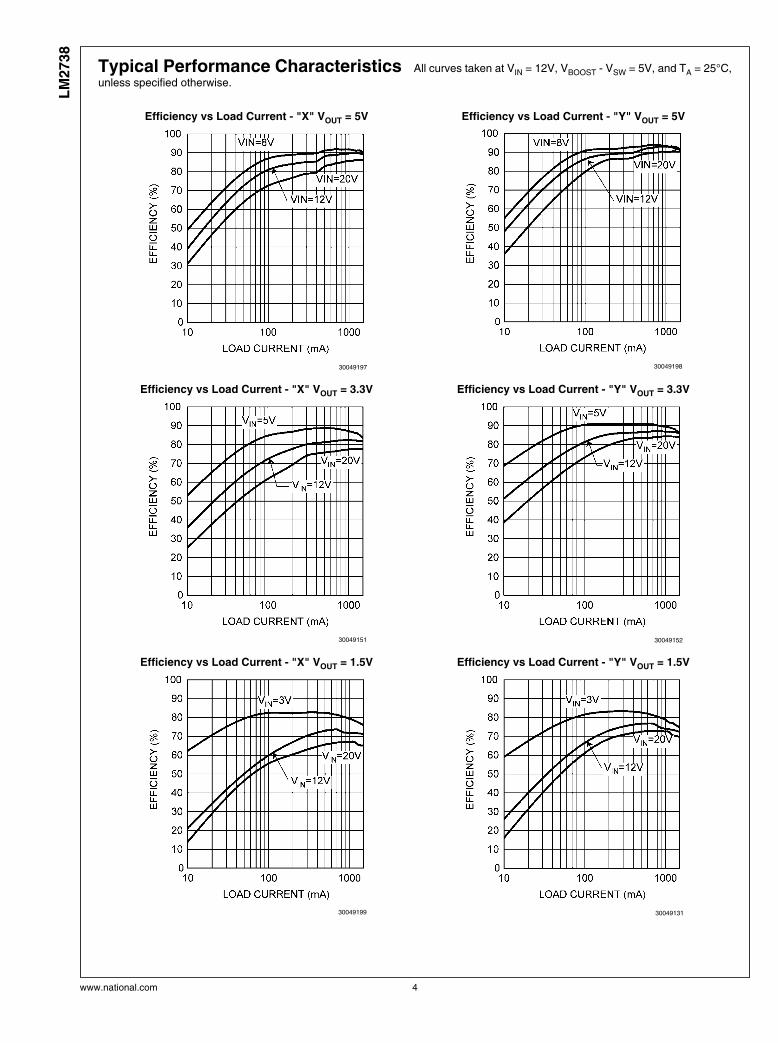
Typical Performance Characteristics All curves taken at VIN = 12V, VBOOST - VSW = 5V, and TA = 25°C,
unless specified otherwise.
Efficiency vs Load Current - "X" VOUT = 5V
30049197
Efficiency vs Load Current - "Y" VOUT = 5V
30049198
Efficiency vs Load Current - "X" VOUT = 3.3V
30049151
Efficiency vs Load Current - "Y" VOUT = 3.3V
30049152
Efficiency vs Load Current - "X" VOUT = 1.5V
30049199
Efficiency vs Load Current - "Y" VOUT = 1.5V
30049131
www.national.com 4
LM
2738

Typical Performance Characteristics All curves taken at VIN = 12V, VBOOST - VSW = 5V, and TA = 25°C,
unless specified otherwise.
Oscillator Frequency vs Temperature - "X"
30049127
Oscillator Frequency vs Temperature - "Y"
30049128
Current Limit vs TemperatureVIN = 5V
30049129
IQ Non-Switching vs Temperature
30049147
VFB vs Temperature
30049133
RDSON vs Temperature
30049130
5 www.national.com
LM
2738
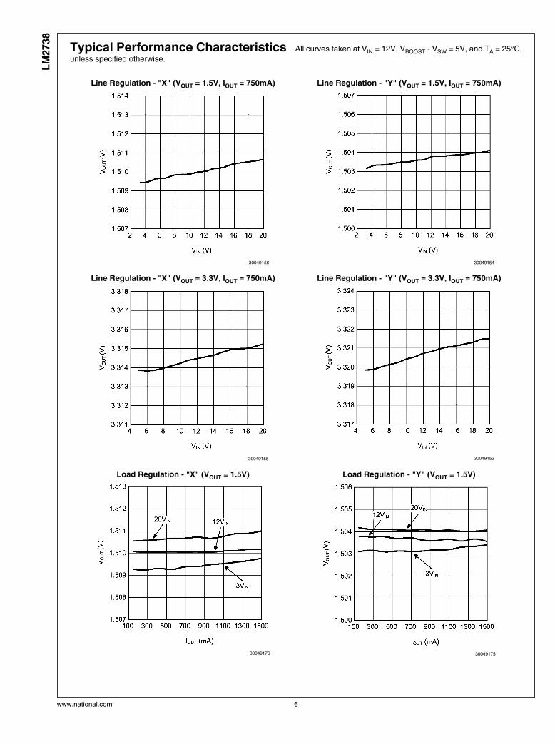
Typical Performance Characteristics All curves taken at VIN = 12V, VBOOST - VSW = 5V, and TA = 25°C,
unless specified otherwise.
Line Regulation - "X" (VOUT = 1.5V, IOUT = 750mA)
30049156
Line Regulation - "Y" (VOUT = 1.5V, IOUT = 750mA)
30049154
Line Regulation - "X" (VOUT = 3.3V, IOUT = 750mA)
30049155
Line Regulation - "Y" (VOUT = 3.3V, IOUT = 750mA)
30049153
Load Regulation - "X" (VOUT = 1.5V)
30049176
Load Regulation - "Y" (VOUT = 1.5V)
30049175
www.national.com 6
LM
2738
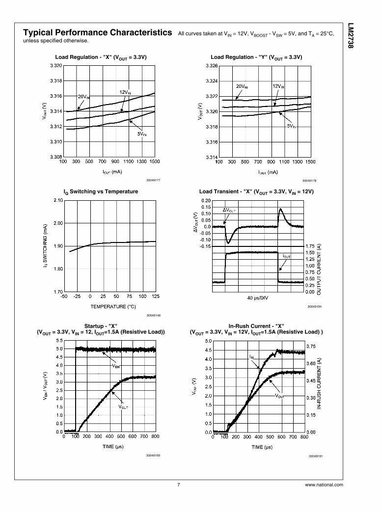
Typical Performance Characteristics All curves taken at VIN = 12V, VBOOST - VSW = 5V, and TA = 25°C,
unless specified otherwise.
Load Regulation - "X" (VOUT = 3.3V)
30049177
Load Regulation - "Y" (VOUT = 3.3V)
30049178
IQ Switching vs Temperature
30049146
Load Transient - "X" (VOUT = 3.3V, VIN = 12V)
30049194
Startup - "X"(VOUT = 3.3V, VIN = 12, IOUT=1.5A (Resistive Load))
30049190
In-Rush Current - "X"(VOUT = 3.3V, VIN = 12V, IOUT=1.5A (Resistive Load) )
30049191
7 www.national.com
LM
2738

Block Diagram
30049106
FIGURE 1. Simplified Internal Block Diagram
Application Information
THEORY OF OPERATION
The LM2738 is a constant frequency PWM buck regulator ICthat delivers a 1.5A load current. The regulator has a presetswitching frequency of either 550kHz (LM2738Y) or 1.6MHz(LM2738X). These high frequencies allow the LM2738 to op-erate with small surface mount capacitors and inductors,resulting in DC/DC converters that require a minimum amountof board space. The LM2738 is internally compensated, so itis simple to use, and requires few external components. TheLM2738 uses current-mode control to regulate the outputvoltage.
The following operating description of the LM2738 will referto the Simplified Block Diagram (Figure 1) and to the wave-forms in Figure 2. The LM2738 supplies a regulated outputvoltage by switching the internal NMOS control switch at con-stant frequency and variable duty cycle. A switching cyclebegins at the falling edge of the reset pulse generated by theinternal oscillator. When this pulse goes low, the output con-trol logic turns on the internal NMOS control switch. Duringthis on-time, the SW pin voltage (VSW) swings up to approxi-mately VIN, and the inductor current (IL) increases with a linearslope. IL is measured by the current-sense amplifier, whichgenerates an output proportional to the switch current. Thesense signal is summed with the regulator’s corrective rampand compared to the error amplifier’s output, which is propor-tional to the difference between the feedback voltage andVREF. When the PWM comparator output goes high, the out-put switch turns off until the next switching cycle begins.During the switch off-time, inductor current dischargesthrough Schottky diode D1, which forces the SW pin to swing
below ground by the forward voltage (VD) of the catch diode.The regulator loop adjusts the duty cycle (D) to maintain aconstant output voltage.
30049107
FIGURE 2. LM2738 Waveforms of SW Pin Voltage andInductor Current
BOOST FUNCTION
Capacitor CBOOST and diode D2 in Figure 3 are used to gen-erate a voltage VBOOST. VBOOST - VSW is the gate drive voltageto the internal NMOS control switch. To properly drive the in-ternal NMOS switch during its on-time, VBOOST needs to be atleast 2.5V greater than VSW. It is recommended that VBOOSTbe greater than 2.5V above VSW for best efficiency. VBOOST –VSW should not exceed the maximum operating limit of 5.5V.
www.national.com 8
LM
2738

5.5V > VBOOST – VSW > 2.5V for best performance.
When the LM2738 starts up, internal circuitry from theBOOST pin supplies a maximum of 20mA to CBOOST. Thiscurrent charges CBOOST to a voltage sufficient to turn theswitch on. The BOOST pin will continue to source current toCBOOST until the voltage at the feedback pin is greater than0.76V.
There are various methods to derive VBOOST:
1. From the input voltage (3.0V < VIN < 5.5V)
2. From the output voltage (2.5V < VOUT < 5.5V)
3. From an external distributed voltage rail (2.5V < VEXT <5.5V)
4. From a shunt or series zener diode
In the Simplifed Block Diagram of Figure 1, capacitorCBOOST and diode D2 supply the gate-drive voltage for theNMOS switch. Capacitor CBOOST is charged via diode D2 byVIN. During a normal switching cycle, when the internal NMOScontrol switch is off (TOFF) (refer to Figure 2), VBOOST equalsVIN minus the forward voltage of D2 (VFD2), during which thecurrent in the inductor (L) forward biases the Schottky diodeD1 (VFD1). Therefore the voltage stored across CBOOST is
VBOOST - VSW = VIN - VFD2 + VFD1
When the NMOS switch turns on (TON), the switch pin risesto
VSW = VIN – (RDSON x IL),
forcing VBOOST to rise thus reverse biasing D2. The voltage atVBOOST is then
VBOOST = 2VIN – (RDSON x IL) – VFD2 + VFD1
which is approximately
2VIN - 0.4V
for many applications. Thus the gate-drive voltage of theNMOS switch is approximately
VIN - 0.2V
An alternate method for charging CBOOST is to connect D2 tothe output as shown in Figure 3. The output voltage shouldbe between 2.5V and 5.5V, so that proper gate voltage will beapplied to the internal switch. In this circuit, CBOOST providesa gate drive voltage that is slightly less than VOUT.
30049108
FIGURE 3. VOUT Charges CBOOST
In applications where both VIN and VOUT are greater than5.5V, or less than 3V, CBOOST cannot be charged directly fromthese voltages. If VIN and VOUT are greater than 5.5V,CBOOST can be charged from VIN or VOUT minus a zener volt-age by placing a zener diode D3 in series with D2, as shownin Figure 4. When using a series zener diode from the input,ensure that the regulation of the input supply doesn’t createa voltage that falls outside the recommended VBOOST voltage.
(VINMAX – VD3) < 5.5V
(VINMIN – VD3) > 2.5V
30049109
FIGURE 4. Zener Reduces Boost Voltage from VIN
An alternative method is to place the zener diode D3 in ashunt configuration as shown in Figure 5. A small 350mW to500mW 5.1V zener in a SOT-23 or SOD package can be usedfor this purpose. A small ceramic capacitor such as a 6.3V,0.1µF capacitor (C4) should be placed in parallel with thezener diode. When the internal NMOS switch turns on, a pulseof current is drawn to charge the internal NMOS gate capac-itance. The 0.1 µF parallel shunt capacitor ensures that theVBOOST voltage is maintained during this time.
30049148
FIGURE 5. Boost Voltage Supplied from the Shunt Zeneron VIN
Resistor R3 should be chosen to provide enough RMS currentto the zener diode (D3) and to the BOOST pin. A recom-mended choice for the zener current (IZENER) is 1 mA. Thecurrent IBOOST into the BOOST pin supplies the gate currentof the NMOS control switch and varies typically according tothe following formula for the X version:
IBOOST = 0.56 x (D + 0.54) x (VZENER – VD2) mA
IBOOST can be calculated for the Y version using the following:
IBOOST = 0.22 x (D + 0.54) x (VZENER - VD2) µA
where D is the duty cycle, VZENER and VD2 are in volts, andIBOOST is in milliamps. VZENER is the voltage applied to theanode of the boost diode (D2), and VD2 is the average forwardvoltage across D2. Note that this formula for IBOOST gives typ-ical current. For the worst case IBOOST, increase the currentby 40%. In that case, the worst case boost current will be
IBOOST-MAX = 1.4 x IBOOST
R3 will then be given by
R3 = (VIN - VZENER) / (1.4 x IBOOST + IZENER)
9 www.national.com
LM
2738
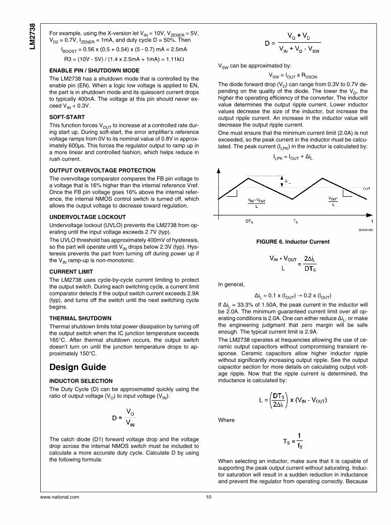
For example, using the X-version let VIN = 10V, VZENER = 5V,VD2 = 0.7V, IZENER = 1mA, and duty cycle D = 50%. Then
IBOOST = 0.56 x (0.5 + 0.54) x (5 - 0.7) mA = 2.5mA
R3 = (10V - 5V) / (1.4 x 2.5mA + 1mA) = 1.11kΩ
ENABLE PIN / SHUTDOWN MODE
The LM2738 has a shutdown mode that is controlled by theenable pin (EN). When a logic low voltage is applied to EN,the part is in shutdown mode and its quiescent current dropsto typically 400nA. The voltage at this pin should never ex-ceed VIN + 0.3V.
SOFT-START
This function forces VOUT to increase at a controlled rate dur-ing start up. During soft-start, the error amplifier’s referencevoltage ramps from 0V to its nominal value of 0.8V in approx-imately 600µs. This forces the regulator output to ramp up ina more linear and controlled fashion, which helps reduce inrush current.
OUTPUT OVERVOLTAGE PROTECTION
The overvoltage comparator compares the FB pin voltage toa voltage that is 16% higher than the internal reference Vref.Once the FB pin voltage goes 16% above the internal refer-ence, the internal NMOS control switch is turned off, whichallows the output voltage to decrease toward regulation.
UNDERVOLTAGE LOCKOUT
Undervoltage lockout (UVLO) prevents the LM2738 from op-erating until the input voltage exceeds 2.7V (typ).
The UVLO threshold has approximately 400mV of hysteresis,so the part will operate until VIN drops below 2.3V (typ). Hys-teresis prevents the part from turning off during power up ifthe VIN ramp-up is non-monotonic.
CURRENT LIMIT
The LM2738 uses cycle-by-cycle current limiting to protectthe output switch. During each switching cycle, a current limitcomparator detects if the output switch current exceeds 2.9A(typ), and turns off the switch until the next switching cyclebegins.
THERMAL SHUTDOWN
Thermal shutdown limits total power dissipation by turning offthe output switch when the IC junction temperature exceeds165°C. After thermal shutdown occurs, the output switchdoesn’t turn on until the junction temperature drops to ap-proximately 150°C.
Design Guide
INDUCTOR SELECTION
The Duty Cycle (D) can be approximated quickly using theratio of output voltage (VO) to input voltage (VIN):
The catch diode (D1) forward voltage drop and the voltagedrop across the internal NMOS switch must be included tocalculate a more accurate duty cycle. Calculate D by usingthe following formula:
VSW can be approximated by:
VSW = IOUT x RDSON
The diode forward drop (VD) can range from 0.3V to 0.7V de-pending on the quality of the diode. The lower the VD, thehigher the operating efficiency of the converter. The inductorvalue determines the output ripple current. Lower inductorvalues decrease the size of the inductor, but increase theoutput ripple current. An increase in the inductor value willdecrease the output ripple current.
One must ensure that the minimum current limit (2.0A) is notexceeded, so the peak current in the inductor must be calcu-lated. The peak current (ILPK) in the inductor is calculated by:
ILPK = IOUT + ΔiL
30049180
FIGURE 6. Inductor Current
In general,
ΔiL = 0.1 x (IOUT) → 0.2 x (IOUT)
If ΔiL = 33.3% of 1.50A, the peak current in the inductor willbe 2.0A. The minimum guaranteed current limit over all op-erating conditions is 2.0A. One can either reduce ΔiL, or makethe engineering judgment that zero margin will be safeenough. The typical current limit is 2.9A.
The LM2738 operates at frequencies allowing the use of ce-ramic output capacitors without compromising transient re-sponse. Ceramic capacitors allow higher inductor ripplewithout significantly increasing output ripple. See the outputcapacitor section for more details on calculating output volt-age ripple. Now that the ripple current is determined, theinductance is calculated by:
Where
When selecting an inductor, make sure that it is capable ofsupporting the peak output current without saturating. Induc-tor saturation will result in a sudden reduction in inductanceand prevent the regulator from operating correctly. Because
www.national.com 10
LM
2738
of the speed of the internal current limit, the peak current ofthe inductor need only be specified for the required maximumoutput current. For example, if the designed maximum outputcurrent is 1.0A and the peak current is 1.25A, then the induc-tor should be specified with a saturation current limit of >1.25A. There is no need to specify the saturation or peak cur-rent of the inductor at the 2.9A typical switch current limit.Because of the operating frequency of the LM2738, ferritebased inductors are preferred to minimize core losses. Thispresents little restriction since the variety of ferrite-based in-ductors is huge. Lastly, inductors with lower series resistance(RDCR) will provide better operating efficiency. For recom-mended inductors see Example Circuits.
INPUT CAPACITOR
An input capacitor is necessary to ensure that VIN does notdrop excessively during switching transients. The primaryspecifications of the input capacitor are capacitance, voltage,RMS current rating, and ESL (Equivalent Series Inductance).The recommended input capacitance is 10 µF.The input volt-age rating is specifically stated by the capacitor manufacturer.Make sure to check any recommended deratings and alsoverify if there is any significant change in capacitance at theoperating input voltage and the operating temperature. Theinput capacitor maximum RMS input current rating (IRMS-IN)must be greater than:
Neglecting inductor ripple simplifies the above equation to:
It can be shown from the above equation that maximum RMScapacitor current occurs when D = 0.5. Always calculate theRMS at the point where the duty cycle D is closest to 0.5. TheESL of an input capacitor is usually determined by the effec-tive cross sectional area of the current path. A large leadedcapacitor will have high ESL and a 0805 ceramic chip capac-itor will have very low ESL. At the operating frequencies of theLM2738, leaded capacitors may have an ESL so large thatthe resulting impedance (2πfL) will be higher than that re-quired to provide stable operation. As a result, surface mountcapacitors are strongly recommended.
Sanyo POSCAP, Tantalum or Niobium, Panasonic SP, andmultilayer ceramic capacitors (MLCC) are all good choices forboth input and output capacitors and have very low ESL. ForMLCCs it is recommended to use X7R or X5R type capacitorsdue to their tolerance and temperature characteristics. Con-sult capacitor manufacturer datasheets to see how ratedcapacitance varies over operating conditions.
OUTPUT CAPACITOR
The output capacitor is selected based upon the desired out-put ripple and transient response. The initial current of a loadtransient is provided mainly by the output capacitor. The out-put ripple of the converter is:
When using MLCCs, the ESR is typically so low that the ca-pacitive ripple may dominate. When this occurs, the output
ripple will be approximately sinusoidal and 90° phase shiftedfrom the switching action. Given the availability and quality ofMLCCs and the expected output voltage of designs using theLM2738, there is really no need to review any other capacitortechnologies. Another benefit of ceramic capacitors is theirability to bypass high frequency noise. A certain amount ofswitching edge noise will couple through parasitic capaci-tances in the inductor to the output. A ceramic capacitor willbypass this noise while a tantalum will not. Since the outputcapacitor is one of the two external components that controlthe stability of the regulator control loop, most applications willrequire a minimum of 22 µF of output capacitance. Capaci-tance, in general, is often increased when operating at lowerduty cycles. Refer to the circuit examples at the end of thedatasheet for suggested output capacitances of common ap-plications. Like the input capacitor, recommended multilayerceramic capacitors are X7R or X5R types.
CATCH DIODE
The catch diode (D1) conducts during the switch off-time. ASchottky diode is recommended for its fast switching timesand low forward voltage drop. The catch diode should bechosen so that its current rating is greater than:
ID1 = IOUT x (1-D)
The reverse breakdown rating of the diode must be at leastthe maximum input voltage plus appropriate margin. To im-prove efficiency, choose a Schottky diode with a low forwardvoltage drop.
OUTPUT VOLTAGE
The output voltage is set using the following equation whereR2 is connected between the FB pin and GND, and R1 isconnected between VO and the FB pin. A good value for R2is 10k. When designing a unity gain converter (Vo = 0.8V), R1should be between 0Ω and 100Ω, and R2 should not be load-ed.
VREF = 0.80V
PCB LAYOUT CONSIDERATIONS
When planning layout there are a few things to consider whentrying to achieve a clean, regulated output. The most impor-tant consideration is the close coupling of the GND connec-tions of the input capacitor and the catch diode D1. Theseground ends should be close to one another and be connect-ed to the GND plane with at least two through-holes. Placethese components as close to the IC as possible. Next in im-portance is the location of the GND connection of the outputcapacitor, which should be near the GND connections ofCIN and D1. There should be a continuous ground plane onthe bottom layer of a two-layer board except under the switch-ing node island. The FB pin is a high impedance node andcare should be taken to make the FB trace short to avoid noisepickup and inaccurate regulation. The feedback resistorsshould be placed as close as possible to the IC, with the GNDof R1 placed as close as possible to the GND of the IC. TheVOUT trace to R2 should be routed away from the inductor andany other traces that are switching. High AC currents flowthrough the VIN, SW and VOUT traces, so they should be asshort and wide as possible. However, making the traces wideincreases radiated noise, so the designer must make thistrade-off. Radiated noise can be decreased by choosing a
11 www.national.com
LM
2738

shielded inductor. The remaining components should also beplaced as close as possible to the IC. Please see ApplicationNote AN-1229 for further considerations and the LM2738 de-mo board as an example of a four-layer layout.
RECOMMENED OPERATING AREA DUE TO MINIMUMON TIME
The LM2738 operates over a wide range of conditions, whichis limited by the ON time of the device. A graph is provided toshow the recommended operating area for the "X" at the fullload (1.5A) and at 25°C ambient. The "Y" version of theLM2738 operates at a lower frequency and therefore oper-ates over the entire range of operating voltages.
30049187
FIGURE 7. LM2738X - 1.6MHz (25°C, LOAD=1.5A)
www.national.com 12
LM
2738

Calculating Efficiency, and Junction
TemperatureThe complete LM2738 DC/DC converter efficiency can becalculated in the following manner.
Or
Calculations for determining the most significant power loss-es are shown below. Other losses totaling less than 2% arenot discussed.
Power loss (PLOSS) is the sum of two basic types of losses inthe converter: switching and conduction. Conduction lossesusually dominate at higher output loads, whereas switchinglosses remain relatively fixed and dominate at lower outputloads. The first step in determining the losses is to calculatethe duty cycle (D):
VSW is the voltage drop across the internal NFET when it ison, and is equal to:
VSW = IOUT x RDSON
VD is the forward voltage drop across the Schottky catchdiode. It can be obtained from the diode manufactures Elec-trical Characteristics section. If the voltage drop across theinductor (VDCR) is accounted for, the equation becomes:
The conduction losses in the free-wheeling Schottky diodeare calculated as follows:
PDIODE = VD x IOUT x (1-D)
Often this is the single most significant power loss in the cir-cuit. Care should be taken to choose a Schottky diode thathas a low forward voltage drop.
Another significant external power loss is the conduction lossin the output inductor. The equation can be simplified to:
PIND = IOUT2 x RDCR
The LM2738 conduction loss is mainly associated with theinternal NFET switch:
If the inductor ripple current is fairly small, the conductionlosses can be simplified to:
PCOND = IOUT2 x RDSON x D
Switching losses are also associated with the internal NFETswitch. They occur during the switch on and off transition pe-riods, where voltages and currents overlap resulting in powerloss. The simplest means to determine this loss is to empiri-cally measure the rise and fall times (10% to 90%) of theswitch at the switch node.
Switching Power Loss is calculated as follows:
PSWR = 1/2(VIN x IOUT x FSW x TRISE)
PSWF = 1/2(VIN x IOUT x FSW x TFALL)
PSW = PSWR + PSWF
Another loss is the power required for operation of the internalcircuitry:
PQ = IQ x VIN
IQ is the quiescent operating current, and is typically around1.9mA for the 0.55MHz frequency option.
Typical Application power losses are:
Power Loss Tabulation
VIN 12.0V
VOUT 3.3V POUT 4.125W
IOUT 1.25A
VD 0.34V PDIODE 317mW
FSW 550kHz
IQ 1.9mA PQ 22.8mW
TRISE 8nS PSWR 33mW
TFALL 8nS PSWF 33mW
RDS(ON) 275mΩ PCOND 118mW
INDDCR 70mΩ PIND 110mW
D 0.275 PLOSS 634mW
η 86.7% PINTERNAL 207mW
ΣPCOND + PSW + PDIODE + PIND + PQ = PLOSS
ΣPCOND + PSWF + PSWR + PQ = PINTERNAL
PINTERNAL = 207mW
Thermal DefinitionsTJ = Chip junction temperature
TA = Ambient temperature
RθJC = Thermal resistance from chip junction to device case
RθJA = Thermal resistance from chip junction to ambient air
Heat in the LM2738 due to internal power dissipation is re-moved through conduction and/or convection.
Conduction: Heat transfer occurs through cross sectional ar-eas of material. Depending on the material, the transfer ofheat can be considered to have poor to good thermal con-ductivity properties (insulator vs. conductor).
Heat Transfer goes as:
Silicon → package → lead frame → PCB
Convection: Heat transfer is by means of airflow. This couldbe from a fan or natural convection. Natural convection occurswhen air currents rise from the hot device to cooler air.
13 www.national.com
LM
2738
Thermal impedance is defined as:
Thermal impedance from the silicon junction to the ambientair is defined as:
The PCB size, weight of copper used to route traces andground plane, and number of layers within the PCB can great-ly effect RθJA. The type and number of thermal vias can alsomake a large difference in the thermal impedance. Thermalvias are necessary in most applications. They conduct heatfrom the surface of the PCB to the ground plane. Four to sixthermal vias should be placed under the exposed pad to theground plane if the LLP package is used.
Thermal impedance also depends on the thermal propertiesdue to the application's operating conditions (Vin, Vo, Io etc),and the surrounding circuitry.
Silicon Junction Temperature Determination Method 1:
To accurately measure the silicon temperature for a givenapplication, two methods can be used. The first method re-quires the user to know the thermal impedance of the siliconjunction to top case temperature.
Some clarification needs to be made before we go any further.
RθJC is the thermal impedance from all six sides of an ICpackage to silicon junction.
RΦJC is the thermal impedance from top case to the siliconjunction.
In this data sheet we will use RΦJC so that it allows the userto measure top case temperature with a small thermocoupleattached to the top case.
RΦJC is approximately 30°C/Watt for the 8-pin LLP packagewith the exposed pad. Knowing the internal dissipation fromthe efficiency calculation given previously, and the case tem-perature, which can be empirically measured on the benchwe have:
Therefore:
Tj = (RΦJC x PLOSS) + TC
From the previous example:
Tj = (RΦJC x PINTERNAL) + TC
Tj = 30°C/W x 0.207W + TC
The second method can give a very accurate silicon junctiontemperature.
The first step is to determine RθJA of the application. TheLM2738 has over-temperature protection circuitry. When thesilicon temperature reaches 165°C, the device stops switch-ing. The protection circuitry has a hysteresis of about 15°C.Once the silicon temperature has decreased to approximately150°C, the device will start to switch again. Knowing this, theRθJA for any application can be characterized during the earlystages of the design one may calculate the RθJA by placingthe PCB circuit into a thermal chamber. Raise the ambienttemperature in the given working application until the circuit
enters thermal shutdown. If the SW-pin is monitored, it will beobvious when the internal NFET stops switching, indicating ajunction temperature of 165°C. Knowing the internal powerdissipation from the above methods, the junction tempera-ture, and the ambient temperature RθJA can be determined.
Once this is determined, the maximum ambient temperatureallowed for a desired junction temperature can be found.
An example of calculating RθJA for an application using theNational Semiconductor LM2738 LLP demonstration board isshown below.
The four layer PCB is constructed using FR4 with ½ oz coppertraces. The copper ground plane is on the bottom layer. Theground plane is accessed by two vias. The board measures3.0cm x 3.0cm. It was placed in an oven with no forced airflow.The ambient temperature was raised to 144°C, and at thattemperature, the device went into thermal shutdown.
From the previous example:
PINTERNAL = 207mW
If the junction temperature was to be kept below 125°C, thenthe ambient temperature could not go above 109°C
Tj - (RθJA x PLOSS) = TA
125°C - (102°C/W x 207mW) = 104°C
LLP Package
30049174
FIGURE 8. Internal LLP Connection
For certain high power applications, the PCB land may bemodified to a "dog bone" shape (see Figure 9). By increasingthe size of ground plane, and adding thermal vias, the RθJAfor the application can be reduced.
www.national.com 14
LM
2738

30049179
FIGURE 9. 8-Lead LLP PCB Dog Bone Layout
15 www.national.com
LM
2738

LM2738X Circuit Example 1
30049142
FIGURE 10. LM2738X (1.6MHz)VBOOST Derived from VIN
5V to 1.5V/1.5A
Bill of Materials for Figure 10
Part ID Part Value Part Number Manufacturer
U1 1.5A Buck Regulator LM2738X National Semiconductor
C1, Input Cap 10µF, 6.3V, X5R C3216X5ROJ106M TDK
C2, Output Cap 22µF, 6.3V, X5R C3216X5ROJ226M TDK
C3, Boost Cap 0.1uF, 16V, X7R C1005X7R1C104K TDK
D1, Catch Diode 0.34VF Schottky 1.5A, 30V CRS08 Toshiba
D2, Boost Diode 1VF @ 100mA Diode BAT54WS Diodes, Inc.
L1 2.2µH, 1.9A, MSS5131-222ML Coilcraft
R1 8.87kΩ, 1% CRCW06038871F Vishay
R2 10.2kΩ, 1% CRCW06031022F Vishay
R3 100kΩ, 1% CRCW06031003F Vishay
www.national.com 16
LM
2738
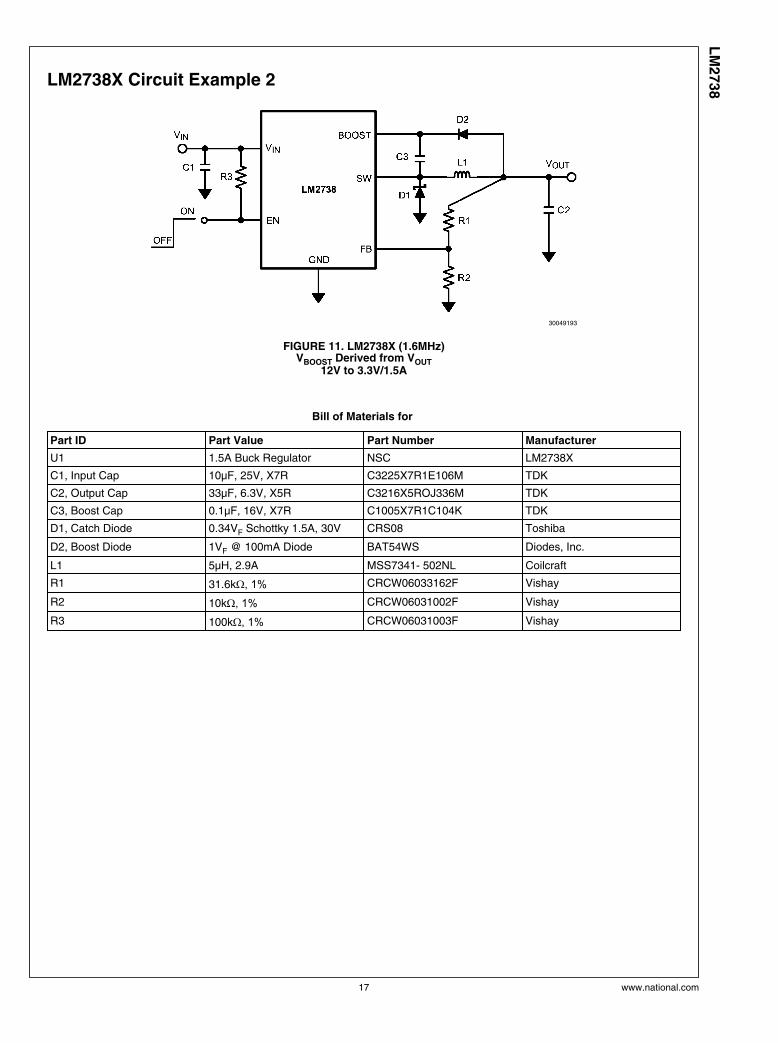
LM2738X Circuit Example 2
30049193
FIGURE 11. LM2738X (1.6MHz)VBOOST Derived from VOUT
12V to 3.3V/1.5A
Bill of Materials for
Part ID Part Value Part Number Manufacturer
U1 1.5A Buck Regulator NSC LM2738X
C1, Input Cap 10µF, 25V, X7R C3225X7R1E106M TDK
C2, Output Cap 33µF, 6.3V, X5R C3216X5ROJ336M TDK
C3, Boost Cap 0.1µF, 16V, X7R C1005X7R1C104K TDK
D1, Catch Diode 0.34VF Schottky 1.5A, 30V CRS08 Toshiba
D2, Boost Diode 1VF @ 100mA Diode BAT54WS Diodes, Inc.
L1 5µH, 2.9A MSS7341- 502NL Coilcraft
R1 31.6kΩ, 1% CRCW06033162F Vishay
R2 10kΩ, 1% CRCW06031002F Vishay
R3 100kΩ, 1% CRCW06031003F Vishay
17 www.national.com
LM
2738

LM2738X Circuit Example 3
30049144
FIGURE 12. LM2738X (1.6MHz)VBOOST Derived from VSHUNT
18V to 1.5V/1.5A
Bill of Materials for
Part ID Part Value Part Number Manufacturer
U1 1.5A Buck Regulator LM2738X National Semiconductor
C1, Input Cap 10µF, 25V, X7R C3225X7R1E106M TDK
C2, Output Cap 47µF, 6.3V, X5R C3216X5ROJ476M TDK
C3, Boost Cap 0.1µF, 16V, X7R C1005X7R1C104K TDK
C4, Shunt Cap 0.1µF, 6.3V, X5R C1005X5R0J104K TDK
D1, Catch Diode 0.34VF Schottky 1.5A, 30V CRS08 Toshiba
D2, Boost Diode 1VF @ 100mA Diode BAT54WS Diodes, Inc.
D3, Zener Diode 5.1V 250Mw SOT-23 BZX84C5V1 Vishay
L1 2.7µH, 1.76A VLCF5020T-2R7N1R7 TDK
R1 8.87kΩ, 1% CRCW06038871F Vishay
R2 10.2kΩ, 1% CRCW06031022F Vishay
R3 100kΩ, 1% CRCW06031003F Vishay
R4 4.12kΩ, 1% CRCW06034121F Vishay
www.national.com 18
LM
2738

LM2738X Circuit Example 4
30049149
FIGURE 13. LM2738X (1.6MHz)VBOOST Derived from Series Zener Diode (VIN)
15V to 1.5V/1.5A
Bill of Materials for
Part ID Part Value Part Number Manufacturer
U1 1.5A Buck Regulator LM2738X National Semiconductor
C1, Input Cap 10µF, 25V, X7R C3225X7R1E106M TDK
C2, Output Cap 47µF, 6.3V, X5R C3216X5ROJ476M TDK
C3, Boost Cap 0.1µF, 16V, X7R C1005X7R1C104K TDK
D1, Catch Diode 0.34VF Schottky 1.5A, 30V CRS08 Toshiba
D2, Boost Diode 1VF @ 100mA Diode BAT54WS Diodes, Inc.
D3, Zener Diode 11V 350Mw SOT-23 BZX84C11T Diodes, Inc.
L1 3.3µH, 3.5A MSS7341-332NL Coilcraft
R1 8.87kΩ, 1% CRCW06038871F Vishay
R2 10.2kΩ, 1% CRCW06031022F Vishay
R3 100kΩ, 1% CRCW06031003F Vishay
19 www.national.com
LM
2738

LM2738X Circuit Example 5
30049150
FIGURE 14. LM2738X (1.6MHz)VBOOST Derived from Series Zener Diode (VOUT)
15V to 9V/1.5A
Bill of Materials for
Part ID Part Value Part Number Manufacturer
U1 1.5A Buck Regulator LM2738X National Semiconductor
C1, Input Cap 10µF, 25V, X7R C3225X7R1E106M TDK
C2, Output Cap 22µF, 16V, X5R C3216X5R1C226M TDK
C3, Boost Cap 0.1µF, 16V, X7R C1005X7R1C104K TDK
D1, Catch Diode 0.34VF Schottky 1.5A, 30V CRS08 Toshiba
D2, Boost Diode 1VF @ 100mA Diode BAT54WS Diodes, Inc.
D3, Zener Diode 4.3V 350mw SOT-23 BZX84C4V3 Diodes, Inc.
L1 6.2µH, 2.5A MSS7341-622NL Coilcraft
R1 102kΩ, 1% CRCW06031023F Vishay
R2 10.2kΩ, 1% CRCW06031022F Vishay
R3 100kΩ, 1% CRCW06031003F Vishay
www.national.com 20
LM
2738

LM2738Y Circuit Example 6
30049142
FIGURE 15. LM2738Y (550kHz)VBOOST Derived from VIN
5V to 1.5V/1.5A
Bill of Materials for Figure 15
Part ID Part Value Part Number Manufacturer
U1 1.5A Buck Regulator LM2738Y National Semiconductor
C1, Input Cap 10µF, 6.3V, X5R C3216X5ROJ106M TDK
C2, Output Cap 47µF, 6.3V, X5R C3216X5ROJ476M TDK
C3, Boost Cap 0.1µF, 16V, X7R C1005X7R1C104K TDK
D1, Catch Diode 0.34VF Schottky 1.5A, 30V CRS08 Toshiba
D2, Boost Diode 1VF @ 100mA Diode BAT54WS Diodes, Inc.
L1 6.2µH, 2.5A, MSS7341-622NL Coilcraft
R1 8.87kΩ, 1% CRCW06038871F Vishay
R2 10.2kΩ, 1% CRCW06031022F Vishay
R3 100kΩ, 1% CRCW06031003F Vishay
21 www.national.com
LM
2738

LM2738Y Circuit Example 7
30049193
FIGURE 16. LM2738Y (550kHz)VBOOST Derived from VOUT
12V to 3.3V/1.5A
Bill of Materials for
Part ID Part Value Part Number Manufacturer
U1 1.5A Buck Regulator LM2738Y National Semiconductor
C1, Input Cap 10µF, 25V, X7R C3225X7R1E106M TDK
C2, Output Cap 47µF, 6.3V, X5R C3216X5ROJ476M TDK
C3, Boost Cap 0.1µF, 16V, X7R C1005X7R1C104K TDK
D1, Catch Diode 0.34VF Schottky 1.5A, 30V CRS08 Toshiba
D2, Boost Diode 1VF @ 100mA Diode BAT54WS Vishay
L1 12µH, 1.7A, MSS7341-123NL Coilcraft
R1 31.6kΩ, 1% CRCW06033162F Vishay
R2 10.0 kΩ, 1% CRCW06031002F Vishay
R3 100kΩ, 1% CRCW06031003F Vishay
www.national.com 22
LM
2738
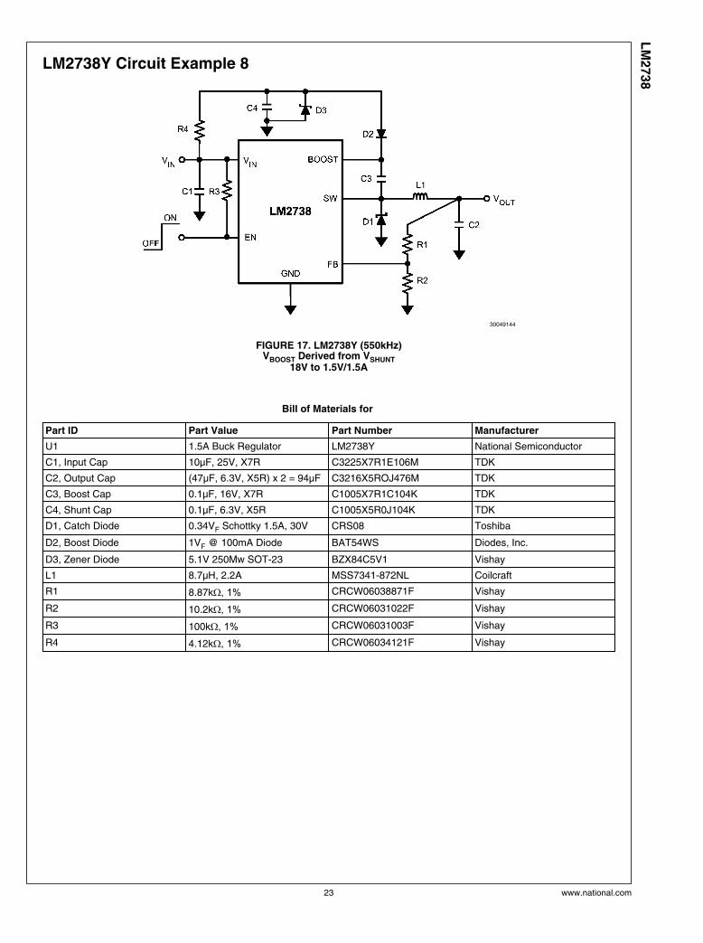
LM2738Y Circuit Example 8
30049144
FIGURE 17. LM2738Y (550kHz)VBOOST Derived from VSHUNT
18V to 1.5V/1.5A
Bill of Materials for
Part ID Part Value Part Number Manufacturer
U1 1.5A Buck Regulator LM2738Y National Semiconductor
C1, Input Cap 10µF, 25V, X7R C3225X7R1E106M TDK
C2, Output Cap (47µF, 6.3V, X5R) x 2 = 94µF C3216X5ROJ476M TDK
C3, Boost Cap 0.1µF, 16V, X7R C1005X7R1C104K TDK
C4, Shunt Cap 0.1µF, 6.3V, X5R C1005X5R0J104K TDK
D1, Catch Diode 0.34VF Schottky 1.5A, 30V CRS08 Toshiba
D2, Boost Diode 1VF @ 100mA Diode BAT54WS Diodes, Inc.
D3, Zener Diode 5.1V 250Mw SOT-23 BZX84C5V1 Vishay
L1 8.7µH, 2.2A MSS7341-872NL Coilcraft
R1 8.87kΩ, 1% CRCW06038871F Vishay
R2 10.2kΩ, 1% CRCW06031022F Vishay
R3 100kΩ, 1% CRCW06031003F Vishay
R4 4.12kΩ, 1% CRCW06034121F Vishay
23 www.national.com
LM
2738

LM2738Y Circuit Example 9
30049149
FIGURE 18. LM2738Y (550kHz)VBOOST Derived from Series Zener Diode (VIN)
15V to 1.5V/1.5A
Bill of Materials for
Part ID Part Value Part Number Manufacturer
U1 1.5A Buck Regulator LM2738Y National Semiconductor
C1, Input Cap 10µF, 25V, X7R C3225X7R1E106M TDK
C2, Output Cap (47µF, 6.3V, X5R) x 2 = 94µF C3216X5ROJ476M TDK
C3, Boost Cap 0.1µF, 16V, X7R C1005X7R1C104K TDK
D1, Catch Diode 0.34VF Schottky 1.5A, 30V CRS08 Toshiba
D2, Boost Diode 1VF @ 100mA Diode BAT54WS Diodes, Inc.
D3, Zener Diode 11V 350Mw SOT-23 BZX84C11T Diodes, Inc.
L1 8.7µH, 2.2A MSS7341-872NL Coilcraft
R1 8.87kΩ, 1% CRCW06038871F Vishay
R2 10.2kΩ, 1% CRCW06031022F Vishay
R3 100kΩ, 1% CRCW06031003F Vishay
www.national.com 24
LM
2738

LM2738Y Circuit Example 10
30049150
FIGURE 19. LM2738Y (550kHz)VBOOST Derived from Series Zener Diode (VOUT)
15V to 9V/1.5A
Bill of Materials for
Part ID Part Value Part Number Manufacturer
U1 1.5A Buck Regulator LM2738Y National Semiconductor
C1, Input Cap 10µF, 25V, X7R C3225X7R1E106M TDK
C2, Output Cap 22µF, 16V, X5R C3216X5R1C226M TDK
C3, Boost Cap 0.1µF, 16V, X7R C1005X7R1C104K TDK
D1, Catch Diode 0.34VF Schottky 1.5A, 30V CRS08 Toshiba
D2, Boost Diode 1VF @ 100mA Diode BAT54WS Diodes, Inc.
D3, Zener Diode 4.3V 350mw SOT-23 BZX84C4V3 Diodes, Inc.
L1 15µH, 2.1A SLF7055T150M2R1-3PF TDK
R1 102kΩ, 1% CRCW06031023F Vishay
R2 10.2kΩ, 1% CRCW06031022F Vishay
R3 100kΩ, 1% CRCW06031003F Vishay
25 www.national.com
LM
2738

Physical Dimensions inches (millimeters) unless otherwise noted
8-Lead LLP PackageNS Package Number SDA08A
8-Lead eMSOP PackageNS Package Number MUY08A
www.national.com 26
LM
2738

Notes
27 www.national.com
LM
2738
NotesL
M2738 5
50kH
z/1.6
MH
z 1.5
A S
tep
-Do
wn
DC
-DC
Sw
itch
ing
Reg
ula
tor
For more National Semiconductor product information and proven design tools, visit the following Web sites at:
Products Design Support
Amplifiers www.national.com/amplifiers WEBENCH www.national.com/webench
Audio www.national.com/audio Analog University www.national.com/AU
Clock Conditioners www.national.com/timing App Notes www.national.com/appnotes
Data Converters www.national.com/adc Distributors www.national.com/contacts
Displays www.national.com/displays Green Compliance www.national.com/quality/green
Ethernet www.national.com/ethernet Packaging www.national.com/packaging
Interface www.national.com/interface Quality and Reliability www.national.com/quality
LVDS www.national.com/lvds Reference Designs www.national.com/refdesigns
Power Management www.national.com/power Feedback www.national.com/feedback
Switching Regulators www.national.com/switchers
LDOs www.national.com/ldo
LED Lighting www.national.com/led
PowerWise www.national.com/powerwise
Serial Digital Interface (SDI) www.national.com/sdi
Temperature Sensors www.national.com/tempsensors
Wireless (PLL/VCO) www.national.com/wireless
THE CONTENTS OF THIS DOCUMENT ARE PROVIDED IN CONNECTION WITH NATIONAL SEMICONDUCTOR CORPORATION(“NATIONAL”) PRODUCTS. NATIONAL MAKES NO REPRESENTATIONS OR WARRANTIES WITH RESPECT TO THE ACCURACYOR COMPLETENESS OF THE CONTENTS OF THIS PUBLICATION AND RESERVES THE RIGHT TO MAKE CHANGES TOSPECIFICATIONS AND PRODUCT DESCRIPTIONS AT ANY TIME WITHOUT NOTICE. NO LICENSE, WHETHER EXPRESS,IMPLIED, ARISING BY ESTOPPEL OR OTHERWISE, TO ANY INTELLECTUAL PROPERTY RIGHTS IS GRANTED BY THISDOCUMENT.
TESTING AND OTHER QUALITY CONTROLS ARE USED TO THE EXTENT NATIONAL DEEMS NECESSARY TO SUPPORTNATIONAL’S PRODUCT WARRANTY. EXCEPT WHERE MANDATED BY GOVERNMENT REQUIREMENTS, TESTING OF ALLPARAMETERS OF EACH PRODUCT IS NOT NECESSARILY PERFORMED. NATIONAL ASSUMES NO LIABILITY FORAPPLICATIONS ASSISTANCE OR BUYER PRODUCT DESIGN. BUYERS ARE RESPONSIBLE FOR THEIR PRODUCTS ANDAPPLICATIONS USING NATIONAL COMPONENTS. PRIOR TO USING OR DISTRIBUTING ANY PRODUCTS THAT INCLUDENATIONAL COMPONENTS, BUYERS SHOULD PROVIDE ADEQUATE DESIGN, TESTING AND OPERATING SAFEGUARDS.
EXCEPT AS PROVIDED IN NATIONAL’S TERMS AND CONDITIONS OF SALE FOR SUCH PRODUCTS, NATIONAL ASSUMES NOLIABILITY WHATSOEVER, AND NATIONAL DISCLAIMS ANY EXPRESS OR IMPLIED WARRANTY RELATING TO THE SALEAND/OR USE OF NATIONAL PRODUCTS INCLUDING LIABILITY OR WARRANTIES RELATING TO FITNESS FOR A PARTICULARPURPOSE, MERCHANTABILITY, OR INFRINGEMENT OF ANY PATENT, COPYRIGHT OR OTHER INTELLECTUAL PROPERTYRIGHT.
LIFE SUPPORT POLICY
NATIONAL’S PRODUCTS ARE NOT AUTHORIZED FOR USE AS CRITICAL COMPONENTS IN LIFE SUPPORT DEVICES ORSYSTEMS WITHOUT THE EXPRESS PRIOR WRITTEN APPROVAL OF THE CHIEF EXECUTIVE OFFICER AND GENERALCOUNSEL OF NATIONAL SEMICONDUCTOR CORPORATION. As used herein:
Life support devices or systems are devices which (a) are intended for surgical implant into the body, or (b) support or sustain life andwhose failure to perform when properly used in accordance with instructions for use provided in the labeling can be reasonably expectedto result in a significant injury to the user. A critical component is any component in a life support device or system whose failure to performcan be reasonably expected to cause the failure of the life support device or system or to affect its safety or effectiveness.
National Semiconductor and the National Semiconductor logo are registered trademarks of National Semiconductor Corporation. All otherbrand or product names may be trademarks or registered trademarks of their respective holders.
Copyright© 2008 National Semiconductor Corporation
For the most current product information visit us at www.national.com
National SemiconductorAmericas TechnicalSupport CenterEmail:[email protected]: 1-800-272-9959
National Semiconductor EuropeTechnical Support CenterEmail: [email protected] Tel: +49 (0) 180 5010 771English Tel: +44 (0) 870 850 4288
National Semiconductor AsiaPacific Technical Support CenterEmail: [email protected]
National Semiconductor JapanTechnical Support CenterEmail: [email protected]
www.national.com


![MITSUBISHI ELECTRIC Global website...1.5A/ 6.5 [Power Supply] R61P [CPU] R04CPU RY40NT5P Total Consumption Current 1.5A / 6.5A S V DC 32 / current consumption 1.5A /s_SA /6.5A Az áramfelvétel](https://static.fdocuments.in/doc/165x107/5f36fe787071e7134c12f678/mitsubishi-electric-global-website-15a-65-power-supply-r61p-cpu-r04cpu.jpg)