LM1875 20W Audio Power Amplifier (Rev. A)LM1875 20W Audio Power Amplifier Check for Samples: LM1875...
14
LM1875 www.ti.com SNAS524A – MAY 2004 – REVISED MAY 2004 LM1875 20W Audio Power Amplifier Check for Samples: LM1875 1FEATURES DESCRIPTION The LM1875 is a monolithic power amplifier offering 2• Up to 30 Watts Output Power very low distortion and high quality performance for • A VO Typically 90 dB consumer audio applications. • Low Distortion: 0.015%, 1 kHz, 20 W The LM1875 delivers 20 watts into a 4Ω or 8Ω load • Wide Power Bandwidth: 70 kHz on ±25V supplies. Using an 8Ω load and ±30V • Protection for AC and DC Short Circuits to supplies, over 30 watts of power may be delivered. The amplifier is designed to operate with a minimum Ground of external components. Device overload protection • Thermal Protection with Parole Circuit consists of both internal current limit and thermal • High Current Capability: 4A shutdown. • Wide Supply Range 16V-60V The LM1875 design takes advantage of advanced • Internal Output Protection Diodes circuit techniques and processing to achieve extremely low distortion levels even at high output • 94 dB Ripple Rejection power levels. Other outstanding features include high • Plastic Power Package TO-220 gain, fast slew rate and a wide power bandwidth, large output voltage swing, high current capability, APPLICATIONS and a very wide supply range. The amplifier is • High Performance Audio Systems internally compensated and stable for gains of 10 or greater. • Bridge Amplifiers • Stereo Phonographs • Servo Amplifiers • Instrument Systems Connection Diagram Figure 1. NDH0005D, KC0005A, NEB0005E, NEB0005B, Front View 1 Please be aware that an important notice concerning availability, standard warranty, and use in critical applications of Texas Instruments semiconductor products and disclaimers thereto appears at the end of this data sheet. 2All trademarks are the property of their respective owners. PRODUCTION DATA information is current as of publication date. Copyright © 2004, Texas Instruments Incorporated Products conform to specifications per the terms of the Texas Instruments standard warranty. Production processing does not necessarily include testing of all parameters.
Transcript of LM1875 20W Audio Power Amplifier (Rev. A)LM1875 20W Audio Power Amplifier Check for Samples: LM1875...

LM1875
www.ti.com SNAS524A –MAY 2004–REVISED MAY 2004
LM1875 20W Audio Power AmplifierCheck for Samples: LM1875
1FEATURES DESCRIPTIONThe LM1875 is a monolithic power amplifier offering
2• Up to 30 Watts Output Powervery low distortion and high quality performance for
• AVO Typically 90 dB consumer audio applications.• Low Distortion: 0.015%, 1 kHz, 20 W
The LM1875 delivers 20 watts into a 4Ω or 8Ω load• Wide Power Bandwidth: 70 kHz on ±25V supplies. Using an 8Ω load and ±30V• Protection for AC and DC Short Circuits to supplies, over 30 watts of power may be delivered.
The amplifier is designed to operate with a minimumGroundof external components. Device overload protection• Thermal Protection with Parole Circuitconsists of both internal current limit and thermal
• High Current Capability: 4A shutdown.• Wide Supply Range 16V-60V
The LM1875 design takes advantage of advanced• Internal Output Protection Diodes circuit techniques and processing to achieve
extremely low distortion levels even at high output• 94 dB Ripple Rejectionpower levels. Other outstanding features include high• Plastic Power Package TO-220gain, fast slew rate and a wide power bandwidth,large output voltage swing, high current capability,APPLICATIONS and a very wide supply range. The amplifier is
• High Performance Audio Systems internally compensated and stable for gains of 10 orgreater.• Bridge Amplifiers
• Stereo Phonographs• Servo Amplifiers• Instrument Systems
Connection Diagram
Figure 1. NDH0005D, KC0005A,NEB0005E, NEB0005B,
Front View
1
Please be aware that an important notice concerning availability, standard warranty, and use in critical applications ofTexas Instruments semiconductor products and disclaimers thereto appears at the end of this data sheet.
2All trademarks are the property of their respective owners.
PRODUCTION DATA information is current as of publication date. Copyright © 2004, Texas Instruments IncorporatedProducts conform to specifications per the terms of the TexasInstruments standard warranty. Production processing does notnecessarily include testing of all parameters.
LM1875
SNAS524A –MAY 2004–REVISED MAY 2004 www.ti.com
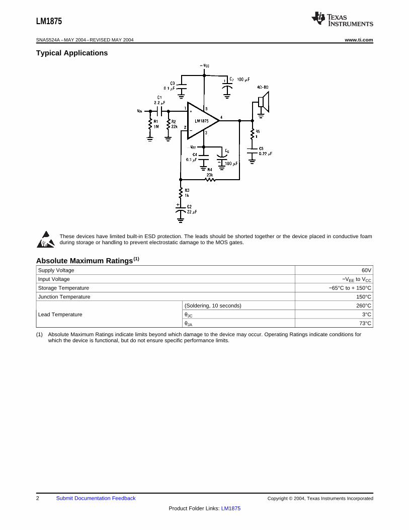
Typical Applications
These devices have limited built-in ESD protection. The leads should be shorted together or the device placed in conductive foamduring storage or handling to prevent electrostatic damage to the MOS gates.
Absolute Maximum Ratings (1)
Supply Voltage 60V
Input Voltage −VEE to VCC
Storage Temperature −65°C to + 150°C
Junction Temperature 150°C
(Soldering, 10 seconds) 260°C
Lead Temperature θJC 3°C
θJA 73°C
(1) Absolute Maximum Ratings indicate limits beyond which damage to the device may occur. Operating Ratings indicate conditions forwhich the device is functional, but do not ensure specific performance limits.
2 Submit Documentation Feedback Copyright © 2004, Texas Instruments Incorporated
Product Folder Links: LM1875

LM1875
www.ti.com SNAS524A –MAY 2004–REVISED MAY 2004
Electrical CharacteristicsVCC=+25V, −VEE=−25V, TAMBIENT=25°C, RL=8Ω, AV=20 (26 dB), fo=1 kHz, unless otherwise specified.
Parameter Conditions Typical Tested Limits Units
Supply Current POUT=0W 70 100 mA
Output Power (1) THD=1% 25 W
THD (1) POUT=20W, fo=1 kHz 0.015 %
POUT=20W, fo=20 kHz 0.05 0.4 %
POUT=20W, RL=4Ω, fo=1 kHz 0.022 %
POUT=20W, RL=4Ω, fo=20 kHz 0.07 0.6 %
Offset Voltage ±1 ±15 mV
Input Bias Current ±0.2 ±2 μA
Input Offset Current 0 ±0.5 μA
Gain-Bandwidth Product fo=20 kHz 5.5 MHz
Open Loop Gain DC 90 dB
PSRR VCC, 1 kHz, 1 Vrms 95 52 dB
VEE, 1 kHz, 1 Vrms 83 52 dB
Max Slew Rate 20W, 8Ω, 70 kHz BW 8 V/μs
Current Limit VOUT = VSUPPLY −10V 4 3 A
Equivalent Input Noise Voltage RS=600Ω, CCIR 3 μVrms
(1) Assumes the use of a heat sink having a thermal resistance of 1°C/W and no insulator with an ambient temperature of 25°C. Becausethe output limiting circuitry has a negative temperature coefficient, the maximum output power delivered to a 4Ω load may be slightlyreduced when the tab temperature exceeds 55°C.
Typical Applications For Single Supply Operation
Figure 2.
Copyright © 2004, Texas Instruments Incorporated Submit Documentation Feedback 3
Product Folder Links: LM1875

LM1875
SNAS524A –MAY 2004–REVISED MAY 2004 www.ti.com
Typical Performance Characteristics
THD vs Power Output THD vs Frequency
Figure 3. Figure 4.
Power Output vs Supply Supply Current vs SupplyVoltage Voltage
Figure 5. Figure 6.
PSRR vs Frequency Device Dissipation vs Ambient Temperature†
†φINTERFACE = 1°C/W.See Application Hints.
Figure 7. Figure 8.
4 Submit Documentation Feedback Copyright © 2004, Texas Instruments Incorporated
Product Folder Links: LM1875

LM1875
www.ti.com SNAS524A –MAY 2004–REVISED MAY 2004
Typical Performance Characteristics (continued)Power Dissipation vs Power Output Power Dissipation vs Power Output
Figure 9. Figure 10.
IOUT vs VOUT-Current Limit/Safe Operating Area Boundary Open Loop Gain and Phase vs Frequency
Thermal shutdown with infinite heat sinkThermal shutdown with 1°C/W heat sink
Figure 11. Figure 12.
Input Bias Current vs Supply Voltage
Figure 13.
Copyright © 2004, Texas Instruments Incorporated Submit Documentation Feedback 5
Product Folder Links: LM1875

LM1875
SNAS524A –MAY 2004–REVISED MAY 2004 www.ti.com
Schematic Diagram
6 Submit Documentation Feedback Copyright © 2004, Texas Instruments Incorporated
Product Folder Links: LM1875

LM1875
www.ti.com SNAS524A –MAY 2004–REVISED MAY 2004
APPLICATION HINTS
STABILITY
The LM1875 is designed to be stable when operated at a closed-loop gain of 10 or greater, but, as with anyother high-current amplifier, the LM1875 can be made to oscillate under certain conditions. These usually involveprinted circuit board layout or output/input coupling.
Proper layout of the printed circuit board is very important. While the LM1875 will be stable when installed in aboard similar to the ones shown in this data sheet, it is sometimes necessary to modify the layout somewhat tosuit the physical requirements of a particular application. When designing a different layout, it is important toreturn the load ground, the output compensation ground, and the low level (feedback and input) grounds to thecircuit board ground point through separate paths. Otherwise, large currents flowing along a ground conductorwill generate voltages on the conductor which can effectively act as signals at the input, resulting in highfrequency oscillation or excessive distortion. It is advisable to keep the output compensation components and the0.1 μF supply decoupling capacitors as close as possible to the LM1875 to reduce the effects of PCB traceresistance and inductance. For the same reason, the ground return paths for these components should be asshort as possible.
Occasionally, current in the output leads (which function as antennas) can be coupled through the air to theamplifier input, resulting in high-frequency oscillation. This normally happens when the source impedance is highor the input leads are long. The problem can be eliminated by placing a small capacitor (on the order of 50 pF to500 pF) across the circuit input.
Most power amplifiers do not drive highly capacitive loads well, and the LM1875 is no exception. If the output ofthe LM1875 is connected directly to a capacitor with no series resistance, the square wave response will exhibitringing if the capacitance is greater than about 0.1 μF. The amplifier can typically drive load capacitances up to 2μF or so without oscillating, but this is not recommended. If highly capacitive loads are expected, a resistor (atleast 1Ω) should be placed in series with the output of the LM1875. A method commonly employed to protectamplifiers from low impedances at high frequencies is to couple to the load through a 10Ω resistor in parallel witha 5 μH inductor.
DISTORTION
The preceding suggestions regarding circuit board grounding techniques will also help to prevent excessivedistortion levels in audio applications. For low THD, it is also necessary to keep the power supply traces andwires separated from the traces and wires connected to the inputs of the LM1875. This prevents the powersupply currents, which are large and nonlinear, from inductively coupling to the LM1875 inputs. Power supplywires should be twisted together and separated from the circuit board. Where these wires are soldered to theboard, they should be perpendicular to the plane of the board at least to a distance of a couple of inches. With aproper physical layout, THD levels at 20 kHz with 10W output to an 8Ω load should be less than 0.05%, and lessthan 0.02% at 1 kHz.
CURRENT LIMIT AND SAFE OPERATING AREA (SOA) PROTECTION
A power amplifier's output transistors can be damaged by excessive applied voltage, current flow, or powerdissipation. The voltage applied to the amplifier is limited by the design of the external power supply, while themaximum current passed by the output devices is usually limited by internal circuitry to some fixed value. Short-term power dissipation is usually not limited in monolithic audio power amplifiers, and this can be a problemwhen driving reactive loads, which may draw large currents while high voltages appear on the output transistors.The LM1875 not only limits current to around 4A, but also reduces the value of the limit current when an outputtransistor has a high voltage across it.
When driving nonlinear reactive loads such as motors or loudspeakers with built-in protection relays, there is apossibility that an amplifier output will be connected to a load whose terminal voltage may attempt to swingbeyond the power supply voltages applied to the amplifier. This can cause degradation of the output transistorsor catastrophic failure of the whole circuit. The standard protection for this type of failure mechanism is a pair ofdiodes connected between the output of the amplifier and the supply rails. These are part of the internal circuitryof the LM1875, and needn't be added externally when standard reactive loads are driven.
Copyright © 2004, Texas Instruments Incorporated Submit Documentation Feedback 7
Product Folder Links: LM1875

LM1875
SNAS524A –MAY 2004–REVISED MAY 2004 www.ti.com
THERMAL PROTECTION
The LM1875 has a sophisticated thermal protection scheme to prevent long-term thermal stress to the device.When the temperature on the die reaches 170°C, the LM1875 shuts down. It starts operating again when the dietemperature drops to about 145°C, but if the temperature again begins to rise, shutdown will occur at only 150°C.Therefore, the device is allowed to heat up to a relatively high temperature if the fault condition is temporary, buta sustained fault will limit the maximum die temperature to a lower value. This greatly reduces the stressesimposed on the IC by thermal cycling, which in turn improves its reliability under sustained fault conditions.
Since the die temperature is directly dependent upon the heat sink, the heat sink should be chosen for thermalresistance low enough that thermal shutdown will not be reached during normal operation. Using the best heatsink possible within the cost and space constraints of the system will improve the long-term reliability of anypower semiconductor device.
POWER DISSIPATION AND HEAT SINKING
The LM1875 must always be operated with a heat sink, even when it is not required to drive a load. Themaximum idling current of the device is 100 mA, so that on a 60V power supply an unloaded LM1875 mustdissipate 6W of power. The 54°C/W junction-to-ambient thermal resistance of a TO-220 package would causethe die temperature to rise 324°C above ambient, so the thermal protection circuitry will shut the amplifier down ifoperation without a heat sink is attempted.
In order to determine the appropriate heat sink for a given application, the power dissipation of the LM1875 inthat application must be known. When the load is resistive, the maximum average power that the IC will berequired to dissipate is approximately:
where• VS is the total power supply voltage across the LM1875• RL is the load resistance• PQ is the quiescent power dissipation of the amplifier
The above equation is only an approximation which assumes an “ideal” class B output stage and constant powerdissipation in all other parts of the circuit. The curves of “Power Dissipation vs Power Output” give a betterrepresentation of the behavior of the LM1875 with various power supply voltages and resistive loads. As anexample, if the LM1875 is operated on a 50V power supply with a resistive load of 8Ω, it can develop up to 19Wof internal power dissipation. If the die temperature is to remain below 150°C for ambient temperatures up to70°C, the total junction-to-ambient thermal resistance must be less than
Using θJC=2°C/W, the sum of the case-to-heat-sink interface thermal resistance and the heat-sink-to-ambientthermal resistance must be less than 2.2°C/W. The case-to-heat-sink thermal resistance of the TO-220 packagevaries with the mounting method used. A metal-to-metal interface will be about 1°C/W if lubricated, and about1.2°C/W if dry.
If a mica insulator is used, the thermal resistance will be about 1.6°C/W lubricated and 3.4°C/W dry. For thisexample, we assume a lubricated mica insulator between the LM1875 and the heat sink. The heat sink thermalresistance must then be less than4.2°C/W−2°C/W−1.6°C/W=0.6°C/W.
This is a rather large heat sink and may not be practical in some applications. If a smaller heat sink is requiredfor reasons of size or cost, there are two alternatives. [EM00001]The maximum ambient operating temperaturecan be reduced to 50°C (122°F), resulting in a 1.6°C/W heat sink, or the heat sink can be isolated from thechassis so the mica washer is not needed. This will change the required heat sink to a 1.2°C/W unit if the case-to-heat-sink interface is lubricated.
8 Submit Documentation Feedback Copyright © 2004, Texas Instruments Incorporated
Product Folder Links: LM1875

LM1875
www.ti.com SNAS524A –MAY 2004–REVISED MAY 2004
NOTEWhen using a single supply, maximum transfer of heat away from the LM1875 can beachieved by mounting the device directly to the heat sink (tab is at ground potential); thisavoids the use of a mica or other type insulator.
The thermal requirements can become more difficult when an amplifier is driving a reactive load. For a givenmagnitude of load impedance, a higher degree of reactance will cause a higher level of power dissipation withinthe amplifier. As a general rule, the power dissipation of an amplifier driving a 60° reactive load (usuallyconsidered to be a worst-case loudspeaker load) will be roughly that of the same amplifier driving the resistivepart of that load. For example, a loudspeaker may at some frequency have an impedance with a magnitude of8Ω and a phase angle of 60°. The real part of this load will then be 4Ω, and the amplifier power dissipation willroughly follow the curve of power dissipation with a 4Ω load.
Component Layouts
Figure 14. Split Supply
Copyright © 2004, Texas Instruments Incorporated Submit Documentation Feedback 9
Product Folder Links: LM1875

LM1875
SNAS524A –MAY 2004–REVISED MAY 2004 www.ti.com
Figure 15. Single Supply
10 Submit Documentation Feedback Copyright © 2004, Texas Instruments Incorporated
Product Folder Links: LM1875

PACKAGE OPTION ADDENDUM
www.ti.com 11-Apr-2013
Addendum-Page 1
PACKAGING INFORMATION
Orderable Device Status(1)
Package Type PackageDrawing
Pins PackageQty
Eco Plan(2)
Lead/Ball Finish MSL Peak Temp(3)
Op Temp (°C) Top-Side Markings(4)
Samples
LM1875T ACTIVE TO-220 NDH 5 45 TBD Call TI Call TI 0 to 70 LM1875T
LM1875T/LB02 ACTIVE TO-220 NEB 5 45 TBD Call TI Call TI LM1875T
LM1875T/LB03 ACTIVE TO-220 NDH 5 45 TBD Call TI Call TI LM1875T
LM1875T/LB05 ACTIVE TO-220 NEB 5 45 TBD Call TI Call TI LM1875T
LM1875T/LF02 ACTIVE TO-220 NEB 5 45 Green (RoHS& no Sb/Br)
CU SN Level-1-NA-UNLIM LM1875T
LM1875T/LF03 ACTIVE TO-220 NDH 5 45 Green (RoHS& no Sb/Br)
CU SN Level-1-NA-UNLIM LM1875T
LM1875T/LF05 ACTIVE TO-220 NEB 5 45 Green (RoHS& no Sb/Br)
CU SN Level-1-NA-UNLIM LM1875T
LM1875T/NOPB ACTIVE TO-220 NDH 5 45 Green (RoHS& no Sb/Br)
CU SN Level-1-NA-UNLIM 0 to 70 LM1875T
(1) The marketing status values are defined as follows:ACTIVE: Product device recommended for new designs.LIFEBUY: TI has announced that the device will be discontinued, and a lifetime-buy period is in effect.NRND: Not recommended for new designs. Device is in production to support existing customers, but TI does not recommend using this part in a new design.PREVIEW: Device has been announced but is not in production. Samples may or may not be available.OBSOLETE: TI has discontinued the production of the device.
(2) Eco Plan - The planned eco-friendly classification: Pb-Free (RoHS), Pb-Free (RoHS Exempt), or Green (RoHS & no Sb/Br) - please check http://www.ti.com/productcontent for the latest availabilityinformation and additional product content details.TBD: The Pb-Free/Green conversion plan has not been defined.Pb-Free (RoHS): TI's terms "Lead-Free" or "Pb-Free" mean semiconductor products that are compatible with the current RoHS requirements for all 6 substances, including the requirement thatlead not exceed 0.1% by weight in homogeneous materials. Where designed to be soldered at high temperatures, TI Pb-Free products are suitable for use in specified lead-free processes.Pb-Free (RoHS Exempt): This component has a RoHS exemption for either 1) lead-based flip-chip solder bumps used between the die and package, or 2) lead-based die adhesive used betweenthe die and leadframe. The component is otherwise considered Pb-Free (RoHS compatible) as defined above.Green (RoHS & no Sb/Br): TI defines "Green" to mean Pb-Free (RoHS compatible), and free of Bromine (Br) and Antimony (Sb) based flame retardants (Br or Sb do not exceed 0.1% by weightin homogeneous material)
(3) MSL, Peak Temp. -- The Moisture Sensitivity Level rating according to the JEDEC industry standard classifications, and peak solder temperature.
(4) Multiple Top-Side Markings will be inside parentheses. Only one Top-Side Marking contained in parentheses and separated by a "~" will appear on a device. If a line is indented then it is acontinuation of the previous line and the two combined represent the entire Top-Side Marking for that device.

MECHANICAL DATA
NDH0005D
www.ti.com

MECHANICAL DATA
NEB0005B
www.ti.com

MECHANICAL DATA
NEB0005E
www.ti.com