LM117/LM317A/LM317 3-Terminal Adjustable...
26
LM117/LM317A/LM317 3-Terminal Adjustable Regulator General Description The LM117 series of adjustable 3-terminal positive voltage regulators is capable of supplying in excess of 1.5A over a 1.2V to 37V output range. They are exceptionally easy to use and require only two external resistors to set the output voltage. Further, both line and load regulation are better than standard fixed regulators. Also, the LM117 is packaged in standard transistor packages which are easily mounted and handled. In addition to higher performance than fixed regulators, the LM117 series offers full overload protection available only in IC’s. Included on the chip are current limit, thermal overload protection and safe area protection. All overload protection circuitry remains fully functional even if the adjustment ter- minal is disconnected. Normally, no capacitors are needed unless the device is situated more than 6 inches from the input filter capacitors in which case an input bypass is needed. An optional output capacitor can be added to improve transient response. The adjustment terminal can be bypassed to achieve very high ripple rejection ratios which are difficult to achieve with stan- dard 3-terminal regulators. Besides replacing fixed regulators, the LM117 is useful in a wide variety of other applications. Since the regulator is “floating” and sees only the input-to-output differential volt- age, supplies of several hundred volts can be regulated as long as the maximum input to output differential is not ex- ceeded, i.e., avoid short-circuiting the output. Also, it makes an especially simple adjustable switching regulator, a programmable output regulator, or by connecting a fixed resistor between the adjustment pin and output, the LM117 can be used as a precision current regulator. Sup- plies with electronic shutdown can be achieved by clamping the adjustment terminal to ground which programs the out- put to 1.2V where most loads draw little current. For applications requiring greater output current, see LM150 series (3A) and LM138 series (5A) data sheets. For the negative complement, see LM137 series data sheet. Features n Guaranteed 1% output voltage tolerance (LM317A) n Guaranteed max. 0.01%/V line regulation (LM317A) n Guaranteed max. 0.3% load regulation (LM117) n Guaranteed 1.5A output current n Adjustable output down to 1.2V n Current limit constant with temperature n P + Product Enhancement tested n 80 dB ripple rejection n Output is short-circuit protected Typical Applications 1.2V–25V Adjustable Regulator 00906301 Full output current not available at high input-output voltages *Needed if device is more than 6 inches from filter capacitors. †Optional — improves transient response. Output capacitors in the range of 1μF to 1000μF of aluminum or tantalum electrolytic are commonly used to provide improved output impedance and rejection of transients. LM117/LM317A/LM317 Package Options Part Number Suffix Package Output Current LM117, LM317 K TO-3 1.5A LM317 T TO-220 1.5A LM317 S TO-263 1.5A LM317A, LM317 EMP SOT-223 1.0A LM117, LM317A, LM317 H TO-39 0.5A LM117 E LCC 0.5A LM317A, LM317 MDT TO-252 0.5A SOT-223 vs. TO-252 (D-Pak) Packages 00906354 Scale 1:1 June 2006 LM117/LM317A/LM317 3-Terminal Adjustable Regulator © 2006 National Semiconductor Corporation DS009063 www.national.com
Transcript of LM117/LM317A/LM317 3-Terminal Adjustable...
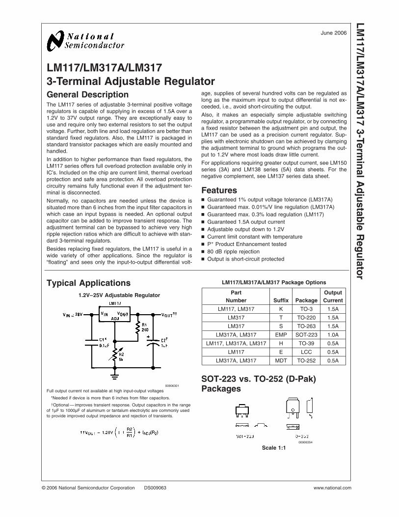
LM117/LM317A/LM3173-Terminal Adjustable RegulatorGeneral DescriptionThe LM117 series of adjustable 3-terminal positive voltageregulators is capable of supplying in excess of 1.5A over a1.2V to 37V output range. They are exceptionally easy touse and require only two external resistors to set the outputvoltage. Further, both line and load regulation are better thanstandard fixed regulators. Also, the LM117 is packaged instandard transistor packages which are easily mounted andhandled.
In addition to higher performance than fixed regulators, theLM117 series offers full overload protection available only inIC’s. Included on the chip are current limit, thermal overloadprotection and safe area protection. All overload protectioncircuitry remains fully functional even if the adjustment ter-minal is disconnected.
Normally, no capacitors are needed unless the device issituated more than 6 inches from the input filter capacitors inwhich case an input bypass is needed. An optional outputcapacitor can be added to improve transient response. Theadjustment terminal can be bypassed to achieve very highripple rejection ratios which are difficult to achieve with stan-dard 3-terminal regulators.
Besides replacing fixed regulators, the LM117 is useful in awide variety of other applications. Since the regulator is“floating” and sees only the input-to-output differential volt-
age, supplies of several hundred volts can be regulated aslong as the maximum input to output differential is not ex-ceeded, i.e., avoid short-circuiting the output.
Also, it makes an especially simple adjustable switchingregulator, a programmable output regulator, or by connectinga fixed resistor between the adjustment pin and output, theLM117 can be used as a precision current regulator. Sup-plies with electronic shutdown can be achieved by clampingthe adjustment terminal to ground which programs the out-put to 1.2V where most loads draw little current.
For applications requiring greater output current, see LM150series (3A) and LM138 series (5A) data sheets. For thenegative complement, see LM137 series data sheet.
Featuresn Guaranteed 1% output voltage tolerance (LM317A)n Guaranteed max. 0.01%/V line regulation (LM317A)n Guaranteed max. 0.3% load regulation (LM117)n Guaranteed 1.5A output currentn Adjustable output down to 1.2Vn Current limit constant with temperaturen P+ Product Enhancement testedn 80 dB ripple rejectionn Output is short-circuit protected
Typical Applications1.2V–25V Adjustable Regulator
00906301
Full output current not available at high input-output voltages
*Needed if device is more than 6 inches from filter capacitors.
†Optional — improves transient response. Output capacitors in the rangeof 1µF to 1000µF of aluminum or tantalum electrolytic are commonly usedto provide improved output impedance and rejection of transients.
LM117/LM317A/LM317 Package Options
PartNumber Suffix Package
OutputCurrent
LM117, LM317 K TO-3 1.5A
LM317 T TO-220 1.5A
LM317 S TO-263 1.5A
LM317A, LM317 EMP SOT-223 1.0A
LM117, LM317A, LM317 H TO-39 0.5A
LM117 E LCC 0.5A
LM317A, LM317 MDT TO-252 0.5A
SOT-223 vs. TO-252 (D-Pak)Packages
00906354
Scale 1:1
June 2006LM
117/LM317A
/LM317
3-TerminalA
djustableR
egulator
© 2006 National Semiconductor Corporation DS009063 www.national.com
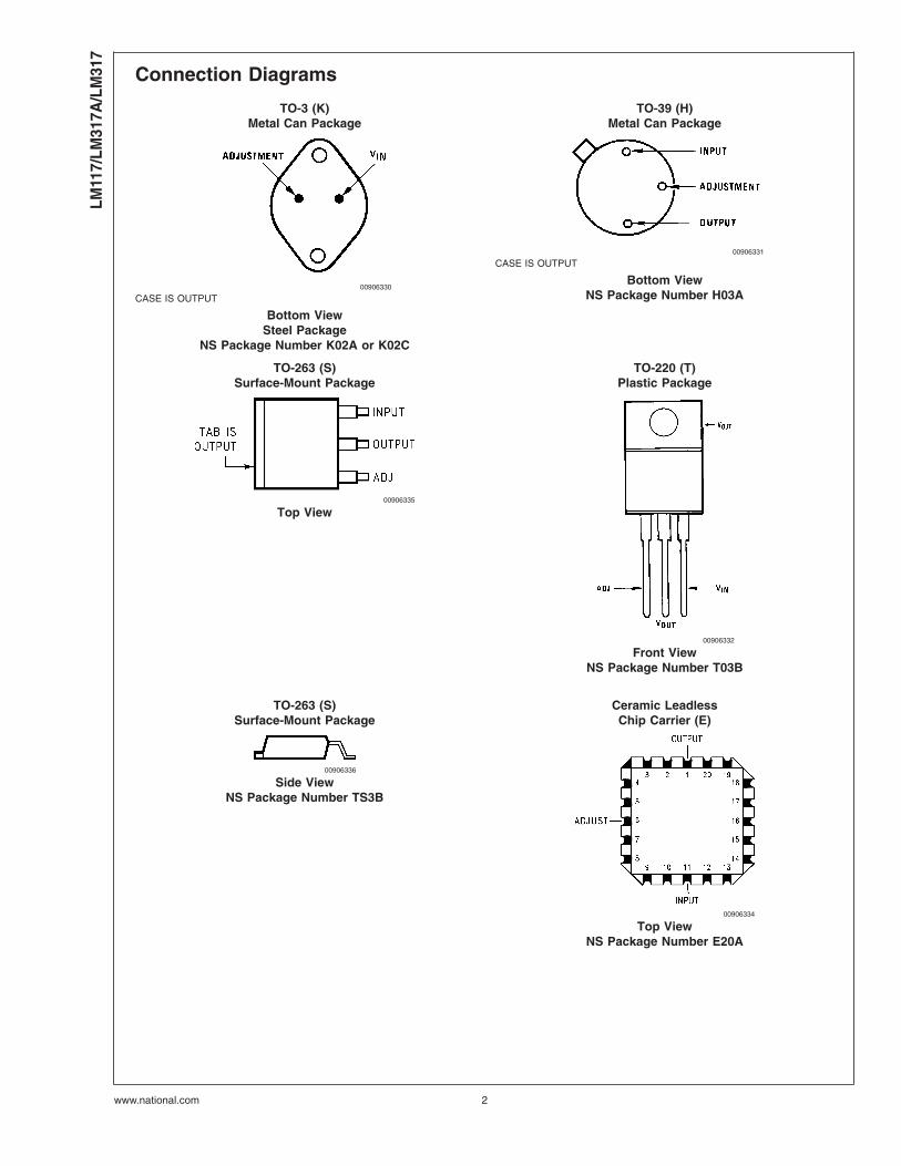
Connection Diagrams
TO-3 (K)Metal Can Package
TO-39 (H)Metal Can Package
00906330
CASE IS OUTPUT
Bottom ViewSteel Package
NS Package Number K02A or K02C
00906331
CASE IS OUTPUT
Bottom ViewNS Package Number H03A
TO-263 (S)Surface-Mount Package
TO-220 (T)Plastic Package
00906335
Top View
00906332
Front ViewNS Package Number T03B
TO-263 (S)Surface-Mount Package
Ceramic LeadlessChip Carrier (E)
00906336
Side ViewNS Package Number TS3B
00906334
Top ViewNS Package Number E20A
LM11
7/LM
317A
/LM
317
www.national.com 2
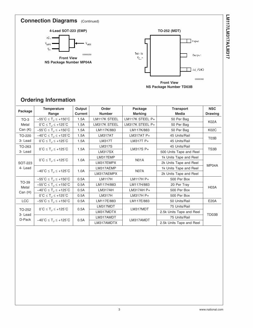
Connection Diagrams (Continued)
4-Lead SOT-223 (EMP) TO-252 (MDT)
00906359
Front ViewNS Package Number MP04A
00906366
Front ViewNS Package Number TD03B
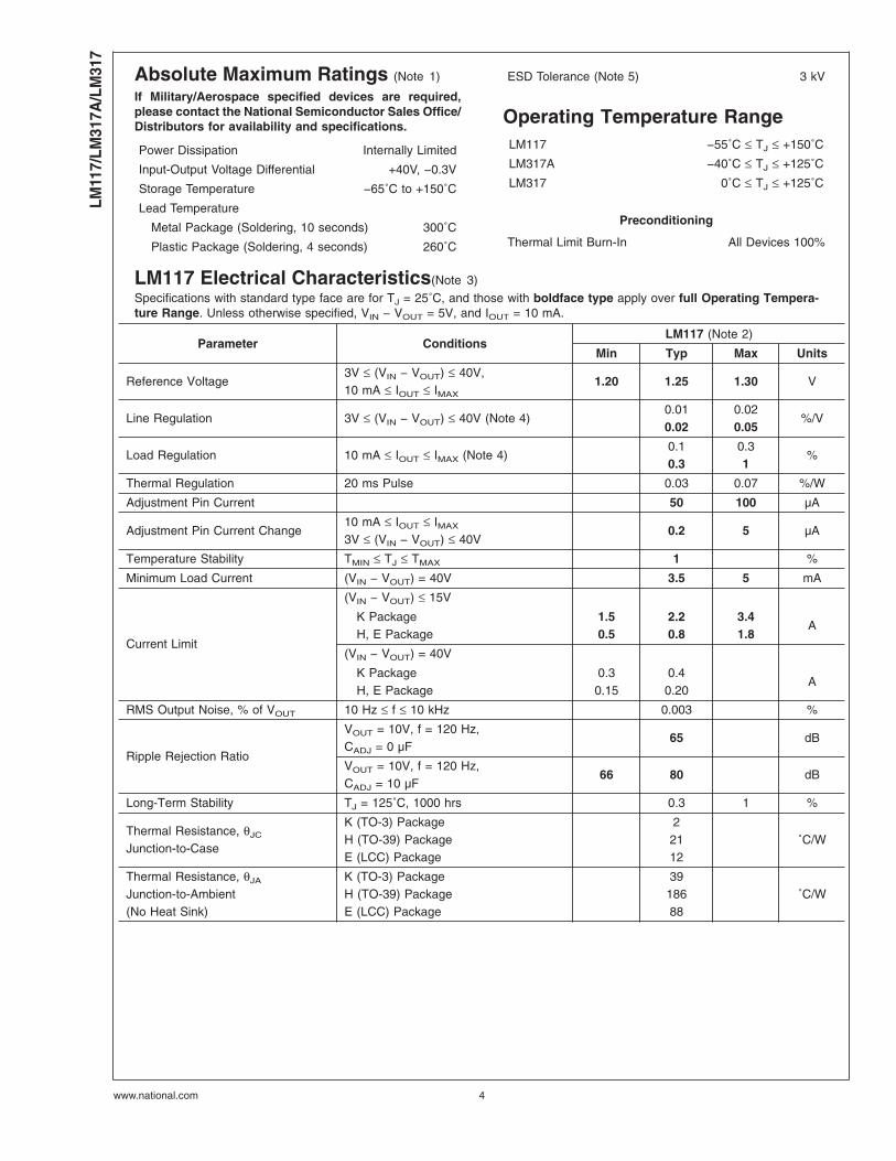
Ordering Information
PackageTemperature
RangeOutputCurrent
OrderNumber
PackageMarking
TransportMedia
NSCDrawing
TO-3Metal
Can (K)
−55˚C ≤ TJ ≤ +150˚C 1.5A LM117K STEEL LM117K STEEL P+ 50 Per BagK02A
0˚C ≤ TJ ≤ +125˚C 1.5A LM317K STEEL LM317K STEEL P+ 50 Per Bag
−55˚C ≤ TJ ≤ +150˚C 1.5A LM117K/883 LM117K/883 50 Per Bag K02C
TO-2203- Lead
−40˚C ≤ TJ ≤ +125˚C 1.5A LM317AT LM317AT P+ 45 Units/RailT03B
0˚C ≤ TJ ≤ +125˚C 1.5A LM317T LM317T P+ 45 Units/Rail
TO-2633- Lead
0˚C ≤ TJ ≤ +125˚C 1.5ALM317S
LM317S P+45 Units/Rail
TS3BLM317SX 500 Units Tape and Reel
SOT-2234- Lead
0˚C ≤ TJ ≤ +125˚C 1.0ALM317EMP
N01A1k Units Tape and Reel
MP04ALM317EMPX 2k Units Tape and Reel
−40˚C ≤ TJ ≤ +125˚C 1.0ALM317AEMP
N07A1k Units Tape and Reel
LM317AEMPX 2k Units Tape and Reel
TO-39Metal
Can (H)
−55˚C ≤ TJ ≤ +150˚C 0.5A LM117H LM117H P+ 500 Per Box
H03A−55˚C ≤ TJ ≤ +150˚C 0.5A LM117H/883 LM117H/883 20 Per Tray
−40˚C ≤ TJ ≤ +125˚C 0.5A LM317AH LM317AH P+ 500 Per Box
0˚C ≤ TJ ≤ +125˚C 0.5A LM317H LM317H P+ 500 Per Box
LCC −55˚C ≤ TJ ≤ +150˚C 0.5A LM117E/883 LM117E/883 50 Units/Rail E20A
TO-2523- LeadD-Pack
0˚C ≤ TJ ≤ +125˚C 0.5ALM317MDT
LM317MDT75 Units/Rail
TD03BLM317MDTX 2.5k Units Tape and Reel
−40˚C ≤ TJ ≤ +125˚C 0.5ALM317AMDT
LM317AMDT75 Units/Rail
LM317AMDTX 2.5k Units Tape and Reel
LM117/LM
317A/LM
317
www.national.com3
Absolute Maximum Ratings (Note 1)
If Military/Aerospace specified devices are required,please contact the National Semiconductor Sales Office/Distributors for availability and specifications.
Power Dissipation Internally Limited
Input-Output Voltage Differential +40V, −0.3V
Storage Temperature −65˚C to +150˚C
Lead Temperature
Metal Package (Soldering, 10 seconds) 300˚C
Plastic Package (Soldering, 4 seconds) 260˚C
ESD Tolerance (Note 5) 3 kV
Operating Temperature RangeLM117 −55˚C ≤ TJ ≤ +150˚C
LM317A −40˚C ≤ TJ ≤ +125˚C
LM317 0˚C ≤ TJ ≤ +125˚C
Preconditioning
Thermal Limit Burn-In All Devices 100%
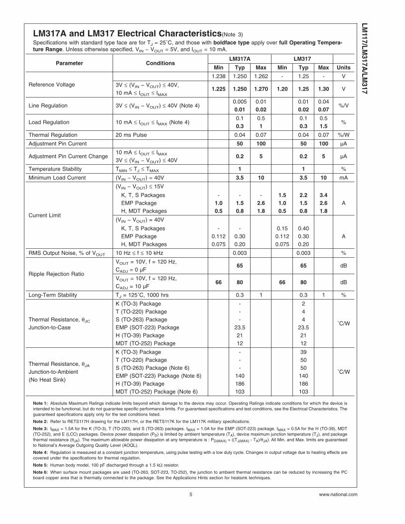
LM117 Electrical Characteristics(Note 3)
Specifications with standard type face are for TJ = 25˚C, and those with boldface type apply over full Operating Tempera-ture Range. Unless otherwise specified, VIN − VOUT = 5V, and IOUT = 10 mA.
Parameter ConditionsLM117 (Note 2)
Min Typ Max Units
Reference Voltage3V ≤ (VIN − VOUT) ≤ 40V,10 mA ≤ IOUT ≤ IMAX
1.20 1.25 1.30 V
Line Regulation 3V ≤ (VIN − VOUT) ≤ 40V (Note 4)0.010.02
0.020.05
%/V
Load Regulation 10 mA ≤ IOUT ≤ IMAX (Note 4)0.10.3
0.31
%
Thermal Regulation 20 ms Pulse 0.03 0.07 %/W
Adjustment Pin Current 50 100 µA
Adjustment Pin Current Change10 mA ≤ IOUT ≤ IMAX
3V ≤ (VIN − VOUT) ≤ 40V0.2 5 µA
Temperature Stability TMIN ≤ TJ ≤ TMAX 1 %
Minimum Load Current (VIN − VOUT) = 40V 3.5 5 mA
Current Limit
(VIN − VOUT) ≤ 15V
K PackageH, E Package
1.50.5
2.20.8
3.41.8
A
(VIN − VOUT) = 40V
K PackageH, E Package
0.30.15
0.40.20
A
RMS Output Noise, % of VOUT 10 Hz ≤ f ≤ 10 kHz 0.003 %
Ripple Rejection Ratio
VOUT = 10V, f = 120 Hz,CADJ = 0 µF
65 dB
VOUT = 10V, f = 120 Hz,CADJ = 10 µF
66 80 dB
Long-Term Stability TJ = 125˚C, 1000 hrs 0.3 1 %
Thermal Resistance, θJC
Junction-to-Case
K (TO-3) PackageH (TO-39) PackageE (LCC) Package
22112
˚C/W
Thermal Resistance, θJA
Junction-to-Ambient(No Heat Sink)
K (TO-3) PackageH (TO-39) PackageE (LCC) Package
3918688
˚C/W
LM11
7/LM
317A
/LM
317
www.national.com 4
LM317A and LM317 Electrical Characteristics(Note 3)
Specifications with standard type face are for TJ = 25˚C, and those with boldface type apply over full Operating Tempera-ture Range. Unless otherwise specified, VIN − VOUT = 5V, and IOUT = 10 mA.
Parameter ConditionsLM317A LM317
Min Typ Max Min Typ Max Units
Reference Voltage
1.238 1.250 1.262 - 1.25 - V
3V ≤ (VIN − VOUT) ≤ 40V,10 mA ≤ IOUT ≤ IMAX
1.225 1.250 1.270 1.20 1.25 1.30 V
Line Regulation 3V ≤ (VIN − VOUT) ≤ 40V (Note 4)0.0050.01
0.010.02
0.010.02
0.040.07
%/V
Load Regulation 10 mA ≤ IOUT ≤ IMAX (Note 4)0.10.3
0.51
0.10.3
0.51.5
%
Thermal Regulation 20 ms Pulse 0.04 0.07 0.04 0.07 %/W
Adjustment Pin Current 50 100 50 100 µA
Adjustment Pin Current Change10 mA ≤ IOUT ≤ IMAX
3V ≤ (VIN − VOUT) ≤ 40V0.2 5 0.2 5 µA
Temperature Stability TMIN ≤ TJ ≤ TMAX 1 1 %
Minimum Load Current (VIN − VOUT) = 40V 3.5 10 3.5 10 mA
Current Limit
(VIN − VOUT) ≤ 15V
K, T, S PackagesEMP PackageH, MDT Packages
-1.00.5
-1.50.8
-2.61.8
1.51.00.5
2.21.50.8
3.42.61.8
A
(VIN − VOUT) = 40V
K, T, S PackagesEMP PackageH, MDT Packages
-0.1120.075
-0.300.20
0.150.1120.075
0.400.300.20
A
RMS Output Noise, % of VOUT 10 Hz ≤ f ≤ 10 kHz 0.003 0.003 %
Ripple Rejection Ratio
VOUT = 10V, f = 120 Hz,CADJ = 0 µF
65 65 dB
VOUT = 10V, f = 120 Hz,CADJ = 10 µF
66 80 66 80 dB
Long-Term Stability TJ = 125˚C, 1000 hrs 0.3 1 0.3 1 %
Thermal Resistance, θJC
Junction-to-Case
K (TO-3) PackageT (TO-220) PackageS (TO-263) PackageEMP (SOT-223) PackageH (TO-39) PackageMDT (TO-252) Package
---
23.52112
244
23.52112
˚C/W
Thermal Resistance, θJA
Junction-to-Ambient(No Heat Sink)
K (TO-3) PackageT (TO-220) PackageS (TO-263) Package (Note 6)EMP (SOT-223) Package (Note 6)H (TO-39) PackageMDT (TO-252) Package (Note 6)
---
140186103
395050140186103
˚C/W
Note 1: Absolute Maximum Ratings indicate limits beyond which damage to the device may occur. Operating Ratings indicate conditions for which the device isintended to be functional, but do not guarantee specific performance limits. For guaranteed specifications and test conditions, see the Electrical Characteristics. Theguaranteed specifications apply only for the test conditions listed.
Note 2: Refer to RETS117H drawing for the LM117H, or the RETS117K for the LM117K military specifications.
Note 3: IMAX = 1.5A for the K (TO-3), T (TO-220), and S (TO-263) packages. IMAX = 1.0A for the EMP (SOT-223) package. IMAX = 0.5A for the H (TO-39), MDT(TO-252), and E (LCC) packages. Device power dissipation (PD) is limited by ambient temperature (TA), device maximum junction temperature (TJ), and packagethermal resistance (θJA). The maximum allowable power dissipation at any temperature is : PD(MAX) = ((TJ(MAX) - TA)/θJA). All Min. and Max. limits are guaranteedto National’s Average Outgoing Quality Level (AOQL).
Note 4: Regulation is measured at a constant junction temperature, using pulse testing with a low duty cycle. Changes in output voltage due to heating effects arecovered under the specifications for thermal regulation.
Note 5: Human body model, 100 pF discharged through a 1.5 kΩ resistor.
Note 6: When surface mount packages are used (TO-263, SOT-223, TO-252), the junction to ambient thermal resistance can be reduced by increasing the PCboard copper area that is thermally connected to the package. See the Applications Hints section for heatsink techniques.
LM117/LM
317A/LM
317
www.national.com5
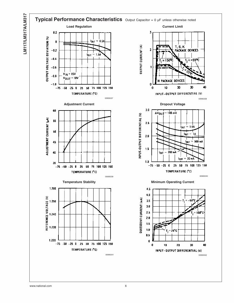
Typical Performance Characteristics Output Capacitor = 0 µF unless otherwise noted
Load Regulation Current Limit
00906337 00906338
Adjustment Current Dropout Voltage
00906339 00906340
Temperature Stability Minimum Operating Current
00906341 00906342
LM11
7/LM
317A
/LM
317
www.national.com 6
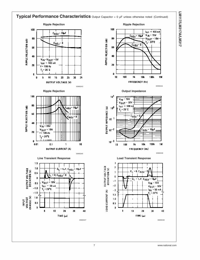
Typical Performance Characteristics Output Capacitor = 0 µF unless otherwise noted (Continued)
Ripple Rejection Ripple Rejection
00906343 00906344
Ripple Rejection Output Impedance
00906345 00906346
Line Transient Response Load Transient Response
00906347 00906348
LM117/LM
317A/LM
317
www.national.com7
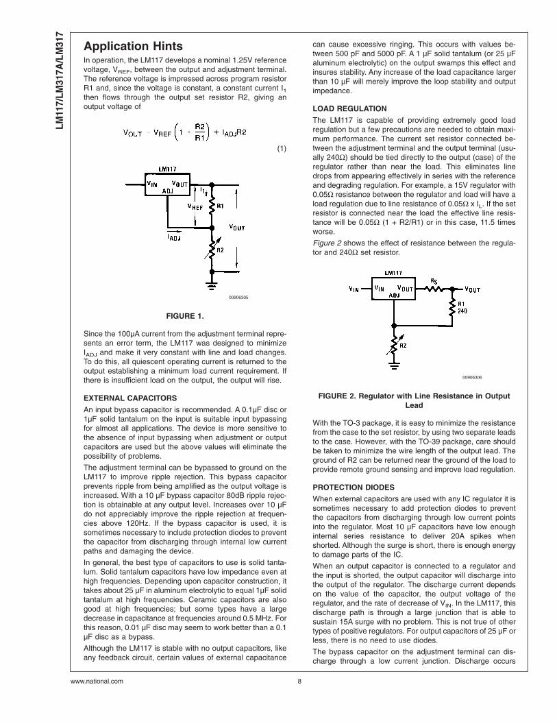
Application HintsIn operation, the LM117 develops a nominal 1.25V referencevoltage, VREF, between the output and adjustment terminal.The reference voltage is impressed across program resistorR1 and, since the voltage is constant, a constant current I1then flows through the output set resistor R2, giving anoutput voltage of
(1)
Since the 100µA current from the adjustment terminal repre-sents an error term, the LM117 was designed to minimizeIADJ and make it very constant with line and load changes.To do this, all quiescent operating current is returned to theoutput establishing a minimum load current requirement. Ifthere is insufficient load on the output, the output will rise.
EXTERNAL CAPACITORS
An input bypass capacitor is recommended. A 0.1µF disc or1µF solid tantalum on the input is suitable input bypassingfor almost all applications. The device is more sensitive tothe absence of input bypassing when adjustment or outputcapacitors are used but the above values will eliminate thepossibility of problems.
The adjustment terminal can be bypassed to ground on theLM117 to improve ripple rejection. This bypass capacitorprevents ripple from being amplified as the output voltage isincreased. With a 10 µF bypass capacitor 80dB ripple rejec-tion is obtainable at any output level. Increases over 10 µFdo not appreciably improve the ripple rejection at frequen-cies above 120Hz. If the bypass capacitor is used, it issometimes necessary to include protection diodes to preventthe capacitor from discharging through internal low currentpaths and damaging the device.
In general, the best type of capacitors to use is solid tanta-lum. Solid tantalum capacitors have low impedance even athigh frequencies. Depending upon capacitor construction, ittakes about 25 µF in aluminum electrolytic to equal 1µF solidtantalum at high frequencies. Ceramic capacitors are alsogood at high frequencies; but some types have a largedecrease in capacitance at frequencies around 0.5 MHz. Forthis reason, 0.01 µF disc may seem to work better than a 0.1µF disc as a bypass.
Although the LM117 is stable with no output capacitors, likeany feedback circuit, certain values of external capacitance
can cause excessive ringing. This occurs with values be-tween 500 pF and 5000 pF. A 1 µF solid tantalum (or 25 µFaluminum electrolytic) on the output swamps this effect andinsures stability. Any increase of the load capacitance largerthan 10 µF will merely improve the loop stability and outputimpedance.
LOAD REGULATION
The LM117 is capable of providing extremely good loadregulation but a few precautions are needed to obtain maxi-mum performance. The current set resistor connected be-tween the adjustment terminal and the output terminal (usu-ally 240Ω) should be tied directly to the output (case) of theregulator rather than near the load. This eliminates linedrops from appearing effectively in series with the referenceand degrading regulation. For example, a 15V regulator with0.05Ω resistance between the regulator and load will have aload regulation due to line resistance of 0.05Ω x IL. If the setresistor is connected near the load the effective line resis-tance will be 0.05Ω (1 + R2/R1) or in this case, 11.5 timesworse.
Figure 2 shows the effect of resistance between the regula-tor and 240Ω set resistor.
With the TO-3 package, it is easy to minimize the resistancefrom the case to the set resistor, by using two separate leadsto the case. However, with the TO-39 package, care shouldbe taken to minimize the wire length of the output lead. Theground of R2 can be returned near the ground of the load toprovide remote ground sensing and improve load regulation.
PROTECTION DIODES
When external capacitors are used with any IC regulator it issometimes necessary to add protection diodes to preventthe capacitors from discharging through low current pointsinto the regulator. Most 10 µF capacitors have low enoughinternal series resistance to deliver 20A spikes whenshorted. Although the surge is short, there is enough energyto damage parts of the IC.
When an output capacitor is connected to a regulator andthe input is shorted, the output capacitor will discharge intothe output of the regulator. The discharge current dependson the value of the capacitor, the output voltage of theregulator, and the rate of decrease of VIN. In the LM117, thisdischarge path is through a large junction that is able tosustain 15A surge with no problem. This is not true of othertypes of positive regulators. For output capacitors of 25 µF orless, there is no need to use diodes.
The bypass capacitor on the adjustment terminal can dis-charge through a low current junction. Discharge occurs
00906305
FIGURE 1.
00906306
FIGURE 2. Regulator with Line Resistance in OutputLead
LM11
7/LM
317A
/LM
317
www.national.com 8
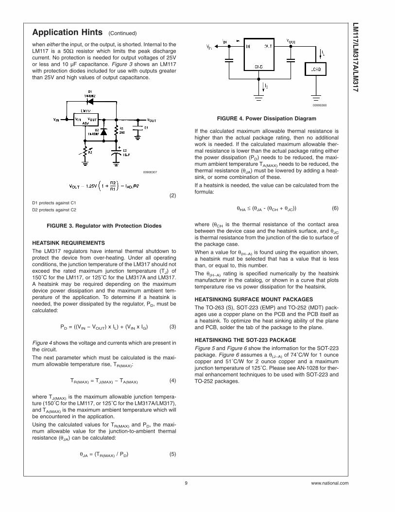
Application Hints (Continued)
when either the input, or the output, is shorted. Internal to theLM117 is a 50Ω resistor which limits the peak dischargecurrent. No protection is needed for output voltages of 25Vor less and 10 µF capacitance. Figure 3 shows an LM117with protection diodes included for use with outputs greaterthan 25V and high values of output capacitance.
HEATSINK REQUIREMENTS
The LM317 regulators have internal thermal shutdown toprotect the device from over-heating. Under all operatingconditions, the junction temperature of the LM317 should notexceed the rated maximum junction temperature (TJ) of150˚C for the LM117, or 125˚C for the LM317A and LM317.A heatsink may be required depending on the maximumdevice power dissipation and the maximum ambient tem-perature of the application. To determine if a heatsink isneeded, the power dissipated by the regulator, PD, must becalculated:
PD = ((VIN − VOUT) x IL) + (VIN x IG) (3)
Figure 4 shows the voltage and currents which are present inthe circuit.
The next parameter which must be calculated is the maxi-mum allowable temperature rise, TR(MAX):
TR(MAX) = TJ(MAX) − TA(MAX) (4)
where TJ(MAX) is the maximum allowable junction tempera-ture (150˚C for the LM117, or 125˚C for the LM317A/LM317),and TA(MAX) is the maximum ambient temperature which willbe encountered in the application.
Using the calculated values for TR(MAX) and PD, the maxi-mum allowable value for the junction-to-ambient thermalresistance (θJA) can be calculated:
θJA = (TR(MAX) / PD) (5)
If the calculated maximum allowable thermal resistance ishigher than the actual package rating, then no additionalwork is needed. If the calculated maximum allowable ther-mal resistance is lower than the actual package rating eitherthe power dissipation (PD) needs to be reduced, the maxi-mum ambient temperature TA(MAX) needs to be reduced, thethermal resistance (θJA) must be lowered by adding a heat-sink, or some combination of these.
If a heatsink is needed, the value can be calculated from theformula:
θHA ≤ (θJA - (θCH + θJC)) (6)
where (θCH is the thermal resistance of the contact areabetween the device case and the heatsink surface, and θJC
is thermal resistance from the junction of the die to surface ofthe package case.
When a value for θ(H−A) is found using the equation shown,a heatsink must be selected that has a value that is lessthan, or equal to, this number.
The θ(H−A) rating is specified numerically by the heatsinkmanufacturer in the catalog, or shown in a curve that plotstemperature rise vs power dissipation for the heatsink.
HEATSINKING SURFACE MOUNT PACKAGES
The TO-263 (S), SOT-223 (EMP) and TO-252 (MDT) pack-ages use a copper plane on the PCB and the PCB itself asa heatsink. To optimize the heat sinking ability of the planeand PCB, solder the tab of the package to the plane.
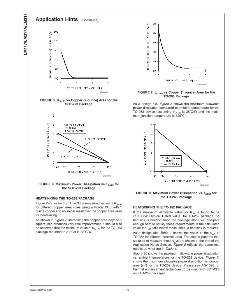
HEATSINKING THE SOT-223 PACKAGE
Figure 5 and Figure 6 show the information for the SOT-223package. Figure 6 assumes a θ(J−A) of 74˚C/W for 1 ouncecopper and 51˚C/W for 2 ounce copper and a maximumjunction temperature of 125˚C. Please see AN-1028 for ther-mal enhancement techniques to be used with SOT-223 andTO-252 packages.
00906307
(2)D1 protects against C1
D2 protects against C2
FIGURE 3. Regulator with Protection Diodes
00906360
FIGURE 4. Power Dissipation Diagram
LM117/LM
317A/LM
317
www.national.com9
Application Hints (Continued)
HEATSINKING THE TO-263 PACKAGE
Figure 7 shows for the TO-263 the measured values of θ(J−A)
for different copper area sizes using a typical PCB with 1ounce copper and no solder mask over the copper area usedfor heatsinking.
As shown in Figure 7, increasing the copper area beyond 1square inch produces very little improvement. It should alsobe observed that the minimum value of θ(J−A) for the TO-263package mounted to a PCB is 32˚C/W.
As a design aid, Figure 8 shows the maximum allowablepower dissipation compared to ambient temperature for theTO-263 device (assuming θ(J−A) is 35˚C/W and the maxi-mum junction temperature is 125˚C).
HEATSINKING THE TO-252 PACKAGE
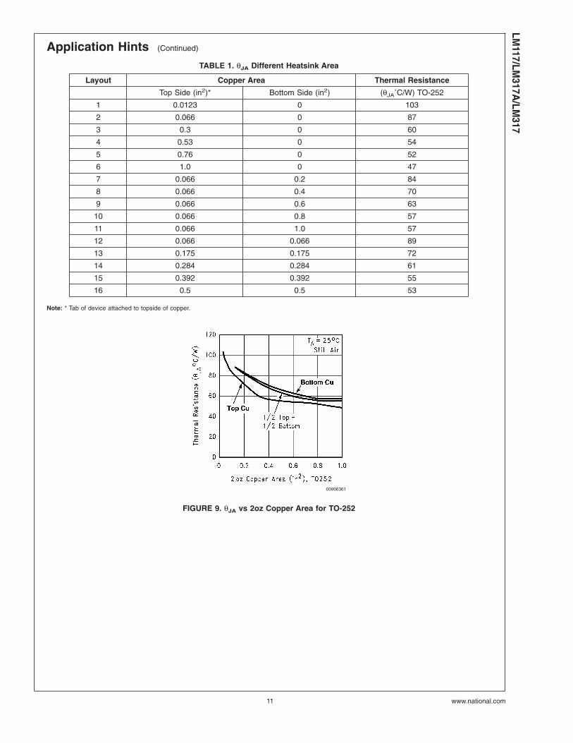
If the maximum allowable value for θJA is found to be≥103˚C/W (Typical Rated Value) for TO-252 package, noheatsink is needed since the package alone will dissipateenough heat to satisfy these requirements. If the calculatedvalue for θJA falls below these limits, a heatsink is required.
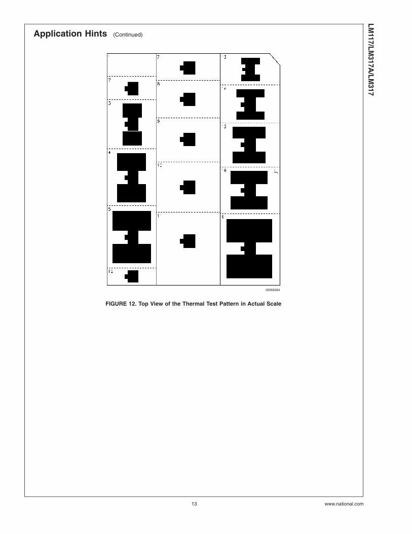
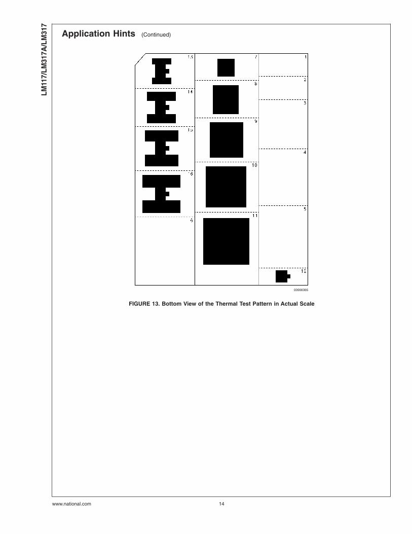
As a design aid, Table 1 shows the value of the θJA ofTO-252 for different heatsink area. The copper patterns thatwe used to measure these θJAs are shown at the end of theApplication Notes Section. Figure 9 reflects the same testresults as what are in Table 1.
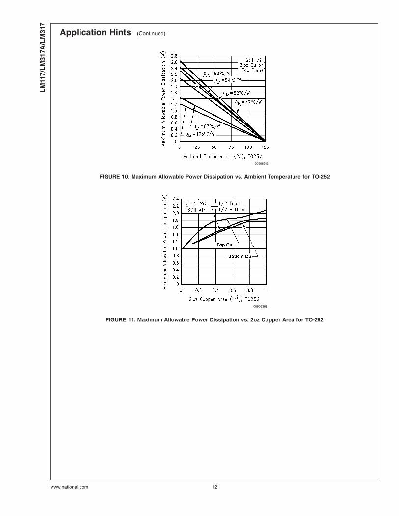
Figure 10 shows the maximum allowable power dissipationvs. ambient temperature for the TO-252 device. Figure 11shows the maximum allowable power dissipation vs. copperarea (in2) for the TO-252 device. Please see AN-1028 forthermal enhancement techniques to be used with SOT-223and TO-252 packages.
00906357
FIGURE 5. θ(J−A) vs Copper (2 ounce) Area for theSOT-223 Package
00906358
FIGURE 6. Maximum Power Dissipation vs TAMB forthe SOT-223 Package
00906355
FIGURE 7. θ(J−A) vs Copper (1 ounce) Area for theTO-263 Package
00906356
FIGURE 8. Maximum Power Dissipation vs TAMB forthe TO-263 Package
LM11
7/LM
317A
/LM
317
www.national.com 10
Application Hints (Continued)
TABLE 1. θJA Different Heatsink Area
Layout Copper Area Thermal Resistance
Top Side (in2)* Bottom Side (in2) (θJA˚C/W) TO-252
1 0.0123 0 103
2 0.066 0 87
3 0.3 0 60
4 0.53 0 54
5 0.76 0 52
6 1.0 0 47
7 0.066 0.2 84
8 0.066 0.4 70
9 0.066 0.6 63
10 0.066 0.8 57
11 0.066 1.0 57
12 0.066 0.066 89
13 0.175 0.175 72
14 0.284 0.284 61
15 0.392 0.392 55
16 0.5 0.5 53
Note: * Tab of device attached to topside of copper.
00906361
FIGURE 9. θJA vs 2oz Copper Area for TO-252
LM117/LM
317A/LM
317
www.national.com11
Application Hints (Continued)
00906363
FIGURE 10. Maximum Allowable Power Dissipation vs. Ambient Temperature for TO-252
00906362
FIGURE 11. Maximum Allowable Power Dissipation vs. 2oz Copper Area for TO-252
LM11
7/LM
317A
/LM
317
www.national.com 12
Application Hints (Continued)
00906364
FIGURE 12. Top View of the Thermal Test Pattern in Actual Scale
LM117/LM
317A/LM
317
www.national.com13
Application Hints (Continued)
00906365
FIGURE 13. Bottom View of the Thermal Test Pattern in Actual Scale
LM11
7/LM
317A
/LM
317
www.national.com 14
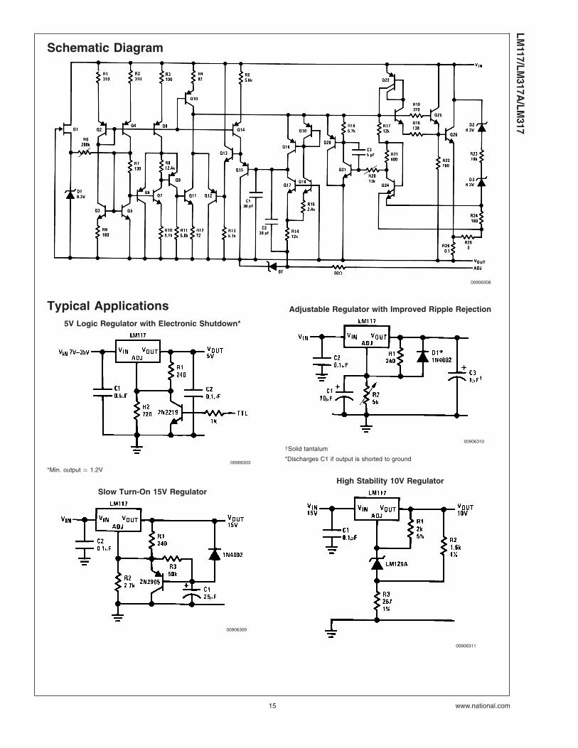
Schematic Diagram
00906308
Typical Applications5V Logic Regulator with Electronic Shutdown*
00906303
*Min. output ) 1.2V
Slow Turn-On 15V Regulator
00906309
Adjustable Regulator with Improved Ripple Rejection
00906310
†Solid tantalum
*Discharges C1 if output is shorted to ground
High Stability 10V Regulator
00906311
LM117/LM
317A/LM
317
www.national.com15
Typical Applications (Continued)
High Current Adjustable Regulator
00906312
‡Optional — improves ripple rejection
†Solid tantalum
*Minimum load current = 30 mA
0 to 30V Regulator
00906313
Full output current not available at high input-output voltages
Power Follower
00906314
LM11
7/LM
317A
/LM
317
www.national.com 16
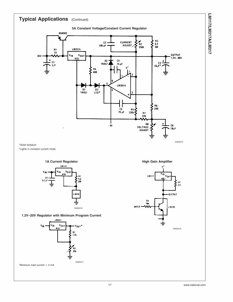
Typical Applications (Continued)
5A Constant Voltage/Constant Current Regulator
00906315
†Solid tantalum
*Lights in constant current mode
1A Current Regulator
00906316
1.2V–20V Regulator with Minimum Program Current
00906317
*Minimum load current ) 4 mA
High Gain Amplifier
00906318
LM117/LM
317A/LM
317
www.national.com17
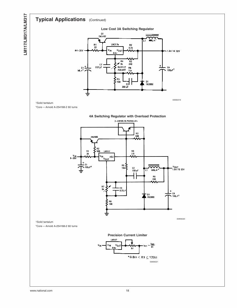
Typical Applications (Continued)
Low Cost 3A Switching Regulator
00906319
†Solid tantalum
*Core — Arnold A-254168-2 60 turns
4A Switching Regulator with Overload Protection
00906320
†Solid tantalum
*Core — Arnold A-254168-2 60 turns
Precision Current Limiter
00906321
LM11
7/LM
317A
/LM
317
www.national.com 18
Typical Applications (Continued)
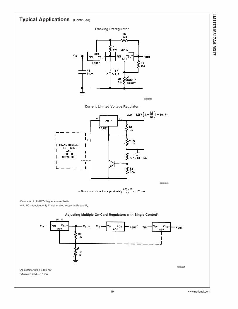
Tracking Preregulator
00906322
Current Limited Voltage Regulator
00906323
(Compared to LM117’s higher current limit)
— At 50 mA output only 3⁄4 volt of drop occurs in R3 and R4
Adjusting Multiple On-Card Regulators with Single Control*
00906324
*All outputs within ±100 mV
†Minimum load — 10 mA
LM117/LM
317A/LM
317
www.national.com19
Typical Applications (Continued)
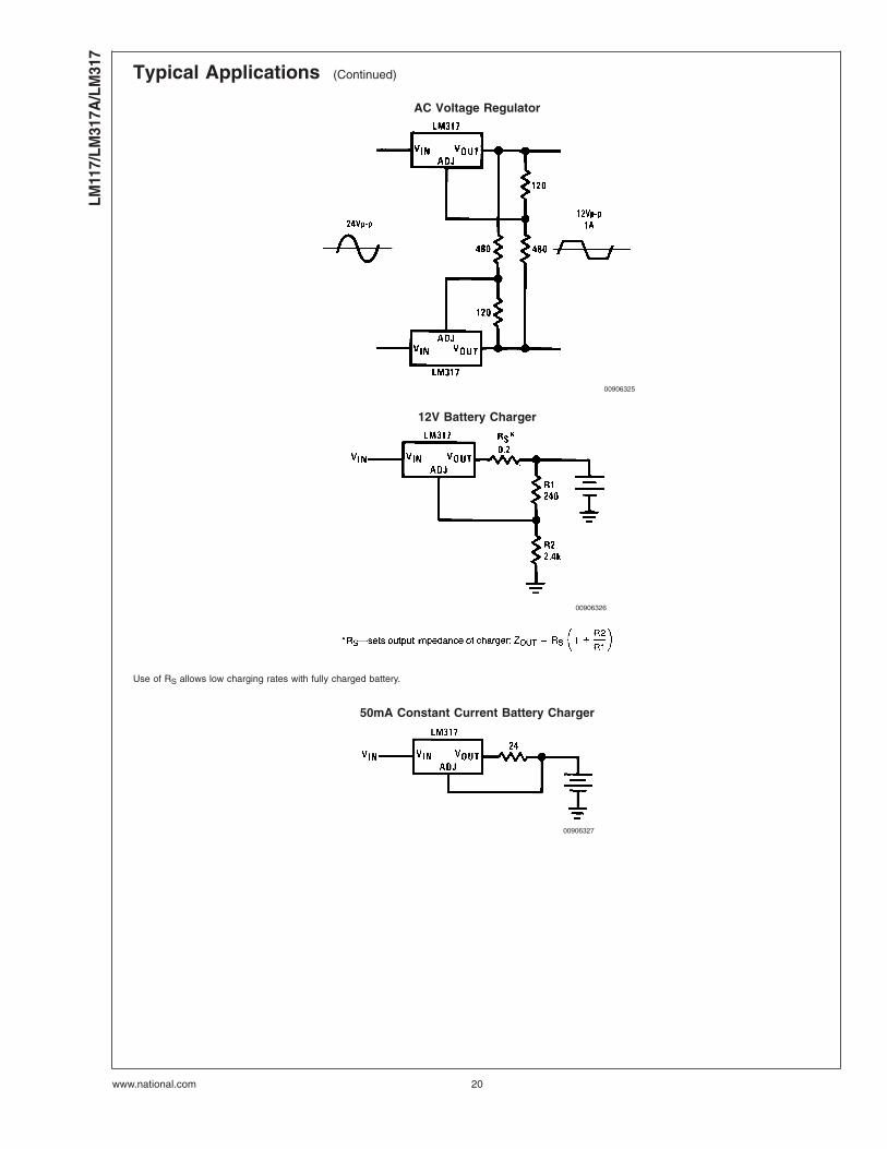
AC Voltage Regulator
00906325
12V Battery Charger
00906326
Use of RS allows low charging rates with fully charged battery.
50mA Constant Current Battery Charger
00906327
LM11
7/LM
317A
/LM
317
www.national.com 20
Typical Applications (Continued)
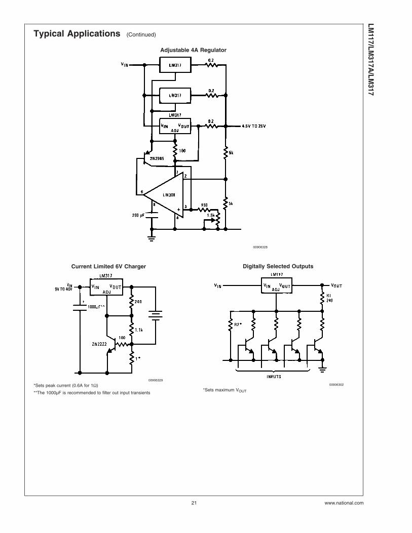
Adjustable 4A Regulator
00906328
Current Limited 6V Charger
00906329
*Sets peak current (0.6A for 1Ω)
**The 1000µF is recommended to filter out input transients
Digitally Selected Outputs
00906302
*Sets maximum VOUT
LM117/LM
317A/LM
317
www.national.com21
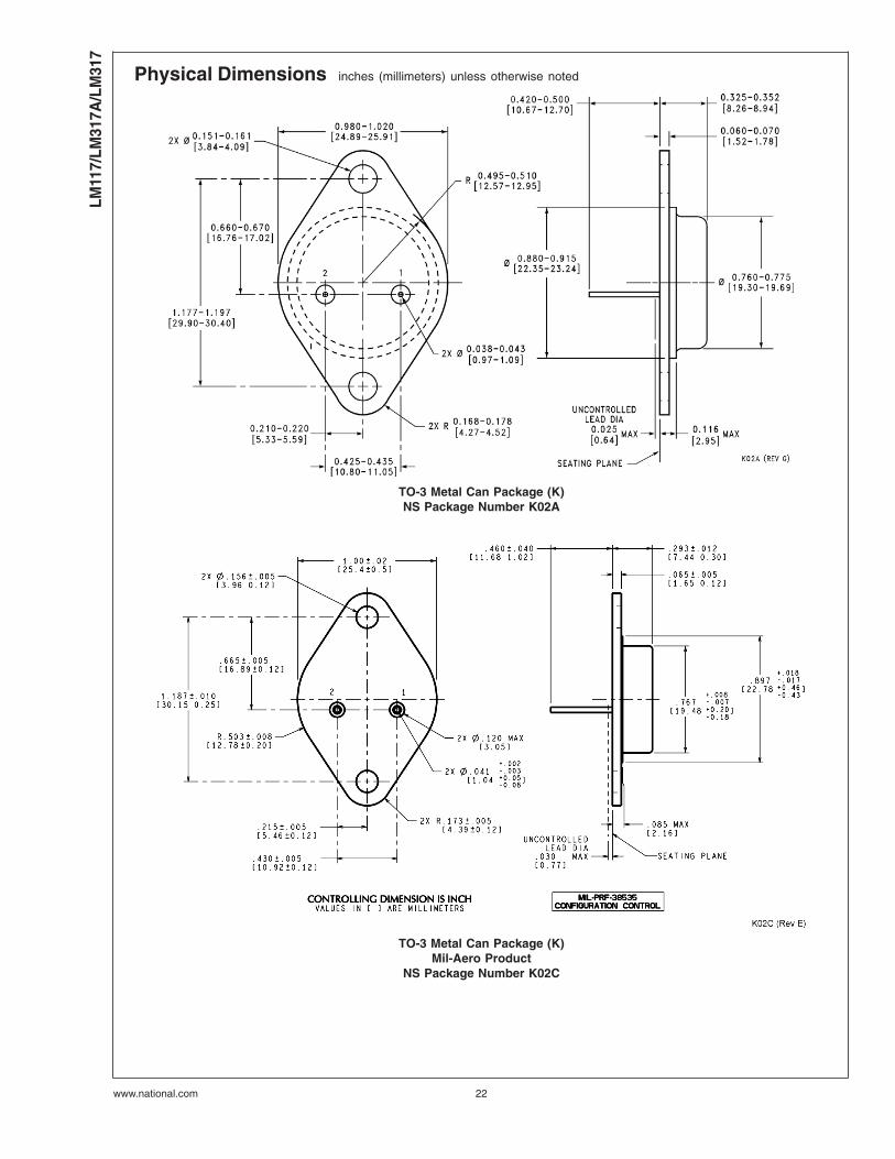
Physical Dimensions inches (millimeters) unless otherwise noted
TO-3 Metal Can Package (K)NS Package Number K02A
TO-3 Metal Can Package (K)Mil-Aero Product
NS Package Number K02C
LM11
7/LM
317A
/LM
317
www.national.com 22
Physical Dimensions inches (millimeters) unless otherwise noted (Continued)
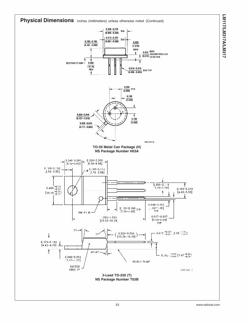
TO-39 Metal Can Package (H)NS Package Number H03A
3-Lead TO-220 (T)NS Package Number T03B
LM117/LM
317A/LM
317
www.national.com23
Physical Dimensions inches (millimeters) unless otherwise noted (Continued)
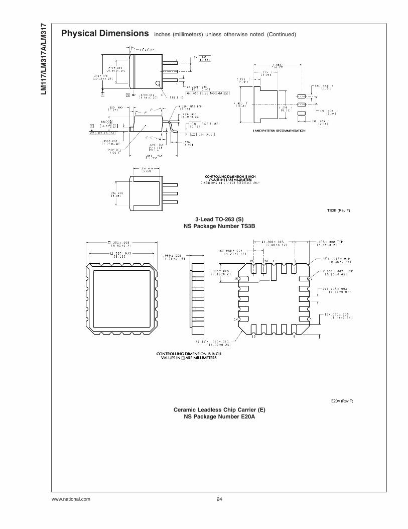
3-Lead TO-263 (S)NS Package Number TS3B
Ceramic Leadless Chip Carrier (E)NS Package Number E20A
LM11
7/LM
317A
/LM
317
www.national.com 24
Physical Dimensions inches (millimeters) unless otherwise noted (Continued)
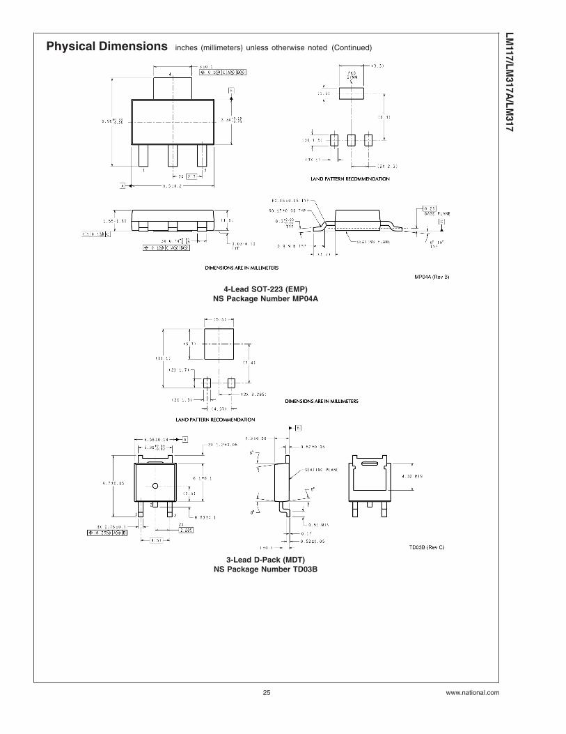
4-Lead SOT-223 (EMP)NS Package Number MP04A
3-Lead D-Pack (MDT)NS Package Number TD03B
LM117/LM
317A/LM
317
www.national.com25
Notes
National does not assume any responsibility for use of any circuitry described, no circuit patent licenses are implied and National reservesthe right at any time without notice to change said circuitry and specifications.
For the most current product information visit us at www.national.com.
LIFE SUPPORT POLICY
NATIONAL’S PRODUCTS ARE NOT AUTHORIZED FOR USE AS CRITICAL COMPONENTS IN LIFE SUPPORT DEVICES OR SYSTEMSWITHOUT THE EXPRESS WRITTEN APPROVAL OF THE PRESIDENT AND GENERAL COUNSEL OF NATIONAL SEMICONDUCTORCORPORATION. As used herein:
1. Life support devices or systems are devices or systemswhich, (a) are intended for surgical implant into the body, or(b) support or sustain life, and whose failure to perform whenproperly used in accordance with instructions for useprovided in the labeling, can be reasonably expected to resultin a significant injury to the user.
2. A critical component is any component of a life supportdevice or system whose failure to perform can be reasonablyexpected to cause the failure of the life support device orsystem, or to affect its safety or effectiveness.
BANNED SUBSTANCE COMPLIANCE
National Semiconductor follows the provisions of the Product Stewardship Guide for Customers (CSP-9-111C2) and Banned Substancesand Materials of Interest Specification (CSP-9-111S2) for regulatory environmental compliance. Details may be found at:www.national.com/quality/green.
Lead free products are RoHS compliant.
National SemiconductorAmericas CustomerSupport CenterEmail: [email protected]: 1-800-272-9959
National SemiconductorEurope Customer Support Center
Fax: +49 (0) 180-530 85 86Email: [email protected]
Deutsch Tel: +49 (0) 69 9508 6208English Tel: +44 (0) 870 24 0 2171Français Tel: +33 (0) 1 41 91 8790
National SemiconductorAsia Pacific CustomerSupport CenterEmail: [email protected]
National SemiconductorJapan Customer Support CenterFax: 81-3-5639-7507Email: [email protected]: 81-3-5639-7560
www.national.com
LM11
7/LM
317A
/LM
317
3-Te
rmin
alA
djus
tabl
eR
egul
ator