LM1036 Dual DC Operated Tone/Volume/Balance Circuit … control IC.pdf · LM1036 Dual DC Operated...
27
LM1036 www.ti.com SNAS525C – JAN 1995 – REVISED APRIL 2013 LM1036 Dual DC Operated Tone/Volume/Balance Circuit Check for Samples: LM1036 1FEATURES DESCRIPTION The LM1036 is a DC controlled tone (bass/treble), 2• Wide Supply Voltage Range, 9V to 16V volume and balance circuit for stereo applications in • Large Volume Control Range, 75 dB Typical car radio, TV and audio systems. An additional • Tone Control, ±15 dB Typical control input allows loudness compensation to be simply effected. • Channel Separation, 75 dB Typical • Low Distortion, 0.06% Typical for An Input Four control inputs provide control of the bass, treble, balance and volume functions through application of Level of 0.3 Vrms DC voltages from a remote control system or, • High Signal to Noise, 80 dB Typical for an alternatively, from four potentiometers which may be Input Level of 0.3 Vrms biased from a zener regulated supply provided on the • Few External Components Required circuit. Each tone response is defined by a single capacitor chosen to give the desired characteristic. Block and Connection Diagram Figure 1. PDIP and SOIC Packages See Package Numbers NFH0020A or DW0020B 1 Please be aware that an important notice concerning availability, standard warranty, and use in critical applications of Texas Instruments semiconductor products and disclaimers thereto appears at the end of this data sheet. 2All trademarks are the property of their respective owners. PRODUCTION DATA information is current as of publication date. Copyright © 1995–2013, Texas Instruments Incorporated Products conform to specifications per the terms of the Texas Instruments standard warranty. Production processing does not necessarily include testing of all parameters.
Transcript of LM1036 Dual DC Operated Tone/Volume/Balance Circuit … control IC.pdf · LM1036 Dual DC Operated...

LM1036
www.ti.com SNAS525C –JAN 1995–REVISED APRIL 2013
LM1036 Dual DC Operated Tone/Volume/Balance CircuitCheck for Samples: LM1036
1FEATURES DESCRIPTIONThe LM1036 is a DC controlled tone (bass/treble),
2• Wide Supply Voltage Range, 9V to 16Vvolume and balance circuit for stereo applications in
• Large Volume Control Range, 75 dB Typical car radio, TV and audio systems. An additional• Tone Control, ±15 dB Typical control input allows loudness compensation to be
simply effected.• Channel Separation, 75 dB Typical• Low Distortion, 0.06% Typical for An Input Four control inputs provide control of the bass, treble,
balance and volume functions through application ofLevel of 0.3 VrmsDC voltages from a remote control system or,• High Signal to Noise, 80 dB Typical for analternatively, from four potentiometers which may beInput Level of 0.3 Vrmsbiased from a zener regulated supply provided on the
• Few External Components Required circuit.
Each tone response is defined by a single capacitorchosen to give the desired characteristic.
Block and Connection Diagram
Figure 1. PDIP and SOIC PackagesSee Package Numbers NFH0020A or DW0020B
1
Please be aware that an important notice concerning availability, standard warranty, and use in critical applications ofTexas Instruments semiconductor products and disclaimers thereto appears at the end of this data sheet.
2All trademarks are the property of their respective owners.
PRODUCTION DATA information is current as of publication date. Copyright © 1995–2013, Texas Instruments IncorporatedProducts conform to specifications per the terms of the TexasInstruments standard warranty. Production processing does notnecessarily include testing of all parameters.

LM1036
SNAS525C –JAN 1995–REVISED APRIL 2013 www.ti.com
These devices have limited built-in ESD protection. The leads should be shorted together or the device placed in conductive foamduring storage or handling to prevent electrostatic damage to the MOS gates.
Absolute Maximum Ratings (1) (2)
Supply Voltage 16V
Control Pin Voltage (Pins 4, 7, 9, 12, 14) VCC
Operating Temperature Range 0°C to +70°C
Storage Temperature Range −65°C to +150°C
Power Dissipation 1W
Lead Temp. (Soldering, 10 seconds) 260°C
(1) Absolute Maximum Ratings indicate limits beyond which damage to the device may occur. Operating Ratings indicate conditions forwhich the device is functional, but do not ensure specific performance limits.
(2) If Military/Aerospace specified devices are required, please contact the Texas Instruments Sales Office/ Distributors for availability andspecifications.
Electrical Characteristics (1)
VCC=12V, TA=25°C (unless otherwise stated)
Parameter Conditions Min Typ Max Units
Supply Voltage Range Pin 11 9 16 V
Supply Current 35 45 mA
Zener Regulated Output Pin 17
Voltage 5.4 V
Current 5 mA
Maximum Output Voltage Pins 8, 13; f=1 kHz
VCC=9V, Maximum Gain 0.8 Vrms
VCC=12V 0.8 1.0 Vrms
Maximum Input Voltage Pins 2, 19; f=1 kHz, VCC 2V 1.3 1.6 Vrms
Gain=−10 dB
Input Resistance Pins 2, 19; f=1 kHz 20 30 kΩOutput Resistance Pins 8, 13; f=1 kHz 20 ΩMaximum Gain V(Pin 12)=V(Pin 17); f=1 kHz −2 0 2 dB
Volume Control Range f=1 kHz 70 75 dB
Gain Tracking f=1 kHz
Channel 1–Channel 2 0 dB through −40 dB 1 3 dB
−40 dB through −60 dB 2 dB
Balance Control Range Pins 8, 13; f=1 kHz 1 dB
−26 −20 dB
Bass Control Range (2) f=40 Hz, Cb=0.39 μF
V(Pin 14)=V(Pin 17) 12 15 18 dB
V(Pin 14)=0V −12 −15 −18 dB
Treble Control Range (2) f= 16 kHz, Ct,=0.01 μF
V(Pin 4)=V(Pin 17) 12 15 18 dB
V(Pin 4)=0V −12 −15 −18 dB
Total Harmonic Distortion f=1 kHz, VIN=0.3 Vrms
Gain=0 dB 0.06 0.3 %
Gain=−30 dB 0.03 %
Channel Separation f=1 kHz, Maximum Gain 60 75 dB
(1) The maximum permissible input level is dependent on tone and volume settings. See Application Notes.(2) The tone control range is defined by capacitors Cb and Ct. See Application Notes.
2 Submit Documentation Feedback Copyright © 1995–2013, Texas Instruments Incorporated
Product Folder Links: LM1036

LM1036
www.ti.com SNAS525C –JAN 1995–REVISED APRIL 2013
Electrical Characteristics(1) (continued)VCC=12V, TA=25°C (unless otherwise stated)
Parameter Conditions Min Typ Max Units
Signal/Noise Ratio Unweighted 100 Hz–20 kHz 80 dB
Maximum Gain, 0 dB=0.3 Vrms
CCIR/ARM (3)
Gain=0 dB, VIN=0.3 Vrms 75 79 dB
Gain=−20 dB, VIN=1.0 Vrms 72 dB
Output Noise Voltage at Minimum Gain CCIR/ARM (3) 10 16 μV
Supply Ripple Rejection 200 mVrms, 1 kHz Ripple 35 50 dB
Control Input Currents Pins 4, 7, 9, 12, 14 (V=0V) −0.6 −2.5 μA
Frequency Response −1 dB (Flat Response 250 kHz
20 Hz–16 kHz)
(3) Gaussian noise, measured over a period of 50 ms per channel, with a CCIR filter referenced to 2 kHz and an average-respondingmeter.
Copyright © 1995–2013, Texas Instruments Incorporated Submit Documentation Feedback 3
Product Folder Links: LM1036

LM1036
SNAS525C –JAN 1995–REVISED APRIL 2013 www.ti.com
Typical Performance Characteristics
Volume Control Characteristics Balance Control Characteristic
Figure 2. Figure 3.
Tone Control Characteristic Tone Characteristic (Gain vs Frequency)
Figure 4. Figure 5.
Tone Characteristic (Gain vs Frequency) Loudness Compensated Volume Characteristic
Figure 6. Figure 7.
4 Submit Documentation Feedback Copyright © 1995–2013, Texas Instruments Incorporated
Product Folder Links: LM1036

LM1036
www.ti.com SNAS525C –JAN 1995–REVISED APRIL 2013
Typical Performance Characteristics (continued)Input Signal Handling vs Supply Voltage THD vs Gain
Figure 8. Figure 9.
Channel Separation vs Frequency Loudness Control Characteristic
Figure 10. Figure 11.
Output Noise Voltage vs Gain THD vs Input Voltage
Figure 12. Figure 13.
Copyright © 1995–2013, Texas Instruments Incorporated Submit Documentation Feedback 5
Product Folder Links: LM1036

LM1036
SNAS525C –JAN 1995–REVISED APRIL 2013 www.ti.com
Application Notes
TONE RESPONSE
The maximum boost and cut can be optimized for individual applications by selection of the appropriate values ofCt (treble) and Cb (bass).
The tone responses are defined by the relationships:
where• ab=at=0 for maximum bass and treble boost respectively• ab=at=1 for maximum cut (1)
For the values of Cb and Ct of 0.39 μF and 0.01 μF as shown in the Application Circuit, 15 dB of boost or cut isobtained at 40 Hz and 16 kHz.
ZENER VOLTAGE
A zener voltage (pin 17=5.4V) is provided which may be used to bias the control potentiometers. Setting a DClevel of one half of the zener voltage on the control inputs, pins 4, 9, and 14, results in the balanced gain and flatresponse condition. Typical spread on the zener voltage is ±100 mV and this must be taken into account ifcontrol signals are used which are not referenced to the zener voltage. If this is the case, then they will need tobe derived with similar accuracy.
LOUDNESS COMPENSATION
A simple loudness compensation may be effected by applying a DC control voltage to pin 7. This operates on thetone control stages to produce an additional boost limited by the maximum boost defined by Cb and Ct. There isno loudness compensation when pin 7 is connected to pin 17. Pin 7 can be connected to pin 12 to give theloudness compensated volume characteristic as illustrated without the addition of further external components.(Tone settings are for flat response, Cb and Ct as given in Application Circuit.) Modification to the loudnesscharacteristic is possible by changing the capacitors Cb and Ct for a different basic response or, by a resistornetwork between pins 7 and 12 for a different threshold and slope.
SIGNAL HANDLING
The volume control function of the LM1036 is carried out in two stages, controlled by the DC voltage on pin 12,to improve signal handling capability and provide a reduction of output noise level at reduced gain. The firststage is before the tone control processing and provides an initial 15 dB of gain reduction, so ensuring that thetone sections are not overdriven by large input levels when operating with a low volume setting. Any combinationof tone and volume settings may be used provided the output level does not exceed 1 Vrms, VCC=12V (0.8 Vrms,VCC=9V). At reduced gain (<−6 dB) the input stage will overload if the input level exceeds 1.6 Vrms, VCC=12V(1.1Vrms, VCC=9V). As there is volume control on the input stages, the inputs may be operated with a lower overloadmargin than would otherwise be acceptable, allowing a possible improvement in signal to noise ratio.
6 Submit Documentation Feedback Copyright © 1995–2013, Texas Instruments Incorporated
Product Folder Links: LM1036

LM1036
www.ti.com SNAS525C –JAN 1995–REVISED APRIL 2013
Application Circuit
Copyright © 1995–2013, Texas Instruments Incorporated Submit Documentation Feedback 7
Product Folder Links: LM1036

LM1036
SNAS525C –JAN 1995–REVISED APRIL 2013 www.ti.com
APPLICATIONS INFORMATION
OBTAINING MODIFIED RESPONSE CURVES
The LM1036 is a dual DC controlled bass, treble, balance and volume integrated circuit ideal for stereo audiosystems.
In the various applications where the LM1036 can be used, there may be requirements for responses different tothose of the standard application circuit given in the data sheet. This application section details some of thesimple variations possible on the standard responses, to assist the choice of optimum characteristics forparticular applications.
TONE CONTROLS
Summarizing the relationship given in the data sheet, basically for an increase in the treble control range Ct mustbe increased, and for increased bass range Cb must be reduced.
Figure 14 shows the typical tone response obtained in the standard application circuit. (Ct=0.01 μF, Cb=0.39 μF).Response curves are given for various amounts of boost and cut.
Figure 14. Tone Characteristic (Gain vs Frequency)
Figure 15 and Figure 16 show the effect of changing the response defining capacitors Ct and Cb to 2Ct, Cb/2 and4Ct, Cb/4 respectively, giving increased tone control ranges. The values of the bypass capacitors may becomesignificant and affect the lower frequencies in the bass response curves.
Figure 15. Tone Characteristic (Gain vs Frequency)
8 Submit Documentation Feedback Copyright © 1995–2013, Texas Instruments Incorporated
Product Folder Links: LM1036

LM1036
www.ti.com SNAS525C –JAN 1995–REVISED APRIL 2013
Figure 16. Tone Characteristic (Gain vs Frequency)
Figure 17 shows the effect of changing Ct and Cb in the opposite direction to Ct/2, 2Cb respectively givingreduced control ranges. The various results corresponding to the different Ct and Cb values may be mixed if it isrequired to give a particular emphasis to, for example, the bass control. The particular case with Cb/2, Ct isillustrated in Figure 18.
Restriction of Tone Control Action at High or Low Frequencies
It may be desired in some applications to level off the tone responses above or below certain frequencies forexample to reduce high frequence noise.
This may be achieved for the treble response by including a resistor in series with Ct. The treble boost and cutwill be 3 dB less than the standard circuit when R=XC.
A similar effect may be obtained for the bass response by reducing the value of the AC bypass capacitors onpins 5 (channel 1) and 16 (channel 2). The internal resistance at these pins is 1.3 kΩ and the bass boost/cut willbe approximately 3 dB less with XC at this value. An example of such modified response curves is shown inFigure 19. The input coupling capacitors may also modify the low frequency response.
It will be seen from Figure 15 and Figure 16 that modifying Ct and Cb for greater control range also has the effectof flattening the tone control extremes and this may be utilized, with or without additional modification as outlinedabove, for the most suitable tone control range and response shape.
Other Advantages of DC Controls
The DC controls make the addition of other features easy to arrange. For example, the negative-going peaks ofthe output amplifiers may be detected below a certain level, and used to bias back the bass control from a highboost condition, to prevent overloading the speaker with low frequency components.
LOUDNESS CONTROL
The loudness control is achieved through control of the tone sections by the voltage applied to pin 7; therefore,the tone and loudness functions are not independent. There is normally 1 dB more bass than treble boost (40Hz–16 kHz) with loudness control in the standard circuit. If a greater difference is desired, it is necessary tointroduce an offset by means of Ct or Cb or by changing the nominal control voltage ranges.
Figure 20 shows the typical loudness curves obtained in the standard application circuit at various volume levels(Cb=0.39 μF).
Copyright © 1995–2013, Texas Instruments Incorporated Submit Documentation Feedback 9
Product Folder Links: LM1036

LM1036
SNAS525C –JAN 1995–REVISED APRIL 2013 www.ti.com
Figure 17. Tone Characteristic (Gain vs Frequency) Figure 18. Tone Characteristic (Gain vs Frequency)
Figure 19. Tone Characteristic (Gain vs Frequency) Figure 20. Loudness Compensated VolumeCharacteristic
Figure 21 and Figure 22 illustrate the loudness characteristics obtained with Cb changed to Cb/2 and Cb/4respectively, Ct being kept at the nominal 0.01 μF. These values naturally modify the bass tone response as inFigure 15 and Figure 16.
With pins 7 (loudness) and 12 (volume) directly connected, loudness control starts at typically −8 dB volume, withmost of the control action complete by −30 dB.
Figure 23 and Figure 24 show the effect of resistively offsetting the voltage applied to pin 7 towards the controlreference voltage (pin 17). Because the control inputs are high impedance, this is easily done and high valueresistors may be used for minimal additional loading. It is possible to reduce the rate of onset of control to extendthe active range to −50 dB volume control and below.
The control on pin 7 may also be divided down towards ground bringing the control action on earlier. This isillustrated in Figure 25, With a suitable level shifting network between pins 12 and 7, the onset of loudnesscontrol and its rate of change may be readily modified.
10 Submit Documentation Feedback Copyright © 1995–2013, Texas Instruments Incorporated
Product Folder Links: LM1036

LM1036
www.ti.com SNAS525C –JAN 1995–REVISED APRIL 2013
Figure 21. Loudness Compensated Volume Figure 22. Loudness Compensated VolumeCharacteristic Characteristic
Figure 23. Loudness Compensated Volume Figure 24. Loudness Compensated VolumeCharacteristic Characteristic
Figure 25. Loudness Compensated Volume Characteristic
When adjusted for maximum boost in the usual application circuit, the LM1036 cannot give additional boost fromthe loudness control with reducing gain. If it is required, some additional boost can be obtained by restricting thetone control range and modifying Ct, Cb, to compensate. A circuit illustrating this for the case of bass boost isshown in Figure 26. The resulting responses are given in Figure 27 showing the continuing loudness controlaction possible with bass boost previously applied.
Copyright © 1995–2013, Texas Instruments Incorporated Submit Documentation Feedback 11
Product Folder Links: LM1036

LM1036
SNAS525C –JAN 1995–REVISED APRIL 2013 www.ti.com
USE OF THE LM1036 ABOVE AUDIO FREQUENCIES
The LM1036 has a basic response typically 1 dB down at 250 kHz (tone controls flat) and therefore by scaling Cband Ct, it is possible to arrange for operation over a wide frequency range for possible use in wide bandequalization applications. As an example Figure 28 shows the responses obtained centered on 10 kHz withCb=0.039 μF and Ct=0.001 μF.
Figure 26. Modified Application Circuit for Additional Bass Boost with Loudness Control
Figure 27. Loudness Compensated Volume Figure 28. Tone Characteristic (Gain vs Frequency)Characteristic
12 Submit Documentation Feedback Copyright © 1995–2013, Texas Instruments Incorporated
Product Folder Links: LM1036

LM1036
www.ti.com SNAS525C –JAN 1995–REVISED APRIL 2013
Simplified Schematic Diagram
(One Channel)
*Connections reversed
Copyright © 1995–2013, Texas Instruments Incorporated Submit Documentation Feedback 13
Product Folder Links: LM1036

LM1036
SNAS525C –JAN 1995–REVISED APRIL 2013 www.ti.com
REVISION HISTORY
Changes from Revision B (April 2013) to Revision C Page
• Changed layout of National Data Sheet to TI format .......................................................................................................... 13
14 Submit Documentation Feedback Copyright © 1995–2013, Texas Instruments Incorporated
Product Folder Links: LM1036

PACKAGE OPTION ADDENDUM
www.ti.com 16-Oct-2015
Addendum-Page 1
PACKAGING INFORMATION
Orderable Device Status(1)
Package Type PackageDrawing
Pins PackageQty
Eco Plan(2)
Lead/Ball Finish(6)
MSL Peak Temp(3)
Op Temp (°C) Device Marking(4/5)
Samples
LM1036M/NOPB LIFEBUY SOIC DW 20 36 Green (RoHS& no Sb/Br)
CU SN Level-3-260C-168 HR 0 to 70 LM1036M
LM1036MX/NOPB LIFEBUY SOIC DW 20 1000 Green (RoHS& no Sb/Br)
CU SN Level-3-260C-168 HR 0 to 70 LM1036M
LM1036N/NOPB LIFEBUY PDIP NFH 20 18 Green (RoHS& no Sb/Br)
CU SN Level-1-NA-UNLIM 0 to 70 LM1036N
(1) The marketing status values are defined as follows:ACTIVE: Product device recommended for new designs.LIFEBUY: TI has announced that the device will be discontinued, and a lifetime-buy period is in effect.NRND: Not recommended for new designs. Device is in production to support existing customers, but TI does not recommend using this part in a new design.PREVIEW: Device has been announced but is not in production. Samples may or may not be available.OBSOLETE: TI has discontinued the production of the device.
(2) Eco Plan - The planned eco-friendly classification: Pb-Free (RoHS), Pb-Free (RoHS Exempt), or Green (RoHS & no Sb/Br) - please check http://www.ti.com/productcontent for the latest availabilityinformation and additional product content details.TBD: The Pb-Free/Green conversion plan has not been defined.Pb-Free (RoHS): TI's terms "Lead-Free" or "Pb-Free" mean semiconductor products that are compatible with the current RoHS requirements for all 6 substances, including the requirement thatlead not exceed 0.1% by weight in homogeneous materials. Where designed to be soldered at high temperatures, TI Pb-Free products are suitable for use in specified lead-free processes.Pb-Free (RoHS Exempt): This component has a RoHS exemption for either 1) lead-based flip-chip solder bumps used between the die and package, or 2) lead-based die adhesive used betweenthe die and leadframe. The component is otherwise considered Pb-Free (RoHS compatible) as defined above.Green (RoHS & no Sb/Br): TI defines "Green" to mean Pb-Free (RoHS compatible), and free of Bromine (Br) and Antimony (Sb) based flame retardants (Br or Sb do not exceed 0.1% by weightin homogeneous material)
(3) MSL, Peak Temp. - The Moisture Sensitivity Level rating according to the JEDEC industry standard classifications, and peak solder temperature.
(4) There may be additional marking, which relates to the logo, the lot trace code information, or the environmental category on the device.
(5) Multiple Device Markings will be inside parentheses. Only one Device Marking contained in parentheses and separated by a "~" will appear on a device. If a line is indented then it is a continuationof the previous line and the two combined represent the entire Device Marking for that device.
(6) Lead/Ball Finish - Orderable Devices may have multiple material finish options. Finish options are separated by a vertical ruled line. Lead/Ball Finish values may wrap to two lines if the finishvalue exceeds the maximum column width.
Important Information and Disclaimer:The information provided on this page represents TI's knowledge and belief as of the date that it is provided. TI bases its knowledge and belief on informationprovided by third parties, and makes no representation or warranty as to the accuracy of such information. Efforts are underway to better integrate information from third parties. TI has taken and

PACKAGE OPTION ADDENDUM
www.ti.com 16-Oct-2015
Addendum-Page 2
continues to take reasonable steps to provide representative and accurate information but may not have conducted destructive testing or chemical analysis on incoming materials and chemicals.TI and TI suppliers consider certain information to be proprietary, and thus CAS numbers and other limited information may not be available for release.
In no event shall TI's liability arising out of such information exceed the total purchase price of the TI part(s) at issue in this document sold by TI to Customer on an annual basis.

TAPE AND REEL INFORMATION
*All dimensions are nominal
Device PackageType
PackageDrawing
Pins SPQ ReelDiameter
(mm)
ReelWidth
W1 (mm)
A0(mm)
B0(mm)
K0(mm)
P1(mm)
W(mm)
Pin1Quadrant
LM1036MX/NOPB SOIC DW 20 1000 330.0 24.4 10.9 13.3 3.25 12.0 24.0 Q1
PACKAGE MATERIALS INFORMATION
www.ti.com 8-Apr-2013
Pack Materials-Page 1

*All dimensions are nominal
Device Package Type Package Drawing Pins SPQ Length (mm) Width (mm) Height (mm)
LM1036MX/NOPB SOIC DW 20 1000 367.0 367.0 45.0
PACKAGE MATERIALS INFORMATION
www.ti.com 8-Apr-2013
Pack Materials-Page 2

MECHANICAL DATA
N0020A
www.ti.com
N20A (Rev G)
a0412025
Text Box
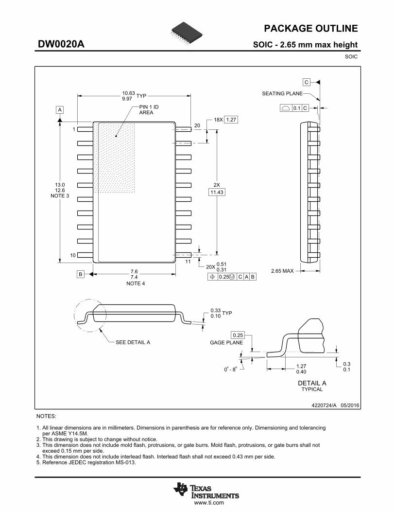
NFH0020A

www.ti.com
PACKAGE OUTLINE
C
TYP10.639.97
2.65 MAX
18X 1.27
20X 0.510.31
2X11.43
TYP0.330.10
0 - 80.30.1
0.25GAGE PLANE
1.270.40
A
NOTE 3
13.012.6
B 7.67.4
4220724/A 05/2016
SOIC - 2.65 mm max heightDW0020ASOIC
NOTES: 1. All linear dimensions are in millimeters. Dimensions in parenthesis are for reference only. Dimensioning and tolerancing per ASME Y14.5M. 2. This drawing is subject to change without notice. 3. This dimension does not include mold flash, protrusions, or gate burrs. Mold flash, protrusions, or gate burrs shall not exceed 0.15 mm per side. 4. This dimension does not include interlead flash. Interlead flash shall not exceed 0.43 mm per side.5. Reference JEDEC registration MS-013.
120
0.25 C A B
1110
PIN 1 IDAREA
NOTE 4
SEATING PLANE
0.1 C
SEE DETAIL A
DETAIL ATYPICAL
SCALE 1.200

www.ti.com
EXAMPLE BOARD LAYOUT
(9.3)
0.07 MAXALL AROUND
0.07 MINALL AROUND
20X (2)
20X (0.6)
18X (1.27)
(R )TYP
0.05
4220724/A 05/2016
SOIC - 2.65 mm max heightDW0020ASOIC
SYMM
SYMM
LAND PATTERN EXAMPLESCALE:6X
1
10 11
20
NOTES: (continued) 6. Publication IPC-7351 may have alternate designs. 7. Solder mask tolerances between and around signal pads can vary based on board fabrication site.
METALSOLDER MASKOPENING
NON SOLDER MASKDEFINED
SOLDER MASK DETAILS
SOLDER MASKOPENING
METAL UNDERSOLDER MASK
SOLDER MASKDEFINED

www.ti.com
EXAMPLE STENCIL DESIGN
(9.3)
18X (1.27)
20X (0.6)
20X (2)
4220724/A 05/2016
SOIC - 2.65 mm max heightDW0020ASOIC
NOTES: (continued) 8. Laser cutting apertures with trapezoidal walls and rounded corners may offer better paste release. IPC-7525 may have alternate design recommendations. 9. Board assembly site may have different recommendations for stencil design.
SYMM
SYMM
1
10 11
20
SOLDER PASTE EXAMPLEBASED ON 0.125 mm THICK STENCIL
SCALE:6X
www.ti.com
PACKAGE OUTLINE
C
TYP10.639.97
2.65 MAX
18X 1.27
20X 0.510.31
2X11.43
TYP0.330.10
0 - 80.30.1
0.25GAGE PLANE
1.270.40
A
NOTE 3
13.012.6
B 7.67.4
4220724/A 05/2016
SOIC - 2.65 mm max heightDW0020ASOIC
NOTES: 1. All linear dimensions are in millimeters. Dimensions in parenthesis are for reference only. Dimensioning and tolerancing per ASME Y14.5M. 2. This drawing is subject to change without notice. 3. This dimension does not include mold flash, protrusions, or gate burrs. Mold flash, protrusions, or gate burrs shall not exceed 0.15 mm per side. 4. This dimension does not include interlead flash. Interlead flash shall not exceed 0.43 mm per side.5. Reference JEDEC registration MS-013.
120
0.25 C A B
1110
PIN 1 IDAREA
NOTE 4
SEATING PLANE
0.1 C
SEE DETAIL A
DETAIL ATYPICAL
SCALE 1.200

www.ti.com
EXAMPLE BOARD LAYOUT
(9.3)
0.07 MAXALL AROUND
0.07 MINALL AROUND
20X (2)
20X (0.6)
18X (1.27)
(R )TYP
0.05
4220724/A 05/2016
SOIC - 2.65 mm max heightDW0020ASOIC
SYMM
SYMM
LAND PATTERN EXAMPLESCALE:6X
1
10 11
20
NOTES: (continued) 6. Publication IPC-7351 may have alternate designs. 7. Solder mask tolerances between and around signal pads can vary based on board fabrication site.
METALSOLDER MASKOPENING
NON SOLDER MASKDEFINED
SOLDER MASK DETAILS
SOLDER MASKOPENING
METAL UNDERSOLDER MASK
SOLDER MASKDEFINED

www.ti.com
EXAMPLE STENCIL DESIGN
(9.3)
18X (1.27)
20X (0.6)
20X (2)
4220724/A 05/2016
SOIC - 2.65 mm max heightDW0020ASOIC
NOTES: (continued) 8. Laser cutting apertures with trapezoidal walls and rounded corners may offer better paste release. IPC-7525 may have alternate design recommendations. 9. Board assembly site may have different recommendations for stencil design.
SYMM
SYMM
1
10 11
20
SOLDER PASTE EXAMPLEBASED ON 0.125 mm THICK STENCIL
SCALE:6X

IMPORTANT NOTICE
Texas Instruments Incorporated and its subsidiaries (TI) reserve the right to make corrections, enhancements, improvements and otherchanges to its semiconductor products and services per JESD46, latest issue, and to discontinue any product or service per JESD48, latestissue. Buyers should obtain the latest relevant information before placing orders and should verify that such information is current andcomplete. All semiconductor products (also referred to herein as “components”) are sold subject to TI’s terms and conditions of salesupplied at the time of order acknowledgment.TI warrants performance of its components to the specifications applicable at the time of sale, in accordance with the warranty in TI’s termsand conditions of sale of semiconductor products. Testing and other quality control techniques are used to the extent TI deems necessaryto support this warranty. Except where mandated by applicable law, testing of all parameters of each component is not necessarilyperformed.TI assumes no liability for applications assistance or the design of Buyers’ products. Buyers are responsible for their products andapplications using TI components. To minimize the risks associated with Buyers’ products and applications, Buyers should provideadequate design and operating safeguards.TI does not warrant or represent that any license, either express or implied, is granted under any patent right, copyright, mask work right, orother intellectual property right relating to any combination, machine, or process in which TI components or services are used. Informationpublished by TI regarding third-party products or services does not constitute a license to use such products or services or a warranty orendorsement thereof. Use of such information may require a license from a third party under the patents or other intellectual property of thethird party, or a license from TI under the patents or other intellectual property of TI.Reproduction of significant portions of TI information in TI data books or data sheets is permissible only if reproduction is without alterationand is accompanied by all associated warranties, conditions, limitations, and notices. TI is not responsible or liable for such altereddocumentation. Information of third parties may be subject to additional restrictions.Resale of TI components or services with statements different from or beyond the parameters stated by TI for that component or servicevoids all express and any implied warranties for the associated TI component or service and is an unfair and deceptive business practice.TI is not responsible or liable for any such statements.Buyer acknowledges and agrees that it is solely responsible for compliance with all legal, regulatory and safety-related requirementsconcerning its products, and any use of TI components in its applications, notwithstanding any applications-related information or supportthat may be provided by TI. Buyer represents and agrees that it has all the necessary expertise to create and implement safeguards whichanticipate dangerous consequences of failures, monitor failures and their consequences, lessen the likelihood of failures that might causeharm and take appropriate remedial actions. Buyer will fully indemnify TI and its representatives against any damages arising out of the useof any TI components in safety-critical applications.In some cases, TI components may be promoted specifically to facilitate safety-related applications. With such components, TI’s goal is tohelp enable customers to design and create their own end-product solutions that meet applicable functional safety standards andrequirements. Nonetheless, such components are subject to these terms.No TI components are authorized for use in FDA Class III (or similar life-critical medical equipment) unless authorized officers of the partieshave executed a special agreement specifically governing such use.Only those TI components which TI has specifically designated as military grade or “enhanced plastic” are designed and intended for use inmilitary/aerospace applications or environments. Buyer acknowledges and agrees that any military or aerospace use of TI componentswhich have not been so designated is solely at the Buyer's risk, and that Buyer is solely responsible for compliance with all legal andregulatory requirements in connection with such use.TI has specifically designated certain components as meeting ISO/TS16949 requirements, mainly for automotive use. In any case of use ofnon-designated products, TI will not be responsible for any failure to meet ISO/TS16949.
Products ApplicationsAudio www.ti.com/audio Automotive and Transportation www.ti.com/automotiveAmplifiers amplifier.ti.com Communications and Telecom www.ti.com/communicationsData Converters dataconverter.ti.com Computers and Peripherals www.ti.com/computersDLP® Products www.dlp.com Consumer Electronics www.ti.com/consumer-appsDSP dsp.ti.com Energy and Lighting www.ti.com/energyClocks and Timers www.ti.com/clocks Industrial www.ti.com/industrialInterface interface.ti.com Medical www.ti.com/medicalLogic logic.ti.com Security www.ti.com/securityPower Mgmt power.ti.com Space, Avionics and Defense www.ti.com/space-avionics-defenseMicrocontrollers microcontroller.ti.com Video and Imaging www.ti.com/videoRFID www.ti-rfid.comOMAP Applications Processors www.ti.com/omap TI E2E Community e2e.ti.comWireless Connectivity www.ti.com/wirelessconnectivity
Mailing Address: Texas Instruments, Post Office Box 655303, Dallas, Texas 75265Copyright © 2016, Texas Instruments Incorporated

Mouser Electronics
Authorized Distributor
Click to View Pricing, Inventory, Delivery & Lifecycle Information: Texas Instruments:
LM1036M LM1036M/NOPB LM1036MX LM1036MX/NOPB LM1036N LM1036N/NOPB