LLRF feedback control system (Basics) feedback control system (Basics) Feng QIU, JAS17, ......
103
LLRF feedback control system (Basics) Feng QIU, JAS17, Hayama, Kanagawa, Japan, 2017 1
-
Upload
trinhxuyen -
Category
Documents
-
view
223 -
download
0
Transcript of LLRF feedback control system (Basics) feedback control system (Basics) Feng QIU, JAS17, ......
LLRF feedback control system
(Basics)
Feng QIU, JAS17, Hayama, Kanagawa, Japan, 2017 1

RF & Accelerators Where is RF system (and LLRF system) in an accelerator?
I. The Radio Frequency (RF) systems in particle accelerators are the hardware
complexes devote to the generation of the accelerating field.
II. RF system :High Level RF (e.g. Klystron, waveguide, coupler…)+ control loops (LLRF).
Low Energy Beam High Energy Beam
RF System
Cav
LLRF
KlystronFeedBack
Beam
Target
RF system is very important in the accelerators!
Cavity
2Feng QIU, JAS17, Hayama, Kanagawa, Japan, 2017
I. Stabilizing the RF field
(field control)
II. Minimize the input power
(resonance control)

Feng QIU, JAS17, Hayama, Kanagawa, Japan, 2017 3
Introduction and Motivation

Introduction & Motivation
What is LLRF system?
Why we need LLRF feedback system?
Control theory (feedback and feedforward)
What is feedback and feedforward.
Transfer function and Bode plot.
Modeling of LLRF system
Cavity model and system model.
What will influence the performance of LLRF?
Whether the system is stable or not?
LLRF technology (will be talked by Prof. FANG in this school)
Field detection.
Field control and resonance control.
Examples
Main content
Feng QIU, JAS17, Hayama, Kanagawa, Japan, 2017 4

Feng QIU, JAS17, Hayama, Kanagawa, Japan, 2017 5
RF
Source Power
Supply
Master Oscillator
Pick-up
Waveguide
Beam
Crymodule
ADC
DAC DAC
Filed Detection
Feedback and Feedforward
Digital Signal Processing
Interlock
I/Q Modulator
Baseband
Clock
Distribution
Clock
Local Oscillator (LO)
RF
Pf
Pr
ADC ADC
Low-pass Filter
Intermediate Frequency (IF)
Pf Pr
Cavity
RF
Pre-amplifier
Cryogenic System Vacuum System
FPGAEPICSI
OC
Ethernet
Gate
Low level RF
HLRF & LLRF
High level RF
Cavity

Feng QIU, JAS17, Hayama, Kanagawa, Japan, 2017 6
RF
Source Power
Supply
Master Oscillator
Pick-up
Waveguide
Beam
Crymodule
ADC
DAC DAC
Filed Detection
Feedback and Feedforward
Digital Signal Processing
Interlock
I/Q Modulator
Baseband
Clock
Distribution
Clock
Local Oscillator (LO)
RF
Pf
Pr
ADC ADC
Low-pass Filter
Intermediate Frequency (IF)
Pf Pr
Cavity
RF
Pre-amplifier
Cryogenic System Vacuum System
FPGAEPICSI
OC
Ethernet
Gate
ADC: LTC 2208
Xillinx Virtex5 FPGA
ADC & DAC Interface
Digital I/O
uTCA Digital Board
HLRF & LLRF
Digital Board
Cavity
Klystron
Waveguide

Feng QIU, JAS17, Hayama, Kanagawa, Japan, 2017 7
Why LLRF?
We have lots of disturbances…
I. High voltage power supply
ripples
II. Lorentz detuning
III. Beam-loading
IV. Microphonics
V. Phase noise of MO
VI. Drift of temperature and
humidity
RF
Source Power
Supply
Master Oscillator
Pick-up
Waveguide
Beam Loading
Crymodule
ADC
DAC DAC
I/Q Modulator
Baseband
Clock
Distribution
Clock
Local Oscillator (LO)
RF
Pf
Pr
ADC ADC
Low-pass Filter
Intermediate Frequency (IF)
Pf Pr
Cavity
RF
Pre-amplifier
Ripples
Cryogenic System Vacuum System
Microphonics
Ethernet
LFD Effects
Filed Detection
Feedback and Feedforward
Digital Signal Processing
Interlock
FPGAEPICSI
OCGate

Feng QIU, JAS17, Hayama, Kanagawa, Japan, 2017 8
Examples (PS Ripples)
We have lots of disturbances…
I. High voltage power supply
ripples
II. Lorentz detuning
III. Beam-loading
IV. Microphonics
V. Phase noise of MO
VI. Drift of temperature and
humidity
RF
Source Power
Supply
Master Oscillator
Cavity Signal
Waveguide
Beam Loading
Crymodule
ADC
DAC DAC
I/Q Modulator
Baseband
Clock
Distribution
Clock
Local Oscillator (LO)
RF
Pf
Pr
ADC ADC
Low-pass Filter
Intermediate Frequency (IF)
Pf Pr
Cavity
RF
Pre-amplifier
Ripples
Cryogenic System Vacuum System
Microphonics
Ethernet
LFD Effects
Filed Detection
Feedback and Feedforward
Digital Signal Processing
Interlock
FPGAEPICSI
OCGate
Disturbances
Vc
Feng QIU, JAS17, Hayama, Kanagawa, Japan, 2017 9
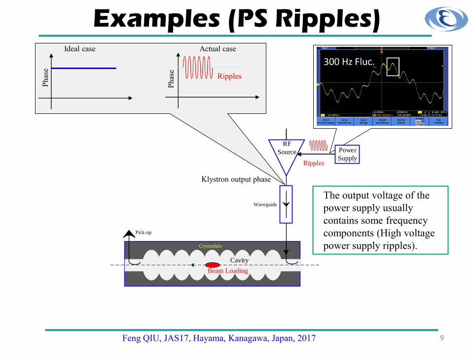
Examples (PS Ripples)
RF
Source Power
Supply
Pick-up
Waveguide
Beam Loading
Crymodule
Cavity
Ripples
Ripples
Actual caseIdeal case
Klystron output phase
Phas
e
Phas
e
The output voltage of the
power supply usually
contains some frequency
components (High voltage
power supply ripples).

RF
Source Power
Supply
Pick-up
Waveguide
Beam Loading
Crymodule
Cavity
Ripples
cV t
Feng QIU, JAS17, Hayama, Kanagawa, Japan, 2017 10
Examples (PS Ripples)
Klystron output phase
Spectrum of Cavity Voltage

Pick-up
Beam Loading
Crymodule
Cavity
cV t
Feng QIU, JAS17, Hayama, Kanagawa, Japan, 2017 11
Why LLRF?
Amp
Phase
W/O LLRF (not “flat”) With LLRF (“flat” voltage)
cV t
cV t
cV t
cV t
Not flat
We want them flat
We need a “flat” cavity voltage for beam accelerating.
Phase Stability
Requirement of RF system
E.g.: ΔA/A<0.1% rms,
Δθ<0.1 deg. rms
θ
Amplitude StabilityAΔA
Δθ

12
Amp
CW (Continuous Wave) mode (Continuous RF field), all the time there is RF.
Pulsed Mode: Only amount of time is used for beam acceleration.
Pulse mode and CW mode
International Linear Collider (ILC)
Amp RF pulseCW

Feng QIU, JAS17, Hayama, Kanagawa, Japan, 2017 13
Control Theory

What is a control system? A control system is a device, or set of devices, that manages, commands,
directs or regulates the behavior of other devices or systems. Industrial control
system are used in industrial production for controlling equipment or machines.
(Definition from Wikipedia).
A control system mainly include a plant, a sensor and a controller.
Requirements: maintain some characteristics or behavior of the “plant”.
Systems or
devices that need
to be controlled
A device that regulate or control the
behavior of the “Plant”
14Feng QIU, JAS17, Hayama, Kanagawa, Japan, 2017
Measuring tool that measured
the response of the “Plant”
PlantController
Sensor

PlantController
Sensor
Main components (Examples)
Plant: Cavities, power source,
RF Gun, antenna,…
Sensor: Phase detector,
amplitude discriminator,
or FPGA
Controller: Electrical control
phase shifter or attenuator,
FPGA
ADC: LTC 2208
Xillinx Virtex5 FPGA
ADC & DAC Interface
Digital I/O
uTCA Digital Board
Cavity
Examples: Digital low-level RF system.
The field-programmable-gate-array (FPGA) plays roles of both controller and
sensor (core component, will be introduced later).
Requirements: making the RF field inside the cavity stable (most significant
goal).
FPGA
15
Target: Stabilize
the field inside
the cavity
Feng QIU, JAS17, Hayama, Kanagawa, Japan, 2017

Close Loop vs. Open loop Open loop control systems vs. closed loop control systems.
In open loop control systems output is generated based on feedforward (FF).
In close loop control systems current output is taken into consideration and
corrections are made based on feedback. A closed loop system is also called a
feedback (FB) control system (from wiki).
To analyze how does a FB control system works, let’s start from “Transfer
function”.
PlantFF
Sensor
PlantFB
Controller
Sensor
Reference
Close loop Open loop
Open loop Closed loop
Advantages Generally stable
Easier construction Good disturbances rejection
Disadvantages Poor disturbances rejection Unstable risk
Difficult construction 16
Feedback

Transfer function A Transfer Function (TF) is the ratio of the output of a system to the input of
a system.
The X(s) and Y(s) are the Laplace-transform of the input/output signal,
respectively.
Key point: The transfer function H(s) includes every information of the
system (usually can be seen as a representation of a system model). i.e. if
we know the transfer function H(s) of a specified system, we can calculate the
output Y(s) by any input X(s).
System
Y(s)
X(s)
, .
Y sH s Y s H s X s
X s
Time domain
Complex freq.
domain
Freq. domain
h t
H s
H j
Laplace-transform
Fourier-transform
Transfer function
17Feng QIU, JAS17, Hayama, Kanagawa, Japan, 2017

TF & Frequency response Frequency response It is a measure of magnitude and phase of the output as a
function of frequency.
From TF to transfer function: H(s)→H(jω).
Key point: Direct magnitude (amplitude) and phase response for a specified
sinusoidal input.
H(s)
Y(s)
X(s)
j H j
s jH s H j H j e
: sin 2 50 ,
: sin 2 50
If input t
Then output H j t H j
E.g. a 50 Hz sinewave
Magnitude gain Phase delayStill 50 Hz, but,…
18
20 ms 20 ms
Feng QIU, JAS17, Hayama, Kanagawa, Japan, 2017

Examples: H(s) & H(jω)
Cavity transfer function
1
sC
Ls
R
2
2
1 1 1
1 1
s
Ls RLCs R CsC Z sZ R Ls RLs
s sRC LC
0
02 2 2 20
0 0
1,
1
Rs sC QCQ R Z sL LC
s s s sRC Q
Quality factor or Q value
Resonance radian frequency
1C
L
XsC
X Ls
19

Examples: H(s) & H(jω) cnt’d
Cavity transfer function
1
sC
Ls
R
0 0 0
22 2 2 2 2 20 0 0 0
0 0 0
1
Rs s j R j RQ Q QCZ s Z j
s s s s j jRC Q Q Q
0 , , ,if then Z j R cavity is on resonance
Resonance radian frequency
1C
L
XsC
X Ls
Feng QIU, JAS17, Hayama, Kanagawa, Japan, 2017 20

Bode Plot
Bode diagram ( Plots of the amplitude-frequency and phase-frequency
response of the system)
0
2 2 2 200 0
1
Rs sQCZ s
s s s sRC Q
9
0 0
6
. . 2 2 1.3 10 [ / ]
1.3 10
E g f rad s
Q
Bode Plot
• Magnitude vs. frequency
• Phase vs. frequency
• Matlab function: bode(sys)
21
Z j
Z j
Z(s)
Y(s)
X(s)

Bode plot (cont’d)
Bode Plot (Example1)
• 𝜔0 = 1.3 ∙ 2𝜋 [𝑟𝑎𝑑/𝑠]• 𝑄 = 1.3 × 10⁶
Bode Plot (Example2)
• 𝜔0 = 1.3 ∙ 2𝜋 [𝑟𝑎𝑑/𝑠]• 𝑄 = 7000
• The half power point of an electronic
amplifier stage is that frequency at which
the output power (not voltage) has dropped
to half of its mid-band value. That is a level
of -3 dB.
• 3-dB Bandwidth (BW):
• Example1: BW1=100 [Hz], Example2:
BW2=186 [kHz]
-3 dBBandwidth
Bandwidth
𝑓1𝑓2
𝑓2 − 𝑓1
22
90 deg.
90 deg.

Bode plot (cont’d)Bode Plot (Example1)
• 𝜔0 = 1.3 × 10⁹ ∙ 2𝜋 [𝑟𝑎𝑑/𝑠]• 𝑄1 = 1.3 × 10⁶
• 𝐵𝑊1 = 100 [𝐻𝑧]
Bode Plot (Example2)
• 𝜔0 = 1.3 × 10⁹ ∙ 2𝜋 [𝑟𝑎𝑑/𝑠]• 𝑄2 = 7000• 𝐵𝑊2 = 186000 [𝐻𝑧]
0 03 0,
2dB
fBW f
Q
𝐵𝑊1 = 100 [𝐻𝑧]
𝐵𝑊2 = 186000 [𝐻𝑧]
𝑄2 = 7000𝑄1 = 1.3 × 10⁶
Resonance frequency
23
𝐶𝑎𝑠𝑒1
𝐶𝑎𝑠𝑒2
𝑍𝑜𝑜𝑚
𝐵𝑊1
SC cavity NC cavity
Case1
Case2

Feng QIU, JAS17, Hayama, Kanagawa, Japan, 2017 24
Modeling (TF) of LLRF system
Cavity Model
25
Cavity is like a parallel resonance circuit.
Detuning:
1
sC
Ls
R
1C
L
XsC
X Ls
frequency
2H j f
0
RF
RF
0
2 200
RF
Rs
QP s
s sQ
Band-pass Filter
dt
dIRV
dt
dV
dt
VdLc
cc2/1
2
02/12
2
22
0
0.5
TFDiff. equation
0 RF

RF vs. Baseband
i t
c cV V e cV
2
RF
dt
dIRV
dt
dV
dt
VdLc
cc2/1
2
02/12
2
22
0.5 0.5c
c
dVj V u
dt
RFj t
e
NOT interesting, We do not care
We are interested in the
base band (envelope).
LLRF directly regulate the
base-band.
Feng QIU, JAS17, Hayama, Kanagawa, Japan, 2017
First order
Second order
33
0 RF

Cavity Model (RF to Baseband)
27
In the frequency domain.
1
sC
Ls
R
1C
L
XsC
X Ls
frequency
2H j f
0
If detuning exist
0
2 200
RF
Rs
QP s
s sQ
0.5
0.5
c
cav
V sP s
U s s j
0.5 0.5
cc
dVj V u
dt
RF ( )Baseband (0 Hz)
0
t
RF
RF

Cavity Model (detuning=0)
28
If there is no detuning, we have the simplified cavity model.
1
sC
Ls
R
1C
L
XsC
X Ls
frequency
2H j f
0 1.3RFf GHz
0
2 200
RF
Rs
QP s
s sQ
0.5
0.5
baseP ss
If detuning=0
Low-pass Filter
Band-pass Filter
0 RF
0
RFbaseband

PI controller PI control is very popular in the FB control system (& LLRF FB control system)
PI Controller
1 I
P
Y s KK s K
E s s
Feng QIU, JAS17, Hayama, Kanagawa, Japan, 2017 29
e tPK
IK
y t PK e t
P P Iy t K e t K K e t dt
P P I
E sY s K E s K K
s
Lapalce Transform
F sf t dt
s
ADC: LTC 2208
Xillinx Virtex5 FPGA
ADC & DAC Interface
Digital I/O
uTCA Digital Board
Usually performed in
the FPGA (or DSP)
1/ s

Sensor (IQ detector)
Feng QIU, JAS17, Hayama, Kanagawa, Japan, 2017 30
ADC: LTC 2208
Xillinx Virtex5 FPGA
ADC & DAC Interface
Digital I/O
uTCA Digital Board
Usually performed in
the FPGA (or DSP)
F
F
F ss
0.5F
Cavity half bandwidth
low pass filter
detector -3dB bandwidth
Detector can be also seen as a low pass filter but with higher bandwidth
than cavity.

Analytical Study (components) Basically, we have all of the LLRF components.
F
F
F ss
31
1 IP
KK s K
s
PlantController
Sensor
0.5
0.5
0baseP ss
Feng QIU, JAS17, Hayama, Kanagawa, Japan, 2017
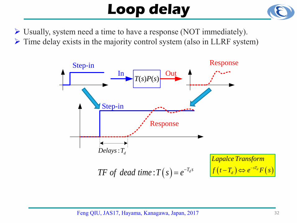
Loop delay
Usually, system need a time to have a response (NOT immediately).
Time delay exists in the majority control system (also in LLRF system)
T(s)P(s)In Out
Step-in Response
Step-in
Response
: dT sTF of dead time T s e
: dDelays T
Feng QIU, JAS17, Hayama, Kanagawa, Japan, 2017 32
dsT
d
Lapalce Transform
f t T e F s

Analytical Study (components) Now, we insert the loop delay in the system.
F
F
F ss
33
1 IP
KK s K
s
PlantController
Sensor
0.5
0.5
0baseP ss
Feng QIU, JAS17, Hayama, Kanagawa, Japan, 2017
dT sT s e
Delay

TF of overall LLRF Now, the overall model can be constructed.
But, how to obtain the transfer function of the overall system?
Reference
Closed loop
IP
KK
s 0.5
0.5s
F
Fs
dT s
e
Reference
Open loop
IP
KK
s 0.5
0.5s
F
Fs
Disconnected
dT se
r
yr
Feng QIU, JAS17, Hayama, Kanagawa, Japan, 2017 34
1 IP
KK
s
1 I
P
KK
s
Controller
Loop Delay
Plant (cavity)
Sensor

Block diagram transformations How to calculate the TF of the whole system if we know the TF of each
subsystem?
35
1G s 1G s 2 1G s G s
1G s
1G s
1G s
2G s
1 2G s G s
1
2 11
G s
G s G s
X s Y s
X s Y s
Y s X s
2 1
Y sG s G s
X s
1 2
Y sG s G s
X s
1
2 11
Y s G s
X s G s G s
Minus
Serial
Parallel
Feedback

TF of overall LLRF Now, the overall model can be constructed.
Over all TF (open loop).
Reference
Closed loop
IP
KK
s 0.5
0.5s
F
Fs
dT s
e
Reference
Open loop
IP
KK
s 0.5
0.5s
F
Fs
Disconnected
dT se
Feng QIU, JAS17, Hayama, Kanagawa, Japan, 2017 36
1 IP
KK
s
1 I
P
KK
s
0.5
0.5
dT sI P P Floop
F
K K K sH s e
s s s
1G s 1G s 2 1G s G s X s Y s

TF of disturbances to cavity output
We are interesting with the TF from disturbances to cavity voltage (most
significant)?
Reference
Closed loop
IP
KK
s 0.5
0.5s
F
Fs
dT s
e
Reference
Open loop
IP
KK
s 0.5
0.5s
F
Fs
Disconnected
dT se
y
r
Feng QIU, JAS17, Hayama, Kanagawa, Japan, 2017 37
1 IP
KK
s
1 I
P
KK
s
Disturbances Disturbances
Cavity
outputCavity
output
d
y
dy
1G s
2G s
1
2 11
G s
G s G s Y s D s
0.5
0.5
dT sI P P Floop
F
K K K sH s e
s s s
1
1CL
loop
G sH s d y
H s

TF of disturbances to cavity output
How about the TF from disturbances to cavity voltage (most significant)?
Reference
Closed loop
IP
KK
s
F
Fs
dT s
e
Reference
Open loop
IP
KK
s 0.5
0.5s
F
Fs
Disconnected
dT se
0.5
0.5s
y
r
Feng QIU, JAS17, Hayama, Kanagawa, Japan, 2017 38
1 IP
KK
s
1 I
P
KK
s
Disturbances
Cavity
output
d
y
dy
1G s
2G s
1
2 11
G s
G s G s Y s D s
0.5
0.5
dT sI P P Floop
F
K K K sH s e
s s s
2G s
0.5
0.5
1CL
loop
sH s d y
H s

TF of disturbances to cavity output
How about the TF from disturbances to cavity voltage (most significant)?
Reference
Closed loop
IP
KK
s 0.5
0.5s
F
Fs
dT s
e
Reference
Open loop
IP
KK
s 0.5
0.5s
F
Fs
Disconnected
dT se
0.5
0.5
1CL
loop
sH s d y
H s
Feng QIU, JAS17, Hayama, Kanagawa, Japan, 2017 39
1 IP
KK
s
1 I
P
KK
s
0.5
0.5
OLH s d ys
Disturbances Disturbances
Cavity
outputCavity
output
d
y
dy
1G s
2G s Y s D s
1G s
Y s D s

RF
Source Power
Supply
Pick-up
Waveguide
Beam Loading
Crymodule
Cavity
Ripples
RF
Source Power
Supply
Pick-up
Waveguide
Beam Loading
Crymodule
Cavity
Ripples
cV t
Feng QIU, JAS17, Hayama, Kanagawa, Japan, 2017 40
TF of disturbances to cavity output
F
Fs
1
IP
KK
s
cV ty
d
y
d
Closed loop Open loop
0.5
0.5s
0.5
0.5s
0.5
0.5
1CL
loop
sH s d y
H s
0.5
0.5
OLH s d ys
-
1G s
2G s Y s D s 1G s
Y s D s

Effects of the loop gain Let’s observe the frequency response.
41
1
101
1
11
1
2
1
, 0
, 0
10
1
1
CL d y loop P
P
OL d y
H j H KK
H j
0.5
0.5
0dT s Floop P I
F
H s K e Ks s
Low
KP
High
KP
0.5
0.5
1CL
loop
sH s d y
H s
0.5
0.5
OLH s d ys
OLH

TF & Frequency response Frequency response It is a measure of magnitude and phase of the output as a
function of frequency.
From TF to transfer function: H(s)→H(jω).
Key point: Direct magnitude (amplitude) and phase response for a specified
sinusoidal input.
H(s)
Y(s)
X(s)
j H j
s jH s H j H j e
: sin 2 50 ,
: sin 2 50
If input t
Then output H j t H j
E.g. a 50 Hz sinewave
Magnitude gain Phase shiftStill 50 Hz, but,…
42
20 ms 20 ms

RF
Source Power
Supply
Pick-up
Waveguide
Beam Loading
Crymodule
Cavity
Ripples
Feng QIU, JAS17, Hayama, Kanagawa, Japan, 2017 43
TF of disturbances to cavity output
F
Fs
PK
cV ty
d
0.5
0.5s
LLRF-
0
1 10
1d y loop P
P P
H j H KK K
d yH s
d yH s
d yH s
d yH s
d yH s
Open loop
KP=1
How about KP = ∞?
KP=10
KP=100
KP=∞
KP=0
KP=1000
PS ripples (d) Vc (y)

Stability Criteria Stable is one of the most important thesis in a feedback system, if
the system is not stable, there is no meaning for any efforts.
The Stability Criteria for a feedback system includes
1. Root locus
2. Solve the characteristic equation
3. Open loop bode plot
4. Routh–Hurwitz stability criterion
All of them are important, but…
Bode plot is the most simple one in our case, it provide not only a
stability criteria but also a simple way to observe the important
specifications of a system.
Stability criteria
Open loop-based Closed loop-based
Root locus Bode plot Characteristic equation Routh–Hurwitz
44Feng QIU, JAS17, Hayama, Kanagawa, Japan, 2017

Stability Criteria Definition: A stable system is a dynamic system with a bounded
response to a bounded input.
Feng QIU, JAS17, Hayama, Kanagawa, Japan, 2017 45
X(s)
Y(s)
H s
1 2
1 2 1 0
1 2
1 2 1 0min
m m m
m m m
n n n
n n
b s b s b s b s bnumeratorH s
deno ator s a s a s a s a
Characteristic equation
bounded inputStable
Unstable
We can not try all of the bounded input signal anyway
time time
x(t) y(t)

Stability Criteria (bode plot)
Feng QIU, JAS17, Hayama, Kanagawa, Japan, 2017 46
frequency
frequency
1020log 2H j f
2H j f
dB
degree
f
f
-180 deg
180f
1802 1H j f G(s): Stable
crossf
0 dB
180 deg
PlantFF
Sensor
Open loop
Find the frequency where the PHASE becomes -180 degrees (@ lower plot).
Find the GAIN, G (in dB), at this SAME FREQUENCY (@ upper plot).
If the value of G less than 0 dB, then system is STABLE, or, system is
UNSTABLE.
If time delay is 0
time delay ≠ 0 (actual case)

Stability Criteria (bode plot)
Feng QIU, JAS17, Hayama, Kanagawa, Japan, 2017 47
frequency
frequency
1020log 2H j f
2H j f
dB
degree
f
f
-180 deg
180f
1802 1H j f G(s): Stable
crossf
0 dB
180 deg
10 1800 20log 2G j f
180 2 crossG j f
Larger margin→ Better robustnessGain Margin:
Phase Margin
Gain margin
Phase margin

Effects of the loop gain If gain is too large, system may be unstable.
0.51 0
0.5
dT s FOL
F
H s K es s
frequency
frequency
1020log 2H j f
2H j f
dB
degreef
f
-180 deg
180f
Stable
crossf
0 dB
180 deg
0.52 0
0.5
10 dT s FOL
F
H s K es s
1 2OL OLH j H j
Phase margin
1OLH j
2OLH j20 dB
Feng QIU, JAS17, Hayama, Kanagawa, Japan, 2017 48
Unstable
Gain margin
d yH s
1,2OLH

Feng QIU, JAS17, Hayama, Kanagawa, Japan, 2017 49
Digital LLRF System

LLRF System (Review)
PlantController
Sensor
ADC: LTC 2208
Xillinx Virtex5 FPGA
ADC & DAC Interface
Digital I/O
uTCA Digital Board
Cavity
FPGA
Controller: Electrical control
phase shifter or attenuator,
FPGA
Sensor: Phase detector,
amplitude discriminator,
or FPGA
50Feng QIU, JAS17, Hayama, Kanagawa, Japan, 2017

Digital LLRF Digital LLRF is the current tendency.
Both the sensor and controller are performed by FPGA (digital
devices)
PlantController
Sensor
ADC: LTC 2208
Xillinx Virtex5 FPGA
ADC & DAC Interface
Digital I/O
uTCA Digital Board
Cavity
FPGA
DAC
ADC
Controller: Electrical control
phase shifter or attenuator,
FPGA
Sensor: Phase detector,
amplitude discriminator,
or FPGA
51
:SF Sampling
SF
Feng QIU, JAS17, Hayama, Kanagawa, Japan, 2017

Z-transform Very similar with Laplace transform.
h t
H s
0
st
tH s h t e dt
Z-domainS-domain
kH z h k z
h k
sk n Th k h t
Impulse response
H z
Discrete time
Laplace-transform z-transform
Feng QIU, JAS17, Hayama, Kanagawa, Japan, 2017 52
sk n T
f k f t
f t
ST

Feng QIU, JAS17, Hayama, Kanagawa, Japan, 2017 53
LLRF technology

Field and Resonance control
Feng QIU, JAS17, Hayama, Kanagawa, Japan, 2017 54
Tuner(frequency
ctrl.)FB
(field ctrl.)
Piezo
Kly/SSACavity
Pf
Pick up
Pf
Pick up
Pick up
Internet
Communication
PC
Two main feedback loops in the LLRF.

Field and Resonance control
Feng QIU, JAS17, Hayama, Kanagawa, Japan, 2017 55
Tuner(frequency
ctrl.)FB
(field ctrl.)
Piezo
Kly/SSACavity
Pf
Pick up
Pf
Pick up
Pick up
Internet
Communication
PC
2H j f
t
Optimize the detuning tominimize the klystron power
0.5 0.5c
c
dVj V u
dt

Field and Resonance control
Feng QIU, JAS17, Hayama, Kanagawa, Japan, 2017 56
Tuner(frequency
ctrl.)FB
(field ctrl.)
Piezo
Kly/SSACavity
Pf
Pick up
Pf
Pick up
Pick up
Internet
Communication
PC
cA V
cP V
Stabilize the RF field (A&P) for beam acceleration
2H j f
t
Minimize the klystron power
0.5 0.5c
c
dVj V u
dt
“Flat”

Feng QIU, JAS17, Hayama, Kanagawa, Japan, 2017 57
PlantController
Sensor
ADC: LTC 2208
Xillinx Virtex5 FPGA
ADC & DAC Interface
Digital I/O
uTCA Digital Board
Cavity
FPGA
Field and Resonance control
PlantController
Sensor
ADC: LTC 2208
Xillinx Virtex5 FPGA
ADC & DAC Interface
Digital I/O
uTCA Digital Board
Tuner & Cavity
FPGA
Frequency
Control
Field Control
cSet V
Set
Feng QIU, JAS17, Hayama, Kanagawa, Japan, 2017 58
Field Detection
Field Detection
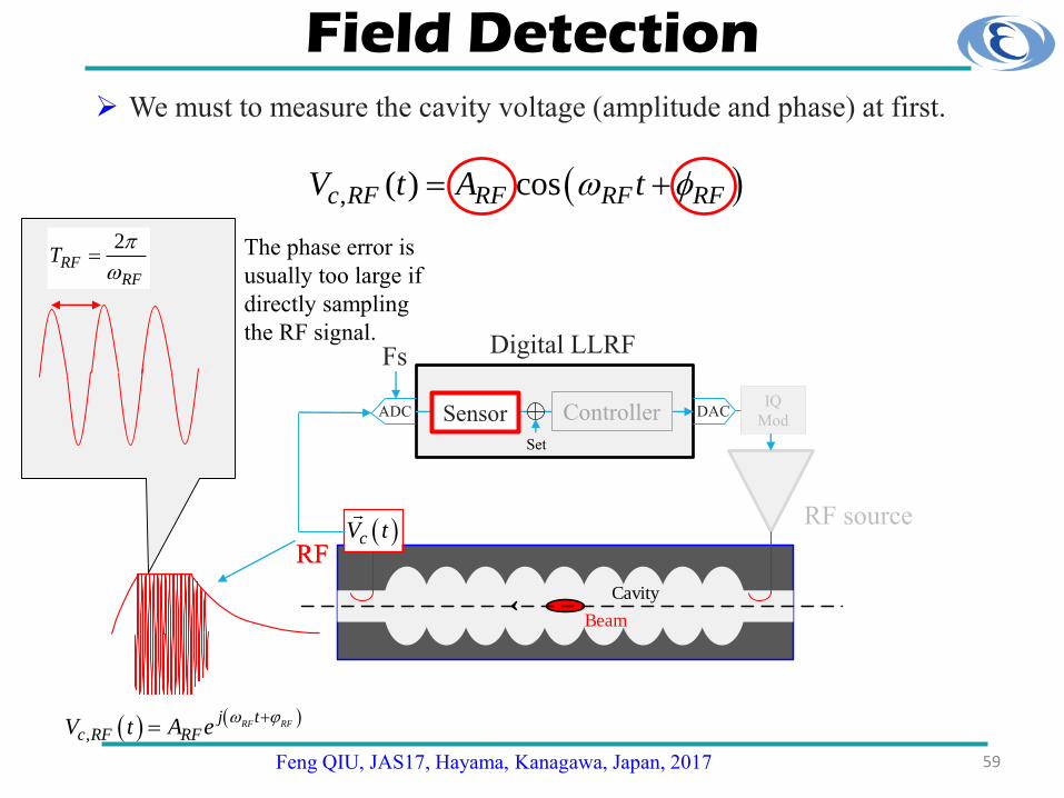
Feng QIU, JAS17, Hayama, Kanagawa, Japan, 2017 59
We must to measure the cavity voltage (amplitude and phase) at first.
, ( ) cosc RF RF RF RFV t A t
Beam
Cavity
cV tRF source
ControllerSensor
RF
Digital LLRF
ADC DAC
2RF
RF
T
Set
RF
,
RF RFj t
c RF RFV t A e
IQ
Mod
The phase error is
usually too large if
directly sampling
the RF signal.Fs

Field Detection
60
Usually, it is difficult to process the RF signal directly.
Beam
Cavity
cV tRF source
ControllerSensor
RF
Digital LLRF
ADC DAC
LO
IF
,
RF RFj t
c RF RFV t A e
,
IF RFj t
c IF RFV t A e
, 2 LO
j tc LOV t e
cos 2cos cos cosmixer RF RF RF LO RF IF RF RF LO RFV A t t A t t t
Filtered by LPF
LO RF IF
Set
Feng QIU, JAS17, Hayama, Kanagawa, Japan, 2017
IQ
Mod
Fs

Field Detection
61
Finally, we need to demodulate the baseband signal (A & φ) in the
FPGA.
Beam
Cavity
cV tRF source
ControllerSensor
RF
Digital LLRF
ADC DAC
LO
IF
, 2 LO
j tc LOV t e
LO RF IF
Set
,RF
jc base RFV t A e
Fs
,
RF RFj t
c RF RFV t A e
,
IF RFj t
c IF RFV t A e
Feng QIU, JAS17, Hayama, Kanagawa, Japan, 2017
IQ
Mod

How to get the baseband
I Q
-I -Q
Time [s]
IQ S
amp
ling:
2 2
cos.
sin
.arctan
RF RF
RF RF
RF
RF
I A
Q A
A I Q
Q I
Usually, it is more convenient to demodulate the in-phase (I) and quadrature
(Q) signal.
Simplest way: IQ sampling.
Controller
IQ dem.
Digital LLRF
ADC
DACIF
Controller DAC
I
Q
Fs
1
4
IF
s
f
F
64
Sensor
Set

Non-IQ
Nonlinearities in the analog front-end or the ADC generate harmonics, which will be aliased to the IF frequency.
Non-IQ sampling (higher precision).
Perfect
Real
4
15
IF
s
f M
F N 2
M
N
Feng QIU, JAS17, Hayama, Kanagawa, Japan, 2017 63
f k

IQ dem.
Non-IQ The demodulation algorithm is derived from the Fourier series.
1
0
1
0
cos
2cos 2 ,
2sin 2 .
SRF IF RF t k T
n
k
n
k
f k A t
MI f k k
N N
MQ f k k
N N
₁ z ₁ z +
CosSin
₁ z
...
₁ z
₁ z + ₁ z
...
IF
I
Q
Feng QIU, JAS17, Hayama, Kanagawa, Japan, 2017 64
Controller
Digital LLRF
ADC
DACIF
Controller DAC
I
Q
Fs
Sensor
Set

Up Conversion Recover the RF signal with IQ modulator.
Controller
IQ dem.
Digital LLRF
ADC
DACIF
Controller DAC
I
QFs
Feng QIU, JAS17, Hayama, Kanagawa, Japan, 2017 65
2 2 1
cos sin cos
, tan
RF RF RFOut I t Q t A t
QA I Q
I
90
RF
I
QIQ
Modulator
RF source
I
Q
RF
OUT-
To cavity

Feng QIU, JAS17, Hayama, Kanagawa, Japan, 2017 66
Field Control
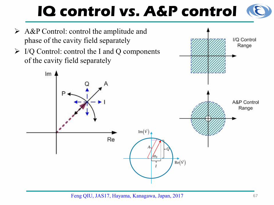
IQ control vs. A&P control
Feng QIU, JAS17, Hayama, Kanagawa, Japan, 2017 67
A&P Control: control the amplitude and
phase of the cavity field separately
I/Q Control: control the I and Q components
of the cavity field separately
0
I
QA
Re V
Im V

IQ control vs. A&P control
Feng QIU, JAS17, Hayama, Kanagawa, Japan, 2017 68
• I/Q control
– Set point can cover the four quadrants including zero
– Good for the control of large errors and large beam loading
– Coupling between I/Q channels if the loop phase is wrong
• A&P control
– No loop phase problem
– If there is large phase error, the cavity output may be driven to wrong
quadrants

Closed loop
dT s
e
K(s) P(s)
F(s)
d(t)
n(t)
w(t)
y(t)
r(t)
TF of LLRF system
dT s
olH s K s P s e F s
1d y
ol
Y s P sH
D s H s
1n y
ol
N s F s K s P sH
D s H s
Transfer function of disturbances
d(t) to cavity output y(t)
Transfer function of disturbances
n(t) to cavity output y(t)
Feng QIU, JAS17, Hayama, Kanagawa, Japan, 2017 69
1r y
ol
K s P sH s
H

Disturbance and Noise Transfer
Parameters for the bode plot:
• Cavity detuning = 0
• Half bandwidth = 217 Hz
• Loop gain = 100
• Detector bandwidth = 500 kHz
Conclusion:
• Low frequency disturbances are
suppressed by feedback gain
(~40 dB)
• FB gain only suppress d(t), not
n(t).
• Reducing the detector noise n(t)
will be essential to get highly
stable cavity field!
1
100
Feng QIU, JAS17, Hayama, Kanagawa, Japan, 2017 70
d yH
n yH
Increase
Gain

Cavity
71
TF of disturbances to cavity output
d yH s
d yH s
d yH s
d yH s
Open loop
KP=1
KP=10
KP=100
KP=0
PS ripples Vc
n yH s
n yH s
n yH s
n yH s
Open loop
Noise Vc
cV t
KPSensorADC DAC
LO
Noise (n)
LO RF IF
Set
IQ
Mod
Ripples (d)

Suppression of Microphonics
The measurement of Microphnics at KEK cERL.
No Feedback (Gain=0)
Gain ≈ 10
Gain ≈ 150
Closed loop
dT s
e
K(s) P(s)
F(s)
d(t)
n(t)
w(t)
y(t)
r(t)
FFT of Microphonics
72
Gain
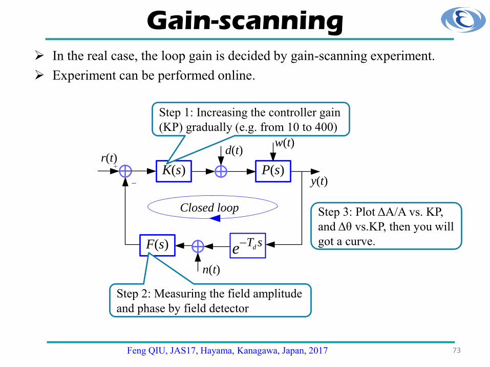
Gain-scanning In the real case, the loop gain is decided by gain-scanning experiment.
Experiment can be performed online.
Closed loop
dT s
e
K(s) P(s)
F(s)
d(t)
n(t)
w(t)
y(t)
r(t)
Step 1: Increasing the controller gain
(KP) gradually (e.g. from 10 to 400)
Step 2: Measuring the field amplitude
and phase by field detector
Step 3: Plot ΔA/A vs. KP,
and Δθ vs.KP, then you will
got a curve.
Feng QIU, JAS17, Hayama, Kanagawa, Japan, 2017 73

Effects of the loop gain If gain is too large, system may be unstable.
0.51 0
0.5
dT s FOL
F
H s K es s
frequency
frequency
1020log 2H j f
2H j f
dB
degreef
f
-180 deg
180f
Stable
crossf
0 dB
180 deg
0.52 0
0.5
10 dT s FOL
F
H s K es s
1 2OL OLH j H j
Phase margin
1OLH j
2OLH j20 dB
Feng QIU, JAS17, Hayama, Kanagawa, Japan, 2017 74
Unstable
Gain margin
d yH s
1,2OLH

I gain is set to be zero, optimum P gain is about 125.
Gain Scanning @ KEK cERL
KI=0
Feng QIU, JAS17, Hayama, Kanagawa, Japan, 2017 75

Gain-scan with integral gain
P Gain
I G
ain
Measured
Performance
O Pmax
Imax
I=0
Two-D Mapping
P Gain
I G
ain
Optimized
Gains
Bad
Good
Imax
O
e tPK
IK
y t PK e t
Integral gain
Sometimes we are also interested in the integral gain, KI, which is
significant in the normal conducting cavity LLRF (think about why?).
We will get an 2-D map in this case if we scan both KP and KI.
I=10
Feng QIU, JAS17, Hayama, Kanagawa, Japan, 2017 76

Feng QIU, JAS17, Hayama, Kanagawa, Japan, 2017 77
Resonance Control

Resonance control
78
Tuner(frequency
ctrl.)FB
(field ctrl.)
Piezo
Kly/SSACavity
Pf
Pt
Pf
Pt
Pt
Internet
Communication
PC
cA V
cP V
Stabilize the RF field (A&P) for beam acceleration
2H j f
t
Minimize the cavity input power
related to t
0.5 0.5c
c
dVj V u
dt
Feng QIU, JAS17, Hayama, Kanagawa, Japan, 2017

Main Detuning
79
2H j f
0
t
RF
Cavity
Deformation
of the cavity
Repulsive
magnetic force
Attractive
Electric force
MicrophonicsLorentz detuning
Lorentz detuning: usually effects
the PS mode machine.
Microphonics: effects both of
pulse mode and CW mode.
It is difficult to apply the FB
control for Lorentz detuning (in
PS mode), feedforward is
recommended (think about
why?).
Feng QIU, JAS17, Hayama, Kanagawa, Japan, 2017

Tuner control
Tuner system is used to compensate the cavity detuning.
80∆𝑓: detuning
H(s): Desired case
freq
Detuning effect
Lorentz detuning
H’(s):
With Tuner
TunerForce
H(s): Desired case
freq
Detuning effect
H’(s):
HT(s): with tuner caseTuner Force
Fixed

Piezo & Tuner
81
Mechanic Tuner: usually for slow control or course control (slow and
low precision)
Piezo: Fast and high precision (piezoelectric effects)
Cavity side
Feng QIU, JAS17, Hayama, Kanagawa, Japan, 2017

Lorentz Detuning Compensation
82
Mainly Lorentz detuning, can be compensated by piezo feedforward
system.
Feng QIU, JAS17, Hayama, Kanagawa, Japan, 2017

Feng QIU, JAS17, Hayama, Kanagawa, Japan, 2017 83
Back up

Feng QIU, JAS17, Hayama, Kanagawa, Japan, 2017 84
Examples: LLRF system @ cERL

Examples: cERL RF systems Compact ERL (cERL) is a test facility for the future 3-GeV ERL project. It is a 1.3-
GHz superconducting system and is operated in CW mode.
HLRF
Three 2-cell in
the Injector
Injector consists of
four cavities: Buncher
(NC), Injector 1 (SC),
Injector 2 (SC),
Injector 3 (SC).
Main linac includes
two nine-cell cavities
(SC).
Layout of cERL
Two 9-cell
in ML (SC)
85Feng QIU, JAS17, Hayama, Kanagawa, Japan, 2017

Main linac
8 kW SSA
Nine-cell SC
16 kW SSA
Main linac Two-cell SC
SC SC
300 kW Kly.
25 kW Kly.
8 kW SSA
Vector-sum
Controlling
~8.5 MV/m for main linac Cavities
~3 MV/m for Injector Cavities
~ 20 MeV
Dump
Examples: cERL RF systemsAt present, total four kinds of Power Sources are applied in cERL : 8-kW SSA, 16-
kW SSA, 25-kW Klystron and 300 kW Klystron.
RF requirement
0.1 % rms, 0.1 deg. rms for cERL
0.01% rms, 0.01deg.rms for 3GeV-ERL
Cavity QL RF power
Bun. 1.1e5 3 kW
Inj. 1 1.2e6 0.53 kW
Inj. 2 5.8e52.4 kW
Inj. 3 4.8e5
ML1 1.3e7 1.6 kW
ML2 1.0e7 2 kW
86

ADC: LTC 2208
Xillinx Virtex5 FPGA
ADC & DAC Interface
Digital I/O
uTCA Digital Board
LLRF (Digital System)
Down-convertor
IQ Mod.
FPGA boardsFPGA boards
Thermostatic Chamber
(0.01 deg.)
LLRF Cabinet
Digital Board type Feature
ADC LTC2208 16 bits, 130 MHz (Max.)
DAC AD9783 16 bits, 500 MHz (Max.)
FPGA
(Core)
Virtex 5 FX 550 MHz (Max.), includes a Power PC with
Linux, EPICS is installed on the Linux.
Four channel 16 bits ADCs + four channel
16 bits DACs.
Micro TCA
87

Calib.ADC
Vector sum
I
Q
I_Set
ADC
DAC
DAC
cos sin
sin cos
FPGA
Power PC
EPICS IOC
IQ M
od
.
Waveform Command
Linux
IF ≈ 10 MHz
I
AMC Card
AD9783
Dow
n
Conver
tor
IIR
RF = 1.3 GHz
LO ≈ 1310 MHz
Analog filter
PI
IIR
Fil.
Q_Set
I_FF
Calib.
Q
1300 MHz
Kly. / SSA
Pre. Amp.
Clk ≈ 80 MHz
LTC2208
ADC
ADC
ADC
PI
Q_FF
cos sin
sin cos
DIO (RF SW)SW1
LLRF @ cERL
FB (μTCA)
Sensor Controller
Plant
Feng QIU, JAS17, Hayama, Kanagawa, Japan, 2017 88

MicroTCA
DAC
Digital
I/OADC2
ADC1I/Q
dem.
I/QIIR
I/Q
dem.IIR
I/Q
Δθ
detector
sign
Filhold
CW
CCW
Pf
Pick up
Piezo
Mechanical
Tuner
KI
KP
Resonance control for CW mode
∆𝜃 = 𝜃𝑃𝑓 − 𝜃𝑝𝑖𝑐𝑘 𝑢𝑝
In CW mode machine, cavity is operated in CW mode, thus the cavity
field is almost constant (steady state).
The main detuning is Microphonics.
Tuner (μTCA)Fine ctrl.
Coarse ctrl.
89Feng QIU, JAS17, Hayama, Kanagawa, Japan, 2017
Sensor: same with
LLRF control
Phase difference
0.5
0.5
tan tan ( )steady state

Performance (Screen Monitor) The beam momentum is measured by screen monitor and determined by the peak
point of the projection of the screen.
Momentum was determined by the peak point
of the projection of the screen.
Dispersion @ screen
monitor = 0.82m
Resolution = 53.4 m/pixel
(P/P=6.5e-5)
Screen Monitor
Attention: Vector-sum error would influence
the beam momentum jitter greatly! Thus the
phase error btw inj. 2 and inj. 3 should be
optimized at first!
90

Momentum Jitter= 0.006% rms
Result of the screen monitor
Beam Energy0 50 100 150 200 250 300 350 400 450 500
-0.3
-0.2
-0.1
0
0.1
0.2
time(s)
dP/P
(%)
FB2 LG:dP/P= 0.063607% rms HG:dP/P=0.0056858% rms
FB1HG&FB2LGFB1HG&FB2HG
-0.4 -0.2 0 0.2 0.40
20
40
60
80
Num
ber
dP/P (%)
FB2LG: dP/P= 0.063607% rms
-0.02 -0.01 0 0.01 0.020
100
200
300
400
500
Num
ber
dP/P (%)
FB2HG: dP/P= 0.0056858% rms
Performance (Beam energy)
91
Feng QIU, JAS17, Hayama, Kanagawa, Japan, 2017 92
Thank you for your attention
Reference
Feng QIU, JAS17, Hayama, Kanagawa, Japan, 2017 93
[1] S. Simrock, Z. Geng. The 8th International Linear Accelerator school.
[2] E. Vogel. High Gain Proportional RF Control Stability at TESLA Cavities. Physical Review Special Topics – Accelerators
and Beams, 10, 052001 (2007)
[3] M. Hoffmann. Development of A Multichannel RF Field Detector for the Low-Level RF Control of the Free-Electron Laser
at Hamburg. Ph.D. Thesis of DESY, 2008
[4 ]F. Qiu et al., Evaluation of the superconducting LLRF system at cERL in KEK, in Proceedings of the 4th International
Particle Accelerator Conference, IPAC- 2013, Shanghai, China, 2013 (JACoW, Shanghai, China, 2013).
[5] F. Qiu et al., Digital filters used for digital feedback system at cERL, in Proceedings of the 27th Linear Accelerator
Conference, LINAC14, Geneva, Switzerland, 2014 (JACoW, Geneva, Switzerland, 2014), MOPP074, p. 227
[6] T. Schilcher. Vector Sum Control of Pulsed Accelerating Fields in Lorentz Force Detuned Superconducting Cavities. Ph. D.
Thesis of DESY, 1998
[7] M. Hoffmann. Development of A Multichannel RF Field Detector for the Low-Level RF Control of the Free-Electron Laser
at Hamburg. Ph.D. Thesis of DESY, 2008
[8] L. Doolittle. Digital Low-Level RF Control Using Non-IQ Sampling. LINAC2006, Knoxville, Tennessee USA
[10] C. Schmidt, Ph.D. thesis, Technische Universität Hamburg-Harburg, 2010.
[12] B. Alexander, Ph.D. thesis, Development of a Finite State Machine for Automatic Operation of the LLRF Control at
FLASH

Laplace Transform
Feng QIU, JAS17, Hayama, Kanagawa, Japan, 2017 94

Cavity equation
95
0.5 0.5c
c
dVj V u
dt 0.5 0.5
cc
dVV u
dt
0.5 0.5c csV s V s U s
1 ( 0)t
CV t e t
Step
response
Laplace
Based-band
equation
0.50.5
0.5
1 ( 0)j t
V t e tj
Δω=0 Δω≠0
In the presence of the detuning, the cavity equation is some thing like:
If Δω=const.
detuning
0.5
0.5
c
cav
V sP s
U s s j
0.5 0.5c csV s j V s U s
0.5
0.5
c
cav
V sP s
U s s
TF
Similar with RC circuit

Feng QIU, JAS17, Hayama, Kanagawa, Japan, 201796
Sources of Microphonics
Scheme showing a technical drawing of a TESLA cavity welded in its cryounit.
Possible detuning sources due to external vibrations or liquid helium level changes
(microphonics) as well as the system response to external excitation are shown.
Microphonics

Feng QIU, JAS17, Hayama, Kanagawa, Japan, 201797
Microphonics
Microphonics will leads to a error in the RF field.
IRVjdt
VdLc
c
2/12/1
FFT
Phase
Detuning (Microphonic)

RF
Cavity
Deformation
of the cavity
Repulsive
magnetic force
Attractive
Electric force
2
accf K E
Lorentz detuning
98
A standing electromagnetic wave in a cavity exerts pressure on the
surrounding resonator walls, This radiation pressure is
2 2
0 0
1
4sP H E
The quantities H and E denote the magnetic and electric field on the
walls. The deformation of the cavity will result of detuning (think
about why?).
Detuning Acc. field
Const.
Feng QIU, JAS17, Hayama, Kanagawa, Japan, 2017

Results @ ACC6 of FLASH
99
Problems
Feng QIU, JAS17, Hayama, Kanagawa, Japan, 2017
Detuning ≈0 @ flat-time

Example (Loop gain effect)
0.5
0.5
dT sI P P FOL
F
K K K sH s e
s s s
4 5
0.50, 2, 2 9.3 10 / , 2 5 10 / , 0.7 [ ]I P F dK K rad s rad s T s
I. Which system is stable?
II. How does the loop gain
influence the bode plot?
4 5
0.50, 10, 2 9.3 10 / , 2 5 10 / , 0.7 [ ]I P F dK K rad s rad s T s
100

Analytical Study(Loop Delay effect) How does time delay influence the bode plot and the system stability?
0.51
0.5
dT sI P I FOL
F
K K K sH s e
s s s
frequency
1020log 2H j f
2H j f
dB
degree
-180 deg
180f
0 1802 1OLH j f
Gain margin
crossf
0 dB
180 deg
0.50
0.5
I P I FOL
F
K K K sH s
s s s
0 11,dj T
OL OLe then H j H j
dj T
de T
Phase margin
Gain margin
1 0OL OL dH H T
0OLH
1OLH101
frequency
1 1802 1OLH j f
Time delay

Analytical Study(Loop Delay effect)
4 5
0.50, 2, 2 9.3 10 / , 2 5 10 / , 0.7 [ ]I P F dK K rad s rad s T s
I. Which system is stable?
II. How does the loop delay
influence the bode plot?
4 5
0.50, 2, 2 9.3 10 / , 2 5 10 / , 2.5 [ ]I P F dK K rad s rad s T s
102
0 11,dj T
OL OLe then H j H j
0 dB

Non-IQ Sampling
Fourier series decomposition of the RF signal
Demodulation algorithm:
1
0
1
0
sin2
cos2 n
i
i
n
i
i ixn
Qixn
I ,
,...2,1,
2sin2
2cos2
2sin2cos2
2sin2cos2sin
0
0
1
0
k
dttfktsT
b
dttfktsT
a
tfkbtfkaa
ts
tfQtfItfAts
T
IFk
T
IFk
k
IFkIFk
IFIFIF
2n
m
Feng QIU, JAS17, Hayama, Kanagawa, Japan, 2017 103


![Lecture abstract EE C128 / ME C134 – Feedback Control Systemssojoudi/EEC128-chap10.pdf · 10 FR techniques 10.2 Asymptotic approximations: Bode plots Simple Bode plots, [1, p. 542]](https://static.fdocuments.in/doc/165x107/607af6e383b2881ff36672f9/lecture-abstract-ee-c128-me-c134-a-feedback-control-systems-sojoudieec128-chap10pdf.jpg)