Nanotechnology applied to medical biofilms control - Universidade

1
List of
Applied Physics and Nanotechnology
Honours Projects for 2016
To be read in conjunction with the document
‘Physics and Nano Hons process for 2016.pdf’
2
Project title High performance cathode material: NaCrO2, for Na-ion batteries
Name of supervisors Dr Dawei Su
Email address [email protected]
Project description & aims
(250 words max, summary
written for prospective
students)
Sodium-ion batteries (Na-ion batteries) are considered as a promising technology for large-scale energy storage applications owing to their low cost. However, there are many challenges for developing Na-ion batteries with high capacity, long cycle life and high-rate capability. Recently, NaCrO2 was identified as the great cathode candidate for the Na-ion batteries, which demonstrates high specific capacity and great cycling performance. In this project we will attempt to synthesize nano-sized NaCrO2 single crystals exposed with the unique crystal planes, which present the necessary channels to accommodate and intercalate Na ions. Through this project, we can improve the electrochemical performance of the NaCrO2, particularly, the high rate performance. We will also investigate the mechanism of the Na ions intercalation process through the ex-situ SEM, TEM, XPS and in-situ XRD (the instrument is just installed and tested, which is cutting-edge technique for the analysis of the batteries system) measurements.
Furthermore, I recently found that an ether-based electrolyte exhibits an improved electrochemical performance over the pure alkyl carbonate electrolytes for Na-ion batteries. Electrochemical testing and first-principle calculations demonstrate that the ether-based solvent can facilitate the overall transport of electrons and reduce the energy barrier for sodium ion diffusion. Therefore, we will combine the nano-sized NaCrO2 single crystal electrode and ether based electrolyte to develop the Na-ion batteries with high reversible sodium storage capacity, high Coulombic efficiencies, and extended cycle life.
Techniques the student
would be working with
Chemical reaction techniques: hydrothermal method, solid state method.
Electrochemical measurements techniques: galvanostatic charge-discharge testing, A.C. impedance testing, cyclic voltammetry
Materials characterization techniques: XRD, SEM, TEM, EDS, XPS
Infrastructure and support
required for project
execution
Autoclave for the hydrothermal reactions, vacuum tube furnace for the solid state reaction
Electrochemical workstation, Battery testing system
SEM, XRD, TEM, EDS, XPS (external to UTS)
Degree Nanotechnology. Also suitable for Applied Chemistry
3
Project title 3D printable optical structures for sub-ambient sky cooling.
Name of supervisors Dr Angus Gentle, Prof Geoff Smith
Email address [email protected]
Project description & aims
(250 words max, summary
written for prospective
students)
There has been continued recent interest in radiative skycooling of
flat surfaces, due to the ability to passively attain sub-ambient
temperatures. This project will investigate 3D structures which can
passively maintain a thermal reservoir below ambient temperature
throughout the night and day.
The aim of this project is to design, fabricate and test structures which
maximise outgoing thermal radiation from a surface, while minimising
incoming radiation from the sky and sun. The project will involve 3D
design of structures using cad software, 3D printing of the optical
structures, followed by thin film deposition onto the surfaces.
Followed by outdoor thermal testing of the structures to evaluate the
performance in cooling to sub-ambient temperatures.
Techniques the student
would be working with
3D CAD design / optical modelling, 3D printing, thin film deposition,
optical characterisation, thermal characterisation, outdoor testing
Infrastructure and support
required for project
execution
Access to: CAD Software (open-source), 3D printer (science
workshop), thin film deposition, roof top lab
Degree Applied Physics

4
Project title Electron beam fabrication of quantum effect devices
Name of supervisor(s) Prof. Milos Toth, A/Prof. Igor Aharonovich, Dr. Charlene Lobo
Email address [email protected]
Project description & aims
(250 words max, summary
written for prospective
students)
Electron beam techniques will be used to fabricate a nanophotonic,
nanoplasmonic or nanoelectronic device component that exploits a
quantum mechanical phenomenon such as the overlap of electron
wavefunctions, or guiding of light via polaritons. The devices of
interest have future generation applications in technologies that
include optical computing, quantum computing and quantum
cryptography.
The student will choose one of a number of possible device structures
and will develop an electron beam process for fabricating, aligning or
contacting a device component with nano-scale spatial resolution. The
device component will then be characterized using optical and/or
electronic techniques. The work will be done in a dynamic UTS
research group comprised of numerous PhD students, postdocs and
academic staff who work together on electron beam techniques,
nanophotonics, nanoplasmonics and nanoelectronics, publish their
work in top nanotechnology, physics and materials science journals,
and collaborate with FEI Company (http://www.fei.com), a world-
leader in the manufacture of electron and ion beam systems.
Techniques the student
would be working with
Electron beam microscopy and nanofabrication techniques,
photolumiescence, electrical characterization techniques.
Infrastructure and support
required for project
execution
This project will employ facilities presently available at UTS.
Degree Nanotechnology/Physics Honours, Engineering Capstone

5
Project title Characterization of bonding and surface structure of self-assembled quantum effect
devices
Name of supervisor(s) Dr. Charlene Lobo, Prof. Milos Toth, Dr. Avi Bendavid (CSIRO)
Email address [email protected]
Project description &
aims
(250 words max,
summary written for
prospective students)
Next-generation nanophotonic, plasmonic and optoelectronic circuits rely on
accurate positioning of fluorescent nanoparticles, plasmonic elements and single
photon emitters to each other and to desired locations on the substrate (Fig. 1). This
project will employ a variety of surface-sensitive characterization techniques (such as
low energy ion scattering, x-ray photoelectron spectroscopy and Raman scattering),
optical and electrical measurements to analyze the extent of surface functionalization
and nature of bonding between the individual elements in these circuits, in order to
improve the fidelity, reproducibility, and yield of the circuit assembly process.
Figure 1: Positioning of nanodiamond optical emitters at desired locations in an
optical circuit using linking molecules.
The student will work with other group members who are developing electron beam
processes for fabricating, aligning and contacting a device component with nano-
scale spatial resolution. The work will be done in a dynamic UTS research group
comprised of numerous PhD students, postdocs and academic staff who work
together on electron beam techniques, nanophotonics, nanoplasmonics and
nanoelectronics, publish their work in top nanotechnology, physics and materials
science journals, and collaborate with FEI Company (http://www.fei.com) and CSIRO.
Techniques the student
would be working with
Chemical self-assembly, electron beam microscopy, low energy ion scattering (LEIS),
x-ray photoelectron spectroscopy (XPS), and a variety of other nanofabrication and
electrical characterization techniques.
Infrastructure and
support required for
project execution
This project will employ facilities presently available at UTS. Occasional visits to CSIRO
Lindfield (where the LEIS and XPS instrumentation is located) will also be required.
Degree Nanotechnology/Physics Honours, Engineering Capstone
6
Project title Design of precursor molecules for electron beam induced chemistry
Name of supervisor(s) Dr Charlene Lobo, A.Prof Andrew McDonagh, Prof. Milos Toth
Email address [email protected]
Project description & aims
(250 words max, summary
written for prospective
students)
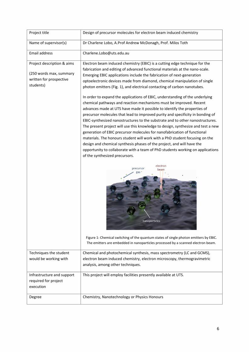
Electron beam induced chemistry (EBIC) is a cutting edge technique for the
fabrication and editing of advanced functional materials at the nano-scale.
Emerging EBIC applications include the fabrication of next-generation
optoelectronic devices made from diamond, chemical manipulation of single
photon emitters (Fig. 1), and electrical contacting of carbon nanotubes.
In order to expand the applications of EBIC, understanding of the underlying
chemical pathways and reaction mechanisms must be improved. Recent
advances made at UTS have made it possible to identify the properties of
precursor molecules that lead to improved purity and specificity in bonding of
EBIC-synthesized nanostructures to the substrate and to other nanostructures.
The present project will use this knowledge to design, synthesize and test a new
generation of EBIC precursor molecules for nanofabrication of functional
materials. The honours student will work with a PhD student focusing on the
design and chemical synthesis phases of the project, and will have the
opportunity to collaborate with a team of PhD students working on applications
of the synthesized precursors.
Figure 1: Chemical switching of the quantum states of single photon emitters by EBIC.
The emitters are embedded in nanoparticles processed by a scanned electron beam.
Techniques the student
would be working with
Chemical and photochemical synthesis, mass spectrometry (LC and GCMS),
electron beam induced chemistry, electron microscopy, thermogravimetric
analysis, among other techniques.
Infrastructure and support
required for project
execution
This project will employ facilities presently available at UTS.
Degree Chemistry, Nanotechnology or Physics Honours

7
Development of novel bio-markers based on fluorescent nanocrystals
A/Prof Igor Aharonovich ([email protected]), Dr Olga Shimoni
The goal of the project is to demonstrate use of nanodiamonds as bio-markers for biological tagging
and labelling. Nanodiamonds are biocompatible and host bright color centers which can be used as
efficient bio labels.
The project goals are to incorporation of the nanodiamonds into biological media – e.g. cells. Several
challenges will be addressed by the students during the project: prevention of nanodiamonds’
agglomeration, investigation of emitter photostability in small particles, characterization of
nanodiamonds in cells.
This multidisciplinary project will provide the student exposure to both optical and biological
sciences. The student will have access to the newly established nanophotonics laboratory that
includes a confocal microscope for the photoluminescence measurements as well as the opportunity
to learn basic biological processes and work with cells.
Techniques: Confocal microscopy, Scanning Electron Microscopy, biological sample preparation.
Investigation of optically active 2D materials
Dr Igor Aharonovich ([email protected]), Prof Milos Toth
Two dimensional materials (2D) such as graphene attract a lot of attention due to their unique
photophysical properties. Recently, it was shown that single layers of di-chalcogenides (MoS2/WS2)
are optically active materials that exhibit bright florescence.
This project will be focused on understanding the optical properties of these materials. The student
will investigate defect generation in these materials, perform high resolution spectroscopy and
measure photon statistics.
The student will have access to the materials and will investigate novel growth methods of single
layered materials. The newly established nanophotonics laboratory that includes all the required
optical gear (single photon detectors, spectrometer, low temperature cryostat etc) will be used for
characterization. The student will also get experience in nanomaterials characterization using SEM,
AFM and will pursue basic nanofabrication processes.
Techniques: Confocal microscopy, Scanning Electron Microscopy, chemical vapor deposition,
Cathodoluminescence, low temperature spectroscopy.

8
Coupling single emitters to plasmonic nanostructures
Dr Igor Aharonovich ([email protected]), Prof Mike Ford, Dr M. Arnold
The goal of the project is to develop robust methods to couple single emitters to plasmonic
nanostructures. One of the main challenges in single photon emitters is their relatively low
brightness. Through coupling to plasmonic resonators, the emission is enhanced and the excited
state lifetime is reduced.
The project will involve characterization of single photon emitters using a confocal microscope and
Hunbury Brown and Twiss interferometer. Once the emitters are selected, metal nanoparticles such
as gold and silver will be deterministically positioned in a close proximity to the emitters. To
optimize the coupling, various parameters including emitter’s distance, dipole orientation and the
plasmonic medium would be varied. If time permits, modeling of the system will be conducted to
understand the underlying photophysical processes.
The student will have access to the newly established nanophotonics laboratory that includes all the
required optical gear (single photon detectors, spectrometer, low temperature cryostat etc). The
student will also get experience in nanomaterials characterization using SEM, AFM and will pursue
basic nanofabrication processes.
Techniques: Confocal microscopy, Scanning Electron Microscopy, cathodoluminescence, low
temperature spectroscopy.
Controlled growth of diamond nanostructures
Dr Igor Aharonovich ([email protected]), Prof Milos Toth, Dr Olga Shimoni
The goal of the project is to develop growth of diamond nanoparticles and films using the newly
established microwave assisted chemical vapour deposition (CVD) reactor at UTS. One of the main
challenges will be controlling the density of the crystals, their final size and quality. A methodology
to incorporate fluorescent color centers into the diamond will be investigated as well.
The student will utilize the CVD reactor at UTS as well as the reactive ion etching system and
photolithography tools. This project will provide a thorough understanding into controlled growth of
diamond and fundamental nanofabrication techniques that will enable exposure to “real world”
technologically important processes. The student will also get experience in nanomaterials
characterization using SEM, and optical confocal microscopy.
Techniques: microwave CVD, photolithography, confocal microscopy, Scanning Electron Microscopy,
cathodoluminescence.

9
Project title Synthesis and optical properties of ‘cesium bronze’ and ‘sodium
bronze’
Name of supervisors Prof. Michael B Cortie, A/Prof. Andrew McDonagh
Email address [email protected]
Project description & aims
(250 words max, summary
written for prospective
students)
‘Tungsten bronzes’ are an unusual family of conducting oxides. They
can be manipulated to be metal-like, semi-conducting or insulating,
with an associated effect on their optical properties. They are of
interest for switchable windows and other active optical devices. In
this project we will investigate the chemical synthesis and the optical
properties of cesium and sodium tungsten bronzes. These have been
identified as having potential for application plasmonic and spectrally
selective applications. Our objective is to develop a material with
controllable band-gap and optimized dielectric function.
Techniques the student
would be working with
Wet chemical synthesis, X-ray diffraction, heat treatment in controlled
atmospheres, measurement of optical properties, Raman
spectroscopy
Infrastructure and support
required for project
execution
All facilities are available from within UTS.
Degree
Applied Physics, Nanotechnology, Applied Chemistry
10
Project title Structure of the mollusc shell
Name of supervisor(s) Dr Annette Dowd, Prof. Michael Cortie
Email address [email protected]
Project description & aims
(250 words max, summary
written for prospective
students)
Mollusc shells possess remarkable mechanical strength. Much of this
is due to a structural layer consisting of a composite of aragonite
(CaCO3) and protein. The protein acts like a glue and holds the crystals
of aragonite together, like mortar holds bricks together. Due to
diffraction of light, this is the layer that gives many mollusc shells their
nacreous lustre. Normally, there is also an outer layer of white CaCO3
with the calcite crystal structure. This layer is relatively brittle
compared to the nacreous layer. Recently, application of hi-resolution
Raman mapping at UTS has revealed that, in some species, there is an
intermediate layer that has a Raman spectrum matching aragonite yet
has a non-composite, non-nacreous microstructure. The purpose of
the present project is to find out what microstructure and properties
this intermediate layer actually has, whether such a layer is common
across a range of taxa (ie. different kinds of molluscs), and, if possible,
what its function might be for the organism.
Techniques the student
would be working with
Raman spectroscopy, analysis of Raman spectral data, optical and
scanning electron microscopy, X-ray diffraction, other characterization
techniques as needed or available
Infrastructure and support
required for project
execution
The necessary equipment is available at UTS.
Degree Applied Physics or Nanotechnology
11
Project title Quasi-ordered optical metamaterials
Name of supervisors Dr Matthew Arnold, Prof Michael Cortie
Email address [email protected]
Project description & aims
(250 words max, summary
written for prospective
students)
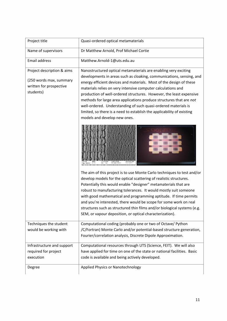
Nanostructured optical metamaterials are enabling very exciting
developments in areas such as cloaking, communications, sensing, and
energy efficient devices and materials. Most of the design of these
materials relies on very intensive computer calculations and
production of well-ordered structures. However, the least expensive
methods for large area applications produce structures that are not
well-ordered. Understanding of such quasi-ordered materials is
limited, so there is a need to establish the applicability of existing
models and develop new ones.
The aim of this project is to use Monte Carlo techniques to test and/or
develop models for the optical scattering of realistic structures.
Potentially this would enable “designer” metamaterials that are
robust to manufacturing tolerances. It would mostly suit someone
with good mathematical and programming aptitude. If time permits
and you’re interested, there would be scope for some work on real
structures such as structured thin films and/or biological systems (e.g.
SEM, or vapour deposition, or optical characterization).
Techniques the student
would be working with
Computational coding (probably one or two of Octave/ Python
/C/Fortran) Monte Carlo and/or potential-based structure generation,
Fourier/correlation analysis, Discrete Dipole Approximation.
Infrastructure and support
required for project
execution
Computational resources through UTS (Science, FEIT). We will also
have applied for time on one of the state or national facilities. Basic
code is available and being actively developed.
Degree Applied Physics or Nanotechnology
12
Project title Acceptors in zinc oxide nanowires
Name of supervisor(s) Dr Cuong Ton-That, Prof Matthew Phillips
Email address [email protected]
Project description & aims
(250 words max, summary
written for prospective
students)
Zinc oxide (ZnO) nanowires have the capability to provide the key for
many nanodevice applications due to its versatile optical and
electronic properties. ZnO also possesses properties superior to its
chief competitor, Gallium Nitride (GaN) that has been widely used in
light emitting diodes in recent years. Like nitride materials, benefits of
ZnO can only be realised once a reliable acceptor and associated
fabrication methods have been established.
Our recent studies have shown that ZnO nanowires doped with
nitrogen by plasma annealing exhibit the characteristics of a shallow
acceptor. However, the exact chemical origin of the acceptor has not
been established. This project involves the growth of ZnO nanowires
with prescribed defect properties using chemical vapour deposition.
Doping can be achieved in situ during the nanowire growth or as a
post-growth step. You will obtain experience in the synthesis and
characterisation of nanomaterials.
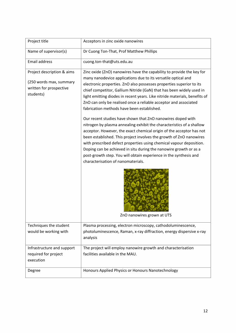
ZnO nanowires grown at UTS
Techniques the student
would be working with
Plasma processing, electron microscopy, cathodoluminescence,
photoluminescence, Raman, x-ray diffraction, energy dispersive x-ray
analysis
Infrastructure and support
required for project
execution
The project will employ nanowire growth and characterisation
facilities available in the MAU.
Degree Honours Applied Physics or Honours Nanotechnology

13
Project title Thin film architectures for spectral and angular control of light
Name of supervisors Dr Matthew Arnold and Dr Angus Gentle
Email address [email protected]
Project description & aims
(250 words max, summary
written for prospective
students)
Controlling “radiance”, the amount of optical energy passing into and
out of a surface, is key for leveraging advances in optical science for
application to energy efficient buildings. In particular, novel thin film
designs should allow control of spectral and angular radiance in new
ways (e.g. coatings that keep buildings cooler than the surroundings
http://newsroom.uts.edu.au/news/2015/05/super-cool-roof-solution-
being-hot-city, coatings that only allow one angle to pass http://ab-
initio.mit.edu/~ycshen/angularselective/).
A cool roof material, photo by Angus via the UTS news room.
The aim of this project is to design, produce and test thin film stacks
that have desirable spectral and angular properties. Some of the
inspiration and/or materials may come from biological systems. There
is considerable scope for choosing your direction in this project, but it
would ideally suit someone with good technical and analytical
aptitude.
Techniques the student
would be working with
Thin film design software, vacuum deposition, advanced
spectrophotometry, ellipsometry, XRD, EDS
Infrastructure and support
required for project
execution
See techniques – all infrastructure is already available and in-place.
Makes use of newly purchased state-of-the-art optical
characterization equipment (VASE ellipsometer & Agilent UMS).
Degree
Honours Applied Physics or Honours Nanotechnology
14
Project title 2 Dimensional Materials
Name of supervisor(s) A/Prof Mike Ford
Email address [email protected]
Project description & aims
(250 words max, summary
written for prospective
students)
Graphene is the most famous and most widely studied single atom
thick or 2D material. There are now a number of alternative 2D
materials that have been discovered, for example MoS2, silicene,
phosphorene etc that all have equally promising properties and
applications in, for example, electronic devices. Combinations of
different 2D layers to build so-called van der Waals hetrostructures is
even more promising because it provides access to a huge range of
material properties and the ability to tune these properties.
Combining these materials experimentally is very challenging and has
limited advances in this field. This is where computer simulations, or
experiments conducted in-silico, are invaluable as they overcome
these problems. The aim of this project is to use calculations to
identify new van der Waals hetrostructures that could be used, for
example, as single photon sources in quantum communication.
The research will give you an introduction to the rapidly growing field
of 2D materials, experience at solving problems using numerical
techniques and using high performance computing systems.
There is potential for more than one honours project working in this
area supervised by me.
Techniques the student
would be working with
Computer based materials programs for calculating the properties of
materials (eg VASP or SIESTA). Depending upon interest there is also
opportunity to write your own programs.
Infrastructure and support
required for project
execution
High performance computing facilities. We have access to the 57,472
processor supercomputer in Canberra, and the 3,328 processor Cray
supercomputer in Perth.
Degree Honours Nanotechnology or Honours Applied Physics