LINEAR OPTICAL EFFECTS IN NANOSTRUCTURED SOLIDS
36
Oulu University August 28, 2008 M.V. Lomonosov Moscow State University, Physics Department Russian Research Center “Kurchatov Institute” LINEAR OPTICAL EFFECTS IN LINEAR OPTICAL EFFECTS IN NANOSTRUCTURED SOLIDS NANOSTRUCTURED SOLIDS Pavel Kashkarov Lecture 1
-
Upload
abigail-ewing -
Category
Documents
-
view
34 -
download
4
description
Lecture 1. LINEAR OPTICAL EFFECTS IN NANOSTRUCTURED SOLIDS. Pavel Kashkarov. M.V. Lomonosov Moscow State University, Physics Department Russian Research Center “Kurchatov Institute”. Outline. Introduction Photonic crystals and anisotropic layers based on porous silicon - PowerPoint PPT Presentation
Transcript of LINEAR OPTICAL EFFECTS IN NANOSTRUCTURED SOLIDS

Oulu University August 28, 2008
M.V. Lomonosov Moscow State University, Physics Department
Russian Research Center “Kurchatov Institute”
LINEAR OPTICAL EFFECTS IN LINEAR OPTICAL EFFECTS IN
NANOSTRUCTURED SOLIDSNANOSTRUCTURED SOLIDS
Pavel Kashkarov
Lecture 1

Oulu University August 28, 2008
I. Introduction
II. Photonic crystals and anisotropic
layers based on porous silicon
III. Silicon nanocrystals in dielectric matrix
for optoelectronic applications
IV. Silicon nanocrystals for biomedical
applications
V. Conclusions
Outline

Oulu University August 28, 2008
1. The idea that nanostructuring of homogenous and isotropic media results in completely new optical properties was suggested many years ago (see excellent textbook “Principles of Optics” by M. Born and E. Wolf). But at that time there was not appropriate technology to fabricate nanostructured materials.
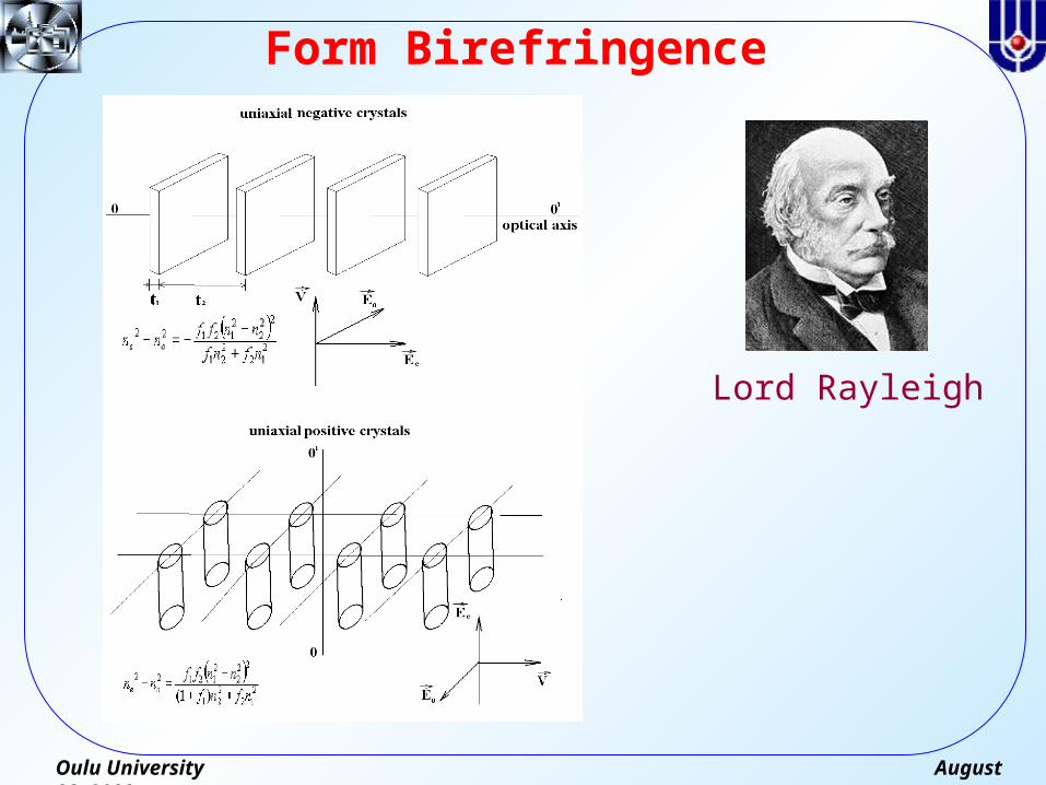
2. There were suggested two types of structures with form anisotropy: parallel layers and periodically arranged nanocylinders. Both structures show a strong birefringence.
Photonic crystals and anisotropic layers based on porous silicon
Oulu University August 28, 2008
Form Birefringence
Lord Rayleigh

Oulu University August 28, 2008
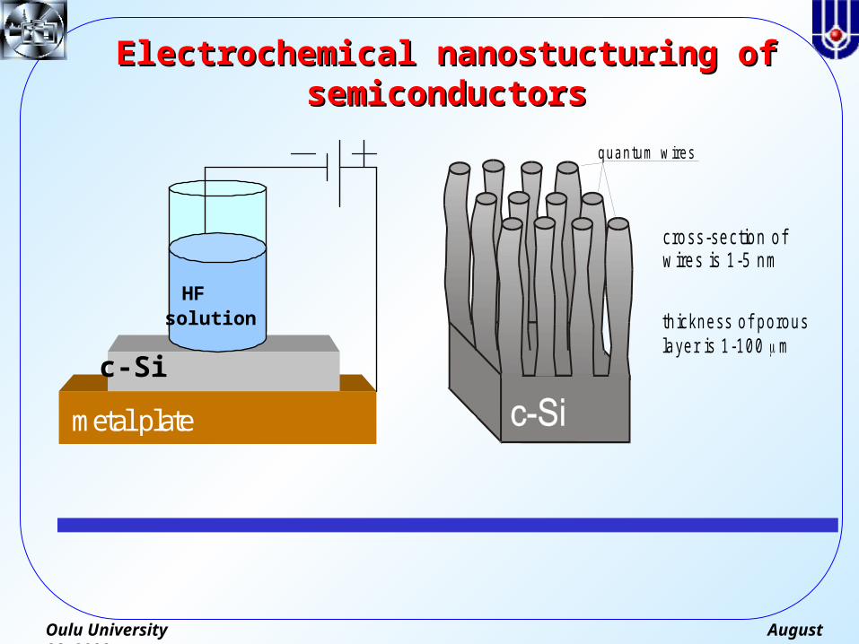
3. Only recently an electrochemical technique was applied to fabricate such structures on semiconductor substrate (mainly silicon).
4. Another type of an artificial medium is a photonic crystal. It turns out that it also can be easily made by the electrochemical treatment of semiconductors.
5. The obvious advantage of porous nanostructured media is the possibility to change the optical properties of the sample by filling pores by different gaseous, liquid and solid substances.
...... Photonic crystals and anisotropic layers based on porous silicon
Oulu University August 28, 2008
Electrochemical nanostucturing of Electrochemical nanostucturing of semiconductorssemiconductors
cross-section ofw ires is 1-5 nm
th ickness of porouslayer is 1-100 m
quantum w ires
metal plate
HFsolution
c-Si

Oulu University August 28, 2008
Different morphologies of porous siliconDifferent morphologies of porous silicon
Preferential pore growth in <100> crystallographyc directionmicroporous
(100) surface, =10 cm
mesoporous
(110) surface, =3 mcm

Oulu University August 28, 2008
Tailoring of the Refractive Index by Tailoring of the Refractive Index by NanostucturingNanostucturing
Effective media approximation(Bruggeman model )
eff of the disordered heterogeneous mixture:
0)1(22
eff
Si
eff
Sieff
d
eff
d PP
where P is porosity
refractive index: eff
n
0 50 100 150 200 250 300
40
50
60
70
80
p-Si (75 mcm)
Po
rosi
ty (
%)
Current Density (mA/cm2)
2.6
2.4
2.2
2.0
1.8
1.6
1.4
Re
fra
ctiv
e in
de
x

Oulu University August 28, 2008
10000 15000 20000 25000 30000 350000.0
0.2
0.4
0.6
0.8
1.0
Ref
lect
ivity
Wavenumber (cm-1)
1200 900 600 300
photonic
bandgap
Wavelength (nm)
Ideal Bragg reflector
12 pairs n1=1.3, n2=2
Porous Silicon Based Photonic CrystalsPorous Silicon Based Photonic Crystals
c-Si
n1d1+n2d2=/2
0 10 20 30 40 50 60 70 80 90 100
0
20
40
60
80
100
Cu
rre
nt d
en
sity
(m
A/c
m2 )
time (sec)
Bragg condition:

Oulu University August 28, 2008
n1
n2
1D 1D PPhotonic hotonic CCrystal rystal BBased oased onn PPorous orous SSiliconilicon
d2
d1

Oulu University August 28, 2008
Linear Linear OOptical ptical PProperties of roperties of PPhotonic hotonic CCrystalrystalss BBased oased onn PPorous orous SSiliconilicon
0,0
0,5
1,00,0
0,5
1,0
8 11 14 17 20 23 260,0
0,5
1,0
(B)
Ref
lect
ivity
(A)
(C)
Wavenumber ( 103 cm-1)
1,2 1 0,8 0,6 0,4
Wavelength (m)

Oulu University August 28, 2008
Strong Strong OOptical ptical AAnisotropy in (110) nisotropy in (110) PPorous orous SSiliconilicon
n 0 0 1 < n 1 - 1 0
( 1 1 0 )
[ 0 1 0 ] [ 1 0 0 ]
n 0 0 1 > n 1 - 1 0
[ 1 - 1 0 ]
[ 0 0 1 ]
e
S i
d
0)()(
)1(,2
,2
,1
,1
iieffieff
iieff
iieffieff
iieff
Lp
Lp
Generalized
Bruggeman model

Oulu University August 28, 2008
Effect of Effect of PorosityPorosity on on BBirefringence of irefringence of NNanostructured anostructured SSilicon ilicon FFilmsilms
Nanostructured Si films have large birefringence value δn =18%
medium Δn
Crystalline Si 5 10-6
Iceland spar 0.15Por-Si (110) 0.24
For layers prepared at j =100 mA/cm2 :
Δn=0.24<n> = (no+ne)/2 = 1.3
δn=Δn/<n> = 0.181.2
1.4
1.6
1.8
2.0
25 50 75 100
0.0
0.1
0.2
0.3
0.4
ne
no
Ref
ract
ive
inde
x
porosity
80%
60%
65%
Current density, mA/cm2
n o-n e
Oulu University August 28, 2008
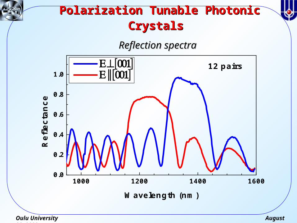
Polarization Polarization TTunable unable PPhotonic hotonic CCrystalsrystals
1000 1200 1400 16000.0
0.2
0.4
0.6
0.8
1.0
12 pairs
R
efle
ctan
ce
Wavelength (nm)
Reflection spectraReflection spectra

Oulu University August 28, 2008
Oxidized Porous SiliconOxidized Porous Silicon
• Thermal oxidation of birefringent por-Si film results in formation of chemically stable, transparent for visible radiation medium, which possesses optical anisotropy.
Por-Si
X-ray diffraction
c-Si Oxydized por-Si

Oulu University August 28, 2008
950 oC 2.5 h
Transparent birefringent film
Oxidized por-Si film on a mirror under a polarizer.
10 20 30 40 50 60 70 80 900.005
0.010
0.015
0.020
0.025
|no -
n e|
Current density (mА/сm2)
In oxidized por-Si birefringence is 2 times higher than in quartz
Birefringence of Oxidized Porous SiliconBirefringence of Oxidized Porous Silicon

Oulu University August 28, 2008
1. Silicon was, is and will be the main material for microelectronics, but application of silicon in optoelectronics is limited.
2. Low probability of radiative electron transition in Si can be increased by formation of nanoparticles or/and by an introduction of activators of luminescence.
3. A Er3+ ion possesses rather promising properties as a luminescence activator in Si. The Er3+ luminescence line (λ=1.54µm) corresponds to a maximum of transmission in the quartz fiber waveguides.
4. For formation of light emitting device we combined both approaches
Silicon nanocrystals in dielectric matrix for optoelectronic applications

Oulu University August 28, 2008
Light absorption in semiconductors (interband transitions)
1. Direct gap materials (GaAs, InP, CdTe, CdS )
*h
v*e
gc m
pp
m
pEp
2)(,
2)(
22
f
i0 –
0
Eg
Е
h Eg
p
<111> <000> <100>
LGaAs
Eg=1.52 эВ
Е
p
hvc
vc
h
vch
vc
pp
cmaahp
cmhp
ppp
EEh
,
700,
34
)10(/
)1010(/
0

Oulu University August 28, 2008
Light absorption in semiconductors (interband transitions)
2. Indirect gap materials (Ge, Si, GaP )
phonvch
vc
pppp
EEh
3. Heisenberg uncertainty principle
,2/
2/
dp
xp
where d is a nanoparticle size

Oulu University August 28, 2008
Quantum size effect
EEE
mmd
nhEEE
md
nh
m
pEdhnp
ndnph
gg
hehe
ee
eee
eee
0
**2
22
*2
22
*
2
11
4
42;2/
,...2,1,2/;/

Oulu University August 28, 2008
Quantum size effect
vcEEh
2D structure
Quantum size effect enables one to modify absorption and luminescence spectra of semiconductor nanoparticles
The effect becomes appreciable when the size of a particle is less then 10 nm

Oulu University August 28, 2008
Size-controlled Si nanocrystals in nc-Si/SiOSize-controlled Si nanocrystals in nc-Si/SiO22
SuperlatticesSuperlattices
Preparation Details:
1. Alternating evaporation of SiO powder in vacuum 10-7 mbar or in oxygen atmosphere under oxygen partial pressure of 10-4 mbar. This changes the stoichiometry x of SiOx alternatively between 1 and 2.
2. SiO/SiO2 superlatticies are characterized by the thickness of the SiO layers varied between 1 and 3 nm and the thickness of SiO2 layers between 2 and 3 nm. The number of periods varied between 30 and 90.
3. The evaporated samples were annealed at 1100 oC under N2 atmosphere. Thus nc-Si/ SiO2 superlattices were obtained. were obtained.
4. Er doped nc-Si/SiO2 superlattice were produced by implantation with Er ions (energy 300 keV, doses 1014 – 5·1016 cm-2) followed by TA at 900 oC for 5-60 minutes.
3nm
M. Zacharias et al., APL 80, 661 (2002).
Er

Oulu University August 28, 2008
Size Dependent PL of nc-Si/SiOSize Dependent PL of nc-Si/SiO22
Structures Structures
Size of Si nanocrystals is controlled by initial thickness of SiO layer in SiO/SiO2 superlattice
The peak position of PL spectrum is determined by quantum confinement and excitonic effects in Si nanocrystals in SiO2 matrix.
1.0 1.2 1.4 1.6 1.8 2.0
No
rma
lize
d P
L I
nte
ns
ity
Photon Energy (eV)
dSiO
= 6 ... 2 nm

Oulu University August 28, 2008
Effect of Er doping on PL of nc-Si/SiOEffect of Er doping on PL of nc-Si/SiO22
Er doping results in both two order of magnitude quenching of the exciton PL and a strong emission line at 1.5 m
Er-doped a-SiO2 layers does not exhibit efficient Er photoluminescence
Efficient energy transfer from electronic excitation of Si nanocrystals to Er ions
0.8 1.0 1.2 1.4 1.6 1.8 2.0
10-3
10-2
10-1
100
4F9/2
-4I15/2
4I9/2
-4I15/2
4I11/2
-4I15/2
4I13/2
-4I15/2
hexc
= 3.7 eVT= 300 K
nc-Si/SiO2
dSi = 3 nm
nc-Si/SiO2
nc-Si/SiO2:Er
a-SiO2:Er
PL
Inte
nsity
(ar
b. u
n.)
Photon Energy (eV)
Er3+
1.5 m(0.8 eV)
P.K.Kashkarov et al., JETP 64,1123 (2003)

Oulu University August 28, 2008
Transient PL Investigation of ErTransient PL Investigation of Er3+3+ Population Population InversionInversion
• Lifetime of Er-related PL becomes shorter at Iexc > 0.1 W/cm2 that correlates with the population inversion of Er3+
0.01 0.1 1
1
2
3
4
5
nc-Si/SiO2:Er
d=4 nm
decay
rise
Tim
e (
ms)
Pump power (W/cm2)0.01 0.1 1
0.1
1
N1/N
Er= 1 -
rise/
decay
N1/N
Er
Pump power (W/cm2)
0.5
N1
N0

Oulu University August 28, 2008
Silicon nanocrystals for biomedical Silicon nanocrystals for biomedical applicationsapplications
1. Oxygen molecules exist in several forms: non-active one (ground state) and active ones (excited states)
2. In the active form oxygen is toxic and therefore fatal for any live cells
3. This property of active oxygen is used to clean water containing harmful microbes and is the base of our immunity
4. In some cases generation of active oxygen can be applied for cancer therapy
5. But how an oxygen molecule can be transferred into active form?
Oulu University August 28, 2008
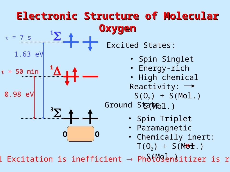
1
O O
1.63 eV
0.98 eV
3
1
Optical Excitation is inefficient Photosensitizer is required
Excited States:
• Spin Singlet• Energy-rich• High chemical Reactivity: S(O2) + S(Mol.) S(Mol.)
Ground State:
• Spin Triplet• Paramagnetic• Chemically inert: T(O2) + S(Mol.) S(Mol.)
= 7 s
= 50 min
Electronic Structure of Molecular OxygenElectronic Structure of Molecular Oxygen

Oulu University August 28, 2008
Photosensitization: Basic PrinciplePhotosensitization: Basic Principle
Efficient Energy Transfer requires: Small Spatial Separation between Donor and Acceptor
• Spectral Overlap of Donor and Acceptor Energy Bands• High Quantum Efficiency of Donor Luminescence
Donor Acceptor
S0
S1
S
T
T0
Energy Transfer
h
R

Oulu University August 28, 2008
Si Nanocrystal Assemblies as Photosensitizers?Si Nanocrystal Assemblies as Photosensitizers?
1.2 1.4 1.6 1.8 2.0 2.2 2.4
0.0
0.5
1.0 FE(Si)
PL
In
ten
sit
y (
arb
.un
its
)
Energy (eV)
A.G.Cullis and L.T.Canham, Nature 353, 335 (1991)
1.2 1.4 1.6 1.8 2.0 2.2 2.4
101
102
103
S
T
S
Energy (eV)
Ex
cit
on
Lif
eti
me
(µ
s)
•Simple Electrochemical Preparation •Open Nanostructure•Efficient Photolumenescence
• Broad Tunable Emission Band • Long Exciton Lifetime (µs - ms)

Oulu University August 28, 2008
0.8 1.2 1.6 2.0
10 -4
10 -3
10 -2
10 -1
100 T=5 K Vacuum Physisorbed O
2
1 3
1
Energy (eV)
PL
In
ten
sit
y (
arb
. u
nit
s)
Effect of Physisorbed Oxygen Molecules on Effect of Physisorbed Oxygen Molecules on PL of Si Nanocrystal AssemblyPL of Si Nanocrystal Assembly
Evidence for Energy Transfer from Excitons to O2
• PL Quenching of Excitonic and Defect Emission Band
• 1 3 Emission Line of 1O2

Oulu University August 28, 2008
Singlet Oxygen Photosensitization in WaterSinglet Oxygen Photosensitization in Water
1 mg of nano-Si (from micropor-Si) dispersed in 3 ml of
H2O
%40E
for SO ~ 1-3 s: NSO ~ 1015 – 1016 (1/cm3)
7.1)()( oxygen
PLvac
PL dttIdttI

Oulu University August 28, 2008
Effect of Porous Si on cancer cellsEffect of Porous Si on cancer cells(in vitro experiments with mouse fibroblasts)(in vitro experiments with mouse fibroblasts)
Cancer cell number vs porous Si concentration in the dark (blue symbols) and after illumination (red symbols)
Cells were counted by using optical density measurements

Oulu University August 28, 2008
DNA AnalysisDNA Analysis
Histogram of DNA content for the cancer cells kept in the nutrient solution with dispersed Histogram of DNA content for the cancer cells kept in the nutrient solution with dispersed porous Si (1.5 g/l) in darkness (blue curve) and after illumination (red curve). Symbols G1, S, porous Si (1.5 g/l) in darkness (blue curve) and after illumination (red curve). Symbols G1, S, and G2 mark different cycles of the cell proliferation. The apoptotic cell region is marked by and G2 mark different cycles of the cell proliferation. The apoptotic cell region is marked by A. Inset shows the relative contribution of G1, S and G2 regions A. Inset shows the relative contribution of G1, S and G2 regions vsvs nc-Si concentration in the nc-Si concentration in the dark (blue symbols) and after illumination (red symbols)dark (blue symbols) and after illumination (red symbols)
Oulu University August 28, 2008
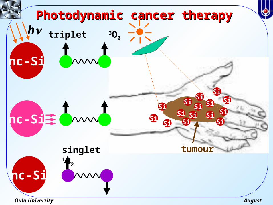
Photodynamic cancer therapyPhotodynamic cancer therapy
nc-Si
tumour
Si Si
SiSi
Si
SiSi
Si
Si
Si
Si
SiSi
SiSi
nc-Si
nc-Si
h triplet 3О2
singlet 1О2
Oulu University August 28, 2008
General Conclusions • Nanostructuring of homogenous and isotropic
Si-crystals enables one to form photonic media with unique properties
• Ensembles of Si-nanocrystals in a dielectric matrix are promising base for silicon laser compatible with microelectronic technology
• Bio-compatible Si-nanoparticles are effective photosensitizers of singlet oxygen generation what can be applied for photodynamic cancer therapy

Oulu University August 28, 2008
Thank you for the attention!