
Lightning (DSPC-8681E) User Guide -...
39
Lightning (DSPC-8681E) User Guide Revision v0.6 Initiated by Holland Huang Sungyi Chen Job Title Supervisor Senior Engineer Signature Approved by Dick Lin Job Title Software Manager Signature 2 nd Approved Job Title Signature Release Status Release Date
Transcript of Lightning (DSPC-8681E) User Guide -...
Lightning
(DSPC-8681E)
User Guide Revision v0.6
Initiated by Holland Huang
Sungyi Chen
Job
Title
Supervisor
Senior Engineer
Signature
Approved
by
Dick Lin Job
Title
Software Manager Signature
2nd
Approved
Job
Title
Signature
Release
Status
Release
Date

Revision History
Version Date Author Description
0.1 08/08/11 Sungyi Chen
Holland Huang
Initial draft.
0.2 09/26/11 Holland Huang The version number of this document is change to
synchronize with SW package 0.2.
0.3 10/20/11 Jason Hsueh 1. The SW package 0.3 support MCSDK
version 2.0.3.15.
2. Add image processing example.
0.4 01/11/12 Holland Huang 1. Add memory read/write function in DSP
loader.
2. Driver modification to ensure stability of
memory read/write
3. Support both Legacy and MSI interrupt in ipc
example.
0.5 06/19/12 Holland Huang 1. The SW package 0.5 support MCSDK version
2.00.09.21
2. Support memory writing into chip cfg space in
PCIe driver.
3. Add DMA read/write function in PCIe driver.
0.6 11/16/12 Holland Huang 1. The SW package 0.6 support Samsung 4G
DDR module.
2. Add subsystem ID and subsystem vendor ID
3. Add I2C boot from address 0x50 to support
64bits address BAR.
Content
1. Introduction ................................................................................................................................... 5
1.1. Hardware Description ....................................................................................................... 5
1.2. DSPC-8681E Block Diagram ............................................................................................... 6
1.3. DDR3 Interface .................................................................................................................. 6
1.4. PCIe Interface .................................................................................................................... 7
1.5. HyperLink Interface ........................................................................................................... 7
1.6. Serial RapidIO Interface..................................................................................................... 7
1.7. SGMII Interface ................................................................................................................. 7
1.8. DSP Identification .............................................................................................................. 8
1.9. Hardware Environment Setting ......................................................................................... 9
2. Package Content........................................................................................................................... 12
2.1. API Interface of DSP Driver.............................................................................................. 12
2.2. DSP Program Loader Utility ............................................................................................. 13
2.3. Example: DDR3 Initialization ........................................................................................... 13
2.4. Example: Simple Web Server .......................................................................................... 14
2.5. Example: PC/DSP Communication .................................................................................. 14
2.6. Example: Image Processing ............................................................................................. 14
2.7. Patch: Platform Library and NDK Library ........................................................................ 14
3. DSP Program Loader..................................................................................................................... 15
3.1. Host System Requirement .............................................................................................. 15
3.2. Build Instruction .............................................................................................................. 15
3.2.1. Build the Driver .................................................................................................. 15
3.2.2. Build the Utility .................................................................................................. 15
3.3. Installation and Usage ..................................................................................................... 16
3.4. DSP Loader Utility ............................................................................................................ 18
3.4.1. Query DSP Information ...................................................................................... 18
3.4.2. Download DSP Program Image .......................................................................... 19
3.4.3. DSP memory read .............................................................................................. 20
3.4.4. DSP memory write ............................................................................................. 21
4. Reference Implementations ......................................................................................................... 23
4.1. Patch of Platform Library and NDK Library ..................................................................... 23
4.1.1. Build Instruction ................................................................................................. 23
4.2. DSP DDR3 Initialization.................................................................................................... 25
4.2.1. Build Instruction ................................................................................................. 25
4.2.2. Usage .................................................................................................................. 25
4.3. Ethernet and Simple Web Server .................................................................................... 26
4.3.1. Build Instruction ................................................................................................. 26
4.3.2. Usage .................................................................................................................. 27
4.4. Communication between PC and DSP ............................................................................ 29
4.4.1. Build Instruction ................................................................................................. 29
4.4.2. Usage .................................................................................................................. 30
4.4.3. Console Simulation ............................................................................................. 31
4.4.4. DSP Demo Program ............................................................................................ 32
4.5. Image Processing Demonstration ................................................................................... 34
4.5.1. Build Instruction ................................................................................................. 35
4.5.2. Usage .................................................................................................................. 35
1. Introduction
This document describes how to set up the software configurations for quad-DSP PCIe
board, called Lightning (DSPC-8681E), before using it. The Lightning board contains four
Texas Instruments TMS320C6678 DSPs with PCIe, HyperLink, Serial RapidIO, and SGMII
interfaces.
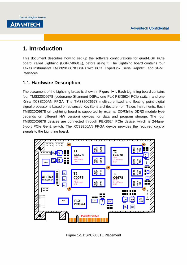
1.1. Hardware Description
The placement of the Lightning broad is shown in Figure 1−1. Each Lightning board contains
four TMS320C6678 (codename Shannon) DSPs, one PLX PEX8624 PCIe switch, and one
Xilinx XC3S200AN FPGA. The TMS320C6678 multi-core fixed and floating point digital
signal processor is based on advanced KeyStone architecture from Texas Instruments. Each
TMS320C6678 on Lightning board is supported by external DDR3(the DDR3 module type
depends on different HW version) devices for data and program storage. The four
TMS320C6678 devices are connected through PEX8624 PCIe device, which is 24-lane,
6-port PCIe Gen2 switch. The XC3S200AN FPGA device provides the required control
signals to the Lightning board.
Figure 1-1 DSPC-8681E Placement
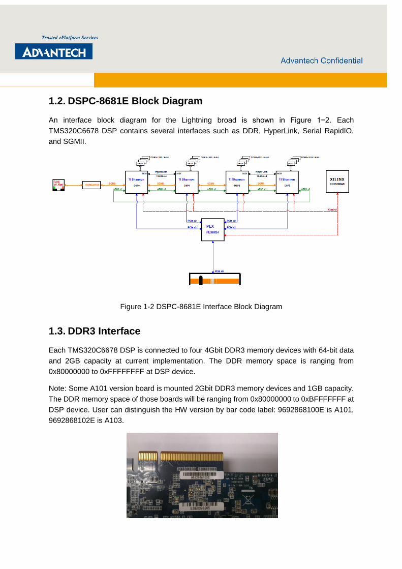
1.2. DSPC-8681E Block Diagram
An interface block diagram for the Lightning broad is shown in Figure 1−2. Each
TMS320C6678 DSP contains several interfaces such as DDR, HyperLink, Serial RapidIO,
and SGMII.
Figure 1-2 DSPC-8681E Interface Block Diagram
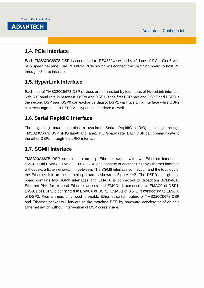
1.3. DDR3 Interface
Each TMS320C6678 DSP is connected to four 4Gbit DDR3 memory devices with 64-bit data
and 2GB capacity at current implementation. The DDR memory space is ranging from
0x80000000 to 0xFFFFFFFF at DSP device.
Note: Some A101 version board is mounted 2Gbit DDR3 memory devices and 1GB capacity.
The DDR memory space of those boards will be ranging from 0x80000000 to 0xBFFFFFFF at
DSP device. User can distinguish the HW version by bar code label: 9692868100E is A101,
9692868102E is A103.
1.4. PCIe Interface
Each TMS320C6678 DSP is connected to PEX8624 switch by x2-lane of PCIe Gen2 with
5Gb speed per lane. The PEX8624 PCIe switch will connect the Lightning board to host PC
through x8-lane interface.
1.5. HyperLink Interface
Each pair of TMS320C6678 DSP devices are connected by four lanes of HyperLink interface
with 50Gbaud rate in between. DSP0 and DSP1 is the first DSP pair and DSP2 and DSP3 is
the second DSP pair. DSP0 can exchange data to DSP1 via HyperLlink interface while DSP2
can exchange data to DSP3 via HyperLink interface as well.
1.6. Serial RapidIO Interface
The Lightning board contains a two-lane Serial RapidIO (sRIO) chaining through
TMS320C6678 DSP sRIO lane0 and lane1 at 5 Gbaud rate. Each DSP can communicate to
the other DSPs through the sRIO interface.
1.7. SGMII Interface
TMS320C6678 DSP contains an on-chip Ethernet switch with two Ethernet interfaces,
EMAC0 and EMAC1. TMS320C6678 DSP can connect to another DSP by Ethernet interface
without extra Ethernet switch in between. The SGMII interface connection and the topology of
the Ethernet link on the Lightning broad is shown in Figure 1−2. The DSP0 on Lightning
board contains two SGMII interfaces and EMAC0 is connected to Broadcom BCM54616
Ethernet PHY for external Ethernet access and EMAC1 is connected to EMAC0 of DSP1.
EMAC1 of DSP1 is connected to EMAC0 of DSP2. EMAC1 of DSP2 is connecting to EMAC0
of DSP3. Programmers only need to enable Ethernet switch feature of TMS320C6678 DSP
and Ethernet packet will forward to the matched DSP by hardware accelerator of on-chip
Ethernet switch without intervention of DSP cores inside.
1.8. DSP Identification
The Lightning board use GPIO[1:2] pins to identify each DSP and the assignment of DSP ID
is shown below:
GPIO 2 GPIO 1
DSP 0 0 0
DSP 1 0 1
DSP 2 1 0
DSP 3 1 1
Table 1-1 DSP ID and GPIO table
The Linux command “lspci” can list which type of board it is running by checking subsystem
ID and subsystem vendor ID as table 1-2.
SUBSYS_ID SUBSYS_VEN_ID
Value 0x8681 0x13FE
Table 1-2 Subsystem ID and vendor ID table
#lspci -vvnn -d:b005
04:00.0 Multimedia controller [0480]: Texas Instruments Device [104c:b005] (rev
01)
Subsystem: Advantech Co. Ltd Device [13fe:8681]
Control: I/O+ Mem+ BusMaster+ SpecCycle- MemWINV- VGASnoop- ParErr-
Stepping- SERR- FastB2B- DisINTx-
Status: Cap+ 66MHz- UDF- FastB2B- ParErr- DEVSEL=fast >TAbort- <TAbort-
<MAbort- >SERR- <PERR- INTx-
Latency: 0, Cache Line Size: 64 bytes
Interrupt: pin A routed to IRQ 11
Region 0: Memory at f8800000 (32-bit, non-prefetchable) [size=4K]
Region 1: Memory at df000000 (32-bit, prefetchable) [size=16M]
Region 2: Memory at de000000 (32-bit, prefetchable) [size=16M]
Region 3: Memory at dc000000 (32-bit, prefetchable) [size=32M]
Region 4: Memory at d8000000 (32-bit, prefetchable) [size=64M]
Capabilities: <access denied>
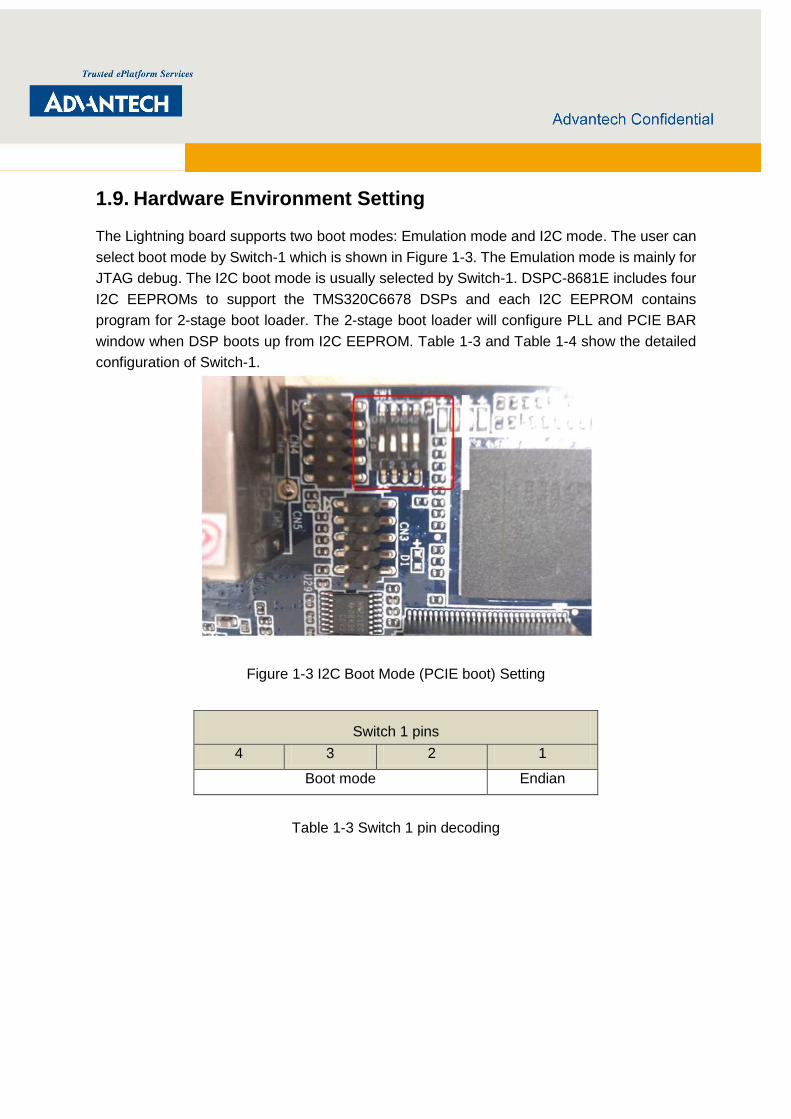
1.9. Hardware Environment Setting
The Lightning board supports two boot modes: Emulation mode and I2C mode. The user can
select boot mode by Switch-1 which is shown in Figure 1-3. The Emulation mode is mainly for
JTAG debug. The I2C boot mode is usually selected by Switch-1. DSPC-8681E includes four
I2C EEPROMs to support the TMS320C6678 DSPs and each I2C EEPROM contains
program for 2-stage boot loader. The 2-stage boot loader will configure PLL and PCIE BAR
window when DSP boots up from I2C EEPROM. Table 1-3 and Table 1-4 show the detailed
configuration of Switch-1.
Figure 1-3 I2C Boot Mode (PCIE boot) Setting
Switch 1 pins
4 3 2 1
Boot mode Endian
Table 1-3 Switch 1 pin decoding
Bit Field Value Description
4~2 Boot mode 111
110
100
Others
Emulation boot mode
I2C boot mode(Boot from address 0x51)
32bits address BAR setting
I2C boot mode(Boot from address 0x50)
64bits address BAR setting
Reserved
1 Endian 0
1
Little endian
Big endian
Table 1-4 Switch-1 Configuration Bit Field Description
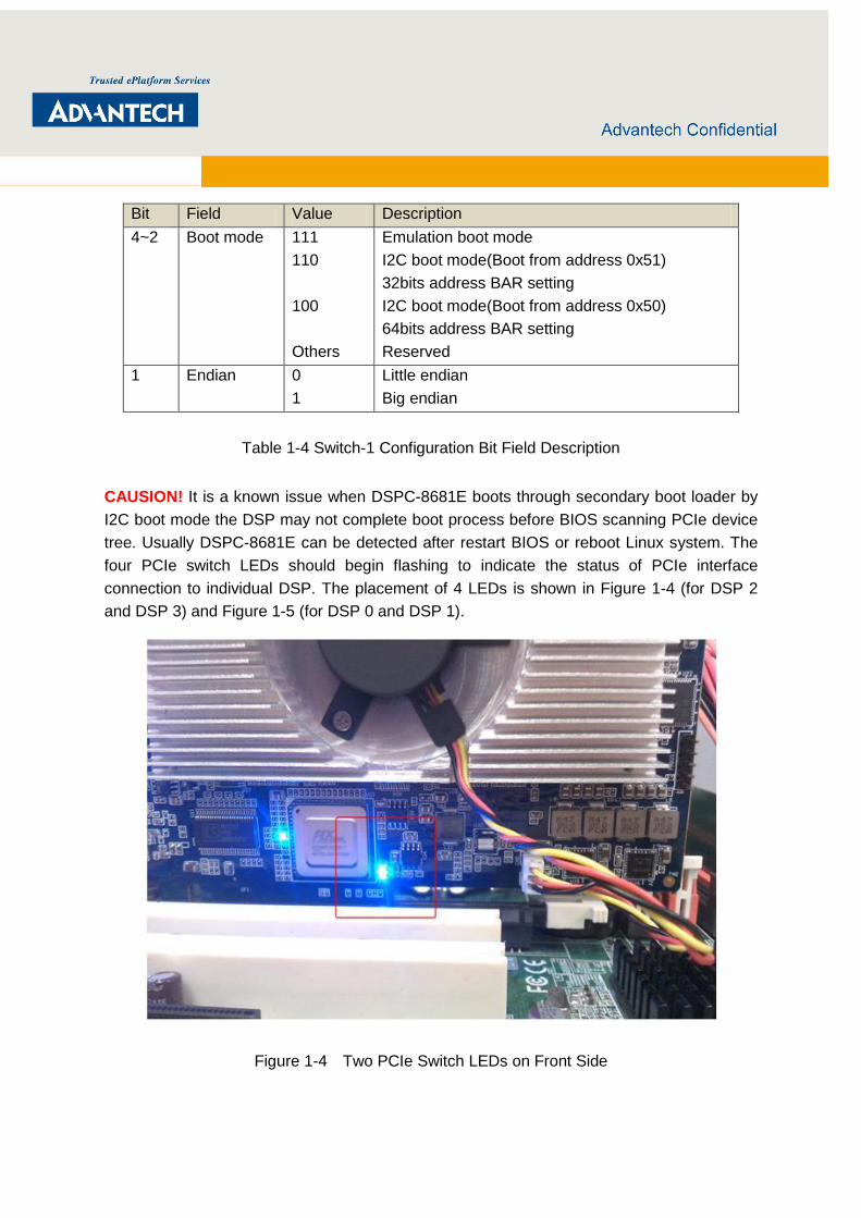
CAUSION! It is a known issue when DSPC-8681E boots through secondary boot loader by
I2C boot mode the DSP may not complete boot process before BIOS scanning PCIe device
tree. Usually DSPC-8681E can be detected after restart BIOS or reboot Linux system. The
four PCIe switch LEDs should begin flashing to indicate the status of PCIe interface
connection to individual DSP. The placement of 4 LEDs is shown in Figure 1-4 (for DSP 2
and DSP 3) and Figure 1-5 (for DSP 0 and DSP 1).
Figure 1-4 Two PCIe Switch LEDs on Front Side
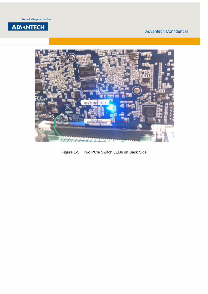
Figure 1-5 Two PCIe Switch LEDs on Back Side
2. Package Content
This package is created to help customer quickly boot DSP through PCIE, the package
includes:
Path Purpose
Lightning_PCIE/dsp_loader/driver DSP Program Loader Driver
Lightning_PCIE/dsp_loader/app DSP Program Loader Utility
Lightning_PCIE/examples/ddr3 Example: DDR3 Initialization
Lightning_PCIE/examples/web Example: Simple Web Server
Lightning_PCIE/examples/ipc Example: PC/DSP Communication
Lightning_PCIE/examples/image_processing Example: Image Processing using Multi-Core
Lightning_PCIE/patch Patch: Platform Library and NDK Library of
PDK C6678 1.0.0.21 (inside MCSDK 2.0.9.21)
Table 2-1 Package content list
2.1. API Interface of DSP Driver
It is a Linux based PCIE driver which is used to map between PC memory and DSP memory,
it supports the access of 32 DSPs (8 DSPC-8681E card) at most. Currently, the implemented
I/O control is listed below:
IOCTL code Description
TI667x_PCIEEP_IOCTL_DSP_MSI0_SET Generate a MSI interrupt 0 to DSP
TI667x_PCIEEP_IOCTL_DSP_MSI0_CLR Clear MSI0 interrupt
TI667x_PCIEEP_IOCTL_DSP_INTA_SET Generate a legacy interrupt A to DSP
TI667x_PCIEEP_IOCTL_DSP_INTA_CLR Clear legacy interrupt A
TI667x_PCIEEP_IOCTL_DSP_INTB_SET Generate a legacy interrupt B to DSP
TI667x_PCIEEP_IOCTL_DSP_INTB_CLR Clear legacy interrupt B
TI667X_PCIEEP_IOCTL_SET_DWNLD_DONE Write the entry point of loaded program to
boot address. The boot address is the lasted
word of L2 memory, for C6678, the address
is 0x0087FFFC
TI667X_PCIEEP_IOCTL_SET_BAR_WINDOW Change the memory address mapping of the
specified window
TI667X_PCIEEP_IOCTL_GET_BAR_INFO Get the current BAR information of the
specified window
TI667x_PCIEEP_IOCTL_OBMAP_WRITE Write data to DSP memory
TI667x_PCIEEP_IOCTL_DMA_WRITE Write data to DSP memory, and use DMA to
transfer data if target memory section is
DDR.
TI667x_PCIEEP_IOCTL_OBMAP_READ Read data from DSP memory
TI667x_PCIEEP_IOCTL_DMA_READ Read data from DSP memory, and use DMA
to transfer data if target memory section is
DDR.
TI667x_PCIEEP_IOCTL_VUART_INIT Designate the DSP memory address and set
window BAR for virtual console
TI667x_PCIEEP_IOCTL_VUART_WRITE Write data to virtual console window, it is
used to write message to DSP.
TI667x_PCIEEP_IOCTL_VUART_READ Read data from virtual console window, it is
used to print message from DSP.
TI667X_PCIEEP_IOCTL_GET_PCI_INFO Get PCI Information of DSP
Table 2-2 Driver I/O control code list
2.2. DSP Program Loader Utility
DSP program loader utility contains a hex parser and is used to load hex files into DSPs and
notify DSPs to run program.
2.3. Example: DDR3 Initialization
The DDR3 initialization example contains CCS project settings to build a boot image. This
program will initialize DDR and wait loader utility to load the next program. A file format
conversion tool provided by TI is also included and can be used to convert .out file format
into .hex file format.
2.4. Example: Simple Web Server
A web demo example contains CCS project settings to build an image. It can set up a web
server so user can use network browser to access the web page stored in the DSP. This
program is modified from TI MCSDK example which is located in the
mcsdk_2_00_09_21\examples\ndk\client. The each DSP will be configured with a static IP
instead of DHCP.
2.5. Example: PC/DSP Communication
This example contains two parts, a DSP image and a PC utility. The dsp folder included
contains CCS project settings of building an image. This example provides sample codes on
how to communicate between PC and DSP.
2.6. Example: Image Processing
The image processing demo example contains two CCS project settings to build the demo
images. This application will run TI image processing kernels (imagelib) on multiple cores to
do image processing (eg: edge detection, etc) on an input image. This program is modified
from TI MCSDK example which is located in the
mcsdk_2_00_09_21\demos\image_processing\ipc. The each DSP will be configured with a
static IP instead of DHCP.
2.7. Patch: Platform Library and NDK Library
There are some differences between the Lightning board and C6678 EVM, hence, developer
should patch these files in the TI PDK before using it. The modification is listed as below:
1. DSPC-8681E uses EMAC0 to connect to BCM54616 Ethernet PHY. This patch adds the
initialization of SGMII port 0 and change settings of SGMII port 0 and port 1 for
BCM54616 Ethernet PHY.
2. The reference clocks of DDR and SGMII is not the same as C6678 EVM and this patch
modifies the relevant MPY settings.
3. DSP Program Loader
After the whole system booting up, all DSP chips stay in idle mode. The PC is responsible to
download DSP codes to every chip and awaken DSPs to execute the loaded codes. The
loader consists of a driver and a utility running in PC Linux environment. This package
contains source code of the program loader. The developer must rebuild and install them to
the Linux before starting using the Lightning board.
3.1. Host System Requirement
A reference of the OS used to develop and execute this software release is:
1. Linux distribution: Ubuntu 10.10. Other distributions including Debian, Redhat, CentOS,
and Fedora should work with this software package.
2. Kernel: Linux kernel version 2.6.35.22. In fact, the driver should work with any kernel with
version >=2.6.20.
3. Pre-required Library: libreadline5-dev.deb or libreadline5-dev.rpm for Redhat families.
4. DSP development tool: TI Code Composer Studio v5.0.3, TI MCSDK for TMS320C66x
Processors V2.0.9.21, please refer to web site:
http://focus.ti.com/docs/toolsw/folders/print/bioslinuxmcsdk.html
3.2. Build Instruction
3.2.1. Build the Driver
The driver is closely tied to Linux kernel running on PC, therefore, it must be rebuilt to work
with the supporting kernel. The command for building PCIE driver is listed below:
# /Lightning_PCIE/dsp_loader/driver/make clean
# /Lightning_PCIE/dsp_loader/driver/make
3.2.2. Build the Utility
The command for building dsp_loader is listed below:
# /Lightning_PCIE/dsp_loader/app/make clean
# /Lightning_PCIE/dsp_loader/app/make
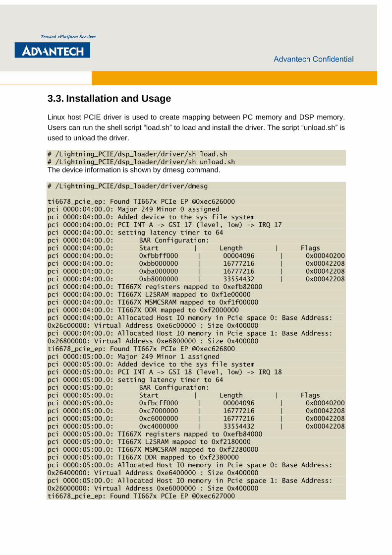
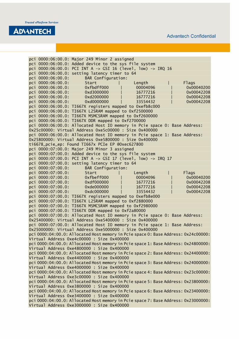
3.3. Installation and Usage
Linux host PCIE driver is used to create mapping between PC memory and DSP memory.
Users can run the shell script “load.sh” to load and install the driver. The script “unload.sh” is
used to unload the driver.
# /Lightning_PCIE/dsp_loader/driver/sh load.sh
# /Lightning_PCIE/dsp_loader/driver/sh unload.sh
The device information is shown by dmesg command.
# /Lightning_PCIE/dsp_loader/driver/dmesg
ti6678_pcie_ep: Found TI667x PCIe EP @0xec626000
pci 0000:04:00.0: Major 249 Minor 0 assigned
pci 0000:04:00.0: Added device to the sys file system
pci 0000:04:00.0: PCI INT A -> GSI 17 (level, low) -> IRQ 17
pci 0000:04:00.0: setting latency timer to 64
pci 0000:04:00.0: BAR Configuration:
pci 0000:04:00.0: Start | Length | Flags
pci 0000:04:00.0: 0xfbbff000 | 00004096 | 0x00040200
pci 0000:04:00.0: 0xbb000000 | 16777216 | 0x00042208
pci 0000:04:00.0: 0xba000000 | 16777216 | 0x00042208
pci 0000:04:00.0: 0xb8000000 | 33554432 | 0x00042208
pci 0000:04:00.0: TI667X registers mapped to 0xefb82000
pci 0000:04:00.0: TI667X L2SRAM mapped to 0xf1e00000
pci 0000:04:00.0: TI667X MSMCSRAM mapped to 0xf1f00000
pci 0000:04:00.0: TI667X DDR mapped to 0xf2000000
pci 0000:04:00.0: Allocated Host IO memory in Pcie space 0: Base Address:
0x26c00000: Virtual Address 0xe6c00000 : Size 0x400000
pci 0000:04:00.0: Allocated Host IO memory in Pcie space 1: Base Address:
0x26800000: Virtual Address 0xe6800000 : Size 0x400000
ti6678_pcie_ep: Found TI667x PCIe EP @0xec626800
pci 0000:05:00.0: Major 249 Minor 1 assigned
pci 0000:05:00.0: Added device to the sys file system
pci 0000:05:00.0: PCI INT A -> GSI 18 (level, low) -> IRQ 18
pci 0000:05:00.0: setting latency timer to 64
pci 0000:05:00.0: BAR Configuration:
pci 0000:05:00.0: Start | Length | Flags
pci 0000:05:00.0: 0xfbcff000 | 00004096 | 0x00040200
pci 0000:05:00.0: 0xc7000000 | 16777216 | 0x00042208
pci 0000:05:00.0: 0xc6000000 | 16777216 | 0x00042208
pci 0000:05:00.0: 0xc4000000 | 33554432 | 0x00042208
pci 0000:05:00.0: TI667X registers mapped to 0xefb84000
pci 0000:05:00.0: TI667X L2SRAM mapped to 0xf2180000
pci 0000:05:00.0: TI667X MSMCSRAM mapped to 0xf2280000
pci 0000:05:00.0: TI667X DDR mapped to 0xf2380000
pci 0000:05:00.0: Allocated Host IO memory in Pcie space 0: Base Address:
0x26400000: Virtual Address 0xe6400000 : Size 0x400000
pci 0000:05:00.0: Allocated Host IO memory in Pcie space 1: Base Address:
0x26000000: Virtual Address 0xe6000000 : Size 0x400000
ti6678_pcie_ep: Found TI667x PCIe EP @0xec627000
pci 0000:06:00.0: Major 249 Minor 2 assigned
pci 0000:06:00.0: Added device to the sys file system
pci 0000:06:00.0: PCI INT A -> GSI 16 (level, low) -> IRQ 16
pci 0000:06:00.0: setting latency timer to 64
pci 0000:06:00.0: BAR Configuration:
pci 0000:06:00.0: Start | Length | Flags
pci 0000:06:00.0: 0xfbdff000 | 00004096 | 0x00040200
pci 0000:06:00.0: 0xd3000000 | 16777216 | 0x00042208
pci 0000:06:00.0: 0xd2000000 | 16777216 | 0x00042208
pci 0000:06:00.0: 0xd0000000 | 33554432 | 0x00042208
pci 0000:06:00.0: TI667X registers mapped to 0xefb8c000
pci 0000:06:00.0: TI667X L2SRAM mapped to 0xf2500000
pci 0000:06:00.0: TI667X MSMCSRAM mapped to 0xf2600000
pci 0000:06:00.0: TI667X DDR mapped to 0xf2700000
pci 0000:06:00.0: Allocated Host IO memory in Pcie space 0: Base Address:
0x25c00000: Virtual Address 0xe5c00000 : Size 0x400000
pci 0000:06:00.0: Allocated Host IO memory in Pcie space 1: Base Address:
0x25800000: Virtual Address 0xe5800000 : Size 0x400000
ti6678_pcie_ep: Found TI667x PCIe EP @0xec627800
pci 0000:07:00.0: Major 249 Minor 3 assigned
pci 0000:07:00.0: Added device to the sys file system
pci 0000:07:00.0: PCI INT A -> GSI 17 (level, low) -> IRQ 17
pci 0000:07:00.0: setting latency timer to 64
pci 0000:07:00.0: BAR Configuration:
pci 0000:07:00.0: Start | Length | Flags
pci 0000:07:00.0: 0xfbeff000 | 00004096 | 0x00040200
pci 0000:07:00.0: 0xdf000000 | 16777216 | 0x00042208
pci 0000:07:00.0: 0xde000000 | 16777216 | 0x00042208
pci 0000:07:00.0: 0xdc000000 | 33554432 | 0x00042208
pci 0000:07:00.0: TI667X registers mapped to 0xefb8e000
pci 0000:07:00.0: TI667X L2SRAM mapped to 0xf2880000
pci 0000:07:00.0: TI667X MSMCSRAM mapped to 0xf2980000
pci 0000:07:00.0: TI667X DDR mapped to 0xf2a80000
pci 0000:07:00.0: Allocated Host IO memory in Pcie space 0: Base Address:
0x25400000: Virtual Address 0xe5400000 : Size 0x400000
pci 0000:07:00.0: Allocated Host IO memory in Pcie space 1: Base Address:
0x25000000: Virtual Address 0xe5000000 : Size 0x400000
pci 0000:04:00.0: Allocated Host memory in Pcie space 0: Base Address: 0x24c00000:
Virtual Address 0xe4c00000 : Size 0x400000
pci 0000:04:00.0: Allocated Host memory in Pcie space 1: Base Address: 0x24800000:
Virtual Address 0xe4800000 : Size 0x400000
pci 0000:04:00.0: Allocated Host memory in Pcie space 2: Base Address: 0x24400000:
Virtual Address 0xe4400000 : Size 0x400000
pci 0000:04:00.0: Allocated Host memory in Pcie space 3: Base Address: 0x24000000:
Virtual Address 0xe4000000 : Size 0x400000
pci 0000:04:00.0: Allocated Host memory in Pcie space 4: Base Address: 0x23c00000:
Virtual Address 0xe3c00000 : Size 0x400000
pci 0000:04:00.0: Allocated Host memory in Pcie space 5: Base Address: 0x23800000:
Virtual Address 0xe3800000 : Size 0x400000
pci 0000:04:00.0: Allocated Host memory in Pcie space 6: Base Address: 0x23400000:
Virtual Address 0xe3400000 : Size 0x400000
pci 0000:04:00.0: Allocated Host memory in Pcie space 7: Base Address: 0x23000000:
Virtual Address 0xe3000000 : Size 0x400000

pci 0000:04:00.0: Allocated Host memory in Pcie space 8: Base Address: 0x22c00000:
Virtual Address 0xe2c00000 : Size 0x400000
pci 0000:04:00.0: Allocated Host memory in Pcie space 9: Base Address: 0x22800000:
Virtual Address 0xe2800000 : Size 0x400000
pci 0000:04:00.0: Allocated Host memory in Pcie space 10: Base Address: 0x22400000:
Virtual Address 0xe2400000 : Size 0x400000
pci 0000:04:00.0: Allocated Host memory in Pcie space 11: Base Address: 0x22000000:
Virtual Address 0xe2000000 : Size 0x400000
pci 0000:04:00.0: Allocated Host memory in Pcie space 12: Base Address: 0x21c00000:
Virtual Address 0xe1c00000 : Size 0x400000
pci 0000:04:00.0: Allocated Host memory in Pcie space 13: Base Address: 0x21800000:
Virtual Address 0xe1800000 : Size 0x400000
pci 0000:04:00.0: Allocated Host memory in Pcie space 14: Base Address: 0x21400000:
Virtual Address 0xe1400000 : Size 0x400000
pci 0000:04:00.0: Allocated Host memory in Pcie space 15: Base Address: 0x21000000:
Virtual Address 0xe1000000 : Size 0x400000
pci 0000:04:00.0: Allocated Host memory in Pcie space 16: Base Address: 0x20c00000:
Virtual Address 0xe0c00000 : Size 0x400000
pci 0000:04:00.0: Allocated Host memory in Pcie space 17: Base Address: 0x20800000:
Virtual Address 0xe0800000 : Size 0x400000
pci 0000:04:00.0: Allocated Host memory in Pcie space 18: Base Address: 0x20400000:
Virtual Address 0xe0400000 : Size 0x400000
pci 0000:04:00.0: Allocated Host memory in Pcie space 19: Base Address: 0x20000000:
Virtual Address 0xe0000000 : Size 0x400000
pci 0000:04:00.0: Allocated Host memory in Pcie space 20: Base Address: 0x1fc00000:
Virtual Address 0xdfc00000 : Size 0x400000
pci 0000:04:00.0: Allocated Host memory in Pcie space 21: Base Address: 0x1f800000:
Virtual Address 0xdf800000 : Size 0x400000
pci 0000:04:00.0: Allocated Host memory in Pcie space 22: Base Address: 0x1f400000:
Virtual Address 0xdf400000 : Size 0x400000
pci 0000:04:00.0: Allocated Host memory in Pcie space 23: Base Address: 0x1f000000:
Virtual Address 0xdf000000 : Size 0x400000
pci 0000:04:00.0: Allocated Host memory in Pcie space 24: Base Address: 0x1ec00000:
Virtual Address 0xdec00000 : Size 0x400000
pci 0000:04:00.0: Allocated Host memory in Pcie space 25: Base Address: 0x1e800000:
Virtual Address 0xde800000 : Size 0x400000
3.4. DSP Loader Utility
DSP loader offers the functions to load the program into DSP memory and notify the DSP to
run program.
3.4.1. Query DSP Information
The command syntax is:
dsp_loader query list or dsp_loader query -l
dsp_loader query [chip#]

The command is to display the PCI information of DSP which are installed in the system. The
more detailed information will be displayed when user specify the [chip#] parameter.
The following two examples demonstrate the result of query command when PC system
install with two Lightning card and query the detailed information of DSP#7.
# /Lightning_PCIE/dsp_loader/app/dsp_loader query list
Card 0:
[Chip 0] Device Name: /dev/ti6678_dsp_0
[Chip 1] Device Name: /dev/ti6678_dsp_1
[Chip 2] Device Name: /dev/ti6678_dsp_2
[Chip 3] Device Name: /dev/ti6678_dsp_3
Card 1:
[Chip 4] Device Name: /dev/ti6678_dsp_4
[Chip 5] Device Name: /dev/ti6678_dsp_5
[Chip 6] Device Name: /dev/ti6678_dsp_6
[Chip 7] Device Name: /dev/ti6678_dsp_7
# /Lightning_PCIE/dsp_loader/app/dsp_loader query 7
==============================================
Chip: 7
Device Name: /dev/ti6678_dsp_7
PCI Bridge from 9 to 14
PCI Bus Num: 14
Vendor ID: 0x0000104c Device ID: 0x0000b005
Class: 0x00000000
Header Type: 0 Irq Pin: 1
BAR Configuration:
Start | Length | Flags
0xf79ff000 | 00004096 | 0x00040200
0xf4000000 | 16777216 | 0x00042208
0xf3000000 | 16777216 | 0x00042208
0xf0000000 | 33554432 | 0x00042208
==============================================
3.4.2. Download DSP Program Image
The command syntax is:
dsp_loader load [chip#] [core#] [image entry point] [image file name (hex)]
The command is to download a DSP program (DSP image) into to RAM of a specified DSP.
The detailed description of each parameter is shown below:
1. [chip#]: the [chip#] are the number of DSPs attached to the PC. Since there are four DSP
devices on the Lightning board, this parameter can be set into 0 ~ 3 for those PC systems
installed with one Lightning card. For those PC systems installed with two Lightning
cards, there will be eight chips available to the PC systems and the parameter can be set
into 0 ~ 7.
2. [core#]: [core#] is used to notify individual core (range from 0 to 7) within DSP to run.
3. [image entry point]: [image entry point] is the start address of the loaded image. User
can find the “entry point symbol” of "_c_int00" in the map file. For example, init.map
information is displayed in List 3-1. The reader can find the entry point of the program in
the top of map file.
******************************************************************************
TMS320C6x Linker PC v7.2.1
******************************************************************************
>> Linked Mon Aug 15 15:03:07 2011
OUTPUT FILE NAME: <../bin/init.out>
ENTRY POINT SYMBOL: "_c_int00" address: 008362a0
List 3-1 entry point in the init.map
4. [image file name]: [image file name] is the full path of hex file name which is loaded into
DSP.
The following example demonstrates how to load /Lightning_PCIE/bin/init.hex (DSP image
for DDR initialization) into DSP#1 and use CPU#0 to run DSP image.
# /Lightning_PCIE/dsp_loader/app/dsp_loader load 1 0 0x008362A0
/Lightning_PCIE/bin/init.hex
Load HEX image: /Lightning_PCIE/bin/init.hex to 1:0, start address 0x008362A0
Load HEX OK
Note: Image entry point depends on DSP image. The image entry point of init.hex (DSP
image) uses address 0x008362A0 as local address for each CPU. Individual local CPU
address can also be transferred to DSP global address with offset. For example, CPU#0 local
address 0x00800000 is equal to DSP global address 0x1080000. CPU#1 local address
0x00800000 is equal to DSP global address 0x1180000.
3.4.3. DSP memory read
The command syntax is:
dsp_loader rmem [chip#] [address]
The command is to read a 32bits-DWORD from DSP. The detailed description of each
parameter is shown below:
1. [chip#]: the [chip#] are the number of DSPs attached to the PC.
2. [address]: read data address
The following example is to read DSP#2 data at address 0x10800000.
# /Lightning_PCIE/dsp_loader/app/dsp_loader rmem 2 0x10800000
0x01bc54f6
3.4.4. DSP memory write
The command syntax is:
dsp_loader load [chip#] [address][value]
The command is to write a 32bits-DWORD into DSP memory. The detailed description of
each parameter is shown below:
1. [chip#]: the [chip#] are the number of DSPs attached to the PC.
2. [address]: written data address
3. [value]: written data
The following example writes data 0x55AA55AA into DSP#2 at address 0x10800000.
# /Lightning_PCIE/dsp_loader/app/dsp_loader wmem 2 0x10800000 0x55aa55aa
# /Lightning_PCIE/dsp_loader/app/dsp_loader rmem 2 0x10800000
0x55aa55aa
3.4.5. Download DSP binary file
The command syntax is:
dsp_loader loadbinary [chip#][address][size][transfer type][bin file name]
The command is to write a bin file into DSP memory. The detailed description of each
parameter is shown below:
1. [chip#]: the [chip#] are the number of DSPs attached to the PC.
2. [address]: written data address
3. [size]: written data size, 0 for all data of file.
4. [transfer type]: 0 for CPU memcpy, 1 for DMA.
5. [bin file name]: [bin file name] is the full path of binary file name which is loaded into
DSP.
The following example writes a jpg file into DSP#1 at DDR beginning address 0x80000000 by
using DMA.
# /Lightning_PCIE/dsp_loader/app/dsp_loader loadbinary 1 0x80000000 0 1
/home/advantech/test_image.jpg
Load Binary file: /home/advantech/test_image.jpg to DSP1, start address
0x80000000, Size 0x00000000
Written to dsp 7496169 bytes
Time measured: 16225 us
Load Binary OK
3.4.6. Save DSP memory as a binary file
The command syntax is:
dsp_loader savebinary [chip#][address][size][transfer type][bin file name]
The command is to read a DSP memory section and save the data as a binary file. The
detailed description of each parameter is shown below:
6. [chip#]: the [chip#] are the number of DSPs attached to the PC.
7. [address]: read data address
8. [size]: read data size
9. [transfer type]: 0 for CPU memcpy, 1 for DMA.
10. [bin file name]: [bin file name] is the full path of binary file name which is saved.
The following example read 7496169 bytes from DSP#1 at DDR beginning address
0x80000000 by using DMA, and saves as test_image_output.jpg.
# /Lightning_PCIE/dsp_loader/app/dsp_loader loadbinary 1 0x80000000 0 1
/home/advantech/test_image.jpg
Load Binary file: /home/advantech/test_image.jpg to DSP1, start address
0x80000000, Size 0x00000000
Written to dsp 7496169 bytes
Time measured: 16225 us
Load Binary OK
# /Lightning_PCIE/dsp_loader/app/dsp_loader savebinary 1 0x80000000 7496169 1
/home/advantech/test_image_output.jpg
Save Binary file: /home/advantech/test_image_output.jpg from DSP 1, start
address 0x80000000 Size 0x007261e9
Saved from dsp 7496169 bytes
Time measured: 21871 us
Save Binary OK
4. Reference Implementations
4.1. Patch of Platform Library and NDK Library
The example programs have to link with TI C6678 platform library and NDK library. A
developer has to install MCSDK first and applies the provided patch. The default path of
MCSDK in Windows is "C:\Program Files\Texas Instruments\".
4.1.1. Build Instruction
Steps to build platform lib are listed below:
1. Patch the modification of TI library, copy all files in
"Lightning_PCIE\patch\pdk_C6678_1_0_0_21" and paste to "C:\Program Files\Texas
Instruments\pdk_C6678_1_0_0_21"
2. Import the CCS project from
"pdk_C6678_1_0_0_21\packages\ti\platform\evmc6678l\platform_lib" directory (in
CCSv5, Project->Import Existing CCS/CCE Eclipse Projects)
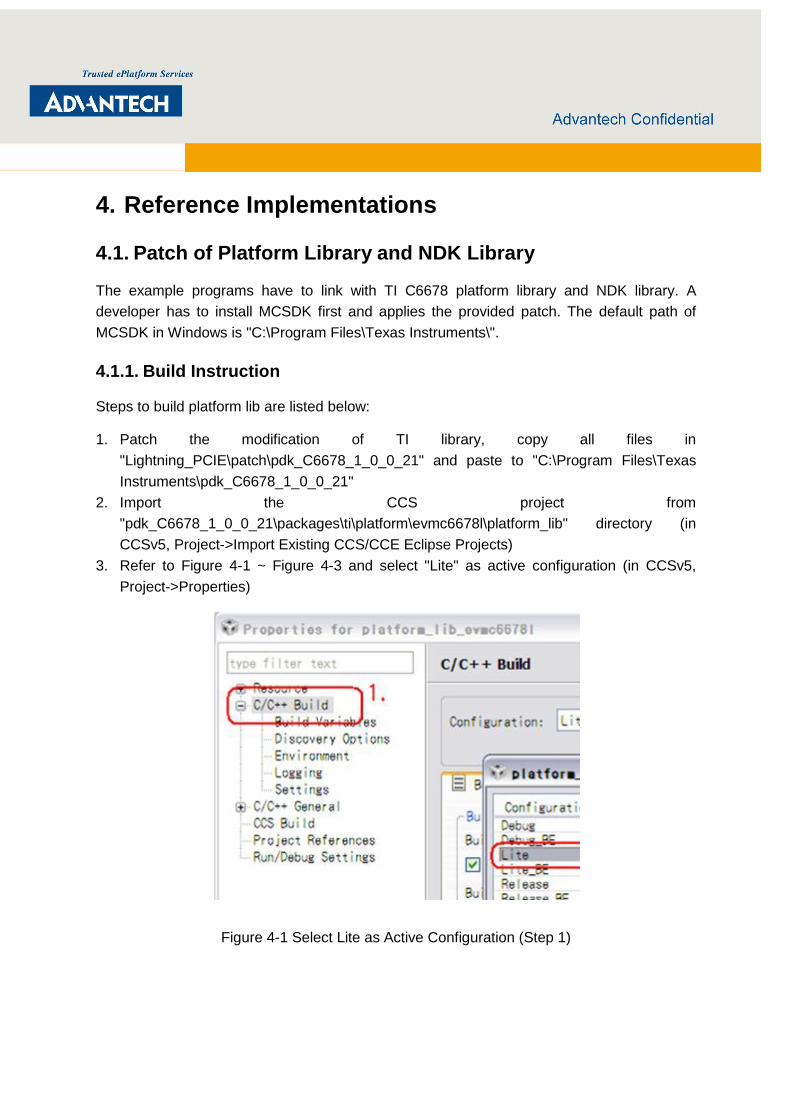
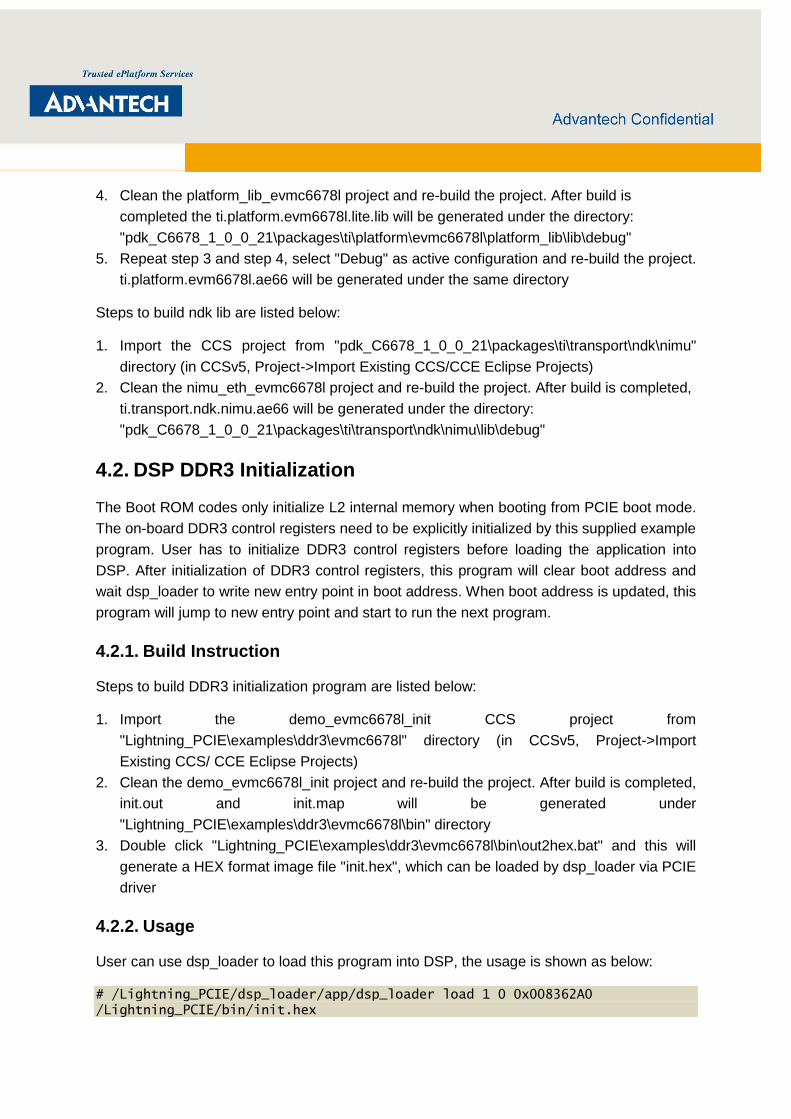
3. Refer to Figure 4-1 ~ Figure 4-3 and select "Lite" as active configuration (in CCSv5,
Project->Properties)
Figure 4-1 Select Lite as Active Configuration (Step 1)
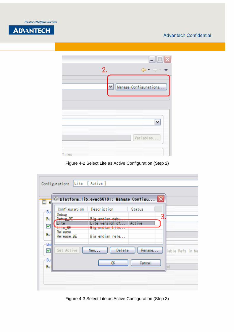
Figure 4-2 Select Lite as Active Configuration (Step 2)
Figure 4-3 Select Lite as Active Configuration (Step 3)
4. Clean the platform_lib_evmc6678l project and re-build the project. After build is
completed the ti.platform.evm6678l.lite.lib will be generated under the directory:
"pdk_C6678_1_0_0_21\packages\ti\platform\evmc6678l\platform_lib\lib\debug"
5. Repeat step 3 and step 4, select "Debug" as active configuration and re-build the project.
ti.platform.evm6678l.ae66 will be generated under the same directory
Steps to build ndk lib are listed below:
1. Import the CCS project from "pdk_C6678_1_0_0_21\packages\ti\transport\ndk\nimu"
directory (in CCSv5, Project->Import Existing CCS/CCE Eclipse Projects)
2. Clean the nimu_eth_evmc6678l project and re-build the project. After build is completed,
ti.transport.ndk.nimu.ae66 will be generated under the directory:
"pdk_C6678_1_0_0_21\packages\ti\transport\ndk\nimu\lib\debug"
4.2. DSP DDR3 Initialization
The Boot ROM codes only initialize L2 internal memory when booting from PCIE boot mode.
The on-board DDR3 control registers need to be explicitly initialized by this supplied example
program. User has to initialize DDR3 control registers before loading the application into
DSP. After initialization of DDR3 control registers, this program will clear boot address and
wait dsp_loader to write new entry point in boot address. When boot address is updated, this
program will jump to new entry point and start to run the next program.
4.2.1. Build Instruction
Steps to build DDR3 initialization program are listed below:
1. Import the demo_evmc6678l_init CCS project from
"Lightning_PCIE\examples\ddr3\evmc6678l" directory (in CCSv5, Project->Import
Existing CCS/ CCE Eclipse Projects)
2. Clean the demo_evmc6678l_init project and re-build the project. After build is completed,
init.out and init.map will be generated under
"Lightning_PCIE\examples\ddr3\evmc6678l\bin" directory
3. Double click "Lightning_PCIE\examples\ddr3\evmc6678l\bin\out2hex.bat" and this will
generate a HEX format image file "init.hex", which can be loaded by dsp_loader via PCIE
driver
4.2.2. Usage
User can use dsp_loader to load this program into DSP, the usage is shown as below:
# /Lightning_PCIE/dsp_loader/app/dsp_loader load 1 0 0x008362A0
/Lightning_PCIE/bin/init.hex
Load HEX image: /Lightning_PCIE/bin/init.hex to 1:0, start address 0x008362A0
Load HEX OK
Refer to 4.3.2 for usage of Ethernet example, which illustrates how to use DDR3 initialization
program to initialize DDR3 and then load Ethernet program into DDR3.
4.3. Ethernet and Simple Web Server
The Ethernet program is modified from the example codes in TI MCSDK. This example
implements a simple web server running on DSP. The Ethernet port on the bracket of the
Lightning board must be connected to an external Ethernet switch (support gigabit rate)
before running this example. Each DSP has a fixed IP number that is determined by its order.
The pre-given IP addresses are shown below. The user can use a browser to view the simple
web page provided by this simple web server.
IP
DSP 0 192.168.1.101
DSP 1 192.168.1.102
DSP 2 192.168.1.103
DSP 3 192.168.1.104
4.3.1. Build Instruction
Steps to build web server program are listed below:
1. Import the client_evmc6678l CCS project from
"Lightning_PCIE\examples\web\client\evmc6678l" directory (in CCSv5, Project->Import
Existing CCS/ CCE Eclipse Projects)
2. Select DSPC8681E as active configuration.
3. Clean the client_evmc6678l project and re-build the project. After build is completed,
client_evmc6678l.out and client_evmc6678l.map will be generated under
"Lightning_PCIE\examples\web\client\evmc6678l\DSPC8681E" directory
4. Double click "Lightning_PCIE\examples\web\client\evmc6678l\DSPC8681E\out2hex.bat"
and this will generate a HEX format image file "client_evmc6678l.hex", which can be
loaded by dsp_loader via PCIE driver
4.3.2. Usage
User can use the shell script "Lightning_PCIE/examples/script/DSPC8681E/ethernet.sh" to
setup Ethernet program on each DSP automatically or follow the steps to set up manually.
1. Load the driver
# /Lightning_PCIE/dsp_loader/driver/sh load.sh
2. Load init.hex into each DSP to initialize the DDR3.
# /Lightning_PCIE/dsp_loader/app/dsp_loader load 0 0 0x008362A0
/Lightning_PCIE/bin/init.hex
# /Lightning_PCIE/dsp_loader/app/dsp_loader load 1 0 0x008362A0
/Lightning_PCIE/bin/init.hex
# /Lightning_PCIE/dsp_loader/app/dsp_loader load 2 0 0x008362A0
/Lightning_PCIE/bin/init.hex
# /Lightning_PCIE/dsp_loader/app/dsp_loader load 3 0 0x008362A0
/Lightning_PCIE/bin/init.hex
3. Load network client into each DSP.
# /Lightning_PCIE/dsp_loader/app/dsp_loader load 0 0 0x800714e0
/Lightning_PCIE/bin/client_evmc6678l.hex
# /Lightning_PCIE/dsp_loader/app/dsp_loader load 1 0 0x800714e0
/Lightning_PCIE/bin/client_evmc6678l.hex
# /Lightning_PCIE/dsp_loader/app/dsp_loader load 2 0 0x800714e0
/Lightning_PCIE/bin/client_evmc6678l.hex
# /Lightning_PCIE/dsp_loader/app/dsp_loader load 3 0 0x800714e0
/Lightning_PCIE/bin/client_evmc6678l.hex
4. Check the result by internet browser. The URL of DSPs are http://192.168.1.10X, X=1~4.
The result is shown in Figure 4-4 and Figure 4-5.

Figure 4-4 TCP/IP Demo Page
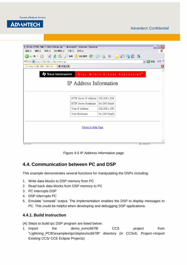
Figure 4-5 IP Address Information page
4.4. Communication between PC and DSP
This example demonstrates several functions for manipulating the DSPs including:
1. Write data blocks to DSP memory from PC
2. Read back data blocks from DSP memory to PC
3. PC interrupts DSP
4. DSP interrupts PC
5. Emulate “console” output. The implementation enables the DSP to display messages to
PC. This could be helpful when developing and debugging DSP applications.
4.4.1. Build Instruction
(A) Steps to build ipc DSP program are listed below:
1. Import the demo_evmc6678l CCS project from
"Lightning_PCIE\examples\ipc\dsp\evmc6678l" directory (in CCSv5, Project->Import
Existing CCS/ CCE Eclipse Projects)
2. Select DSPC8681E as active configuration.
3. Clean the demo_evmc6678l project and re-build the project. After build is completed,
demo_evm6678l.out and demo_evm6678l.map will be generated under
"Lightning_PCIE\examples\ipc\dsp\evmc6678l\bin" directory
4. Double click "Lightning_PCIE\examples\ipc\dsp\evmc6678l\bin\out2hex.bat" and this will
generate a HEX format image file "demo_evm6678l.hex", which can be loaded by
dsp_loader via PCIE driver
(B) Build ipc PC utility:
User can use this command to build PC utility:
# /Lightning_PCIE/examples/ipc/pc/make clean
# /Lightning_PCIE/examples/ipc/pc/make
dsp_demo will be generated in the same directory.
4.4.2. Usage
User can use shell script file "Lightning_PCIE/examples/script/DSPC8681E/ipc.sh" to load
demo_evm6678l.hex into the specific DSP.
The demo command is used to display the negotiation between DSP and PC host. dsp_demo
will wait the interrupt signal which is sent from PCIe driver and perform the data blocks
read/write. [chip#] (From DSP#0 to DSP#3) parameter selects which DSP will be accessed
by PC.
The command syntax is:
dsp_demo demo [chip#]
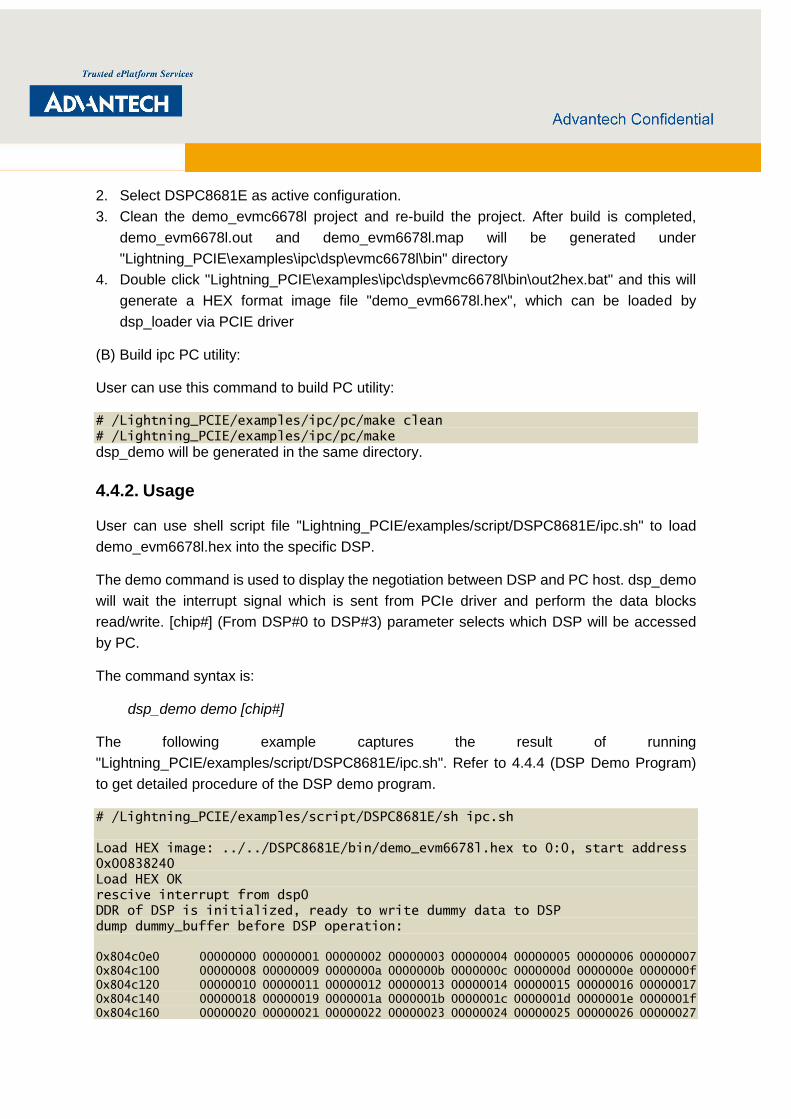
The following example captures the result of running
"Lightning_PCIE/examples/script/DSPC8681E/ipc.sh". Refer to 4.4.4 (DSP Demo Program)
to get detailed procedure of the DSP demo program.
# /Lightning_PCIE/examples/script/DSPC8681E/sh ipc.sh
Load HEX image: ../../DSPC8681E/bin/demo_evm6678l.hex to 0:0, start address
0x00838240
Load HEX OK
rescive interrupt from dsp0
DDR of DSP is initialized, ready to write dummy data to DSP
dump dummy_buffer before DSP operation:
0x804c0e0 00000000 00000001 00000002 00000003 00000004 00000005 00000006 00000007
0x804c100 00000008 00000009 0000000a 0000000b 0000000c 0000000d 0000000e 0000000f
0x804c120 00000010 00000011 00000012 00000013 00000014 00000015 00000016 00000017
0x804c140 00000018 00000019 0000001a 0000001b 0000001c 0000001d 0000001e 0000001f
0x804c160 00000020 00000021 00000022 00000023 00000024 00000025 00000026 00000027
0x804c180 00000028 00000029 0000002a 0000002b 0000002c 0000002d 0000002e 0000002f
0x804c1a0 00000030 00000031 00000032 00000033 00000034 00000035 00000036 00000037
0x804c1c0 00000038 00000039 0000003a 0000003b 0000003c 0000003d 0000003e 0000003f
0x804c1e0 00000040 00000041 00000042 00000043 00000044 00000045 00000046 00000047
0x804c200 00000048 00000049 0000004a 0000004b 0000004c 0000004d 0000004e 0000004f
0x804c220 00000050 00000051 00000052 00000053 00000054 00000055 00000056 00000057
0x804c240 00000058 00000059 0000005a 0000005b 0000005c 0000005d 0000005e 0000005f
0x804c260 00000060 00000061 00000062 00000063 00000064 00000065 00000066 00000067
0x804c280 00000068 00000069 0000006a 0000006b 0000006c 0000006d 0000006e 0000006f
0x804c2a0 00000070 00000071 00000072 00000073 00000074 00000075 00000076 00000077
0x804c2c0 00000078 00000079 0000007a 0000007b 0000007c 0000007d 0000007e 0000007f
0x804c2e0 00000080 00000081 00000082 00000083 00000084 00000085 00000086 00000087
0x804c300 00000088 00000089 0000008a 0000008b 0000008c 0000008d 0000008e 0000008f
0x804c320 00000090 00000091 00000092 00000093 00000094 00000095 00000096 00000097
0x804c340 00000098 00000099 0000009a 0000009b 0000009c 0000009d 0000009e 0000009f
rescive interrupt from dsp0
dummy data has already been changed by DSP
dump dummy_buffer after DSP operation:
0x804c0e0 00000001 00000002 00000003 00000004 00000005 00000006 00000007 00000008
0x804c100 00000009 0000000a 0000000b 0000000c 0000000d 0000000e 0000000f 00000010
0x804c120 00000011 00000012 00000013 00000014 00000015 00000016 00000017 00000018
0x804c140 00000019 0000001a 0000001b 0000001c 0000001d 0000001e 0000001f 00000020
0x804c160 00000021 00000022 00000023 00000024 00000025 00000026 00000027 00000028
0x804c180 00000029 0000002a 0000002b 0000002c 0000002d 0000002e 0000002f 00000030
0x804c1a0 00000031 00000032 00000033 00000034 00000035 00000036 00000037 00000038
0x804c1c0 00000039 0000003a 0000003b 0000003c 0000003d 0000003e 0000003f 00000040
0x804c1e0 00000041 00000042 00000043 00000044 00000045 00000046 00000047 00000048
0x804c200 00000049 0000004a 0000004b 0000004c 0000004d 0000004e 0000004f 00000050
0x804c220 00000051 00000052 00000053 00000054 00000055 00000056 00000057 00000058
0x804c240 00000059 0000005a 0000005b 0000005c 0000005d 0000005e 0000005f 00000060
0x804c260 00000061 00000062 00000063 00000064 00000065 00000066 00000067 00000068
0x804c280 00000069 0000006a 0000006b 0000006c 0000006d 0000006e 0000006f 00000070
0x804c2a0 00000071 00000072 00000073 00000074 00000075 00000076 00000077 00000078
0x804c2c0 00000079 0000007a 0000007b 0000007c 0000007d 0000007e 0000007f 00000080
0x804c2e0 00000081 00000082 00000083 00000084 00000085 00000086 00000087 00000088
0x804c300 00000089 0000008a 0000008b 0000008c 0000008d 0000008e 0000008f 00000090
0x804c320 00000091 00000092 00000093 00000094 00000095 00000096 00000097 00000098
0x804c340 00000099 0000009a 0000009b 0000009c 0000009d 0000009e 0000009f 000000a0
4.4.3. Console Simulation
This command is for creating a virtual console to display the debug message by the program
running in specific DSP (chip# from DSP#0 to DSP#3) and cores (core# from CPU core#0 to
CPU core#7).
The command syntax is:
dsp_demo console [chip#] [core#]
The following example displays the debug message of demo_evm6678l.hex (DSP demo
program) which is executed by CPU#0 in DSP#0.
# /Lightning_PCIE/examples/ipc/pc/dsp_demo console 0 0
Synchronizing ... done.
===========================
PCIe Hello World Example, this is DSP0
Debug: GEM-INTC Configuration Completed
Debug: CPINTC-0 Configuration...
Debug: CPINTC-0 Configuration Completed
DSP0 generated interrupt to host
DSP0 receive interrupt from host
DSP0 finish operating dummy data.
Note: DSP program demo_evm6678l.hex should be downloaded to DSP device first before
issuing this virtual console command. Refer to the source code of DSP demo program to get
detailed implementation.
4.4.4. DSP Demo Program
DSP demo program initializes DDR control registers and configures DSP INTC to receive
PCIE interrupt from PC host. The procedure of demo program is illustrated below with flow
chart displayed in Figure 4-6:
1. Initialize PLL, DDR, ECC and UART, set up INTC for ISR handler and then send an
interrupt to PC host
2. PC host writes test data pattern whose length is 640-byte to DSP DDR and sends an
interrupt to DSP after finishing the writing of the test data pattern
3. The test data pattern in DDR will be added by 1 when DSP receives the interrupt from PC
host. After finishing the operation, DSP will send an interrupt back to PC host.
4. PC Host receives the interrupt from DSP as the indication that the test data pattern has
already been changed and prints the test data pattern
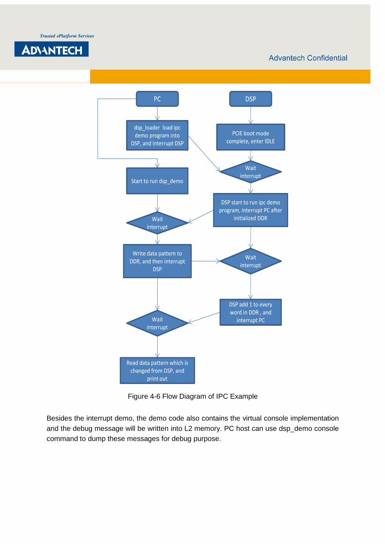
Figure 4-6 Flow Diagram of IPC Example
Besides the interrupt demo, the demo code also contains the virtual console implementation
and the debug message will be written into L2 memory. PC host can use dsp_demo console
command to dump these messages for debug purpose.

4.5. Image Processing Demonstration
The image processing program is modified from the example codes in TI MCSDK. This
application shows implementation of an image processing system using a simple multicore
framework. This application will run TI image processing kernels (imagelib) on multiple cores
to do image processing (eg: edge detection, etc) on an input image.
Figure 4-7 Image Processing Application Software Framework
The user input image will be BMP image. The image will be transferred to external memory
using NDK (http). The Ethernet port on the bracket of the Lightning board must be connected
to an external Ethernet switch (support gigabit rates) before running this example. Each DSP
has a fixed IP number that is determined by its order. The pre-given IP addresses are shown
below. The user can use a browser to input the BMP image form web page provided by HTTP
server.
IP
DSP 0 192.168.1.101
DSP 1 192.168.1.102
DSP 2 192.168.1.103
DSP 3 192.168.1.104
PC Setting
IP 192.168.1.100
Subnet Mask 255.255.254.0
4.5.1. Build Instruction
Steps to build image processing program are listed below:
1. Import the client_evmc6678l CCS project from
"Lightning_PCIE\examples\image_processing\ipc\evmc6678l" directory (in CCSv5,
Project->Import Existing CCS/ CCE Eclipse Projects)
2. Select DSPC8681E as active configuration.
3. Clean the image_processing_evmc6678l_master project and re-build the project. After
build is completed, image_processing_evmc6678l_master.out will be generated under
the directory:
"Lightning_PCIE\examples\image_processing\ipc\evmc6678l\master\DSPC8681E"
4. Clean the image_processing_evmc6678l_slave project and re-build the project. After
build is completed, image_processing_evmc6678l_slave.out will be generated under the
directory: "Lightning_PCIE\examples\image_processing\ipc\evmc6678l\slave\Debug"
5. Double click
"Lightning_PCIE\examples\image_processing\ipc\evmc6678l\master\DSPC8681E\out2h
ex.bat" and this will generate a HEX format image file "
image_processing_evmc6678l_master.hex", which can be loaded by dsp_loader via
PCIE driver
6. Double click "Lightning_PCIE\examples\image_processing\ipc\evmc6678l\slave\Debug
\out2hex.bat" and this will generate a HEX format image file "
image_processing_evmc6678l_slave.hex", which can be loaded by dsp_loader via PCIE
driver
4.5.2. Usage
User can use the shell script
"Lightning_PCIE/examples/script/DSPC8681E/image_processing.sh" to setup image
processing program on each DSP automatically or follow the steps to set up manually.
1. Load the driver
# /Lightning_PCIE/dsp_loader/driver/sh image_processing.sh
2. Load init.hex into core0 of each DSP to initialize the DDR3.
# /Lightning_PCIE/dsp_loader/app/dsp_loader load 0 0 0x00836320
/Lightning_PCIE/bin/init.hex
# /Lightning_PCIE/dsp_loader/app/dsp_loader load 1 0 0x00836320
/Lightning_PCIE/bin/init.hex
# /Lightning_PCIE/dsp_loader/app/dsp_loader load 2 0 0x00836320
/Lightning_PCIE/bin/init.hex
# /Lightning_PCIE/dsp_loader/app/dsp_loader load 3 0 0x00836320
/Lightning_PCIE/bin/init.hex
3. Load image processing slave into core1~core7 of each DSP.
# /Lightning_PCIE/dsp_loader/app/dsp_loader load 0 1 0x0c12dfa0
/Lightning_PCIE/bin/image_processing_evmc6678l_slave.hex
# /Lightning_PCIE/dsp_loader/app/dsp_loader load 0 2 0x0c12dfa0
/Lightning_PCIE/bin/image_processing_evmc6678l_slave.hex
# /Lightning_PCIE/dsp_loader/app/dsp_loader load 0 3 0x0c12dfa0
/Lightning_PCIE/bin/image_processing_evmc6678l_slave.hex
# /Lightning_PCIE/dsp_loader/app/dsp_loader load 0 4 0x0c12dfa0
/Lightning_PCIE/bin/image_processing_evmc6678l_slave.hex
# /Lightning_PCIE/dsp_loader/app/dsp_loader load 0 5 0x0c12dfa0
/Lightning_PCIE/bin/image_processing_evmc6678l_slave.hex
# /Lightning_PCIE/dsp_loader/app/dsp_loader load 0 6 0x0c12dfa0
/Lightning_PCIE/bin/image_processing_evmc6678l_slave.hex
# /Lightning_PCIE/dsp_loader/app/dsp_loader load 0 7 0x0c12dfa0
/Lightning_PCIE/bin/image_processing_evmc6678l_slave.hex
# /Lightning_PCIE/dsp_loader/app/dsp_loader load 1 1 0x0c12dfa0
/Lightning_PCIE/bin/image_processing_evmc6678l_slave.hex
# /Lightning_PCIE/dsp_loader/app/dsp_loader load 1 2 0x0c12dfa0
/Lightning_PCIE/bin/image_processing_evmc6678l_slave.hex
# /Lightning_PCIE/dsp_loader/app/dsp_loader load 1 3 0x0c12dfa0
/Lightning_PCIE/bin/image_processing_evmc6678l_slave.hex
# /Lightning_PCIE/dsp_loader/app/dsp_loader load 1 4 0x0c12dfa0
/Lightning_PCIE/bin/image_processing_evmc6678l_slave.hex
# /Lightning_PCIE/dsp_loader/app/dsp_loader load 1 5 0x0c12dfa0
/Lightning_PCIE/bin/image_processing_evmc6678l_slave.hex
# /Lightning_PCIE/dsp_loader/app/dsp_loader load 1 6 0x0c12dfa0
/Lightning_PCIE/bin/image_processing_evmc6678l_slave.hex
# /Lightning_PCIE/dsp_loader/app/dsp_loader load 1 7 0x0c12dfa0
/Lightning_PCIE/bin/image_processing_evmc6678l_slave.hex
# /Lightning_PCIE/dsp_loader/app/dsp_loader load 2 1 0x0c12dfa0
/Lightning_PCIE/bin/image_processing_evmc6678l_slave.hex
# /Lightning_PCIE/dsp_loader/app/dsp_loader load 2 2 0x0c12dfa0
/Lightning_PCIE/bin/image_processing_evmc6678l_slave.hex
# /Lightning_PCIE/dsp_loader/app/dsp_loader load 2 3 0x0c12dfa0
/Lightning_PCIE/bin/image_processing_evmc6678l_slave.hex
# /Lightning_PCIE/dsp_loader/app/dsp_loader load 2 4 0x0c12dfa0
/Lightning_PCIE/bin/image_processing_evmc6678l_slave.hex
# /Lightning_PCIE/dsp_loader/app/dsp_loader load 2 5 0x0c12dfa0
/Lightning_PCIE/bin/image_processing_evmc6678l_slave.hex
# /Lightning_PCIE/dsp_loader/app/dsp_loader load 2 6 0x0c12dfa0
/Lightning_PCIE/bin/image_processing_evmc6678l_slave.hex
# /Lightning_PCIE/dsp_loader/app/dsp_loader load 2 7 0x0c12dfa0
/Lightning_PCIE/bin/image_processing_evmc6678l_slave.hex
# /Lightning_PCIE/dsp_loader/app/dsp_loader load 3 1 0x0c12dfa0
/Lightning_PCIE/bin/image_processing_evmc6678l_slave.hex
# /Lightning_PCIE/dsp_loader/app/dsp_loader load 3 2 0x0c12dfa0
/Lightning_PCIE/bin/image_processing_evmc6678l_slave.hex
# /Lightning_PCIE/dsp_loader/app/dsp_loader load 3 3 0x0c12dfa0
/Lightning_PCIE/bin/image_processing_evmc6678l_slave.hex
# /Lightning_PCIE/dsp_loader/app/dsp_loader load 3 4 0x0c12dfa0
/Lightning_PCIE/bin/image_processing_evmc6678l_slave.hex
# /Lightning_PCIE/dsp_loader/app/dsp_loader load 3 5 0x0c12dfa0
/Lightning_PCIE/bin/image_processing_evmc6678l_slave.hex
# /Lightning_PCIE/dsp_loader/app/dsp_loader load 3 6 0x0c12dfa0
/Lightning_PCIE/bin/image_processing_evmc6678l_slave.hex
# /Lightning_PCIE/dsp_loader/app/dsp_loader load 3 7 0x0c12dfa0
/Lightning_PCIE/bin/image_processing_evmc6678l_slave.hex
4. Load image processing master into core0 of each DSP.
# /Lightning_PCIE/dsp_loader/app/dsp_loader load 0 0 0x0c072ea0
/Lightning_PCIE/bin/image_processing_evmc6678l_master.hex
# /Lightning_PCIE/dsp_loader/app/dsp_loader load 1 0 0x0c072ea0
/Lightning_PCIE/bin/image_processing_evmc6678l_master.hex
# /Lightning_PCIE/dsp_loader/app/dsp_loader load 2 0 0x0c072ea0
/Lightning_PCIE/bin/image_processing_evmc6678l_master.hex
# /Lightning_PCIE/dsp_loader/app/dsp_loader load 3 0 0x0c072ea0
/Lightning_PCIE/bin/image_processing_evmc6678l_master.hex
5. Please refer to the Figure 4-8. Input the BMP image form the internet browser. The URL
of DSPs are http://192.168.1.10X, X=1~4. Select the number of core and image path for
processing.
6. The output result is shown in Figure 4-9.
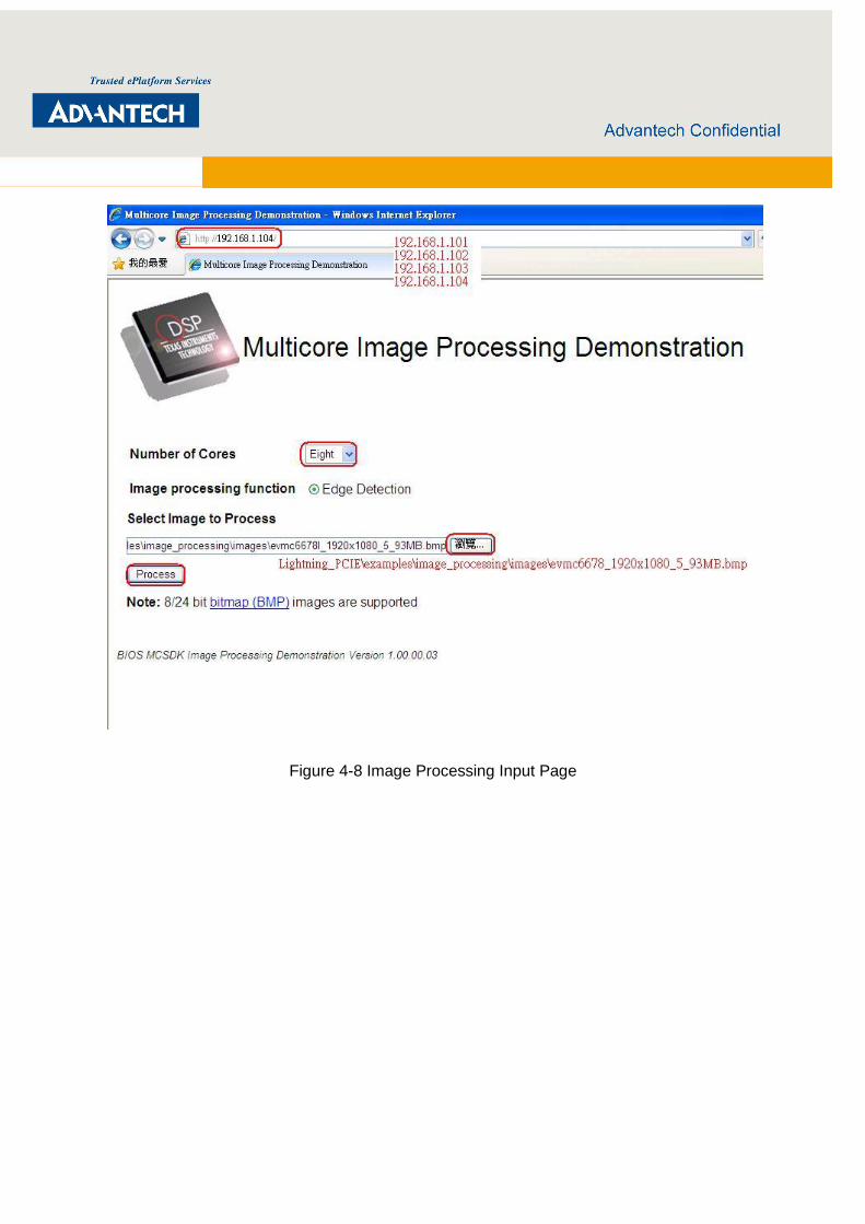
Figure 4-8 Image Processing Input Page
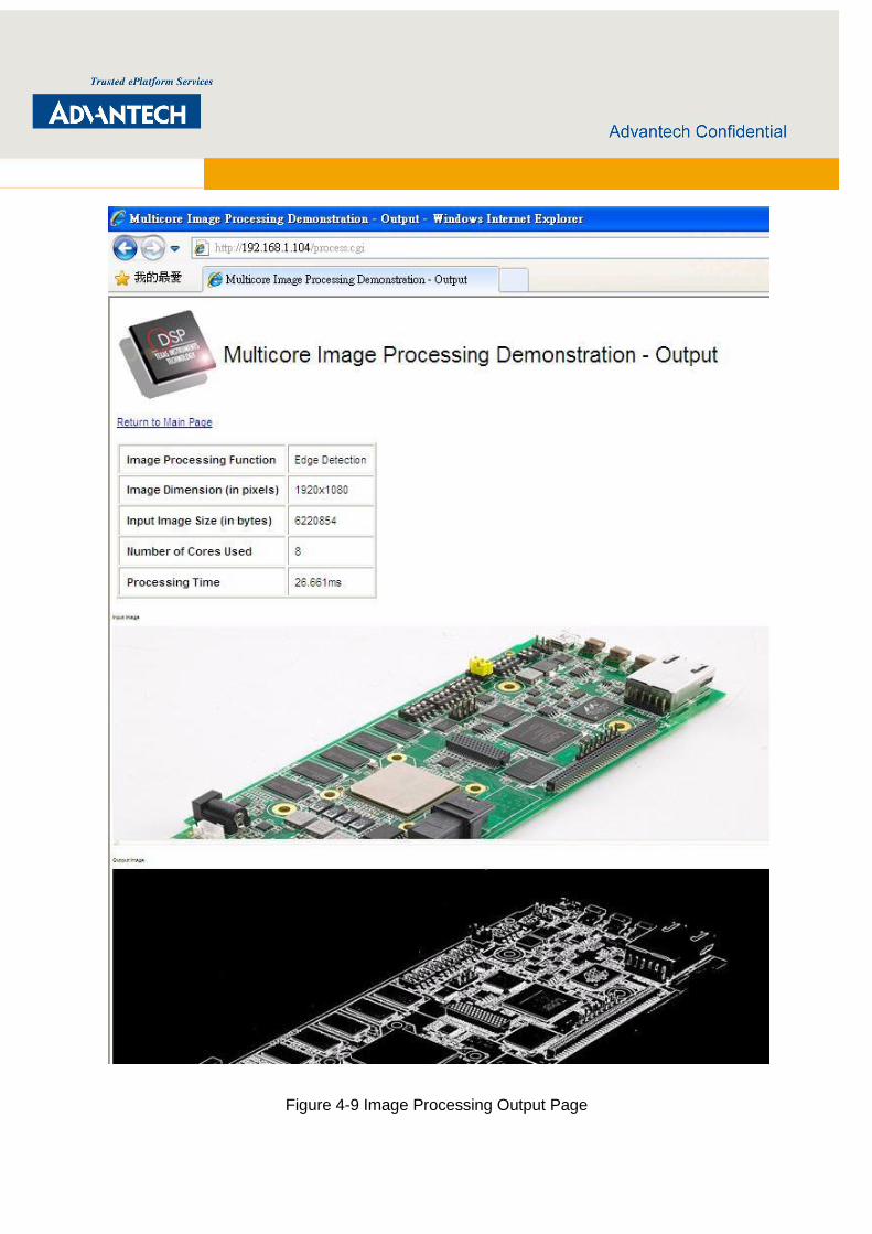
Figure 4-9 Image Processing Output Page