Light Conversion and Transmission Studies for the NEXT Experiment
78
Light Conversion and Transmission Studies for the NEXT Experiment José Miguel de Carvalho Amaral Garcia Master Universitari en Física Médica Universitat de València Instituto de Física Corpuscular July 2014 Supervisor: Dr. Nadia Yahlali
-
Upload
nguyendang -
Category
Documents
-
view
222 -
download
0
Transcript of Light Conversion and Transmission Studies for the NEXT Experiment
Light Conversion and Transmission
Studies for
the NEXT Experiment
José Miguel de Carvalho Amaral Garcia
Master Universitari en Física Médica
Universitat de València
Instituto de Física Corpuscular
July 2014
Supervisor: Dr. Nadia Yahlali


Acknowledgments
First of all, I want to thank my supervisor Dr. Nadia Yahlali who guided me
during this thesis and all the work that preceded it, for teaching me how to work in the
lab and for supporting me all the time. A special thank to Professor José Díaz for
giving me the opportunity to work at IFIC and for making possible my beginning in the
world of experimental Physics. Thank to both for all the patience and personal
advices. I would like to thank the whole NEXT collaboration, especially Andrew Laing,
Justo Martin-Albo and Paola Ferrario, for their help and support whenever was
needed. I also thank Henk Bolink, Alejandra Soriano and Angel López, from ICMOL,
for their availability when needed and the help provided with the tests made at their
laboratory.
I acknowledge a grant from Santiago Grisolía program for research staff
training in research centers of the Valencian Community.
A special thank to my brother Alexandre Garcia for giving me the opportunity of
knowing the NEXT experiment that made possible my involvement and contribution. I
would like to thank all my family, mainly Alexandre, my sister Sofia, and my parents,
Isabel and José Alberto, for all their patience, support, advices, and the efforts made
during all this years that gave me the opportunity of my accomplishments. I would like
to thank Nanci for all the support that she provided me and for all her comprehension.
Finally, mentioning that the distance is required but you are always near.
Thank you very much!

Contents
Chapter 1
The NEXT Experiment .......................................................................... 7
1.1. Introduction ....................................................................................................... 7
1.2. The NEXT-100 experiment .............................................................................. 10
1.2.1. Design concepts................................................................................ 10
1.2.2. Projected sensitivity ......................................................................... 12
1.3. NEXT-DEMO .................................................................................................... 14
1.4. NEXT-WHITE (NEW) ........................................................................................ 18
1.5. This Master Thesis .......................................................................................... 20
Chapter 2
Light conversion studies ................................................................... 21
2.1. Measurements of SiPMs Photo-detection Efficiency ................................... 22
2.1.1. Measurement principle ......................................................................... 22
2.1.2. Experimental Setup .............................................................................. 25
2.1.3. Results and Conclusions ..................................................................... 28
2.2. Measurement of TPB Quantum Efficiency .................................................... 30
2.2.1. Evaporated TPB coatings .................................................................... 31
2.2.2. TPB-PS mixture coatings ..................................................................... 33
2.2.3. QE measurement principle .................................................................. 35
2.2.4. Experimental setup ............................................................................... 37
2.2.5. Results and Conclusions ..................................................................... 40
Chapter 3
Light transmission studies ................................................................ 47
3.1. Conductive and transparent coatings in NEW ............................................. 47
3.1.1. Transparent Materials for Windows ..................................................... 48
3.1.2. Transparent and Conductive Coatings ............................................... 49
3.1.3. Experimental Setup for transmittance measurement ........................ 51
3.1.4. Results and Conclusions ..................................................................... 52
3.2. Light transmission in NEW PMT Cans .......................................................... 57
3.2.1. Optical coupling and Transmittance curves ....................................... 57
3.2.2. Experimental Setup............................................................................... 60
3.2.3. Simulations ............................................................................................ 61
3.2.4. Results and Conclusions ..................................................................... 62
Chapter 4
Summary and General Conclusions .................................................. 65
Chapter 5
Possible applications in Medical Physics ......................................... 69
Bibliography ............................................................................................................ 71
Acronyms Index ...................................................................................................... 75
Abstract
As a contribution to NEXT-100 (Neutrino Experiment with a Xenon Time Projection
Chamber (TPC)) experiment, we performed several studies aiming at improving the
detection of the xenon scintillation in the TPC. In this Master thesis we present the
measurements of the Photon Detection Efficiency (PDE) of Silicon Photomultipliers
(SiPMs) coated and non-coated with the wavelength shifter TPB (Tetraphenyl
Butadiene), the Quantum Efficiency (QE) of the TPB, the transmittance of conductive
and transparent coatings, and the optimization of the light transmission to the PMTs
(Photomultiplier) of the energy plane using an optical coupling between the PMT
quartz window and the sapphire window of the PMTs enclosures. These
measurements were performed in NEXT laboratory at IFIC and at ICMOL. The main
results are presented and the improvements are outlined.

7
Chapter 1
The NEXT Experiment
1.1. Introduction
The Neutrino () is an electrically neutral, weakly interacting elementary
subatomic particle [1] created in the radioactive decay of nuclei including the emission
of a beta particle (electron or positron). When the beta decay occurs the atom obtains
a more stable nucleus because it attains an optimum ratio of protons and neutrons,
since a proton converts into a neutron, or vice-versa, and the nucleus emits an
electron (the beta minus, -) or a positron (the beta plus, +) and one neutrino or
antineutrino ( .
The - decay is a process in which an atomic nucleus (A, Z) is converted to
other with a higher atomic number (A, Z+1), i.e., a neutron (n) decays into a proton
(p), with the emission of an electron (e-) and an electron antineutrino ( ):
( ( ( 1 )
In opposition to the previous, in the + decay the (A, Z) nucleus is converted
into a (A, Z−1) nucleus, that is, a proton decays into a neutron, with is the emission of
a positron and an electron neutrino ( ):
( ( ( 2 )
There is also possibility to have electron capture when the + decay happens.
In this case, the same nucleus captures one electron that orbits around the atom to
obtain a neutron, emitting a neutrino:
( ( ( 3 )
8
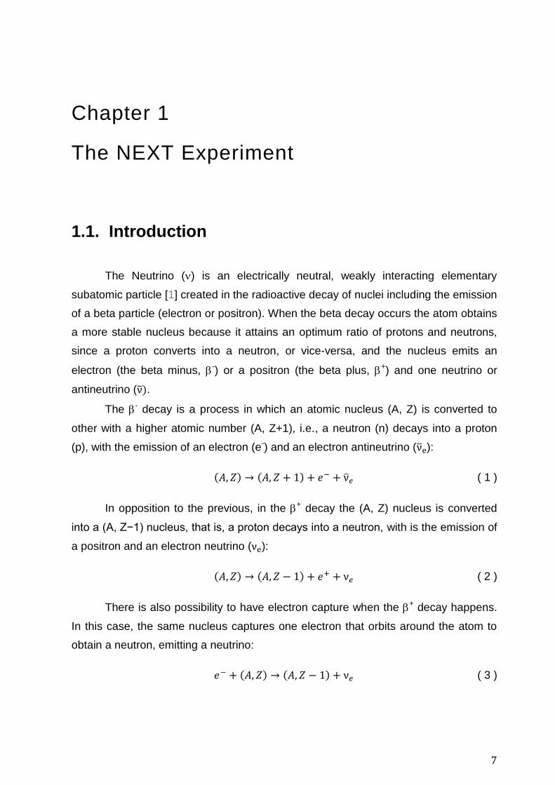
Another decay process that may occur with emission of neutrinos is the
double-beta decay (2). This process can only be observed if the simple beta
decay doesn’t occur because it is energetically forbidden [2] (figure 1). This is why it
has a much smaller probability to occur and is experimentally observed only for some
isotopes among them the 136Xe. The two-neutrino double beta decay (2) is a sum
of two - decays, in which two neutrons in the nuclei are converted in two protons,
with the emission of two electrons and two electron antineutrinos:
( ( ( 4 )
As demonstrated theoretically by Ettore Majorana in 1937, if the neutrino is its
own antiparticle, i.e., if it is a Majorana particle, the double beta decay can occur
without the emission of any neutrino, the so-called neutrinoless double beta decay
(0):
( ( ( 5 )
Since the formulation of the beta decay theory by Enrico Fermi (1934), the
neutrino was believed to have no mass. Recently, the neutrino oscillation experiments
showed that neutrinos have mass, although extremely weak. The neutrinoless
double-beta decay can happen only if the neutrino is of Majorana. The 0 decay is
thus a powerful probe for both the nature and mass of neutrinos. Its experimental
signature is the simultaneous emission of two electrons whose kinetic energies sum
up at the Q-value of the isotope transition (difference of mass between parent and
daughter nuclei).
Figure 1. Beta decay. [3]
9
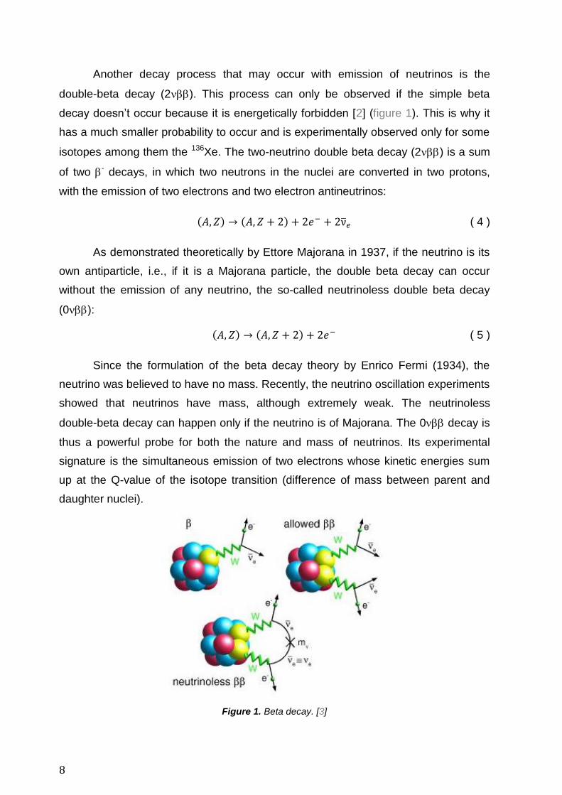
In figure 2 is depicted the expected double beta decay energy spectrum, with
the first large peak corresponding to the 2 decay events and the second peak,
much smaller, to the hypothetical 0 decay events, located at exactly the value
of the decaying isotope (Ke being the sum kinetic energy of the two particles). The
principal advantage of using the 136Xe for this experiment is that these two peaks are
relatively distant from one another, minimizing the overlap possibility [4]. This is due
to the high Q-value (parent-daughter nuclei energy difference [5]) of the 136Xe
transition, where [6]. There are other advantages for using this
isotope, such as its natural high abundance (8.86%) and quite simple enrichment
technique; it offers exceptional intrinsic energy resolution as detection medium; the
ionization tracks that the 0 decay events produce in the gas, allows the
unambiguous identification of the searched events and the rejection of background
in the region of interest of the experiment [2].
Figure 2. Double beta decay energy spectrum. Ke is the sum kinetic energy
of the two particles and Q the Q value of the decaying isotope. [7]
There is no evidence to the date of the observation of the 0 decay process,
however leading experiments in the field have set low limits to its half-life and to the
effective mass of the neutrino. The most recent limits have been set very recently by
the EXO-200 experiment (Nature, 4th of June 2014) with a half-life of the 0 decay
greater than 1.1×1025 years (at the 90% confidence level). This corresponds to an
upper limit of the Majorana neutrino mass of 190450 meV. The search of the 0
decay must hence be pursued with an improved detection technique, including higher
10
energy resolution and better background suppression. The NEXT experiment we
describe in the following section aims at pursuing these goals.
1.2. The NEXT-100 experiment
NEXT-100 is an experiment that will take place at the Laboratorio Subterráneo
de Canfranc (LSC) in Spain [8], and purposes the finding of the neutrinoless double
beta decay (0) of the isotope 136Xe. The experimental evidence of the 0 decay
would have fundamental implications in physics. Indeed, this process is forbidden in
the standard model of particles because it violates the lepton number conservation
and is only possible if the neutrino is a Majorana particle, i.e. identical to its anti-
particle. This phenomenon, if observed, would explain the cosmic asymmetry
between matter and antimatter [9, 10]. It would also provide a direct measure of the
neutrino mass [11, 12]. It will be used 100 kg of the xenon isotope as it offers
scalability to large masses of , that would be necessary if no signal is found, and a
low background rate. The place were the experiment is going to be made was chosen
so that the background of cosmogenic origin can be significantly reduced [13].
1.2.1. Design concepts
NEXT-100 experiment uses a TPC (Time Projection Chamber) filled with 100
kg of high-pressure gaseous xenon with 90% enrichment of the isotope 136Xe and
operated in electroluminescence (EL) mode [4][14]. The gas will be at 10 to 15 bar of
pressure.
As it will operate at high pressure it is an HPGXe TPC, High Pressure Gas
Xenon Time Projection Chamber. It may provide a high-energy resolution close to the
theoretical limit of ∼0.3% at full width at half maximum (FWHM) at the Q-value of
136Xe [15].
There are several fundamental concepts in what NEXT-100 is based, such as
the use of electroluminescence to achieve its high target resolution; two different
11
readout technologies, calorimetric and tracking; low radioactive materials; the
scalability to ton-scale isotope masses [13]. The detector scheme is depicted in figure
3.
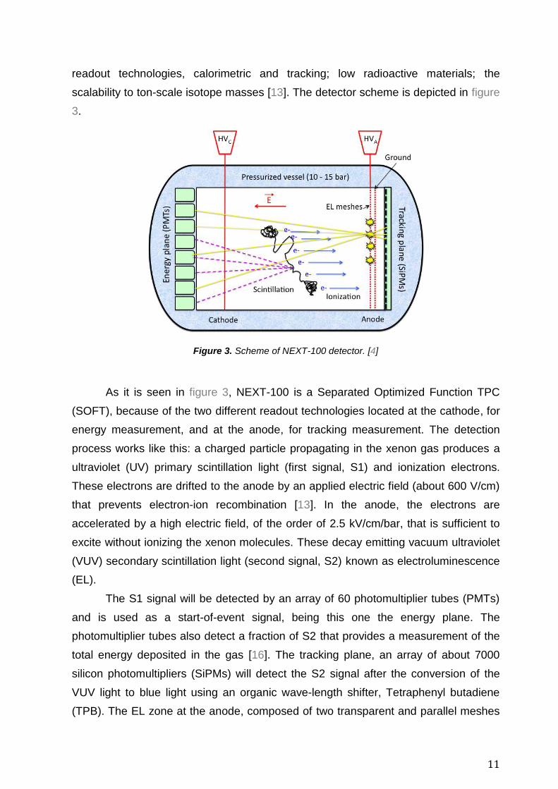
Figure 3. Scheme of NEXT-100 detector. [4]
As it is seen in figure 3, NEXT-100 is a Separated Optimized Function TPC
(SOFT), because of the two different readout technologies located at the cathode, for
energy measurement, and at the anode, for tracking measurement. The detection
process works like this: a charged particle propagating in the xenon gas produces a
ultraviolet (UV) primary scintillation light (first signal, S1) and ionization electrons.
These electrons are drifted to the anode by an applied electric field (about 600 V/cm)
that prevents electron-ion recombination [13]. In the anode, the electrons are
accelerated by a high electric field, of the order of 2.5 kV/cm/bar, that is sufficient to
excite without ionizing the xenon molecules. These decay emitting vacuum ultraviolet
(VUV) secondary scintillation light (second signal, S2) known as electroluminescence
(EL).
The S1 signal will be detected by an array of 60 photomultiplier tubes (PMTs)
and is used as a start-of-event signal, being this one the energy plane. The
photomultiplier tubes also detect a fraction of S2 that provides a measurement of the
total energy deposited in the gas [16]. The tracking plane, an array of about 7000
silicon photomultipliers (SiPMs) will detect the S2 signal after the conversion of the
VUV light to blue light using an organic wave-length shifter, Tetraphenyl butadiene
(TPB). The EL zone at the anode, composed of two transparent and parallel meshes
12
where the ionization electrons are accelerated, can generate ∼103 photons per
electron. This EL amplification process has very low statistical fluctuation that is
fundamental to achieve the high-energy resolution the experiment aims at [17].
SiPMs are responsible to measure the topology of the events, i.e., to make the
3-D image of the two electron tracks of the events. The SiPMs plane give the
transversal dimensions (x-y) of the tracks, and the z dimension (that corresponds to
the drift axis) is given by the time between the signals S1 and S2. The signals are
recorded in time intervals of 1 µs during 300 µs that is the full electron drift time in the
TPC (1 µs corresponds to an electron drift of 1 mm along the longitudinal axis).
Knowing the time and the drift velocity, we can infer the z position of the events. The
SiPMs are located at 1 cm pitch (and not less) because 1 cm is the maximal
transversal diffusion of the electrons in the gas when drifting along 1 m distance (the
drift length in NEXT-100). Arranging the SiPMs at smaller distances does not improve
the tracks image.
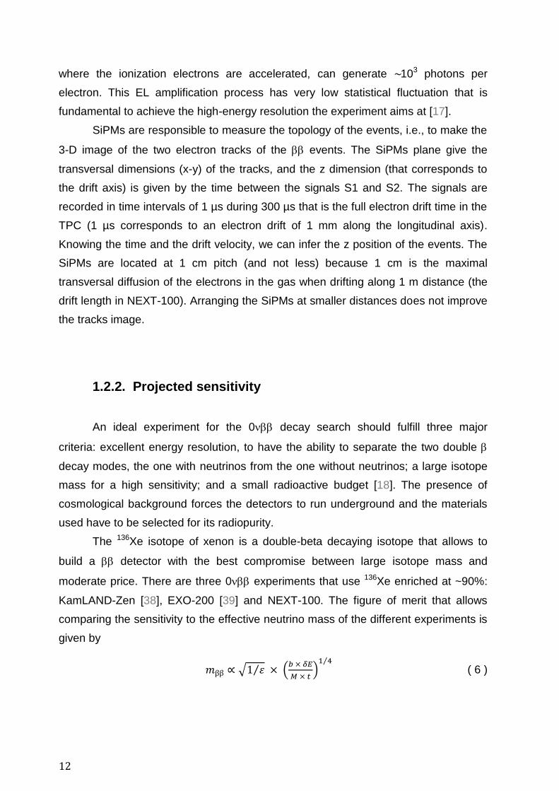
1.2.2. Projected sensitivity
An ideal experiment for the 0 decay search should fulfill three major
criteria: excellent energy resolution, to have the ability to separate the two double
decay modes, the one with neutrinos from the one without neutrinos; a large isotope
mass for a high sensitivity; and a small radioactive budget [18]. The presence of
cosmological background forces the detectors to run underground and the materials
used have to be selected for its radiopurity.
The 136Xe isotope of xenon is a double-beta decaying isotope that allows to
build a detector with the best compromise between large isotope mass and
moderate price. There are three 0 experiments that use 136Xe enriched at ~90%:
KamLAND-Zen [38], EXO-200 [39] and NEXT-100. The figure of merit that allows
comparing the sensitivity to the effective neutrino mass of the different experiments is
given by
√ ⁄ (
) ⁄
( 6 )
13
where is the detector detection efficiency, b the background level (in
counts/keV/kg/year), E the detector energy resolution, M the isotope mass and t the
measurement time (in year). The figure 4 shows the projected sensitivity for the three
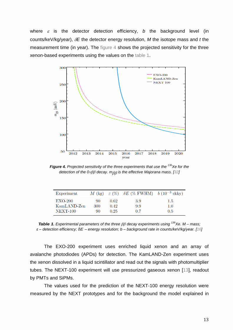
xenon-based experiments using the values on the table 1.
Figure 4. Projected sensitivity of the three experiments that use the 136
Xe for the
detection of the 0 decay. m is the effective Majorana mass. [32]
Table 1. Experimental parameters of the three decay experiments using 136
Xe. M – mass;
ε – detection efficiency; δE – energy resolution; b – background rate in counts/keV/kg/year. [16]
The EXO-200 experiment uses enriched liquid xenon and an array of
avalanche photodiodes (APDs) for detection. The KamLAND-Zen experiment uses
the xenon dissolved in a liquid scintillator and read out the signals with photomultiplier
tubes. The NEXT-100 experiment will use pressurized gaseous xenon [13], readout
by PMTs and SiPMs.
The values used for the prediction of the NEXT-100 energy resolution were
measured by the NEXT prototypes and for the background the model explained in
14
[18]. The prototypes for NEXT-100 are the NEXT-DEMO [19], the demonstrator
prototype described in the following section, and the NEXT-DBDM [20], a small NEXT
prototype built at LBNL (Laurence Berkley National Laboratory) for dark matter and
double-beta search. The experimental results on energy resolution measured with
these two prototypes have indicated that the gaseous xenon TPC using
electroluminescence can achieve an energy resolution near the intrinsic statistical
limit of the xenon gas.
Despite the late start of the NEXT-100, the better energy resolution and
background suppression capability will make it achieve best sensitivity faster than the
other two xenon-based experiments. By 2020 NEXT-100 should be at a sensitivity of
103 meV, for the effective Majorana mass. If the neutrino mass is above the limit of
100 meV, the three experiments have the chance of making a discovery by 2020.
These three experiments are expected to attain a sensitivity of 30-50 meV after a total
exposure of 10 ton a year [18].
1.3. NEXT-DEMO
NEXT-DEMO is a demonstrator and a technological test-bed prototype for the
NEXT-100 detector, which is presently in operation in a semi-clean room at IFIC
(Instituto de Física Corpuscular [40]) laboratory, in Valencia, Spain. It is an HPGXe
TPC (with 1 kg of pure xenon) (figure 5) that was constructed to test and prove the
technological performance expected for NEXT-100. In this prototype the important
issues investigated were the energy resolution, the reconstruction of the topological
signature of electrons in the gas, long drift lengths and electron lifetime, high
voltages, gas recirculation, purification and leaks, and the collection of light [21].
Inside the stainless steel pressure vessel there is circulation of natural xenon,
in a closed loop with a system of purifying filters (getters). This pressure vessel
withstands up to 15 bar. It is cylindrical, 3 mm thick, with 30 cm of diameter and 60
cm of length. Inside the electrical field cage, a light tube made out of PTFE
(Polytetrafluoroethylene, also known as Teflon) is mounted and is used to improve
the light collection. The light tube is coated with the wavelength shifter TPB to
improve the light yield in the TPC. There are three metallic wire grids that make the
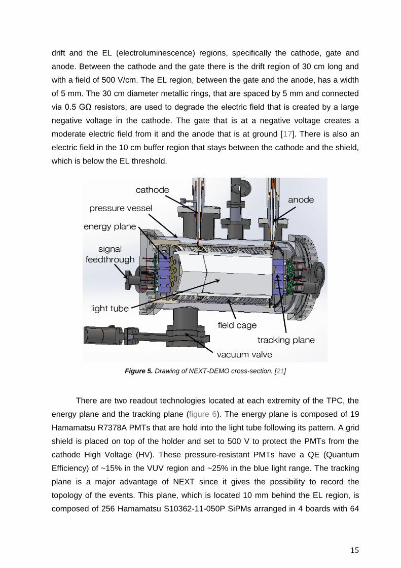
15
drift and the EL (electroluminescence) regions, specifically the cathode, gate and
anode. Between the cathode and the gate there is the drift region of 30 cm long and
with a field of 500 V/cm. The EL region, between the gate and the anode, has a width
of 5 mm. The 30 cm diameter metallic rings, that are spaced by 5 mm and connected
via 0.5 GΩ resistors, are used to degrade the electric field that is created by a large
negative voltage in the cathode. The gate that is at a negative voltage creates a
moderate electric field from it and the anode that is at ground [17]. There is also an
electric field in the 10 cm buffer region that stays between the cathode and the shield,
which is below the EL threshold.
Figure 5. Drawing of NEXT-DEMO cross-section. [21]
There are two readout technologies located at each extremity of the TPC, the
energy plane and the tracking plane (figure 6). The energy plane is composed of 19
Hamamatsu R7378A PMTs that are hold into the light tube following its pattern. A grid
shield is placed on top of the holder and set to 500 V to protect the PMTs from the
cathode High Voltage (HV). These pressure-resistant PMTs have a QE (Quantum
Efficiency) of ~15% in the VUV region and ~25% in the blue light range. The tracking
plane is a major advantage of NEXT since it gives the possibility to record the
topology of the events. This plane, which is located 10 mm behind the EL region, is
composed of 256 Hamamatsu S10362-11-050P SiPMs arranged in 4 boards with 64
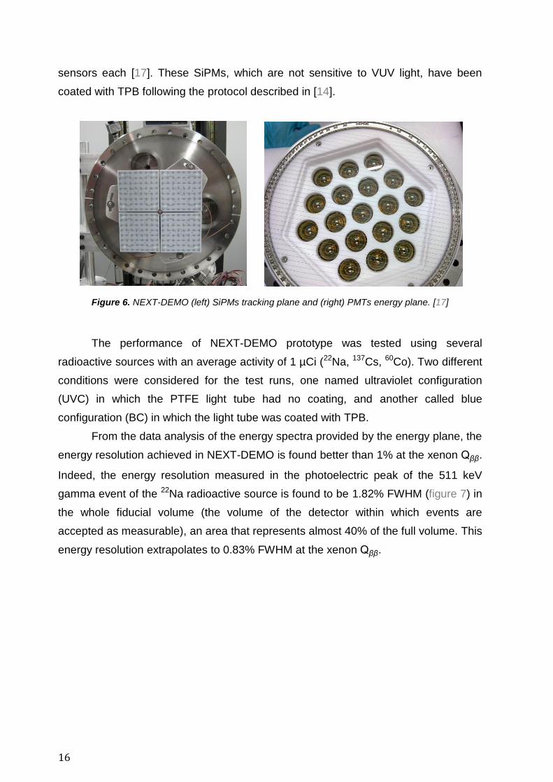
16
sensors each [17]. These SiPMs, which are not sensitive to VUV light, have been
coated with TPB following the protocol described in [14].
Figure 6. NEXT-DEMO (left) SiPMs tracking plane and (right) PMTs energy plane. [17]
The performance of NEXT-DEMO prototype was tested using several
radioactive sources with an average activity of 1 µCi (22Na, 137Cs, 60Co). Two different
conditions were considered for the test runs, one named ultraviolet configuration
(UVC) in which the PTFE light tube had no coating, and another called blue
configuration (BC) in which the light tube was coated with TPB.
From the data analysis of the energy spectra provided by the energy plane, the
energy resolution achieved in NEXT-DEMO is found better than 1% at the xenon .
Indeed, the energy resolution measured in the photoelectric peak of the 511 keV
gamma event of the 22Na radioactive source is found to be 1.82% FWHM (figure 7) in
the whole fiducial volume (the volume of the detector within which events are
accepted as measurable), an area that represents almost 40% of the full volume. This
energy resolution extrapolates to 0.83% FWHM at the xenon .
17
Figure 7. (left) Energy spectrum of γ-ray events from 22
Na source.
(right) Gaussian fit to the 511 keV photoelectric peak. [21]
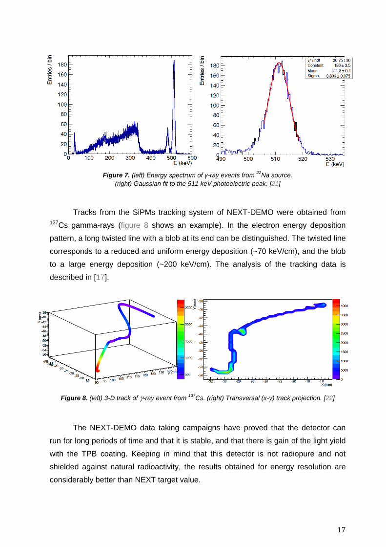
Tracks from the SiPMs tracking system of NEXT-DEMO were obtained from
137Cs gamma-rays (figure 8 shows an example). In the electron energy deposition
pattern, a long twisted line with a blob at its end can be distinguished. The twisted line
corresponds to a reduced and uniform energy deposition (~70 keV/cm), and the blob
to a large energy deposition (~200 keV/cm). The analysis of the tracking data is
described in [17].
Figure 8. (left) 3-D track of -ray event from 137
Cs. (right) Transversal (x-y) track projection. [22]
The NEXT-DEMO data taking campaigns have proved that the detector can
run for long periods of time and that it is stable, and that there is gain of the light yield
with the TPB coating. Keeping in mind that this detector is not radiopure and not
shielded against natural radioactivity, the results obtained for energy resolution are
considerably better than NEXT target value.
18
1.4. NEXT-WHITE (NEW)
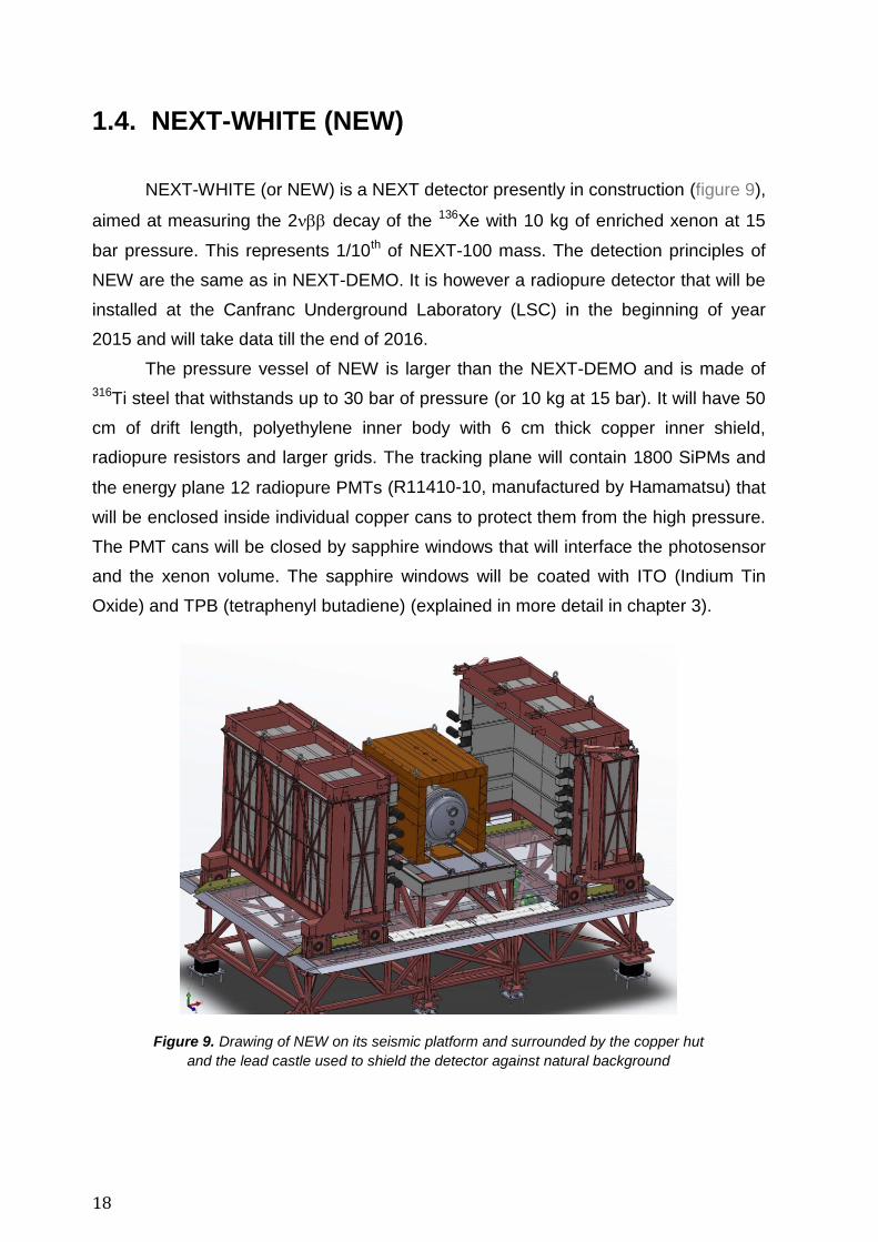
NEXT-WHITE (or NEW) is a NEXT detector presently in construction (figure 9),
aimed at measuring the 2 decay of the 136Xe with 10 kg of enriched xenon at 15
bar pressure. This represents 1/10th of NEXT-100 mass. The detection principles of
NEW are the same as in NEXT-DEMO. It is however a radiopure detector that will be
installed at the Canfranc Underground Laboratory (LSC) in the beginning of year
2015 and will take data till the end of 2016.
The pressure vessel of NEW is larger than the NEXT-DEMO and is made of
316Ti steel that withstands up to 30 bar of pressure (or 10 kg at 15 bar). It will have 50
cm of drift length, polyethylene inner body with 6 cm thick copper inner shield,
radiopure resistors and larger grids. The tracking plane will contain 1800 SiPMs and
the energy plane 12 radiopure PMTs (R11410-10, manufactured by Hamamatsu) that
will be enclosed inside individual copper cans to protect them from the high pressure.
The PMT cans will be closed by sapphire windows that will interface the photosensor
and the xenon volume. The sapphire windows will be coated with ITO (Indium Tin
Oxide) and TPB (tetraphenyl butadiene) (explained in more detail in chapter 3).
Figure 9. Drawing of NEW on its seismic platform and surrounded by the copper hut
and the lead castle used to shield the detector against natural background
19
NEW has several goals: measure the expected backgrounds from different
isotopes, especially 214Bi and 208Tl, which are the main contaminants in the region of
interest of the NEXT experiment; validate NEXT background model using these
measurements; identify any unexpected source of background; measure 2 decay;
achieve good energy resolution (the goal of NEXT-100 is to reach 0.5% FWHM);
show the topological signature from the 2 and the Tl-208 double escape peak;
and certify the technology and the underground operation with enriched xenon [23].
NEW will be operated in two phases. The first one, at IFIC to run some tests
and cleaning. Later, it will be moved to the LSC (at Canfranc) for physic
measurements.
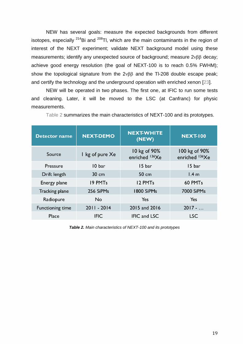
Table 2 summarizes the main characteristics of NEXT-100 and its prototypes.
Table 2. Main characteristics of NEXT-100 and its prototypes
20
1.5. This Master Thesis
This Master Thesis aims at contributing to NEW detector development through
EL light conversion and transmission studies.
The first topic of the thesis addressing the light conversion in NEXT TPC
(chapter 2) comprises an experimental study of the SiPMs photodetection efficiency
(PDE) and the TPB quantum efficiency (QE). For the PDE study three different SiPMs
were considered. For the TPB QE measurements, different types of TPB coatings
were tested in several conditions.
The second topic of the thesis addressing the light transmission (chapter 3)
comprises studies of the optical transmission and conductivity of different conductive
coatings produced in the laboratory and used in NEW for the electrical screening of
the photosensors readout planes. It comprises also a study of the light transmission
from the xenon active volume to the PMTs with different coupling options to the
sapphire window of the copper cans.
In chapter 4 we summarize and conclude the studies performed in this thesis,
and in chapter 5 possible applications to medical physics are outlined.
21
Chapter 2
Light conversion studies
The tracking plane in NEXT, which is composed of small silicon
photomultipliers (SiPMs), is used to reconstruct the events topology for the
identification of the events and the distinction of background events which have a
different topological signature. In this chapter the photon-detection efficiency of three
different SiPMs is described and comparison between the SiPMs is discussed. We
describe also the conversion efficiency of different TPB coatings produced by vacuum
evaporation and in plastic mixtures applied by spin-coating.
The measurements of the SiPMs photo-detection efficiency was intended in
the VUV range, especially at the xenon scintillation wavelength (~172 nm) using a
vacuum monochromator. However, in the monochromator we used (Model VM-502
from Princeton Instruments Corporation) borrowed from Coimbra University, a
vacuum leak appeared we could not solve in the span of this thesis schedule. We
thus performed the measurements in the UV range using a LED (Light Emitting
Diode) emitting at 285 nm ± 5 nm, operated in continuous mode at room temperature
(~25 ºC). The experimental procedure we will use for the VUV measurements of the
PDE, as soon as the vacuum monochromator is repaired and available, is the same
as that used with the LED.
The two measurements described in this chapter are important for the
simulation of the SiPMs response in NEXT and for the comparison to the
experimental data.
22
2.1. Measurements of SiPMs Photo-detection Efficiency
The Silicon Photomultipliers (SiPM) or MPPC (multi-pixel photon counters,
which are SiPM prototypes from Hamamatsu) are small solid state photosensors with
detection levels comparable to Photomultipliers (PMT), which allow a high
segmentation of the tracking plane at a moderate price (12 Euros per unit). The ones
used in NEXT (Hamamatsu S10362-11-050P) have an active area of 1 mm2, a
nominal gain of 7.5×10⁵, and a reduced radioactivity budget, expected to be of the
order of a few µBq/kg for the 238U and 232Th radioactive chains [24].
The noble gas xenon scintillates in the VUV (peak at 172 nm), domain at which
the SiPMs are not sensitive. A wavelength shifter is thus needed. Using the organic
compound Tetraphenyl Butadiene (TPB), scintillation grade (> 99%) from Sigma-
Aldrich, it is possible to shift the scintillation light from the VUV to the visible, as
follows: the short wavelength photons (< 340 nm) are absorbed by the TPB molecules
and re-emitted in the blue wavelength range, with a maximum yield at 430 nm
[13][25].
Two of the SiPMs tested here (Hamamatsu S10362-11-50P and S10362-33-
50P) were coated with evaporated TPB (see next subsection) directly on their plastic
window with an areal density of 0.1 mg/cm2, i.e., a thickness of 130 ± 10 nm. The
third SiPM (Hamamatsu S10362-11-50P) was not coated. The SiPMs S10362-11-50P
have 400 pixels and an active area of 1×1 mm2. The SiPM S10362-33-50P has 3600
pixels and an active area of 3×3 mm2.
2.1.1. Measurement principle
The PDE (Photon Detection Efficiency) is the percentage of incident photons
recorded by the SiPMs. The PDE of the SiPM is affected by the epoxy resin material
of the window that protects its silicon active area, and which has poor transparency to
photons below 300 nm. The QE (Quantum Efficiency) of the SiPMs in the visible light
is almost 100%. However, the PDE is smaller due to several factors like the reduced
coverage of the active area because of the microcells structure (fill factor of 30-60%),
and the probability that electrons and holes initiate an avalanche or electrical
breakdown in the depleted region (Pav) [13]. The PDE is defined by
23
( 7 )
Experimentally the PDE is determined by comparing the number of recorded
photons (Nrec) with the number of simultaneously incident photons (Ninc), expressed in
equation 8.
[ (
)] ( 8 )
Npixels being the total number of pixels or microcells in the SiPM.
For low illumination levels the SiPM response is linear, since the number of
incident photons is small compared to the number of pixels, and the equation
presented before can be approximated to
( 9 )
In order to measure the PDE of the three SiPM prototypes we used the
photocurrent method (also used by Hamamatsu) that consists in determining the
recorded and the incident number of photons from the photosensors photocurrent
after subtraction of the dark current.
The number of recorded photons per unit of time in the SiPMs is given by its
output current (ISiPM) after the subtraction of the dark current, divided by the gain
provided by the manufacturer for a specific voltage at room temperature, multiplied by
the elementary charge (qe):
( 10 )
On the other hand, the number of incident photons was determined using a
calibrated photosensor, the PMT R8530 ref. 2773 from Hamamatsu, which was
operated without gain. That is to say, with the output current (IPMT) taken from the first
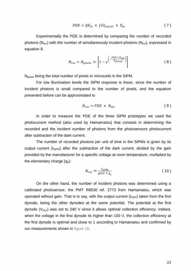
dynode, being the other dynodes at the same potential. The potential at the first
dynode (VDy1) was set to 240 V since it allows optimal collection efficiency. Indeed,
when the voltage in the first dynode its higher than 100 V, the collection efficiency at
the first dynode is optimal and close to 1 according to Hamamatsu and confirmed by
our measurements shown in figure 10.
24
Figure 10. PMT photocurrent as a function of the bias voltage of the first dynode
The number Ninc of recorded photons in the SiPM is thus determined by
( 11 )
where QEPMT is the PMT quantum efficiency (0.3199 at 285 nm), CE its collection
efficiency (~100% when the voltage between the photocathode and the first dynode is
above 100 V) and Fgeom the geometrical factor that accounts for the difference
between the active areas of the PMT and of the SiPM.
The PDE measurement with the photocurrent method is not very precise
because the optical crosstalk and after-pulses in the SiPM photocurrent should be
subtracted to determine the photocurrent truly induced by incident photons. Crosstalk
occurs when secondary photons, which are generated in the avalanche multiplication
process of a SiPM pixel, are detected by other pixels. When the SiPM photon
detection output has a time delay from the light input larger than the recovery time of
the pixels it is called afterpulse. This is because, during the avalanche multiplication
process, electrons from the avalanche may be trapped and released later, inducing a
new avalanche a few hundreds of ns after the primary one [34].
However, since the objective of this PDE measurement is to compare SiPMs
with and without TPB coating, the photocurrent method is sufficient enough. Also, for
the simulation of the NEXT tracking plane, the absolute PDE is not needed for
25
comparison with the experimental data as these include crosstalk and afterpulses
counts, which are not discriminated and subtracted.
2.1.2. Experimental Setup
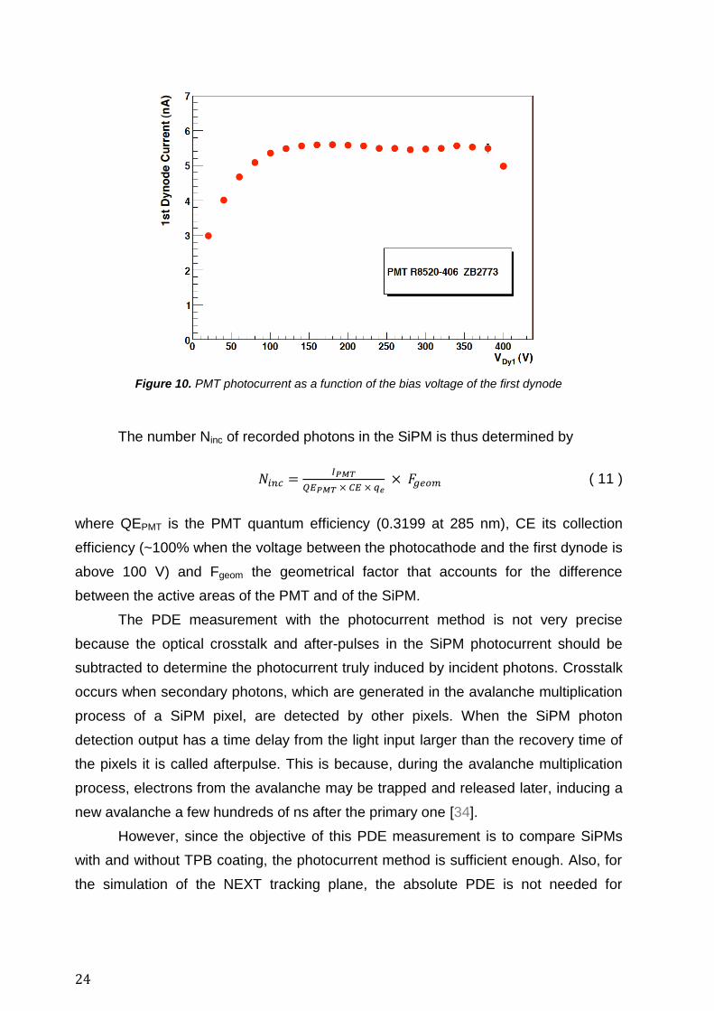
To measure the PDE we mounted a setup with a vacuum monochromator
used as a light source coupled to a cylindrical stainless steel vacuum chamber of 800
mm and 320 mm inner diameter (figure 11), a primary pump, a turbomolecular pump,
photosensors, and apparatus for current measurements and voltage supply. In order
to reach the desired VUV wavelengths bellow 200 nm, we used the vacuum
monochromator model Acton VM 502 from Princeton Instruments. This
monochromator has 1200 G/mm gratings, a focal length of 0.2 m, a wavelength range
from ~30 nm to 546.1 nm, and two slits adjustable from 5 µm to 3 mm.
Figure 11. The vacuum monochromator used, coupled to the cylindrical vacuum chamber
26
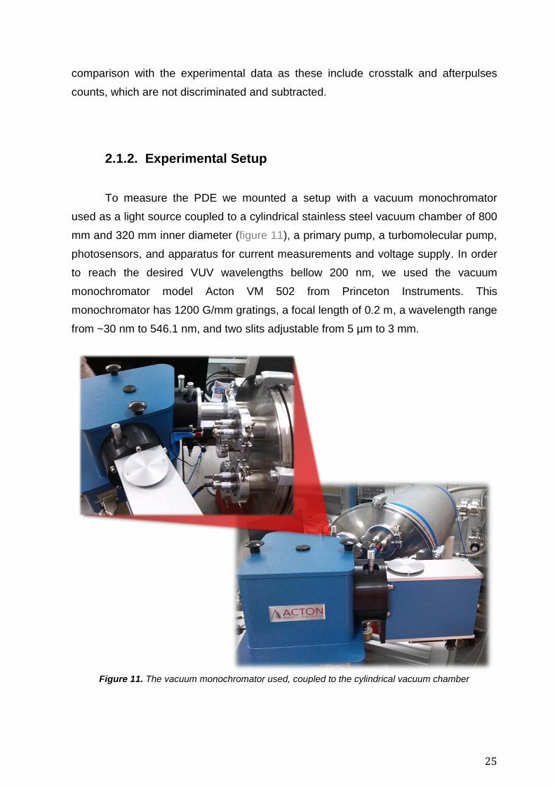
Several tests were made to characterize the monochromator. The PMT was
placed inside the vacuum chamber, as close as possible to the light source in the port
connected to the monochromator, as shown in figure 11. The PMT was connected to
an electrometer (Keithley 6517B), used to measure its photocurrent. In figure 12 the
PMT photocurrent measured is shown as a function of wavelength between 160 nm
and 550 nm and at different slit openings of the monochromator. The PMT dark
current for the measurements made with the slits opened 1 mm was 1.04 nA, for the
2 mm aperture it was 1.07 nA, and with an aperture of 3 mm it was 1.03 nA. The
result from this test shows that the PMTs photocurrent follows the lamp emission
pattern in the UV and visible ranges and that the more open the slits are the more
photoelectrons are collected by the PMT. However, the light below 175 nm is not
detected by the PMT.
Figure 12. PMT photocurrent as a function of wavelength.
The PMT is illuminated with the monochromator light and different slit apertures
This should not happen since the PMT is as sensitive in the VUV as it is in the
visible, as can be seen in the figure 13.
27
Figure 13. PMT R8520-06 quantum efficiency as a function of wavelength
The monochromator was working properly but a vacuum leak prevents us from
doing the planned VUV measurements. Because of that, we had to make the
measurements in the UV as described next.
Figure 14 shows the experimental setup used for the PDE measurements in
air, using a UV light emitting diode. The same stainless steel cylindrical vacuum
chamber was used. Inside the chamber the following elements were placed: a LED
(with emission peak at 285 nm ± 5 nm), a PTFE (or Teflon) reflector plane used to
diffuse and reflect the light, and in front of it a plane supporting the PMT and the
SiPMs. The calibrated PMT was used as a reference photosensor. The LED
illuminates the polished PTFE plane located at a large distance that ensures the
uniformity of the reflected light received by the photosensors. A sourcemeter (model
Keithley 224) provided to the LED a stable current from 0.7 mA to 30.0 mA, in order
to obtain proportionally different photon intensities. 34 supply current values were
used. The PMT was connected to the Keithley 6517B electrometer, used to measure
its photocurrent, and to a High Voltage (HV) supply. The SiPMs were connected to a
picoammeter (Keithley 6487), which measured their electrical current, and also to the
electrometer that provided their voltage bias (close to 70 V). The bias used for the
SiPMs S10362-11-50p was of 73.45 V and for the SiPM S10362-33-50p it was of
71.43 V.
The average dark currents measured for the SiPMs S10362-11-50P were:
18.45 nA ± 0.39 nA for the non-coated SiPM and 17.96 nA ± 0.19 nA for the coated
one. The average dark current of the SiPMs S10362-33-50P coated was 1.83 µA ±
2.31 nA. As for the PMT, its average dark current was 1.34 nA ± 3.69 pA. All of the
28
current values measured, including the dark currents, are given as the mean of 100
samples measured automatically by the picoammeter, with the corresponding
standard deviation taken as a statistical error.
Figure 14. Experimental setup used for the PDE measurements
2.1.3. Results and Conclusions
In figure 15 the response curve of the SiPMs used is depicted, two TPB coated
and one non-coated, with increasing incident photons intensities. The non-coated
(NC) 1×1 mm2 sample and the coated (C) 1×1 mm2 and 3×3 mm2 samples have the
same pixel size. The PDEs obtained, determined from a linear fit at low illumination
levels, were 1.60 ± 0.01% for the 1×1 NC, 13.87 ± 0.04% for the 1×1C and 16.06 ±
0.12% for the 3×3C. The PDE value of the SiPM 3×3C is slightly higher than the PDE
of the 1×1C at the wavelength of the converted photons, as specified by Hamamatsu.
The increase of PDE from one sample coated with TPB to other non-coated is about
a factor 9 in these measurement conditions. Changing the LED operation from
continuous to pulsed mode with duration of 1 µs, as it is usually operated in NEXT for
calibration purposes, doesn’t change significantly these results.
The theoretical response curves drawn in the figure 15 with dashed dots
correspond to equation 8. From this theoretical curve, we can observe that the
response of the SiPM 1×1C deviates from linearity when approximately a quarter of
the total number of pixels is simultaneously excited to produce a photoelectron (~100)
[13]. It can be noted that at higher illumination levels the recorded number of photons
29
is lower than the expected, which indicates saturation in the SiPM due to the dead
time of the individual pixels of the order of 20-50 ns, and to the increasing probability
for simultaneous photons falling in the same pixel. In the theoretical curve, the SiPM
microcells are considered to respond independently to incident photons, which is not
accurate. The microcells are not independent, so once a microcell is fired by an
incident photon, a number of other cells are fired too because of the crosstalk
photons that are created and afterpulses. This phenomenon implies that the
occupancy of the cells per one photon induces the occupancy of other cells.
Consequently, these cells will not be able to detect incident photons until they
recover. So at increasing incident photon intensity, the number of photons recorded
will be lower than predicted by equation 8.
Figure 15. Response curve of the SiPMs S1036211-50P (1×1 mm
2) (up)
and S10362-33-50P (3×3 mm2) (down)
30
The PDE measurements performed here indicate a large gain in the sensitivity
of the SiPMs in the UV range due to TPB. A large factor, close to 9, has been
measured comparing to the non-coated SiPM. This value however depends on the
thickness and quality of the TPB layer that could be altered by environmental agents
as oxygen and humidity. These factors are not evaluated here.
For the TPB coated SiPM samples the magnitude we have measured is an
effective PDE of the photosensor at 285 nm, about 14% (1×1C) and 16% (3×3C).
This can be expressed as follows:
( ( ( ( 12 )
where QE is the TPB conversion efficiency or quantum efficiency, PDE(430 nm) is the
PDE of the SiPM considered at the emission peak of the TPB i.e. 430 nm provided by
Hamamatsu (~50% for 1×1 and 3×3), and Geomfactor is about 50% as only about half
of the isotropically emitted photons from the TPB layer falls onto the SiPM window.
Therefore, we can infer from our effective PDE measurement an estimation of the
TPB fluorescence or quantum efficiency.
(
( ( ( 13 )
This estimation of the TPB QE at 285 nm is compatible with the TPB
fluorescence efficiency measured at the same wavelength and for the same coating
thickness described in the following section.
2.2. Measurement of TPB Quantum Efficiency
The TPB (tetraphenyl butadiene) is an organic chemical compound that is
used as a wavelength shifter in neutrino and dark matter experiments. In the NEXT-
100 experiment the silicon photomultipliers (SiPMs) are used to detect VUV (Vacuum
Ultraviolet) scintillation emitted by the noble gas xenon. Since silicon photomultipliers
are insensitive to VUV light (the emission spectrum of the xenon scintillation has its
peak at 172 nm) and because they are most sensitive at ~440 nm, it is necessary to
shift the VUV light to a longer wavelength.
31
The Conversion efficiency depends on the layer thickness and the way the
coating is produced, evaporated or mixed with a polymer. We present here the
measurements of the conversion efficiency of TPB coatings deposited on quartz
substrates and applied using two alternative procedures: vacuum evaporation and
spin-coating of TPB and polystyrene (PS) mixtures. The coatings are compared for
different percentages of each material in the mixture, and different spin-coating
velocities and spin-coating duration. This implies that the thickness of each sample is
different. Some measurements of the fluorescence efficiency were made for different
wavelengths between 250 and 400 nm.
The reason to consider these mixtures is because they are simpler to obtain
than evaporated TPB, and are possibly less prone to degradation due to
environmental agents.
2.2.1. Evaporated TPB coatings
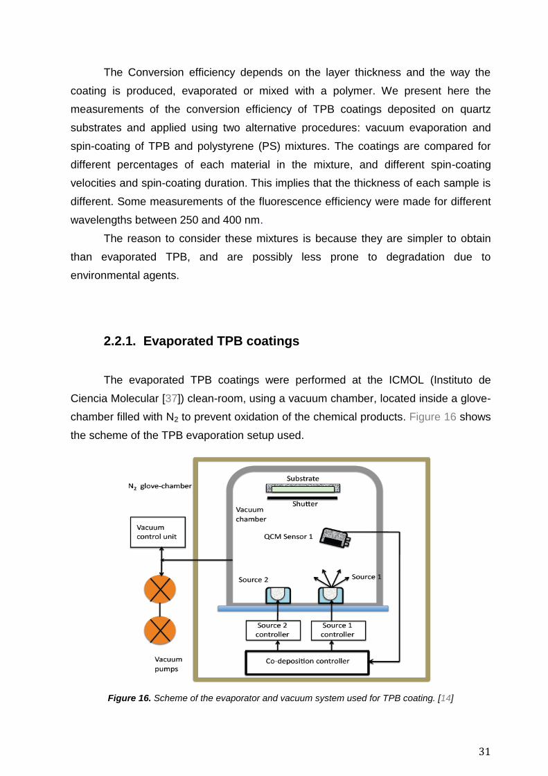
The evaporated TPB coatings were performed at the ICMOL (Instituto de
Ciencia Molecular [37]) clean-room, using a vacuum chamber, located inside a glove-
chamber filled with N2 to prevent oxidation of the chemical products. Figure 16 shows
the scheme of the TPB evaporation setup used.
Figure 16. Scheme of the evaporator and vacuum system used for TPB coating. [14]
32
The vacuum inside the evaporator is made by a diaphragm pump and a turbo-
molecular pump. The vacuum level attained was close to 10-7 mbar. The substrate is
placed on a sample-holder that is fixed on a spinning disk 15 cm above the crucible.
Once the vacuum-chamber is closed, the pumps start to evacuate the N2 till the point
where the optimum vacuum level is reached (4×10⁻⁷ mbar). A shutter located beneath
the sample-holder is used to protect the substrate when necessary. With the shutter
closed, heating of the crucible filled with TPB is started. A cartridge provides the heat
where the electrical current can be adjusted so that it allows the control of the
evaporation rate. At high vacuum, the TPB starts to evaporate at 75 ºC (at
atmospheric pressure that value is of 203 ºC). Although it is possible to evaporate
simultaneously four different compounds in the evaporator chamber, only one source
(or crucible) was used at a time.
The thickness of the TPB deposited on the substrate is measured with an ultra
high precision Quartz Crystal Microbalance (QCM) detector from Sigma Instruments,
located between the crucible and the substrate [14]. This deposition sensor is capable
of measuring in real time mass changes ranging from micrograms to fractions of
nanogram. Thickness and deposition rates are measured in kiloAngström (kA) and
kA/s respectively. Prior to the shutter opening, the deposition rate has to be stable
(between 1.8 and 2.4 Å/s) in order to ensure a steady deposition of the evaporated
TPB on the substrate. The shutter is then opened and the spinning of the sample-
holder is activated. This spinning is crucial to ensure the uniformity of the TPB
deposition. In order to restrain the deposition rate and thickness (areal mass), the
temperature in the crucible, and the vacuum level, these values are displayed in the
deposition control units.
The shutter is closed when the desired thickness level is reached. After the
coating process, the samples are stored in dark and in N2 atmosphere to prevent
degradation of TPB due to oxidation and hydration.
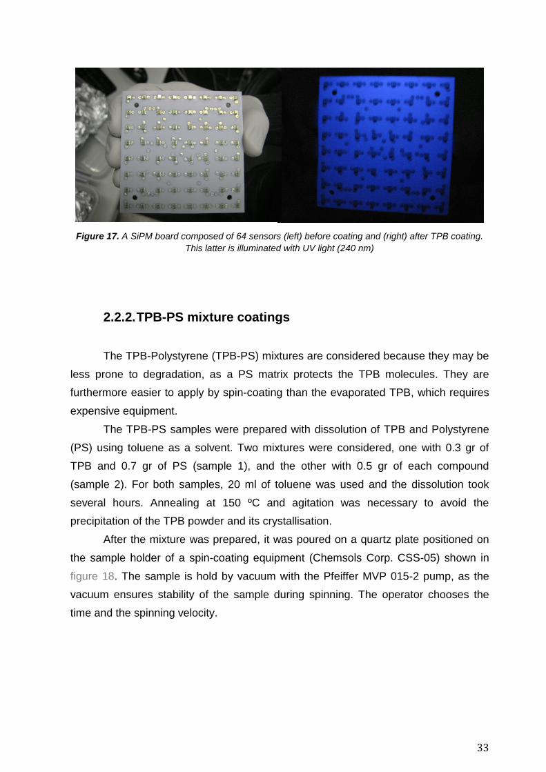
Figure 17 shows a SiPM board before the TPB coating and the same board
with the coating, being this last sample illuminated with a UV light at 240 nm. As it is
seen in the picture, the converted light is blue.
33
Figure 17. A SiPM board composed of 64 sensors (left) before coating and (right) after TPB coating.
This latter is illuminated with UV light (240 nm)
2.2.2. TPB-PS mixture coatings
The TPB-Polystyrene (TPB-PS) mixtures are considered because they may be
less prone to degradation, as a PS matrix protects the TPB molecules. They are
furthermore easier to apply by spin-coating than the evaporated TPB, which requires
expensive equipment.
The TPB-PS samples were prepared with dissolution of TPB and Polystyrene
(PS) using toluene as a solvent. Two mixtures were considered, one with 0.3 gr of
TPB and 0.7 gr of PS (sample 1), and the other with 0.5 gr of each compound
(sample 2). For both samples, 20 ml of toluene was used and the dissolution took
several hours. Annealing at 150 ºC and agitation was necessary to avoid the
precipitation of the TPB powder and its crystallisation.
After the mixture was prepared, it was poured on a quartz plate positioned on
the sample holder of a spin-coating equipment (Chemsols Corp. CSS-05) shown in
figure 18. The sample is hold by vacuum with the Pfeiffer MVP 015-2 pump, as the
vacuum ensures stability of the sample during spinning. The operator chooses the
time and the spinning velocity.
34
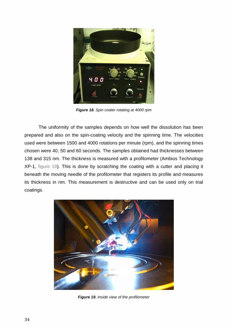
Figure 18. Spin coater rotating at 4000 rpm
The uniformity of the samples depends on how well the dissolution has been
prepared and also on the spin-coating velocity and the spinning time. The velocities
used were between 1500 and 4000 rotations per minute (rpm), and the spinning times
chosen were 40, 50 and 60 seconds. The samples obtained had thicknesses between
138 and 315 nm. The thickness is measured with a profilometer (Ambios Technology
XP-1, figure 19). This is done by scratching the coating with a cutter and placing it
beneath the moving needle of the profilometer that registers its profile and measures
its thickness in nm. This measurement is destructive and can be used only on trial
coatings.
Figure 19. Inside view of the profilometer
35
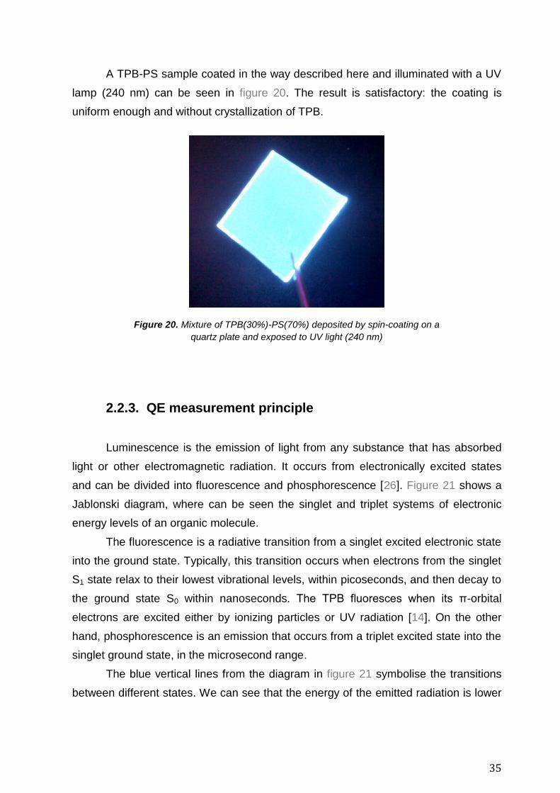
A TPB-PS sample coated in the way described here and illuminated with a UV
lamp (240 nm) can be seen in figure 20. The result is satisfactory: the coating is
uniform enough and without crystallization of TPB.
Figure 20. Mixture of TPB(30%)-PS(70%) deposited by spin-coating on a
quartz plate and exposed to UV light (240 nm)
2.2.3. QE measurement principle
Luminescence is the emission of light from any substance that has absorbed
light or other electromagnetic radiation. It occurs from electronically excited states
and can be divided into fluorescence and phosphorescence [26]. Figure 21 shows a
Jablonski diagram, where can be seen the singlet and triplet systems of electronic
energy levels of an organic molecule.
The fluorescence is a radiative transition from a singlet excited electronic state
into the ground state. Typically, this transition occurs when electrons from the singlet
S1 state relax to their lowest vibrational levels, within picoseconds, and then decay to
the ground state S0 within nanoseconds. The TPB fluoresces when its π-orbital
electrons are excited either by ionizing particles or UV radiation [14]. On the other
hand, phosphorescence is an emission that occurs from a triplet excited state into the
singlet ground state, in the microsecond range.
The blue vertical lines from the diagram in figure 21 symbolise the transitions
between different states. We can see that the energy of the emitted radiation is lower
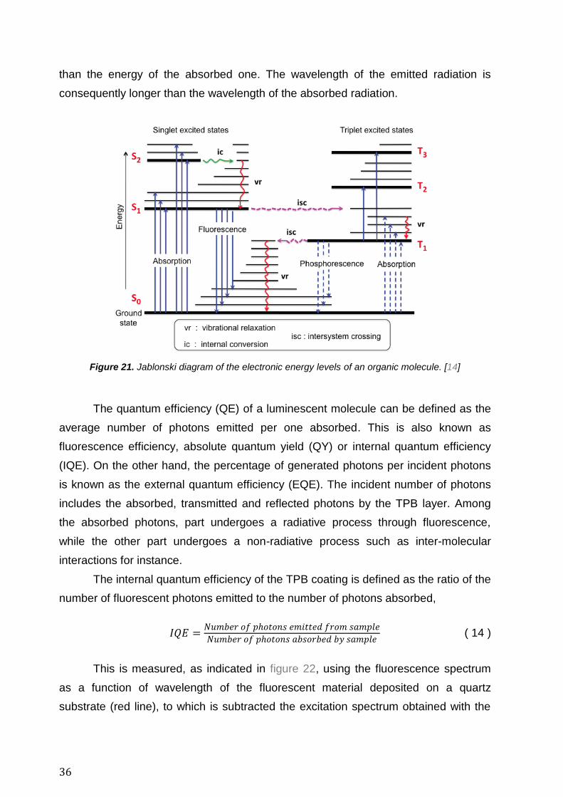
36
than the energy of the absorbed one. The wavelength of the emitted radiation is
consequently longer than the wavelength of the absorbed radiation.
Figure 21. Jablonski diagram of the electronic energy levels of an organic molecule. [14]
The quantum efficiency (QE) of a luminescent molecule can be defined as the
average number of photons emitted per one absorbed. This is also known as
fluorescence efficiency, absolute quantum yield (QY) or internal quantum efficiency
(IQE). On the other hand, the percentage of generated photons per incident photons
is known as the external quantum efficiency (EQE). The incident number of photons
includes the absorbed, transmitted and reflected photons by the TPB layer. Among
the absorbed photons, part undergoes a radiative process through fluorescence,
while the other part undergoes a non-radiative process such as inter-molecular
interactions for instance.
The internal quantum efficiency of the TPB coating is defined as the ratio of the
number of fluorescent photons emitted to the number of photons absorbed,
( 14 )
This is measured, as indicated in figure 22, using the fluorescence spectrum
as a function of wavelength of the fluorescent material deposited on a quartz
substrate (red line), to which is subtracted the excitation spectrum obtained with the
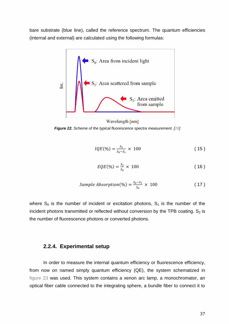
37
bare substrate (blue line), called the reference spectrum. The quantum efficiencies
(internal and external) are calculated using the following formulas:
Figure 22. Scheme of the typical fluorescence spectra measurement. [28]
(
( 15 )
(
( 16 )
(
( 17 )
where S0 is the number of incident or excitation photons, S1 is the number of the
incident photons transmitted or reflected without conversion by the TPB coating. S2 is
the number of fluorescence photons or converted photons.
2.2.4. Experimental setup
In order to measure the internal quantum efficiency or fluorescence efficiency,
from now on named simply quantum efficiency (QE), the system schematized in
figure 23 was used. This system contains a xenon arc lamp, a monochromator, an
optical fiber cable connected to the integrating sphere, a bundle fiber to connect it to
38
the PMA-12 (photonic multichannel analyser, Hamamatsu C10027-01) and a
personal computer.
Figure 23. Czerny-Turner polychromator principle (left) and overall system for QE measurement (right)
The xenon arc lamp provides continuous light output from 250 to 700 nm as a
result of recombination of electrons with ionized Xe atoms [26]. This lamp is rated of
150 W and has an output stability of 1.0% (peak to peak).
The excitation wavelength is selected from the output of the xenon lamp by a
monochromator. This later is used to disperse the white light into various
wavelengths, since it has one exit slit and only one wavelength can pass through that
slit at a time. The excitation light is introduced into the integrating sphere by an optical
fiber.
The function of the integrating sphere is to spatially integrate radiant flux (light).
The concept can be described by the following: the radiation exchange between two
areas on the integrating surfaces is independent of the viewing angle and the
distance between the surface areas. Therefore, the fraction of flux received by any
point on the sphere wall is the same for any other radiation point on the sphere wall
[29]. The diameter of the integrating sphere is of 84 mm. A spectralon (Labsphere)
was mounted on the internal surface of the integrating sphere [30]. This makes the
sphere to have a reflectance of 99%, for wavelengths between 350 nm and 1650 nm,
39
and 96% for wavelengths from 250 nm to 350 nm. The baffle inside the integrating
sphere prevents the light from illuminating directly the photodetector located at the
output port of the sphere. Several optical fibers are bundled to connect the integrating
sphere to the spectrometer PMA-12. This is a compact spectral measurement
apparatus that combines a polychromator and an optical detector into one unit [31].
The polychromator function is to disperse light into different directions through
its several slits, so that the distinct parts of the light spectrum can be separated. To
measure the light at each wavelength, the PMA-12 has a back-thinned photodetector
after each slit of the polychromator. The back-thinned photodetector (BT-CCD
(Charge-coupled device)), a device from Hamamatsu, provides a spectrum range
between 200 nm and 950 nm, has 1024 photosensitive channels and a pixel size
from 24 µm to 2.928 mm. The figure 23 shows the Czerny-Turner polychromator
principle. The grating disperses the incident light and the BT-CCD detects the
dispersed light in the PMA-12.
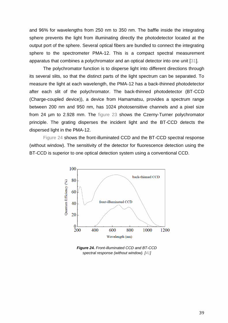
Figure 24 shows the front-illuminated CCD and the BT-CCD spectral response
(without window). The sensitivity of the detector for fluorescence detection using the
BT-CCD is superior to one optical detection system using a conventional CCD.
Figure 24. Front-illuminated CCD and BT-CCD
spectral response (without window). [41]
40
2.2.5. Results and Conclusions
After the selection of the excitation wavelength, we measured the QE as
follows: a reference quartz slice without coating is inserted into the integrating sphere.
The reference spectrum is measured during a certain time (few ms), which can be
chosen by the operator or taken as the default value by the spectrometer software.
The reference spectrum is represented in black in the following plots. When this
measurement is completed, we remove the reference sample and insert the quartz
sample coated with TPB. The fluorescence spectrum is then measured, using the
same input light and duration as the reference. This process is repeated for the
remaining coated samples (the results are the coloured lines in the plots shown here).
The substrate for all the coated samples was made of quartz with the same size and
thickness as the reference.
The quantum efficiency is obtained by measuring the area of the excitation and
fluorescence peaks within selected wavelength ranges. The number of absorbed
photons is calculated as the difference of the areas of the excitation and scattered
peaks within the wavelength range below the fluorescence range. The wavelength
range selected for the fluorescence peak was from ~395 nm to ~680 nm. The value of
the QE is calculated using formula 15, where the reference spectrum is subtracted
from the fluorescence spectrum.
The following figures show the measurements made with evaporated TPB and
with different proportions of TPB-PS mixtures and different thicknesses. For the
evaporated TPB, the coating thicknesses were of 135 nm ± 10 nm (or 0.1 gr/cm2),
150 nm ± 10 nm and two samples of 260 nm ± 10 nm. 16 excitation wavelengths
were used for the QE measurement, between 250 nm ± 3 nm and 400 nm ± 3 nm.
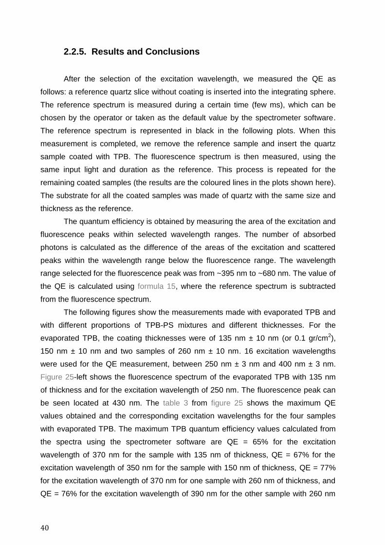
Figure 25-left shows the fluorescence spectrum of the evaporated TPB with 135 nm
of thickness and for the excitation wavelength of 250 nm. The fluorescence peak can
be seen located at 430 nm. The table 3 from figure 25 shows the maximum QE
values obtained and the corresponding excitation wavelengths for the four samples
with evaporated TPB. The maximum TPB quantum efficiency values calculated from
the spectra using the spectrometer software are QE = 65% for the excitation
wavelength of 370 nm for the sample with 135 nm of thickness, QE = 67% for the
excitation wavelength of 350 nm for the sample with 150 nm of thickness, QE = 77%
for the excitation wavelength of 370 nm for one sample with 260 nm of thickness, and
QE = 76% for the excitation wavelength of 390 nm for the other sample with 260 nm
41
of thickness. It is important to stress here that these results given by the spectrometer
software are provided without the statistical and systematic errors. We will further
evaluate these errors by an independent analysis using the data files stored and the
CERN (European Organization for Nuclear Research) data analysis software ROOT.
The values reported in this study have to be considered as preliminary results.
Figure 25. (left) Fluorescence spectra of a sample with evaporated TPB with 135 nm of thickness
(0.1gr/cm2) and for an excitation wavelength of 250 nm. (right) Table 3 – maximum QE values and
corresponding excitation wavelengths measured for the four TPB samples considered
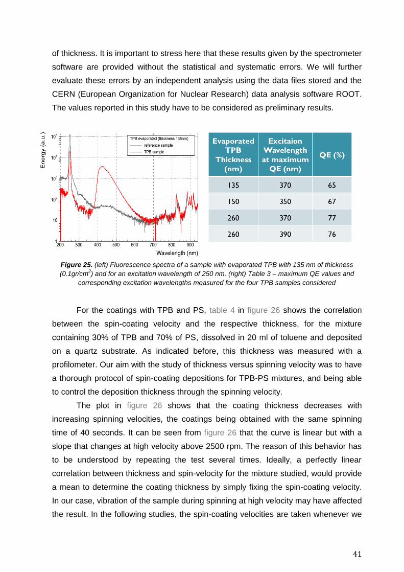
For the coatings with TPB and PS, table 4 in figure 26 shows the correlation
between the spin-coating velocity and the respective thickness, for the mixture
containing 30% of TPB and 70% of PS, dissolved in 20 ml of toluene and deposited
on a quartz substrate. As indicated before, this thickness was measured with a
profilometer. Our aim with the study of thickness versus spinning velocity was to have
a thorough protocol of spin-coating depositions for TPB-PS mixtures, and being able
to control the deposition thickness through the spinning velocity.
The plot in figure 26 shows that the coating thickness decreases with
increasing spinning velocities, the coatings being obtained with the same spinning
time of 40 seconds. It can be seen from figure 26 that the curve is linear but with a
slope that changes at high velocity above 2500 rpm. The reason of this behavior has
to be understood by repeating the test several times. Ideally, a perfectly linear
correlation between thickness and spin-velocity for the mixture studied, would provide
a mean to determine the coating thickness by simply fixing the spin-coating velocity.
In our case, vibration of the sample during spinning at high velocity may have affected
the result. In the following studies, the spin-coating velocities are taken whenever we
42
were not able to measure the true thickness of the coating with the profilometer. This
later is an extensively used equipment at ICMOL, often not avaible for external users.
Therefore at this stage, the study of the QE reported in this thesis is qualitative and
will be further improved.
Figure 26. Table 4 (left) and graph (right) of thickness versus spin-coating velocity (rpm)
for the TPB(30%)-PS(70%) mixture with the spin duration of 40 seconds
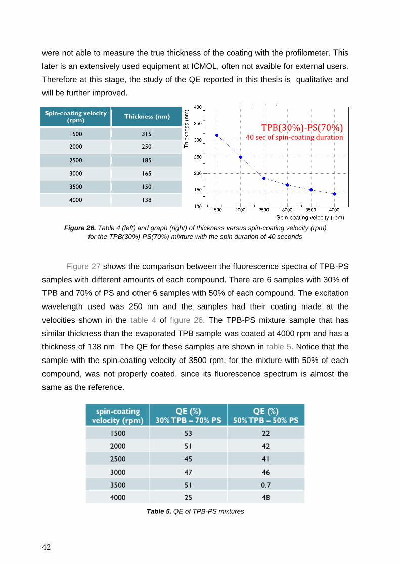
Figure 27 shows the comparison between the fluorescence spectra of TPB-PS
samples with different amounts of each compound. There are 6 samples with 30% of
TPB and 70% of PS and other 6 samples with 50% of each compound. The excitation
wavelength used was 250 nm and the samples had their coating made at the
velocities shown in the table 4 of figure 26. The TPB-PS mixture sample that has
similar thickness than the evaporated TPB sample was coated at 4000 rpm and has a
thickness of 138 nm. The QE for these samples are shown in table 5. Notice that the
sample with the spin-coating velocity of 3500 rpm, for the mixture with 50% of each
compound, was not properly coated, since its fluorescence spectrum is almost the
same as the reference.
Table 5. QE of TPB-PS mixtures
TPB(30%)-PS(70%) 40 sec of spin-coating duration
43
Figure 27. Fluorescence spectra of TPB(30%)-PS(70%) (left) and TPB(50%)-PS(50%) (right) mixtures
for six samples each with different spin-coating velocities, i.e. different thicknesses,
for the excitation wavelength of 250 nm
Figure 28 depicts the QE for the 4 samples with evaporated TPB for several
excitation wavelengths and the QE for 6 samples with TPB(30%)-PS(70%) for the
excitation wavelength of 250 nm. At the wavelength of 250 nm of the two samples, for
the thickness of ~135 nm we can see that the QE is much higher on the evaporated
sample than in the mixture, 49% against 25%. As for the samples with thicknesses
~150 nm the QE of the evaporated is 49% against 51% of the TPB-PS mixture. For
the thickness of ~260 nm the maximum QE value obtained for the evaporated sample
is 56% against 51% of the TPB(30%)-PS(70%) mixture. For higher coating
thicknesses above 140 nm, the QE of the TPB-PS mixture does not seem to depend
strongly on the coating thickness. This result is preliminary and should be further
confirmed with the determination of the error bars in the plot. The QE of the
evaporated TPB samples shown in figure 28-up appears to increase with the
wavelength reaching a maximum value of 77% at 370 nm and for a thickness of 260
nm. In figure 28-up we can also see that the QE of the evaporated TPB coating
increases with its thickness. Two samples of 260 nm thickness confirm the
consistency and repeatability of the result obtained.
44
Figure 28. (up) Conversion efficiency versus wavelength for 4 samples of evaporated TPB
and (bottom) conversion efficiency versus thickness for TPB(30%)-PS(70%) mixture with
40 seconds of spin-coating duration, for the excitation wavelength of 250 nm
The conversion efficiency versus the spin-coating velocity for the samples with
the TPB-PS mixture, is shown in figure 29. The spinning time for these mixtures was
40 seconds and an excitation wavelength of 250 nm was used for the QE
measurement. The sample with 50% proportion of TPB-PS coated at 3500 rpm had
an excitation spectrum compatible with the reference spectrum, giving a QE value
compatible with zero. This indicates a failure in the spin-coating process due either to
the spin-coating machine or to the operator. The process has to be repeated at this
velocity. We also notice from figure 29 that the QE for the 50%(TPB)-50%(PS)
mixture is slightly lower than the 30%(TPB)-70%(PS) mixture at the same thickness
(spinning velocity) and excitation wavelength. This is not what we expected as a
Evaporated TPB 4 Thicknesses
TPB(30%)-PS(70%) Spin-coating duration 40 s
Preliminary
45
larger proportion of TPB should produce a larger fluorescence yield. The two mixtures
have been prepared at different days and the slightly different preparation conditions
could have affected the fluorescence yield of the coatings. This also should be
confirmed by preparing the mixtures rigorously at the same time and conditions.
Figure 29. Conversion efficiency versus spin-coating velocity for TPB(30%)-PS(70%) (left)
and TPB(50%)-PS(50%) (right) mixtures with 40 seconds of spin-coating duration,
for the excitation wavelength of 250 nm
Figure 30 shows the fluorescence spectra and conversion efficiency of three
samples with a TPB(50%)-PS(50%) mixture, with different spin-coating duration and
800 rpm of spin-coating velocity. Once more, the excitation wavelength of 250 nm
was used. It can be seen in figure 30 that the QE improved compared to the samples
produced with a higher spin-coating velocity and it is basically constant within the
expected measurement errors. Indeed, the conversion efficiency at 40 seconds is of
53.6%, it is 54% at 50 seconds, and 53.9% at 60 seconds.
Figure 30. Fluorescence spectra (left) and conversion efficiency versus spin-coating duration (right)
of TPB(50%)-PS(50%) mixture, for three samples with different spin-coating duration
and 800 rpm of spin-coating velocity, for the excitation wavelength of 250 nm
TPB(30%)-PS(70%) 40 sec of spin-coating duration
TPB(50%)-PS(50%) 40 sec of spin-coating duration
TPB(50%)-PS(50%) 800 rpm of spin-coating velocity
Preliminary Preliminary
Preliminary
46
The coating quality and the QE obtained with the evaporated TPB were better
than the ones obtained with the TPB-PS mixtures using toluene as a solvent.
However, we cannot draw final conclusions at this stage, until the preparation
protocol of the TPB-PS mixtures is well established and understood. Also the QE
measurements should be improved by an analysis independent from the
spectrometer software. In particular, the statistical and systematic errors have to be
determined.
47
Chapter 3
Light transmission studies
The light transmission studies presented in this chapter are divided in two
major themes, the conductive and transparent coating for NEW and the light
transmission through the sapphire windows of the PMT cans.
The PMTs need to be protected by windows made with a material transparent
in the visible and strong enough to withstand the gas pressure. These windows have
to be coated with TPB. Transparent plates coated with TPB will be placed in front of
the SiPM tracking plane. Between the TPB and the substrate a conductive and highly
transparent layer has to be deposited in order to protect the windows from
accumulation of charges.
In addition to these different coatings on the sapphire window of the PMT cans,
an optical gel was considered for coupling the PMTs quartz window to the sapphire
window and so optimising the collection of light produced in the xenon for the energy
readout.
3.1. Conductive and transparent coatings in NEW
In NEW and NEXT-100 TPCs, the transparent plates in front of the SiPM
boards and the sapphire windows of the PMT cans will be coated with TPB, and prior
to it, a conductive and transparent coating should be applied to avoid accumulation of
charges and to screen the photosensors from the electric fields. The coatings should
be transparent in the blue range to maximize the number of photons that pass
through the protective windows and reach the photosensors. The windows will be
connected to the ground, through the conductive coatings.
48
The transparent and conductive materials considered will be chosen among
those tested and described in this section. The materials tested will be chosen for
their radiopurity, their high transmittance in the TPB emission range (350-650 nm),
their conductivity and good surface properties to be used as substrates for uniform
TPB coating.
For the purpose of achieving a good comparative study, the transmittance as a
function of wavelength of the windows and coatings and the conductivity of the
conductive coating materials, were measured. The materials considered to be used
as transparent windows in front of the SiPMs are: PMMA (Poly(methyl methacrylate)),
quartz and sapphire. This later material is used in the PMT cans because, in addition
to its known transparency, it has good mechanical properties that allow it withstand
high pressure. For the conductive and transparent coatings of the windows,
we have tested Au (Gold), ITO (Indium Tin Oxide), PEDOT-PSS
(Poly(3,4-ethylenedioxythiophene) - Poly(styrenesulfonate)) [42] and AgNW (Silver
Nanowires).
3.1.1. Transparent Materials for Windows
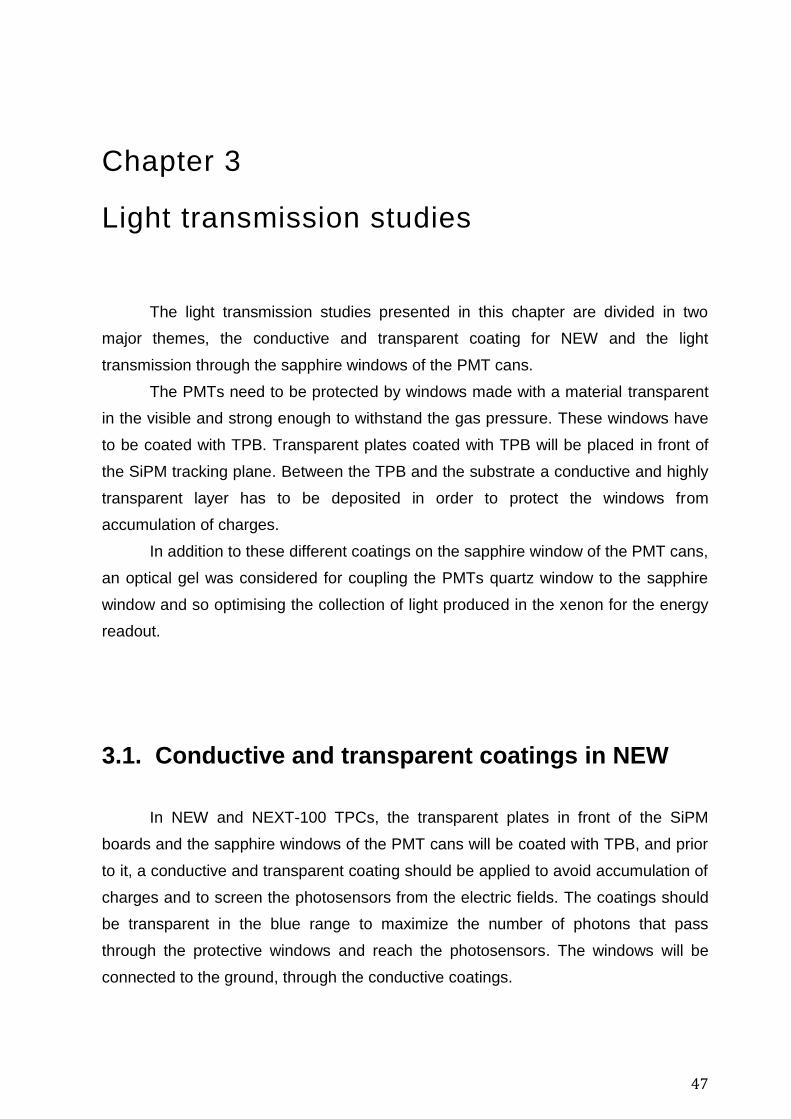
Unlike NEXT-DEMO, the silicon photomultipliers cannot be coated directly in
NEW and NEXT-100 because of the new design of the SiPM boards that form a
single piece with the Kapton cable for bias and signal (figure 31). The boards can no
longer be easily coated in the ICMOL evaporator. Instead, a transparent window,
appropriately coated, will be placed close in front of each board for the VUV light
conversion and shielding of the photosensors. These windows should be coated with
a high quality TPB deposition in order to insure a uniform VUV light conversion at
each SiPM of 1 mm2 active area, located close behind the window. The windows
material for the PMT cans has to be strong enough to resist the high pressure inside
the vessel. Sapphire was considered for its quite good mechanical properties that
allow them resist pressures of 15 bar without damage. It is furthermore highly
transparent in the visible range as shown later in figure 35. For the SiPMs windows,
PMMA, sapphire and quartz are being considered. The PMMA is cheaper but the
quartz and sapphire may allow a more uniform TPB coating because of their better
surface quality. Radiopurity of the materials is also an important issue for the final
49
choice that will be made. Screening of these materials is presently being made using
the germanium detectors of the Canfranc Laboratory. The initial choice of PMMA and
sapphire was based on the characteristics provided by the manufacturing Companies,
which are indicative. We have measured the transmittance precisely and in a wide
range of wavelengths.
Figure 31. Single piece SiPMs board with the Kapton cable
3.1.2. Transparent and Conductive Coatings
The purpose of the transparent and conductive materials, which will be used
on the windows prior to application of TPB, is to protect the photosensors from
accumulation of charges and from the electric fields. This coating has to be highly
transparent and conductive enough. The materials considered are: gold (Au), indium
tin oxide (ITO), an organic conductive material PEDOT-PSS, and silver nanowires
(AgNW), all for which we measured the transmittance as function of wavelength,
shown in figure 36.
The Au was applied by vacuum evaporation at ICMOL. The ITO was deposited
on the PMMA plates by vacuum evaporation produced by ECI Company [43]. Other
processes like etching or laser printing of ITO cannot be used on plastics because of
the heat produced in these processes that may damage these materials. The
standard cleaning protocol used at ICMOL for the substrate prior to TPB coating is:
50
alkaline soap, rinse with water, rinse with distilled water, ethanol or isopropanol, and
N2 drying. With this process the alcohol removed ITO evaporated on the PMMA
plates. This does not happen with ITO coated glass or quartz plates. The ITO-PMMA
plates cannot be cleaned according to the standard protocol necessary for high
quality depositions. Instead, they were cleaned only with distilled water, rinsed with
ethanol without scrubbing the surface, and dried with N2. Additionally, the surface was
treated with an oxygen plasma bath. This last step was necessary in order to activate
the surface to be coated with TPB, and so increasing its wetting property, i.e. its
ability to maintain the molecular contact with the material deposited on it and insuring
adherence and uniformity of the coating (figure 32). The coating with TPB on the ITO-
PMMA plates was made by vacuum evaporation with a coating thickness of 140 to
150 nm.
Figure 32. Wetting property: A – poor; B – medium; C – high. S – surface. (taken from Wikipedia)
An alternative to ITO is PEDOT-PSS, used in organic optoelectronic devices.
This is a conductive organic compound that can be acquired from Sigma-Aldrich in
aqueous solution. It is applied on the substrates by spin-coating. The process for
cleaning and deposition of PEDOT-PSS on quartz or sapphire begins with a standard
cleaning protocol followed by an oxygen plasma treatment. The deposition was made
by spin-coating (figure 33) with a precise monitoring of the parameters that determine
the thickness and quality of the coating: the spinning velocity, the spinning time, and
the positioning of the substrate using vacuum to fix and stabilize it on the spinner
plate. This spin-coating system is different from the one mentioned in the previous
chapter for the TPB QE measurement because the plates used here are larger. The
plate coated is then dried in an oven at 70 ºC.
51
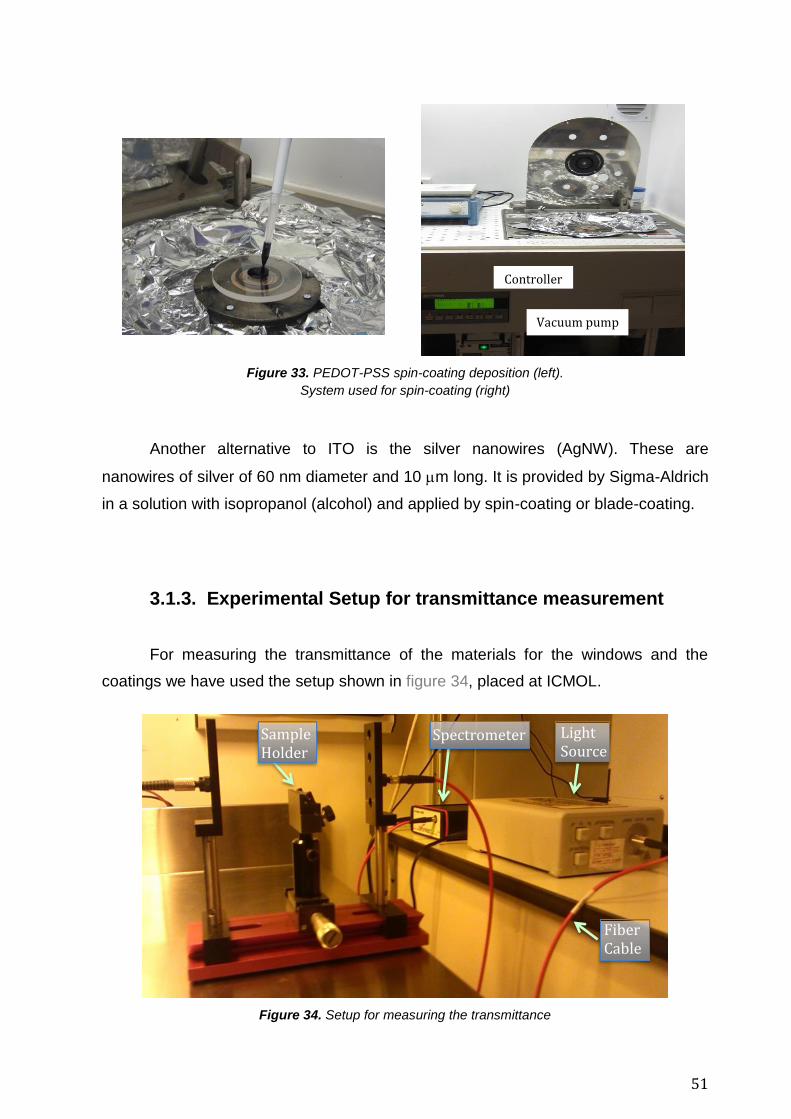
Figure 33. PEDOT-PSS spin-coating deposition (left).
System used for spin-coating (right)
Another alternative to ITO is the silver nanowires (AgNW). These are
nanowires of silver of 60 nm diameter and 10 m long. It is provided by Sigma-Aldrich
in a solution with isopropanol (alcohol) and applied by spin-coating or blade-coating.
3.1.3. Experimental Setup for transmittance measurement
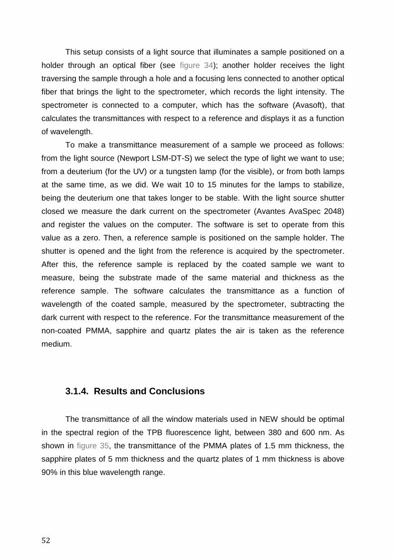
For measuring the transmittance of the materials for the windows and the
coatings we have used the setup shown in figure 34, placed at ICMOL.
Figure 34. Setup for measuring the transmittance
Vacuum pump
Controller
Light Source
Spectrometer Sample Holder
Fiber Cable
52
This setup consists of a light source that illuminates a sample positioned on a
holder through an optical fiber (see figure 34); another holder receives the light
traversing the sample through a hole and a focusing lens connected to another optical
fiber that brings the light to the spectrometer, which records the light intensity. The
spectrometer is connected to a computer, which has the software (Avasoft), that
calculates the transmittances with respect to a reference and displays it as a function
of wavelength.
To make a transmittance measurement of a sample we proceed as follows:
from the light source (Newport LSM-DT-S) we select the type of light we want to use;
from a deuterium (for the UV) or a tungsten lamp (for the visible), or from both lamps
at the same time, as we did. We wait 10 to 15 minutes for the lamps to stabilize,
being the deuterium one that takes longer to be stable. With the light source shutter
closed we measure the dark current on the spectrometer (Avantes AvaSpec 2048)
and register the values on the computer. The software is set to operate from this
value as a zero. Then, a reference sample is positioned on the sample holder. The
shutter is opened and the light from the reference is acquired by the spectrometer.
After this, the reference sample is replaced by the coated sample we want to
measure, being the substrate made of the same material and thickness as the
reference sample. The software calculates the transmittance as a function of
wavelength of the coated sample, measured by the spectrometer, subtracting the
dark current with respect to the reference. For the transmittance measurement of the
non-coated PMMA, sapphire and quartz plates the air is taken as the reference
medium.
3.1.4. Results and Conclusions
The transmittance of all the window materials used in NEW should be optimal
in the spectral region of the TPB fluorescence light, between 380 and 600 nm. As
shown in figure 35, the transmittance of the PMMA plates of 1.5 mm thickness, the
sapphire plates of 5 mm thickness and the quartz plates of 1 mm thickness is above
90% in this blue wavelength range.
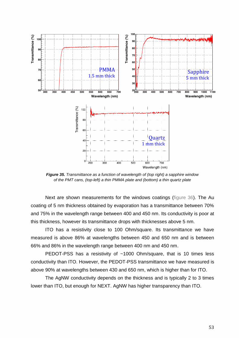
53
Figure 35. Transmittance as a function of wavelength of (top right) a sapphire window
of the PMT cans, (top-left) a thin PMMA plate and (bottom) a thin quartz plate
Next are shown measurements for the windows coatings (figure 36). The Au
coating of 5 nm thickness obtained by evaporation has a transmittance between 70%
and 75% in the wavelength range between 400 and 450 nm. Its conductivity is poor at
this thickness, however its transmittance drops with thicknesses above 5 nm.
ITO has a resistivity close to 100 Ohm/square. Its transmittance we have
measured is above 86% at wavelengths between 450 and 650 nm and is between
66% and 86% in the wavelength range between 400 nm and 450 nm.
PEDOT-PSS has a resistivity of ~1000 Ohm/square, that is 10 times less
conductivity than ITO. However, the PEDOT-PSS transmittance we have measured is
above 90% at wavelengths between 430 and 650 nm, which is higher than for ITO.
The AgNW conductivity depends on the thickness and is typically 2 to 3 times
lower than ITO, but enough for NEXT. AgNW has higher transparency than ITO.
PMMA 1.5 mm thick
Sapphire 5 mm thick
Quartz 1 mm thick
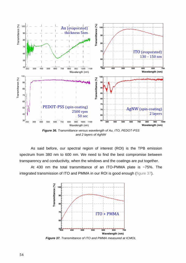
54
Figure 36. Transmittance versus wavelength of Au, ITO, PEDOT-PSS
and 2 layers of AgNW
As said before, our spectral region of interest (ROI) is the TPB emission
spectrum from 380 nm to 600 nm. We need to find the best compromise between
transparency and conductivity, when the windows and the coatings are put together.
At 430 nm the total transmittance of an ITO-PMMA plate is ~75%. The
integrated transmission of ITO and PMMA in our ROI is good enough (figure 37).
Figure 37. Transmittance of ITO and PMMA measured at ICMOL
Au (evaporated) thickness 5nm
PEDOT-PSS (spin-coating) 2500 rpm
50 sec
ITO (evaporated) 130 – 150 nm
AgNW (spin-coating) 2 layers
ITO + PMMA
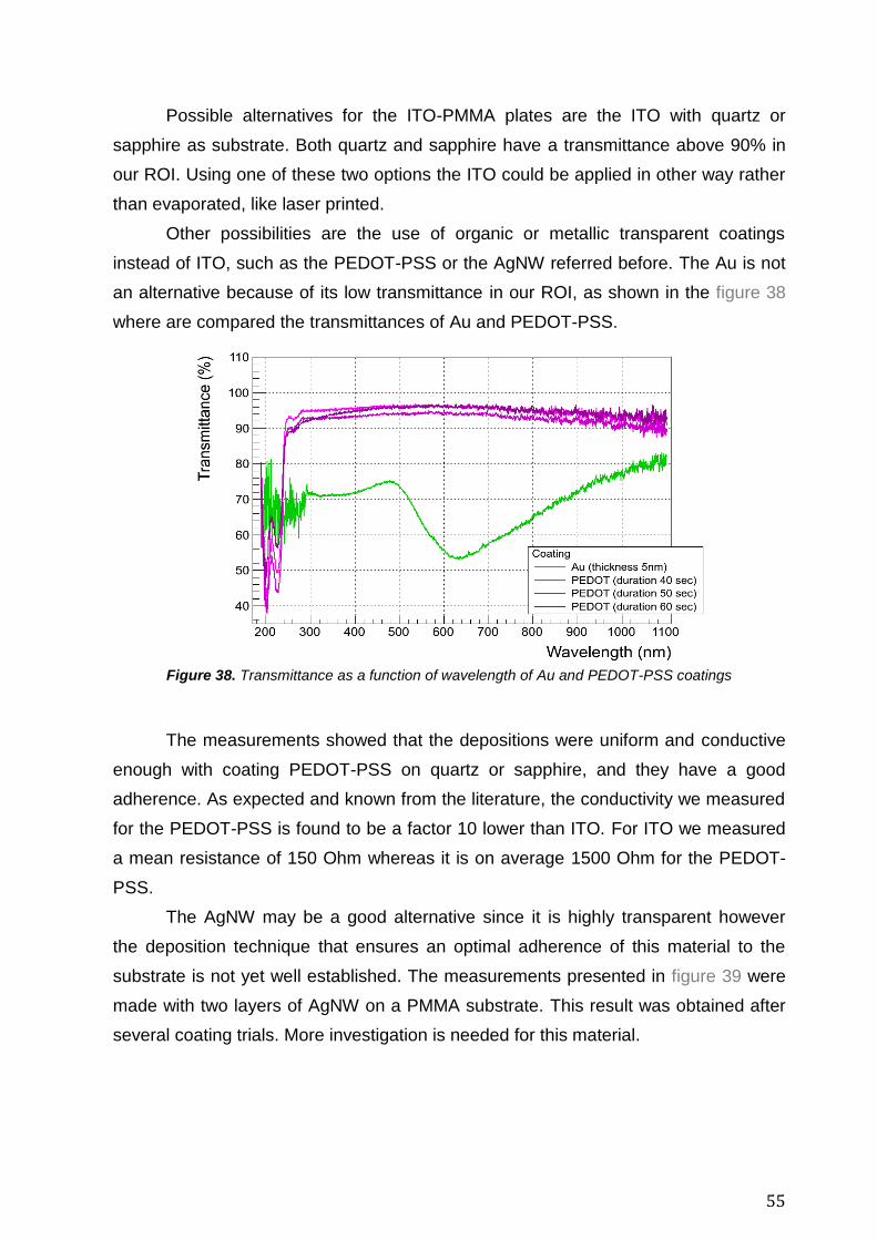
55
Possible alternatives for the ITO-PMMA plates are the ITO with quartz or
sapphire as substrate. Both quartz and sapphire have a transmittance above 90% in
our ROI. Using one of these two options the ITO could be applied in other way rather
than evaporated, like laser printed.
Other possibilities are the use of organic or metallic transparent coatings
instead of ITO, such as the PEDOT-PSS or the AgNW referred before. The Au is not
an alternative because of its low transmittance in our ROI, as shown in the figure 38
where are compared the transmittances of Au and PEDOT-PSS.
Figure 38. Transmittance as a function of wavelength of Au and PEDOT-PSS coatings
The measurements showed that the depositions were uniform and conductive
enough with coating PEDOT-PSS on quartz or sapphire, and they have a good
adherence. As expected and known from the literature, the conductivity we measured
for the PEDOT-PSS is found to be a factor 10 lower than ITO. For ITO we measured
a mean resistance of 150 Ohm whereas it is on average 1500 Ohm for the PEDOT-
PSS.
The AgNW may be a good alternative since it is highly transparent however
the deposition technique that ensures an optimal adherence of this material to the
substrate is not yet well established. The measurements presented in figure 39 were
made with two layers of AgNW on a PMMA substrate. This result was obtained after
several coating trials. More investigation is needed for this material.
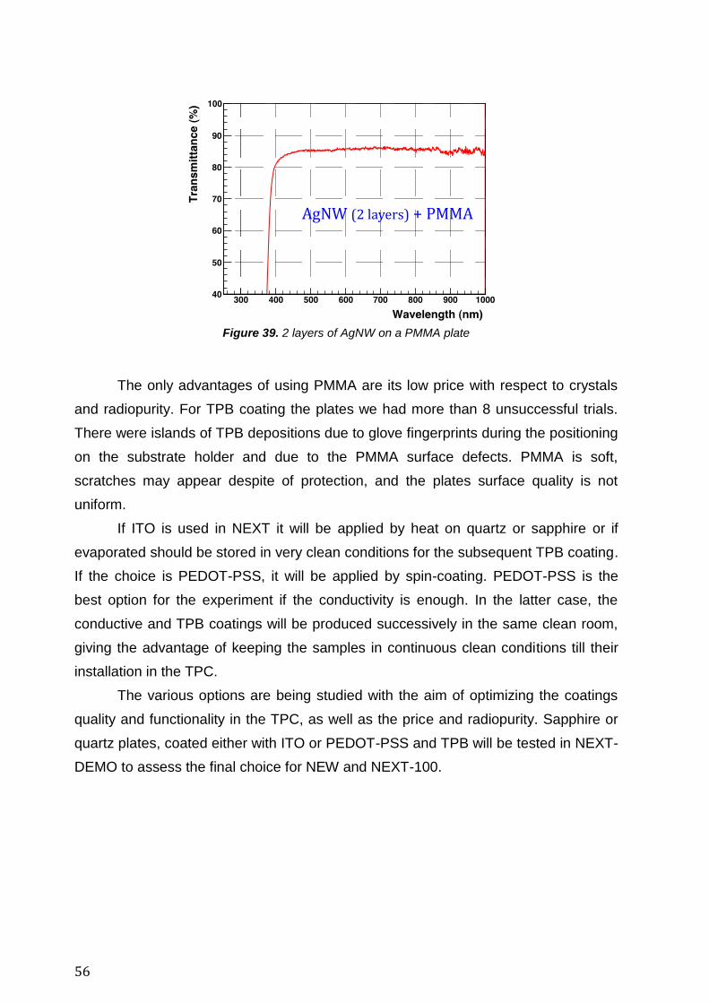
56
Figure 39. 2 layers of AgNW on a PMMA plate
The only advantages of using PMMA are its low price with respect to crystals
and radiopurity. For TPB coating the plates we had more than 8 unsuccessful trials.
There were islands of TPB depositions due to glove fingerprints during the positioning
on the substrate holder and due to the PMMA surface defects. PMMA is soft,
scratches may appear despite of protection, and the plates surface quality is not
uniform.
If ITO is used in NEXT it will be applied by heat on quartz or sapphire or if
evaporated should be stored in very clean conditions for the subsequent TPB coating.
If the choice is PEDOT-PSS, it will be applied by spin-coating. PEDOT-PSS is the
best option for the experiment if the conductivity is enough. In the latter case, the
conductive and TPB coatings will be produced successively in the same clean room,
giving the advantage of keeping the samples in continuous clean conditions till their
installation in the TPC.
The various options are being studied with the aim of optimizing the coatings
quality and functionality in the TPC, as well as the price and radiopurity. Sapphire or
quartz plates, coated either with ITO or PEDOT-PSS and TPB will be tested in NEXT-
DEMO to assess the final choice for NEW and NEXT-100.
AgNW (2 layers) + PMMA
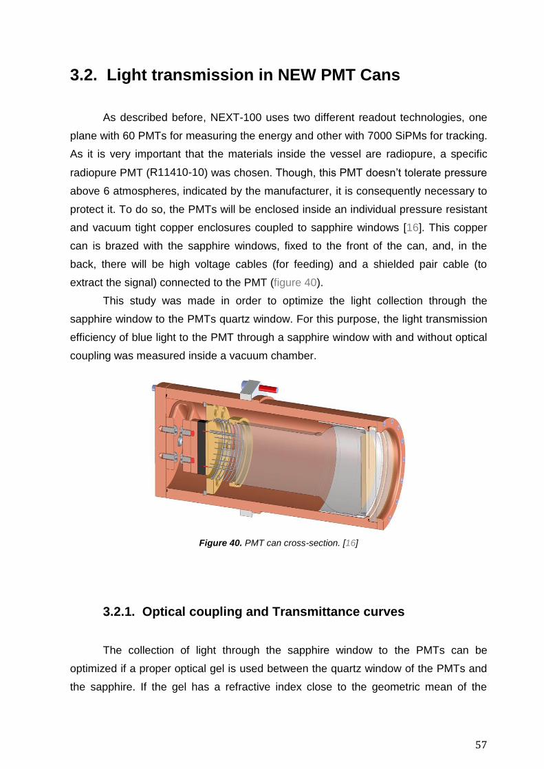
57
3.2. Light transmission in NEW PMT Cans
As described before, NEXT-100 uses two different readout technologies, one
plane with 60 PMTs for measuring the energy and other with 7000 SiPMs for tracking.
As it is very important that the materials inside the vessel are radiopure, a specific
radiopure PMT (R11410-10) was chosen. Though, this PMT doesn’t tolerate pressure
above 6 atmospheres, indicated by the manufacturer, it is consequently necessary to
protect it. To do so, the PMTs will be enclosed inside an individual pressure resistant
and vacuum tight copper enclosures coupled to sapphire windows [16]. This copper
can is brazed with the sapphire windows, fixed to the front of the can, and, in the
back, there will be high voltage cables (for feeding) and a shielded pair cable (to
extract the signal) connected to the PMT (figure 40).
This study was made in order to optimize the light collection through the
sapphire window to the PMTs quartz window. For this purpose, the light transmission
efficiency of blue light to the PMT through a sapphire window with and without optical
coupling was measured inside a vacuum chamber.
Figure 40. PMT can cross-section. [16]
3.2.1. Optical coupling and Transmittance curves
The collection of light through the sapphire window to the PMTs can be
optimized if a proper optical gel is used between the quartz window of the PMTs and
the sapphire. If the gel has a refractive index close to the geometric mean of the
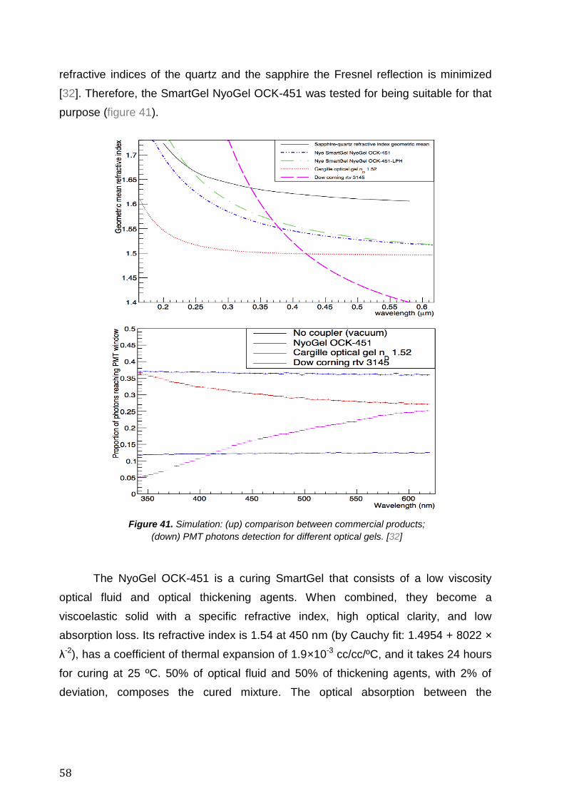
58
refractive indices of the quartz and the sapphire the Fresnel reflection is minimized
[32]. Therefore, the SmartGel NyoGel OCK-451 was tested for being suitable for that
purpose (figure 41).
Figure 41. Simulation: (up) comparison between commercial products;
(down) PMT photons detection for different optical gels. [32]
The NyoGel OCK-451 is a curing SmartGel that consists of a low viscosity
optical fluid and optical thickening agents. When combined, they become a
viscoelastic solid with a specific refractive index, high optical clarity, and low
absorption loss. Its refractive index is 1.54 at 450 nm (by Cauchy fit: 1.4954 + 8022 ×
λ-2), has a coefficient of thermal expansion of 1.9×10⁻³ cc/cc/ºC, and it takes 24 hours
for curing at 25 ºC. 50% of optical fluid and 50% of thickening agents, with 2% of
deviation, composes the cured mixture. The optical absorption between the
59
wavelengths of 400 nm and 750 nm is less than 0.001% micron, as depicted in figure
42.
Figure 42. Optical Clarity vs. Wavelength of the NyoGel OCK-451. [33]
The transmittance of the sapphire and of the SmartGel was measured using
the procedure described in the previous section. At the wavelength of 450 nm ± 20
nm the transmittance of the SmartGel is higher than for the sapphire. This means that
all the photons that pass through the Sapphire also pass through the SmartGel
because of its higher transmittance (figure 43).
Figure 43. Transmittance of sapphire (left) and NyoGel OCK-451 (right)
Sapphire
NyoGel OCK-451
60
3.2.2. Experimental Setup
In order to study the light transmission efficiency of blue light to the PMT,
through a sapphire window with and without optical coupling in a vacuum chamber,
the setup shown in figure 44 was used.
Figure 44. Vacuum chamber view and the equipment therein for testing the optical gel
The setup consists of a vacuum chamber connected to a primary and a turbo-
molecular vacuum pumps. Inside the chamber a blue LED (wavelength of 450 nm ±
20 nm) was placed and connected to a sourcemeter operating at a stable current of 3
mA. The LED illuminates the PTFE plane at a distance that ensures the uniformity of
the light detected by the PMT. The PMT, without gain (the first Dynode, Dy1, to the
Dy10 were at the same potential), was placed on a stand that simulates the copper
can, with the sapphire window in front. The PMT receives 240 V from a voltage
source, since it has optimal collection efficiency at this value (figure 10); it is also
connected to an electrometer.
In figure 45 it can be seen that the PMT current follows the trend of the LED
intensity as a function of its forward polarization current. Also, the PMT response is
linear in the whole emission of the LED. The illumination level of the LED has been
LED
PMT
PTFE
Vacuum Chamber
61
chosen low enough: polarization current equal to 3 mA to ensure linear response in
the PMT and far from its dark current regime.
Figure 45. (left) Typical performance curve (by the manufacturer).
(right) Measured PMT response (photocurrent vs. LED polarization current)
For the test using the gel, the SmartGel NyoGel OCK-451 was coupled
between the PMT quartz window and the sapphire. Several tests were made, among
which two required approximately 165 hours with increasing vacuum level. During the
tests the vacuum level ranged from 10 to 2.5×10⁻⁶ mbar and the room temperature
was at 23ºC.
3.2.3. Simulations
Simulations are necessary to understand the light transmission from the xenon
volume to the PMTs in their enclosures. For this we use Nexus, a GEANT4 based
software developed for the simulation of the NEXT TPC. We are presently working on
these simulations. This work is not completed yet and the results will be presented in
future reports.
62
3.2.4. Results and Conclusions
The PMT photocurrent with and without optical gel shows a major increase in
light yield using the SmartGel. Figure 46 shows three tests where the first two were
made over a period of 165 hours, and both follow the same trend. The third test is
useful for showing that these results are repeatable.
Figure 46. PMT photocurrent measured along the time with and without optical gel
From the next graphs (figures 47 and 48), the dependence of the PMT
photocurrent with the vacuum level is shown to be not very significative.
Figure 47. PMT photocurrent with the variation of the vacuum level, without gel.
Results for the three tests represented in the table 6
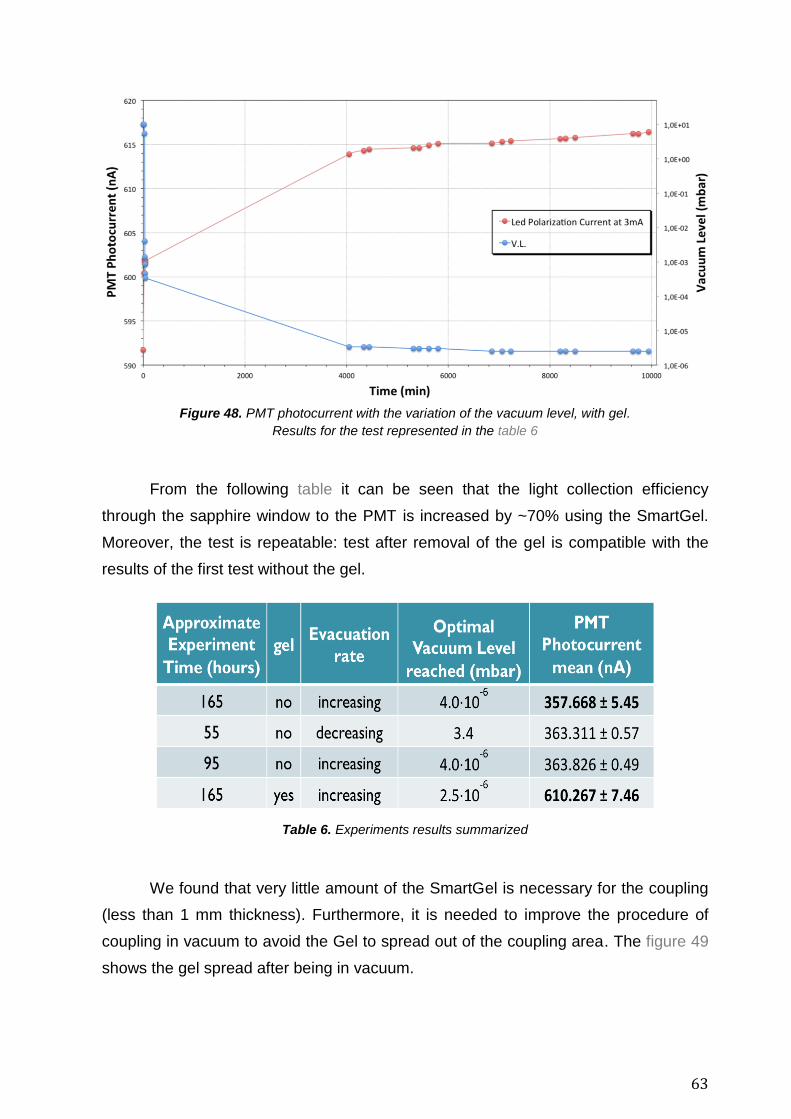
63
Figure 48. PMT photocurrent with the variation of the vacuum level, with gel.
Results for the test represented in the table 6
From the following table it can be seen that the light collection efficiency
through the sapphire window to the PMT is increased by ~70% using the SmartGel.
Moreover, the test is repeatable: test after removal of the gel is compatible with the
results of the first test without the gel.
Table 6. Experiments results summarized
We found that very little amount of the SmartGel is necessary for the coupling
(less than 1 mm thickness). Furthermore, it is needed to improve the procedure of
coupling in vacuum to avoid the Gel to spread out of the coupling area. The figure 49
shows the gel spread after being in vacuum.
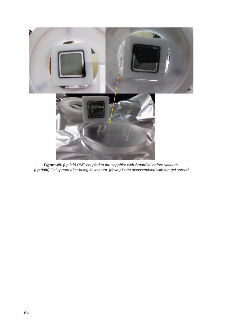
64
Figure 49. (up left) PMT coupled to the sapphire with SmartGel before vacuum.
(up right) Gel spread after being in vacuum. (down) Parts disassembled with the gel spread
65
Chapter 4
Summary and General Conclusions
The purpose of this master thesis was to contribute to the development of the
NEXT detector by studying EL light conversion and transmission.
For the first topic, light conversion, the SiPMs photodetection efficiency was
measured for three different SiPMs. The PDE measured at 285 nm using a linear fit to
the SiPM response curve at low illumination levels for the SiPM 1×1NC (1×1 mm2
non-coated) is PDE = 1.60 ± 0.01 %. As for the SiPMs coated with TPB we had an
increase of about a factor 9 compared to the non-coated SiPM. For the 1×1C (1×1
mm2 TPB-coated) SiPM, the PDE value measured is of 13.87 ± 0.04 % and for the
3×3C (3×3 mm2 TPB-coated) it is of 16.06 ± 0.12 %. These measurements were
intended to be made in the VUV range, unfortunately the monochromator used had a
vacuum leak that could not be solved in the span of this thesis schedule. The
monochromator was working properly, as proved by the tests made with a calibrated
PMT, but the vacuum was needed for reaching the 172 nm wavelength. The VUV
measurements will be completed in the near future after this vacuum leak is fixed.
As for the TPB quantum efficiency measurements different types of coatings
were tested in different conditions. It was demonstrated that the conversion efficiency
depends on the layer thickness and the way the coating is produced. For the samples
with TPB coated by evaporation the maximum QE obtained was 65% for the
thickness of 135 nm at the wavelength of 370 nm, 67% for the thickness of 150 nm at
the wavelength of 350 nm, 77% for the thickness of 260 nm at the wavelength of 370
nm. Comparing the TPB-PS mixtures coated by spinning we can realize that the QE
is higher in almost every case were the mixtures have 30% of TPB and 70% of PS
instead of 50% of each compound. The higher QE value of 53% obtained was for the
mixture with 30% of TPB and 70% of PS at 1500 rpm. This result was not expected
as for a larger amount of TPB in the mixture, a larger fluorescence yield is expected.
This situation can only be explained by the difference in the mixture preparation and
not by the amount of TPB. When the spin-coating is made at 800 rpm and compared
66
for 3 different coating durations for the mixture with 50% of TPB and PS, the QE
values obtained are very similar being the higher value 54% for the duration of 50
seconds.
For the second topic, light transmission, measurements of conductive and
transparent coatings were made. The materials for the windows and coatings were
considered for their transparency in the blue range. For the coatings the conductivity
was also measured. The materials considered for the windows, PMMA, sapphire and
quartz, have transmittance above 90% in the range between 380 and 600 nm. As for
the coatings, Au has the less transmittance, ~75%, and poor conductivity at 5 nm
thickness, thicker gold layers would be much less transparent. ITO has a
transmittance above 86% for wavelengths between 450 and 650 nm, and a resistivity
of ~100 Ohm/square. PEDOT-PSS has a resistivity of about 1000 Ohm/square and a
transmittance above 90%. AgNW has a transmittance above 95% in the blue region
and its conductivity is typically 2 to 3 times less than ITO, even so, good enough for
our purpose. However, its adherence to the substrate is not guaranteed using the
standard spin-coating deposition procedure. Putting together the windows and the
coatings materials, we obtained the results for our aim. At 430 nm the total
transmittance of an ITO-PMMA plate is ~75%. The alternatives to the ITO-PMMA
plates are the ITO on quartz or sapphire, these two materials having above 90%
transmittance in our ROI. We can also use PEDOT-PSS as a replacement of ITO if
we could prove with appropriate electrical tests that its conductivity is sufficient
enough for our application. The deposition of PEDOT-PSS has a good adherence. If
the conductivity is proved good enough, PEDOT-PSS would be the best option for
NEW. Gold coating is not an alternative because of its low transmittance.
As for the light transmission studies our aim was to see if we have advantage
in using a coupling gel to optimize the light collection efficiency of the PMTs in the
copper can with sapphire windows. We have tested the optical coupling gel during
~480 hours with varying the vacuum level. We found that using a small amount (less
than 1 mm of thickness) of the SmartGel we had an increase in the PMT photocurrent
of ~70%, without any decay over time; without gel we had a PMT photocurrent mean
of 357.67 ± 5.5 nA and with the gel this value was 610.27 ± 7.5 nA. Concerning the
application of the optical gel, we found that we need to improve the coupling
procedure in vacuum to avoid the spreading of the gel out of the coupling area.
In summary, we have managed to get results that may improve the collection
and transmission of the light from the xenon scintillation in the NEXT-White TPC.

67
More tests are needed to obtain more accurate results. Simulation studies for
comparison with the measurements are on progress and will be reported further.

68
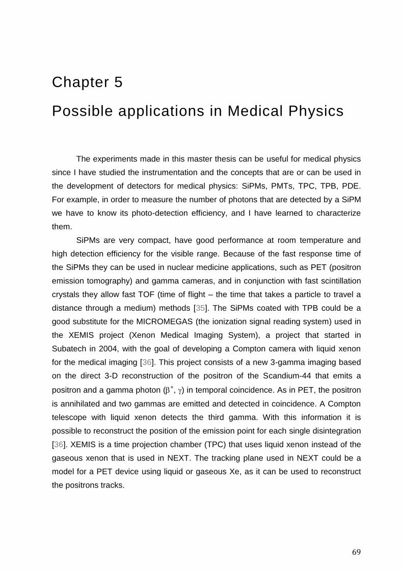
69
Chapter 5
Possible applications in Medical Physics
The experiments made in this master thesis can be useful for medical physics
since I have studied the instrumentation and the concepts that are or can be used in
the development of detectors for medical physics: SiPMs, PMTs, TPC, TPB, PDE.
For example, in order to measure the number of photons that are detected by a SiPM
we have to know its photo-detection efficiency, and I have learned to characterize
them.
SiPMs are very compact, have good performance at room temperature and
high detection efficiency for the visible range. Because of the fast response time of
the SiPMs they can be used in nuclear medicine applications, such as PET (positron
emission tomography) and gamma cameras, and in conjunction with fast scintillation
crystals they allow fast TOF (time of flight – the time that takes a particle to travel a
distance through a medium) methods [35]. The SiPMs coated with TPB could be a
good substitute for the MICROMEGAS (the ionization signal reading system) used in
the XEMIS project (Xenon Medical Imaging System), a project that started in
Subatech in 2004, with the goal of developing a Compton camera with liquid xenon
for the medical imaging [36]. This project consists of a new 3-gamma imaging based
on the direct 3-D reconstruction of the positron of the Scandium-44 that emits a
positron and a gamma photon (+, ) in temporal coincidence. As in PET, the positron
is annihilated and two gammas are emitted and detected in coincidence. A Compton
telescope with liquid xenon detects the third gamma. With this information it is
possible to reconstruct the position of the emission point for each single disintegration
[36]. XEMIS is a time projection chamber (TPC) that uses liquid xenon instead of the
gaseous xenon that is used in NEXT. The tracking plane used in NEXT could be a
model for a PET device using liquid or gaseous Xe, as it can be used to reconstruct
the positrons tracks.
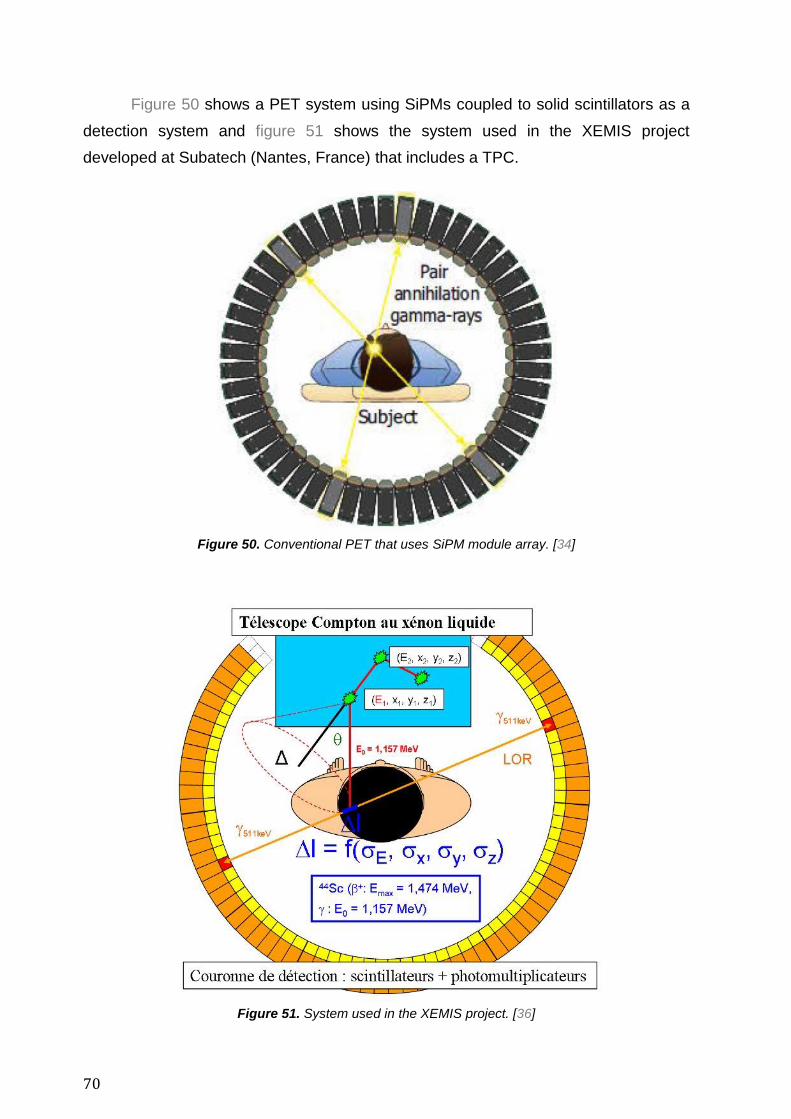
70
Figure 50 shows a PET system using SiPMs coupled to solid scintillators as a
detection system and figure 51 shows the system used in the XEMIS project
developed at Subatech (Nantes, France) that includes a TPC.
Figure 50. Conventional PET that uses SiPM module array. [34]
Figure 51. System used in the XEMIS project. [36]
71
Bibliography
[1] Max Planck Gesellschaft. "Neutrino". Glossary for the Research Perspectives of the Max Planck
Society. March 2012. http://www.mpg.de/12928/Glossary
[2] Alexandre Garcia. “Gaseous Mixtures/Detection Media Studies for NEXT Experiment: A
Contribution”. Dissertation presented to the Faculdade de Ciências e Tecnologia part of the
Universidade de Coimbra for a Master of Science Degree in Physics Engineering. September 2012.
[3] Calibration Instrumentation for CUORE in the Search for Neutrinoless Double Beta Decay.
http://www.astro.wisc.edu/~wolansky
[4] NEXT collaboration: V. Álvarez et al. “Design and characterization of the SiPM tracking system of
NEXT-DEMO, a demonstrator prototype of the NEXT-100 experiment”. JINST, vol. 8, no. T05002.
2013.
[5] David Nygren. “Optimal detectors for WIMP and 0−ν searches: Identical high-pressure xenon
gas TPCs?”. Nuclear Instruments & Methods in Physics Research A, 581(3):632–642. July 2007.
[6] M. Redshaw, E. Wingfield, J. McDaniel and E. Myers. “Mass and double-beta decay Q value of 136Xe”, Phys. Rev. Lett. 98 053003. 2007.
[7] Petr Vogel Steven R. Elliott. “Double beta decay”. Annual Review of Nuclear and Particle Science,
52:115151. December 2002.
http://dx.doi.org/10.1146/annurev.nucl.52.050102.090641
[8] Laboratorio Subterráneo de Canfranc. http://www.lsc-canfranc.es
[9] M. Fukugita and T. Yanagida. “Baryogenesis Without Grand Unification”, Phys. Lett. B174, 45.
1986.
[10] S. Davidson, E. Nardi, and Y. Nir. “Leptogenesis”, Phys. Rept. 466, 105–177. 2008.
[11] P. Minkowski. “µ → eγ at a rate of one out of 1-billion muon decays?”, Phys. Lett. B67, 421. 1977.
[12] R. N. Mohapatra and G. Senjanovic. “Neutrino Mass and Spontaneous Parity Violation”, Phys.
Rev. Lett. 44, 912. 1980.
[13] NEXT collaboration: Nadia Yahlali, L.M.P. Fernandes and David Lorca. “Characterization of UV-
enhanced SiPMs for Imaging in a High Pressure Xenon Electroluminescent TPC”.
[14] NEXT collaboration: V. Álvarez et al. “SiPMs coated with TPB: coating protocol and
characterization for NEXT”. JINST 7 P02010. 2012
[15] D. Nygren. “High-pressure xenon gas electroluminescent TPC for 0-ν decay search”. Nucl.
Instr. Meth. A, vol. 603, pp. 337–348. 2009.
72
[16] NEXT collaboration: J. Martín-Albo and J.J. Gómez-Cadenas. “Status and physics potential of
NEXT-100”. January 2013.
[17] “Operation and first results of the NEXT-DEMO prototype using a silicon photomultiplier tracking
array”. JINST 8 P09011. 2013
[18] NEXT collaboration: V. Álvarez et al., “NEXT-100 Technical Design Report (TDR). Executive
summary”, JINST, vol. 7, no. T06001. 2012.
[19] NEXT collaboration: V. Álvarez et al., “Initial results of NEXT-DEMO, a large-scale prototype of the
NEXT-100 experiment”, JINST, vol. 8, no. P04002. 2013.
[20] NEXT collaboration: V. Álvarez et al., “Near-Intrinsic Energy Resolution for 30 to 662 keV Gamma
Rays in High Pressure Xenon Electroluminescent TPC”, Nucl. Instr. Meth. A, vol. 708, pp. 101–114.
2013.
[21] NEXT collaboration: V. Álvarez et al., “Initial results of NEXT-DEMO, a large-scale prototype of the
NEXT-100 experiment”. JINST 8 P04002. 2013.
[22] F. Monrabal, A. Simón, J.J. Gómez-Cadenas. “Discovering neutrinoless double beta decay with
NEXT-100”, poster presented at the XV International Workshop on Neutrino Telescopes, Palazzo
Franchetti-Venice. March 2013.
[23] J.J. Gómez Cadenas. “The NEXT neutrinoless double beta decay experiment”. Presented at the
XV NEXT Collaboration Meeting. May 2014.
[24] NEXT collaboration: V. Álvarez et al., “Radiopurity control in the NEXT-100 0ν experiment:
procedure and initial measurements”. JINST, vol. 8, no. T01002. 2013.
[25] C.H. Lally, G.J. Davies, W.G. Jones, N.J.T. Smith, “UV quantum efficiencies of organic fluors”.
Nucl. Instrum. Meth. B, vol. 117, pp. 421. 1996.
[26] Lakowicz, J. R. “Principles of Fluorescence Spectroscopy (Third Edition ed.)”. (U. o. Medicine, Ed.)
Baltimore, Maryland, USA: Springer. 2006.
[27] RP Photonics. “Quantum Efficiency”. Retrieved from RP PhotonicsEncyclopedia
[28] “Absolute quantum yield measurement of solution using FP-8000 series“. JASCO
INTERNATIONAL CO., LTD.
[29] Greg McKee, L. I. “Integrating Spheres, Collecting and Uniformly Distributing Light”. Retrieved
from EDU.photonics.com
[30] Atsushi Kobayashi. “Absolute Measurements of Photoluminescence Quantum Yields of Organic
Compounds Using an Integrating Sphere”. Gunma University. 2010
[31] Hamamatsu. “Photonic Multichannel Analyzer”. Retrieved from hamamatsu.com
[32] NEXT collaboration: V. Álvarez et al., “Status report of the Energy plane subgroup of NEXT-NEW”.
May 2014.
[33] Nye SmartGels & Fluids Optical Coupling Technology. Retrieved from www.neyco.fr
73
[34] Hamamatsu. “MPPC modules technical information”. Retrieved from hamamatsu.com
[35] N. D’Ascenzo, V. Saveliev, Nuclear Instruments & Methods In Physics Research Section A (2011),
doi:10.1016/j.nima.2011.11.091
[36] Subatech. XEMIS project. http://www-subatech.in2p3.fr/en/research/nuclear-and-
health/xenon/research/applied/xemis/
[37] ICMOL, Instituto de Ciencia Molecular. http://www.icmol.es/
[38] KamLAND-Zen. http://www.awa.tohoku.ac.jp/kamlande/
[39] The EXO-200 Collaboration: J. B. Albert et al., “Search for Majorana neutrinos with the first two
years of EXO-200 data”. Nature. 2014. http://www-project.slac.stanford.edu/exo/
[40] Instituto de Fisica Corpuscular (IFIC). http://webific.ific.uv.es/web/
[41] Hamamatsu. http://www.hamamatsu.com
[42] F. Louwet et al, “PEDOT/PSS: synthesis, characterization, properties and applications”. Elsevier.
2002
[43] ECI evaporated coatings inc http://www.evaporatedcoatings.com/transparent-conductive-coatings

74
75
Acronyms Index
0: neutrinoless double beta
1×1C: 1×1 mm2 coated
1×1NC: 1×1 mm2 non-coated
2: two-neutrino double beta
3×3C: 3×3 mm2 coated
3-D: three-dimensional space
AgNW: silver nanowires
APD: avalanche photodiodes
Au: chemical symbol of gold
BC: blue configuration
BT-CCD: back-thinned charge-coupled
device
CCD: charge-coupled device
CERN: Conseil Européen pour la
Recherche Nucléaire (European
Organization for Nuclear Research)
EL: electroluminescence
EQE: external quantum efficiency
EXO: Enriched Xenon Observatory
FWHM: full width at half maximum
HPGXe: high-pressure gas xenon
HV: high voltage
ICMOL: Instituto de Ciencia Molecular
IFIC: Instituto de Física Corpuscular
IQE: internal quantum efficiency
ITO: indium tin oxide
KamLAND-Zen: Kamioka liquid
scintillator antineutrino detector
LBNL: Laurence Berkley National
Laboratory
LED: light-emitting diode
LSC: Laboratorio Subterráneo de
Canfranc
MPPC: multi-pixel photon counter
NEW: stands for NEXT-WHITE
NEXT: neutrino experiment with a
xenon time projection chamber
NEXT-100: NEXT with 100 kg of 136Xe
NEXT-DBDM: NEXT prototype
developed at LBNL for Dark Matter
and Double Beta Decay
NEXT-DEMO: NEXT demonstrator
NEXT-WHITE: NEXT detector named
in memoriam of Professor James
White from Texas University
PDE: photon detection efficiency
PEDOT-PSS: poly(3,4-
ethylenedioxythiophene) -
poly(styrenesulfonate)
PET: positron emission tomography
PMA: photonic multichannel analyser
PMMA: poly(methyl methacrylate)
PMT: photomultiplier
PS: polystyrene
PTFE: polytetrafluoroethylene, also
known as teflon
QCM: quartz crystal microbalance
QE: quantum efficiency
QY: quantum yield
ROI: region of interest
SiPM: silicon photomultiplier
SOFT: separated optimized function
76
TOF: time of flight
TPC: time projection chamber
TPB: tetraphenyl butadiene
TPB-PS: tetraphenyl butadiene -
polystyrene
UV: ultraviolet
UVC: ultraviolet configuration
V.L.: vacuum level
VUV: vacuum ultraviolet
XEMIS: xenon medical imaging system