Ligand Exchange Optimization for Quantum Dot Based ...
63
Master of Science Adviser: Paul Heremans, Full Professor, KU Leuven Co-adviser: Elvira Fortunato, Full Professor, NOVA University of Lisbon Tomás Correia Sanches Ligand Exchange Optimization for Quantum Dot Based Infrared Thin-film Photodetectors Dissertation submitted in partial fulfillment of the requirements for the degree of Master of Science in Micro and Nanotechnology Engineering April, 2021 Examination Committee ffChair: Prof. Rodrigo Martins sRapporteur: Prof. Hugo Águas Member: Prof. Paul Heremans
Transcript of Ligand Exchange Optimization for Quantum Dot Based ...

Master of Science
Adviser: Paul Heremans, Full Professor, KU Leuven
Co-adviser: Elvira Fortunato, Full Professor, NOVA University of Lisbon
Tomás Correia Sanches
Ligand Exchange Optimization for
Quantum Dot Based Infrared Thin-film
Photodetectors
Dissertation submitted in partial fulfillment
of the requirements for the degree of Master of Science in
Micro and Nanotechnology Engineering
April, 2021
Examination Committee
ffChair: Prof. Rodrigo Martins sRapporteur: Prof. Hugo Águas
Member: Prof. Paul Heremans

Ligand Exchange Optimization for Quantum Dot Based Infrared Thin-film Photodetectors

Ligand Exchange Optimization for Quantum Dot Based Infrared Thin-film Photodetectors
Ligand Exchange Optimization for Quantum Dot Based Infrared Thin-Film Photodetectors
Copyright © Tomás Correia Sanches, Faculty of Sciences and Technology, NOVA University Lisbon.
The Faculty of Sciences and Technology and the NOVA University Lisbon have the right, perpetual
and without geographical boundaries, to file and publish this dissertation through printed copies
reproduced on paper or on digital form, or by any other means known or that may be invented, and to
disseminate through scientific repositories and admit its copying and distribution for non-commercial,
educational or research purposes, as long as credit is given to the author and editor.

Ligand Exchange Optimization for Quantum Dot Based Infrared Thin-film Photodetectors
“Things only change when we change them.
But you have to do it.”
- Mikkel Nielsen

Ligand Exchange Optimization for Quantum Dot Based Infrared Thin-film Photodetectors

Ligand Exchange Optimization for Quantum Dot Based Infrared Thin-film Photodetectors
VI
Acknowledgments
First, I would like to express my greatest gratitude to my co-supervisor Professor Elvira Fortunato
for giving me the opportunity to perform my master thesis’ project at the world-leading research and
innovation hub in nanoelectronic, Imec. I am also grateful to my supervisor and President of the Imec
Department of Large Area Electronics, Professor Paul Heremans.
None of this would be possible without the dedication and commitment of Professor Rodrigo Martins
and Professor Elvira Fortunato, who together created the pioneering course of Micro and
Nanotechnologies Engineering.
A special appreciation to all Thin-film Photodetector group from Imec, (Dr. David Cheyns,
Dr. Pawel Malinowski, Bart, Vladimir, Griet, Itai, Luis, Myung-Jin) for allowing me to be part of a
group full of people with great minds, willing to help me from day one.
For all your patience, dedication, guidance, and knowledge, my mentor Dr. Epimitheas Georgitzikis,
known as Themis, a thank you is nowhere near enough for how much you contributed to this work.
For supporting me financially during my 7 months stay in Leuven, I am thankful to the program
Erasmus Plus.
Finally, I am extremely grateful to my friends and especially my family for all the support they have
always given me.

Ligand Exchange Optimization for Quantum Dot Based Infrared Thin-film Photodetectors
VII

Ligand Exchange Optimization for Quantum Dot Based Infrared Thin-film Photodetectors
VIII
Abstract
Image in the infrared wavelength range offers several advantages when compared with the visible
range. The information that is impossible to acquire with our naked eyes can be used for different
industries such as quality control, surveillance, augmented and virtual reality, medical diagnostics, and
others. Colloidal quantum dots (QDs) have been gathering increased attention and becoming one of the
most promising candidates for infrared optoelectronic devices, being praised for their size-dependent
bandgap tunability, low-cost manufacturing when comparing to III-V semiconductors, and suitability
for deposition on large and flexible substrates. However, the main challenge to accomplish is precise
control over their material properties through surface passivation.
The work performed in this thesis is focused on exploring the effect of different strategies of surface
ligand treatments to colloidal QDs for further integration as an active layer of thin-film photodetectors.
Therefore, thin-films made from solution-phase ligand exchange lead sulfide (PbS) QDs deposited on
glass substrates were analyzed in terms of their optical and morphological properties through multiple
characterization techniques. Full processing and fabrication of thin-film photodiode detectors were then
carried out, pursuing the highest devices performance according to their electrical characterization.
In the end, the developed PbS QD-based photodiode stack successfully completed the proposed
optimization by reaching dark currents values close to 10-5 A/cm2 at -3 V and external quantum
efficiency of 29% at 1450 nm.
Keywords: infrared, image sensor, colloidal quantum dots, ligands, thin-film, photodiode.

Ligand Exchange Optimization for Quantum Dot Based Infrared Thin-film Photodetectors
IX

Ligand Exchange Optimization for Quantum Dot Based Infrared Thin-film Photodetectors
X
Resumo
A imagem na gama de comprimento de onda infravermelho oferece várias vantagens quando
comparada com a gama visível. A informação que é impossível adquirir a olho nu pode ser utilizada
para diferentes indústrias, tais como controlo de qualidade, vigilância, realidade aumentada e virtual,
diagnósticos médicos e outros. Os quantum dots (QDs) coloidais têm vindo a despertar mais interesse
e a tornar-se um dos candidatos mais promissores para dispositivos optoelectrónicos infravermelhos,
sendo elogiados pela sua capacidade de sintonização do hiato energético dependente do tamanho, pelos
custos reduzidos de fabrico quando comparado com semicondutores III-V e pela aptidão para deposição
em substratos grandes e flexíveis. Contudo, o principal desafio a alcançar é o controlo preciso das suas
propriedades materiais através da passivação de superfície.
O trabalho realizado nesta tese centra-se na investigação do efeito de diferentes estratégias de
tratamentos ligantes na superfície de QDs coloidais para futura integração como camada ativa de
fotodetetores de filme fino. Por conseguinte, filmes finos feitos a partir de QDs de troca ligantes em
fase de solução de sulfureto de chumbo (PbS) depositados em substratos de vidro, foram analisados em
termos das suas propriedades óticas e morfológicas através de múltiplas técnicas de caracterização. O
processamento e fabrico completo de detetores fotodíodos de filme fino foi então levado a cabo, com o
intuito de obter o mais alto desempenho dos dispositivos de acordo com a sua caracterização elétrica.
No final, a arquitetura desenvolvida de fotodíodos baseada em QDs de PbS completou com sucesso a
otimização proposta, atingindo valores de correntes escura próximos de 10-5 A/cm2 a -3 V e uma
eficiência quântica externa de 29% a 1450 nm.
Palavras-chave: infravermelho, sensor de imagem, quantum dots coloidais, ligantes, filme fino,
fotodíodo.

Ligand Exchange Optimization for Quantum Dot Based Infrared Thin-film Photodetectors
XI
Ligand Exchange Optimization for Quantum Dot Based Infrared Thin-film Photodetectors
XII
Contents
Acknowledgments ........................................................................................................................... VI
Abstract ......................................................................................................................................... VIII
Resumo ............................................................................................................................................. X
List of Figures .............................................................................................................................. XIV
List of Tables ................................................................................................................................ XVI
Acronyms ................................................................................................................................... XVIII
Symbols ........................................................................................................................................... XX
1 Motivation and Objectives.......................................................................................................... 1
2 Introduction ................................................................................................................................ 3
2.1 Quantum dots basics ........................................................................................................... 3
2.2 Ligand exchange ................................................................................................................. 5
2.3 Solution-phase ligand exchange .......................................................................................... 7
3 Materials and Methods .............................................................................................................. 9
3.1 Substrates ............................................................................................................................ 9
3.2 Hole Transport Layer ........................................................................................................ 10
3.3 Active layer ....................................................................................................................... 10
3.4 Electron Transport Layer .................................................................................................. 11
3.5 Top Contacts Deposition ................................................................................................... 12
3.6 Characterization techniques .............................................................................................. 12
4 Results and Discussion ............................................................................................................ 13
4.1 Optimization of PbS QDs thin-films ................................................................................. 13
4.1.1 BTA:DMF-based thin-films ................................................................................................... 13
4.1.2 DFP-based thin-films ............................................................................................................. 16
4.1.3 Mercaptopropionic acid experiment....................................................................................... 18
4.1.4 Addition of Lead Chloride as a precursor .............................................................................. 20
4.1.5 Atomic Force Microscopy analysis ........................................................................................ 21
4.2 Photodiode fabrication and optimization .......................................................................... 22
4.2.1 Optimization of the p-type side of the junction ...................................................................... 23
4.2.2 Comparison between DFP and BTA:DMF ............................................................................ 29

Ligand Exchange Optimization for Quantum Dot Based Infrared Thin-film Photodetectors
XIII
4.2.3 Environmental conditions variations ...................................................................................... 30
5 Conclusions and Future Perspectives ..................................................................................... 33
Bibliography .................................................................................................................................... 35
Annexes ........................................................................................................................................... 39
A. Pictures of the BTA:DMF-based thin-films ...................................................................... 39
B. Pictures of the BTA:DFP and DFP-based thin-films ........................................................ 40
C. Comparation of final solutions with and without mercaptopropionic acid ....................... 41
D. Synthesis of quantum dots with the addition of lead chloride .......................................... 42

Ligand Exchange Optimization for Quantum Dot Based Infrared Thin-film Photodetectors
XIV
List of Figures
Figure 2-1: Schematics of nucleation and growth processes for: (a) hot-injection adapted from
[18], [19]; (b) heat-up methods adapted from [19], [20]......................................................................... 4
Figure 2-2: Absorption spectra of PbS colloidal QDs depending on their size [22].......................... 5
Figure 2-3: Energy shifts of CBM (green), VBM (black), Fermi level (red), and optical
bandgap (blue) using different ligands [25]. ........................................................................................... 6
Figure 2-4: Schematic diagram of the solid-state ligand exchange process [29]. .............................. 7
Figure 2-5: Schematic diagram of the solution-phase ligand exchange [29]. .................................... 7
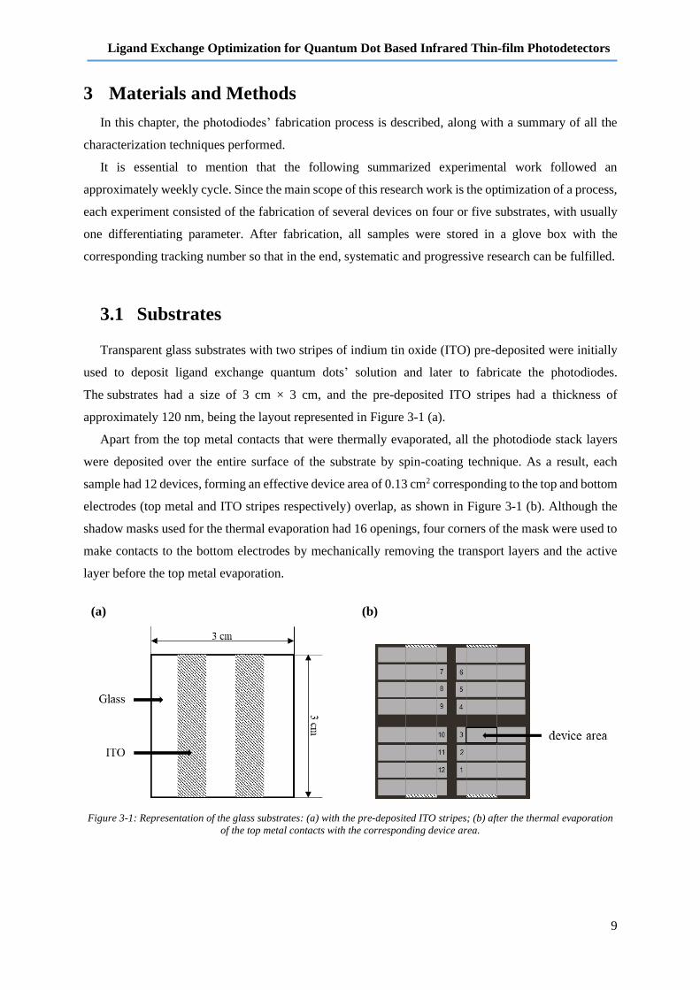
Figure 3-1: Representation of the glass substrates: (a) with the pre-deposited ITO stripes; (b) after
the thermal evaporation of the top metal contacts with the corresponding device area. ......................... 9
Figure 4-1: Optical Microscope analysis of thin-films using different ratios of solvents:
(a) 1BTA:1DMF; (b) 3BTA:1DMF; (c) 4BTA:1DMF; (d) 9BTA:1DMF. .......................................... 14
Figure 4-2: Photoluminescence analysis of thin-films using different ratios of solvents:
(a) Photoluminescence intensity vs. wavelength; (b) Normalized intensity vs. wavelength;
(c) Normalized intensity vs. time. ......................................................................................................... 15
Figure 4-3: Optical Microscope analysis of thin-films using different amounts and mixtures of
solvents: (a) 200 µl of DFP; (b) 250 µl of DFP; (c) Mixture of BTA with DFP. ................................. 16
Figure 4-4: Photoluminescence analysis of thin-films using different amounts and mixtures of
solvents: (a) Photoluminescence intensity vs. wavelength; (b) Normalized intensity vs. wavelength;
(c) Normalized intensity vs. time. ......................................................................................................... 17
Figure 4-5: Photoluminescence analysis of thin-films using an additional layer of MPA ligands with
different times of exchange (5, 10, 15, and 20 seconds): (a) Photoluminescence intensity vs. wavelength;
(b) Normalized intensity vs. wavelength; (c) Normalized intensity vs. time. ....................................... 19
Figure 4-6: Photoluminescence analysis of thin-films using an additional layer of ligands with
different times of exchange and a final annealing step: (a) Photoluminescence intensity vs. wavelength;
(b) Normalized intensity vs. wavelength; (c) Normalized intensity vs. time. ....................................... 20
Figure 4-7: AFM analysis of: DFP-based thin-film (a) and (b); BTA:DMF-based thin-film (c)
and (d). .................................................................................................................................................. 21
Figure 4-8: (a) Picture of the fabricated devices; (b) Schematic image of the device architecture
(stack) using PolyTPD hole transport layer, different ligand exchange PbS QDs approaches, and
titanium dioxide with niobium doping electron transport layer. ........................................................... 24
Figure 4-9: J-V curves for the 4 QDs (BDT ligands) layers sample. ............................................... 24
Figure 4-10: EQE curves for the 4 QDs (BDT ligands) layers sample: (a) EQE vs. Wavelength;
(b) EQE voltage dependency graph. ..................................................................................................... 25
Figure 4-11: Electrical characterization of the 2 QDs (BDT ligands) layers sample: (a) J-V curves;
(b) EQE voltage dependency graph and at the top right corner the EQE vs. Wavelength.................... 26
Ligand Exchange Optimization for Quantum Dot Based Infrared Thin-film Photodetectors
XV
Figure 4-12: Electrical characterization of the 1 QDs (BDT ligands) layer sample: (a) J-V curves;
(b) EQE vs. Wavelength. ...................................................................................................................... 26
Figure 4-13: Schematic image of the device architecture (stack) using nickel oxide hole transport
layer, solution-phase ligand exchange PbS QDs active layer, and titanium dioxide with niobium doping
electron transport layer. ........................................................................................................................ 27
Figure 4-14: J-V curves for the nickel oxide hole transport layer sample. ...................................... 28
Figure 4-15: EQE curves of the nickel oxide hole transport layer sample for two devices:
(a) EQE vs. Wavelength; (b) EQE voltage dependency graph. ............................................................ 28
Figure 4-16: Comparison of J-V curves for nickel oxide hole transport layer sample using
BTA:DMF (dark green) or DFP (orange). ............................................................................................ 29
Figure 4-17: Comparison of EQE curves for nickel oxide hole transport layer sample
using BTA:DMF (dark green) or DFP (orange): (a) EQE vs. Wavelength; (b) EQE voltage
dependency graph. ................................................................................................................................ 30
Figure 4-18: EQE curves under different conditions. ...................................................................... 31
Figure A-1: Thin-films fabricated based on BTA:DMF solvent. .................................................... 39
Figure B-2: Thin-films fabricated based on DFP and BTA:DFP solvent. ....................................... 40
Figure C-3: Final solution with the addition of mercaptopropionic acid. ........................................ 41
Figure C-4: Standard final solution before deposition (without mercaptopropionic acid). ............. 41
Figure D-5: Aggregation of particles formed during the synthesis. ................................................ 42

Ligand Exchange Optimization for Quantum Dot Based Infrared Thin-film Photodetectors
XVI
List of Tables
Table 4-1: Transient photoluminescence fitting results of the carrier lifetime with t1 representing the
fastest decay and t2 representing the slowest decay component for the different ratios of solvents. .... 15
Table 4-2: Transient photoluminescence fitting results of the carrier lifetime with t1 representing the
fastest decay and t2 representing the slowest decay component for different amounts and mixtures of
solvents. ................................................................................................................................................ 18
Table 4-3: EQE pick values under different conditions. .................................................................. 31

Ligand Exchange Optimization for Quantum Dot Based Infrared Thin-film Photodetectors
XVII

Ligand Exchange Optimization for Quantum Dot Based Infrared Thin-film Photodetectors
XVIII
Acronyms
3D
Three-dimensional
AFM
Atomic Force Microscopy
BDT Benzenedithiol
BTA
Butylamine
CMOS
Complementary Metal–Oxide–Semiconductor
DFP 2,6-difluoropyridine
DIW Deionized Water
DMF
N,N-dimethylmethanamide
EDT 1,2-ethanedithiol
EQE External Quantum Efficiency
ETL
Electron Transport Layer
FWHM
Full Width at Half Maximum
HTL Hole Transport Layer
HTP
4-hydroxythiophenol
IPA Isopropyl Alcohol
ITO
Indium Tin Oxide
LAE
Large Area Electronics
MA Malonic Acid
ME 2-mercaptoethanol
MPA
Mercaptopropionic Acid
NIR
Near-infrared
PL Photoluminescence
PolyTPD Poly[N,N'-bis(4-butylphenyl)-N,N'-bis(phenyl)-benzidine]

Ligand Exchange Optimization for Quantum Dot Based Infrared Thin-film Photodetectors
XIX
QDs
Quantum Dots
ROIC
Readout Integrated Circuits
SWIR
Short-wave Infrared
TEM Transmission Electron Microscopy
TFPD
Thin-film Photodetector
UV
Ultraviolet
XRD X-ray Diffraction

Ligand Exchange Optimization for Quantum Dot Based Infrared Thin-film Photodetectors
XX
Symbols
CdSe
Cadmium Selenide
ε
Dielectric constant
Jdark
Dark current density
NaAc Sodium Acetate
NiO
Nickel Oxide
PbBr2 Lead Bromide
PbCl2 Lead Chloride
PbI2 Lead Iodide
PbS Lead Sulfide
PbSe
Lead Selenide
Tbp Boiling point temperature
TiO2 Titanium Dioxide

Ligand Exchange Optimization for Quantum Dot Based Infrared Thin-film Photodetectors
XXI

Ligand Exchange Optimization for Quantum Dot Based Infrared Thin-film Photodetectors
1
1 Motivation and Objectives
Nowadays, almost all phones have at least two cameras, with a tendency for this number to grow
more and more. Imaging is becoming more than just taking pictures, it is becoming an acquisition of
information. The demand for examining objects and materials in a non-destructive way at higher
distances and under difficult lighting conditions is growing considerably in recent years.
The response has been directed to the infrared analyzes with different applications, namely facial and
gesture recognition, security surveillance, autonomous mobility, to name just a few, that need high
resolution imaging at low light levels, crucial for their implementation, being more accessible by having
a cheaper infrared technology.
Thin-film photodetectors (TFPD) technology appeared as an alternative to the conventional
fabrication of infrared sensors (flip-chip hybrid technologies). With a layer-by-layer approach, the new
technology opened a wide range of solution-processed materials, including colloidal QDs and a high
potential for large scale and low-cost integration on complementary metal-oxide-semiconductor
(CMOS) readout integrated circuits (ROIC).
TFPD group from Imec has been improving photodetectors performance to produce QDs sensors in
the infrared region that meet the industry demands. The work performed in this thesis is a continuation
of that track by optimizing a process focused on exploring the effect of different strategies of surface
ligand treatments to colloidal QDs. The results are expected to open up new possibilities for developing
colloidal quantum dot-based optoelectronic devices.
Full processing and characterization of thin-film photodetectors were carried out to achieve
photodiodes with the best electrical and optical performances. The prominent figures of merit of these
devices that will be studied are dark current density (Jdark) under reverse bias and External Quantum
Efficiency (EQE).

Ligand Exchange Optimization for Quantum Dot Based Infrared Thin-film Photodetectors
2

Ligand Exchange Optimization for Quantum Dot Based Infrared Thin-film Photodetectors
3
2 Introduction
2.1 Quantum dots basics
Over the past decades, considerable interest has been focused on small-sized (with diameters in the
range of 1-10 nm [1]) semiconducting nanoparticles named quantum dots (QDs). The interest was
unleashed by discovering of quantum size effects in 1981, stated by Ekimov and Onushchenko [2].
Due to this effect, they proved that by changing the size of QDs, it was possible to control the silicate
glass colour. Since then, the study of QDs has progressed significantly, resulting in implementations of
optoelectronic devices including light-emitting diodes [3]–[6], photodetectors [7]–[10], lasers [11], [12],
and solar cells [13], [14].
The synthesis of these particles is essential for their use in all these applications; otherwise, it is
impossible to guarantee precise control over their shape, structure, and size. A colloidal synthesis is a
wet-chemical approach involving precursor reagents and surfactant molecules/ligands that produce
colloidal QDs dispersed in solution. Thus, there are two common ways to prepare it: heat-up method [15]
and hot-injection [16].
One or more reactive precursors are rapidly injected into a high-temperature reaction solution in a
three-neck flask, as shown in Figure 2-1 (a), immediately starting the particles’ nucleation in the so-
called hot-injection method. The reaction solution contains a hot solvent and high boiling point
surfactant molecules/ligands to prevent QDs from agglomeration and provide good colloidal stability.
Due to the drop of precursor concentration because of particle formation and the drop of temperature
caused by the room temperature precursor(s) injection, the nucleation process is stopped, and particle
growth begins to occur. Different sizes, shapes, and compositions can be achieved by merely varying
the reaction time or temperature, the concentration of precursors, the ligands, among others showing
great flexibility for the use of several different materials and procedures [17].
Although hot-injection is the most common method used, some limitations make it challenging to
scale up for industrial productions. One example is the practicability and reproducibility of injecting
large volumes of solution. This process causes additional variations in the reaction conditions. It is
hugely affected by human factors, as it becomes impractical to inject such a quantity of solution, and
different users would always take different times to do so.
An alternative route is a heat-up based technique, also named the non-injection method. In contrast
to the method described above, all precursors and ligands are mixed at room temperature and then heated
up to initiate nucleation and consequent growth of QDs. The immediate conclusion is the greater
efficiency offered by this method since an injection step is no longer required.
The particle formation happens in a similar strategy to the hot-injection (rapid nucleation followed
by a slow growth process). Regardless, because of the overlap between the nucleation and growth stages,
as shown in Figure 2-1 (b), extended nucleation occurs, making it difficult to accomplish size uniformity.

Ligand Exchange Optimization for Quantum Dot Based Infrared Thin-film Photodetectors
4
Thereby, this method’s challenge is to choose the appropriate precursors and ligands along the correct
heating rate to tune the nucleation and growth rates, ensuring a narrow size distribution of particles while
maintaining colloidal stability [16].
(a)
(b)
Figure 2-1: Schematics of nucleation and growth processes for: (a) hot-injection adapted from [18], [19];
(b) heat-up methods adapted from [19], [20].
In addition to the great advantage that QDs can offer by enabling solution processing with low-cost
routes, simple deposition techniques (drop-casting, spin-coating, and dip-coating [19]), and easy
implementation for a variety of optoelectronic applications already mentioned, the quantum size effect
is a unique property of this particles resulted from the strong quantum confinement. When the size of
the particles is comparable to the excitation Bohr radius, defined by the natural length scale of the
electron and hole, confinement begins to affect the exciton wave function resulting in discrete energy
levels near the band edge and modifications in the energy level spacing (larger band gaps are obtained
as the particle size decreases) [21]. Hence, a large region of the visible spectrum can be achieved by
adjusting the bandgap of colloidal QDs through their size control. One example is the case of PbS QDs
demonstrated in Figure 2-2. By varying the dote size from 3 to 6 nm in diameter, the range from 800 nm
to 1700 nm, corresponding to near-infrared (NIR) and short-wave infrared (SWIR) can be selected,
becoming an attractive alternative for applications in different spectral zones.

Ligand Exchange Optimization for Quantum Dot Based Infrared Thin-film Photodetectors
5
Figure 2-2: Absorption spectra of PbS colloidal QDs depending on their size [22].
2.2 Ligand exchange
In complement to the control of the quantum dots’ physical properties, chemical processing,
including alloying and doping, ligand exchange, and core/shell formation, can also improve the
particles’ performance [19]. Focusing on ligand exchange, it is possible to produce, through surface
modification, a final thin-film with considerable improvements in the film properties and therefore in
device performance [23].
The most common ligands employed in QD synthesis are long-chain acid or amines molecules (with
length of ~2.5 nm [8]), used for passivating surface dangling bonds and making it possible to be
dispersed and stable in various solvents, including octane, toluene, and others. However, due to the
distance between the QDs being so long, a significant barrier to electron tunneling is emerged, affecting
the charge transport process [24]. To decrease the interparticle spacing, i.e., have the QDs tightly as
possible, shorter and more compact ligands are employed to replace the long organic ligands in a process
proclaimed ligand exchange.
The ability to change the conduction band minimum (CBM) and valence band maximum (VBM)
while maintaining a constant bandgap is another advantage that ligands offer [25]. Taking the example
of PbS QDs, 12 different ligands were tested by R. Brown et al. to study the energy level shifts of each
one using ultraviolet photoelectron spectroscopy (UPS) as shown in Figure 2-3. A maximum shift of
0.9 eV is observed, proving that ligand exchange is a way to achieve an ideal band alignment giving a
high degree of freedom in device engineering.
Everything has its drawbacks, and so these short ligands also have their own. Because of their small
size, they become volatile and vulnerable to oxidation, potentially causing degradation and instability
in device performance.

Ligand Exchange Optimization for Quantum Dot Based Infrared Thin-film Photodetectors
6
Figure 2-3: Energy shifts of CBM (green), VBM (black), Fermi level (red), and optical bandgap (blue) using different
ligands [25].
In general, ligand exchange can be performed either in the solid-state or in the solution-phase.
Since the solid-state procedure is adopted by many research groups and extensively exploited, a
variety of ligands were already tested, being methylamine, hydrazine, pyridine, and dithiols such as
1,2-ethanedithiol (EDT) and 1,4-benzenedithiol (BDT) among the ones of interest [26], [27].
The process begins with the deposition of colloidal quantum dots with the original ligands on top of
the substrate by typically using a small-scale physical deposition being spin-coating the technique used
in the present work. Subsequently, a solution containing short ligands is deposited on top of the film to
remove and replace the long ligands.
A passivated solid film is obtained after a short soaking period (usually no more than 10 seconds).
Typically, the final deposition is executed with a pure solvent, so the exchanged long ligands and excess
new short ligands can be removed. The final film’s thickness is controlled based on a layer-by-layer
approach by repeating the whole process previously detailed and demonstrated in Figure 2-4 until the
desired thickness is reached.
However, solid-state ligand exchange suffers from some drawbacks and limitations. An insufficient
exchange between the more extensive (original) ligands with the smaller ones can decrease the colloidal
stability and lead to poorly monodispersed particles [28]. Beyond the degraded passivation possibly to
happen, other problems with this method are the long fabrication time and the high material
consumption, making it an undesirable approach for large-scale manufacture [29].
Ligand Exchange Optimization for Quantum Dot Based Infrared Thin-film Photodetectors
7
Figure 2-4: Schematic diagram of the solid-state ligand exchange process [29].
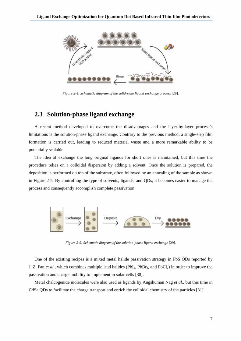
2.3 Solution-phase ligand exchange
A recent method developed to overcome the disadvantages and the layer-by-layer process’s
limitations is the solution-phase ligand exchange. Contrary to the previous method, a single-step film
formation is carried out, leading to reduced material waste and a more remarkable ability to be
potentially scalable.
The idea of exchange the long original ligands for short ones is maintained, but this time the
procedure relies on a colloidal dispersion by adding a solvent. Once the solution is prepared, the
deposition is performed on top of the substrate, often followed by an annealing of the sample as shown
in Figure 2-5. By controlling the type of solvents, ligands, and QDs, it becomes easier to manage the
process and consequently accomplish complete passivation.
Figure 2-5: Schematic diagram of the solution-phase ligand exchange [29].
One of the existing recipes is a mixed metal halide passivation strategy in PbS QDs reported by
J. Z. Fan et al., which combines multiple lead halides (PbI2, PbBr2, and PbCl2) in order to improve the
passivation and charge mobility to implement in solar cells [30].
Metal chalcogenide molecules were also used as ligands by Angshuman Nag et al., but this time in
CdSe QDs to facilitate the charge transport and enrich the colloidal chemistry of the particles [31].

Ligand Exchange Optimization for Quantum Dot Based Infrared Thin-film Photodetectors
8
Recently, a new ligand exchange strategy was reported by M. J. Choi et al. called cascade surface
modification achieving the highest power conversion efficiency in colloidal QDs solar cells (13.3%).
A step was added to the conventional method by performing a second surface modification
(re-exchange) on the short ligands. Functional ligands such as 2-mercaptoethanol (ME),
4-hydroxythiophenol (HTP), and malonic acid (MA) were employed to obtain better control of the
colloidal solubility and doping character of the QDs [32].
It is worth noting the fact that both methods of ligand exchange can be combined. Solution-phase
and solid-state treatments were conducted by Koleilat et al. in PbSe QDs, that were exchanged from
oleate ligand to shorter octylamine ligands (~1 nm) in solution. Then, films were fabricated by
spin-coating on glass substrates, using layer-by-layer processing and reaching ~110 nm of
thickness [33].
Ligand Exchange Optimization for Quantum Dot Based Infrared Thin-film Photodetectors
9
3 Materials and Methods
In this chapter, the photodiodes’ fabrication process is described, along with a summary of all the
characterization techniques performed.
It is essential to mention that the following summarized experimental work followed an
approximately weekly cycle. Since the main scope of this research work is the optimization of a process,
each experiment consisted of the fabrication of several devices on four or five substrates, with usually
one differentiating parameter. After fabrication, all samples were stored in a glove box with the
corresponding tracking number so that in the end, systematic and progressive research can be fulfilled.
3.1 Substrates
Transparent glass substrates with two stripes of indium tin oxide (ITO) pre-deposited were initially
used to deposit ligand exchange quantum dots’ solution and later to fabricate the photodiodes.
The substrates had a size of 3 cm × 3 cm, and the pre-deposited ITO stripes had a thickness of
approximately 120 nm, being the layout represented in Figure 3-1 (a).
Apart from the top metal contacts that were thermally evaporated, all the photodiode stack layers
were deposited over the entire surface of the substrate by spin-coating technique. As a result, each
sample had 12 devices, forming an effective device area of 0.13 cm2 corresponding to the top and bottom
electrodes (top metal and ITO stripes respectively) overlap, as shown in Figure 3-1 (b). Although the
shadow masks used for the thermal evaporation had 16 openings, four corners of the mask were used to
make contacts to the bottom electrodes by mechanically removing the transport layers and the active
layer before the top metal evaporation.
Figure 3-1: Representation of the glass substrates: (a) with the pre-deposited ITO stripes; (b) after the thermal evaporation
of the top metal contacts with the corresponding device area.
(a)
(b)

Ligand Exchange Optimization for Quantum Dot Based Infrared Thin-film Photodetectors
10
Concerning the substrates cleaning, the process started by hand washing the samples using deionized
water (DIW) with soap, followed by an ultrasonic bath under 50 °C of temperature for 5 minutes.
After the ultrasound with soap and DIW, the beaker where the samples were placed was put under
running water for 5 minutes since the soap must be entirely gone from the substrates. Afterwards, the
substrates went through several ultrasonic baths under the same temperature and duration mentioned
before, using different solvents in the following sequence (DIW, acetone, clean acetone, isopropyl
alcohol (IPA), and clean IPA). As final steps, substrates were dried with a nitrogen gun, and before the
deposition of the layers, a 5-minute oxygen plasma surface treatment was made.
3.2 Hole Transport Layer
Two different solutions used as hole transport layer (HTL) were tested during the devices’ fabrication
process. The first approach was made with an organic polymer named Poly[N,N'-bis(4-butylphenyl)-
N,N'-bis(phenyl)-benzidine], known as PolyTPD. The other material used was a solution of nickel oxide
(NiO) nanoparticles provided by Imec Thin-film Photodetectors group.
The solution preparation for PolyTPD started by removing the bottle kept in the freezer and leaving
it at room temperature for approximately 20 minutes. The next step was to dissolve the powder with
chlorobenzene to 6 mg/ml and kept it under stirring until no particles were detected (at least 30 minutes)
under an inert gas atmosphere (Jacomex GP(Concept) Glove Box / P(SYS) Inert Gas Purification
Module). After it, the filtration process was done with a glass syringe of 10 ml and a filter of 5 µm.
A magnet was added into the filtered solution, and it was kept on the stirring plate inside the glove box,
ready to be used in the next deposition. The solution’s deposition was also performed under an inert gas
atmosphere using a spin-coater (SPS-Europe Spin150 Spin Coater). Approximately 80 µl of the solution
were dropped on top of the substrate and immediately spun at 1000 rpm for 60 seconds, achieving a
thickness of 20 nm. The annealing of the film was executed at 150 °C for 20 minutes.
As for the nickel oxide, since the samples were supplied, the only necessary procedure to be done
before using it was an annealing process performed in air. To do so, a hot plate was used at its maximum
power until 300 °C degrees are reached. Only then the samples were placed on top of the plate.
After 30 minutes, the equipment is switched off, and when the 150 °C is reached the samples are taken.
3.3 Active layer
PbS QDs prepared by the solution-phase ligand exchange process using previously published
methods [34] were the infrared absorber material chosen to form the active layer of the devices produced
throughout this work. In total, 460 mg of lead iodide (PbI2), 74 mg of lead bromide (PbBr2), and 68 mg
of sodium acetate (NaAc) were mixed with 10 ml of N,N-dimethylmethanamide (DMF) and placed
under stirring until all the precursors were wholly dissolved. A 0.7 ml of QDs solution with a

Ligand Exchange Optimization for Quantum Dot Based Infrared Thin-film Photodetectors
11
concentration of 100 ml/mg was diluted in 9.3 ml of octane and put together with the precursors’ solution
after both being filtrated with a 0.1 µm filter. A vortex step was made to these hybrid solutions with a
IKA MS3 basic shaker at maximum speed until the QDs dispersed in DMF phase (around 10 minutes).
Hence, a phase separation happened, and the octane phase in the upper part of the vial is completely
removed with a pipette being replaced by 10 ml of clean octane as a washing step. The process was
repeated two more times to make sure that the remained original ligands were taken away. The obtained
PbS QDs in DMF phase were filtered with a 13 ml syringe through a 0.1 µm filter working as an
indication that the QDs were not aggregated with the ligand exchange happening properly. After that,
4 ml of toluene were mixed to precipitate the PbS QDs, being centrifuged for 2 minutes at 6000 rpm
and dried in vacuum for 3 minutes. Lastly, the quantity and the type of solvents chosen were added to
the solution, followed by a quick vortex step to redisperse the dots in the solvents. A final filtration with
a glass syringe of 10 ml and a 0.1 µm filter was done making the solution ready for deposition.
A solid-state ligand exchange was also performed below the solution-phase ligand exchange QDs
layer, and for that purpose, organic benzenedithiol (BDT) was dissolved with acetonitrile. Octane was
again used for dispersing PbS QDs and deposited by spin-coating under an inert environment. 30 μl of
the solution were dropped and immediately spun. A sufficient amount of stock solution was then
dropped to cover the whole substrate, followed by a break of at least 30 seconds so the shorter ligands
of BDT could replace the long oleic acid ligands. After this break, the same spin-coating conditions
have continued to be applied to dry the substrate and subsequently to wash it twice using pure
acetonitrile. These four spinning steps form a 30 nm thick layer, and for the desired thickness to be
accomplished, the process should be repeated the number of times needed.
3.4 Electron Transport Layer
The electron transport layer (ETL) solution used was always titanium dioxide nanoparticle solution
with 13% niobium doping (TiO2:Nb) previously synthesized by Imec Thin-film Photodetectors
group [35]. Before using it, the only procedure to be taken is to filter the solution with a 13 ml syringe
and a 0.1 µm filter. The solution’s deposition was carried out under an N2 environment with the help of
the spin-coater. Approximately 80 µl of the solution were dropped on top of the active layer and
immediately spun, achieving a thickness of 35 nm.

Ligand Exchange Optimization for Quantum Dot Based Infrared Thin-film Photodetectors
12
3.5 Top Contacts Deposition
Angstrom Åmod Deposition System was used for the thermal evaporation deposition of the top metal.
The shadow masks previously mentioned were aligned perpendicular to the ITO stripes as shown in
grey in Figure 3-1. Thus, aluminum was deposited on top of the ETL with a deposition rate of 3 Å/s
resulting in a thickness of 150 nm.
3.6 Characterization techniques
Atomic Force Microscopy (AFM) measurements were done on tapping mode with a Bruker Atomic
Force Microscope Dimension Edge Scanner, to obtain a morphological analysis of the thin films
produced using the ligand exchange quantum dots’ solution. Optical microscope images were taken to
observe the surface of these films and analyze possible defects and anomalies. The optical properties
were also studied by photoluminescence (PL) measurements using a Hamamatsu compact NIR PL
lifetime spectrometer C12132 series exciting the QDs film by a 532 nm laser. Profiler measurements
were made in contact mode with a Bruker DEKTAK XT Stylus Profiler to discover the active layer’s
thickness of the (for the devices) or just the thin-films.
Beyond the thin-film characterization, electrical characterization measurements of the devices
produced in this work were done through two techniques: Current-Voltage (I-V) and External Quantum
Efficiency (EQE) measurements.
I-V characterization was conducted in a glove box with a probe station coupled with a measurement
system Agilent HP 4155C Semiconductor Parameter Analyzer under dark conditions and simulated
solar light under AM1.5G conditions. The range voltage applied to the devices was from -3 V to 3 V
with a 0.01 V step and an active area of 0.13 cm2. To obtain the current density versus voltage curves
(J-V), the measured current values were divided by the active area and then plotted on a semi-
logarithmic graph, so it is possible to check low dark current density values.
The EQE measurements were performed with a setup composed of a lamp (Bentham
IL1 Illuminator/Bentham 610 Current Stablished Lamp Power Supply), a monochromator (LOT
Quantum Design Monochromator MSH-300), a frequency chopper (Bentham 418 USB Optical Chopper
Controller), a lock-in amplifier (Stanford Research Systems Lock-In Amplifier Model SR810 DSP),
and a preamplifier (Stanford Research Systems Low-Noise Current Preamplifier Model SR570).
The monochromator was set to a visible wavelength (555 nm) to align the sample, and a germanium cell
was used to calibrate the equipment. An N2 sealed sample mount was used to avoid ambient exposure
of the sample during the characterization. The wavelength range chosen for the measurements was from
1100 nm to 1700 nm with a 10 nm step under a constant bias of -3 V. Another EQE measurement was
done keeping constant the wavelength (corresponding to the highest EQE value for each device - mostly
1450 nm) and using voltage values from 0.5 V to -3 V with a 0.1 V step.
Ligand Exchange Optimization for Quantum Dot Based Infrared Thin-film Photodetectors
13
4 Results and Discussion
The present chapter is divided into two sections: optimization of PbS QDs thin-films and photodiode
fabrication and optimization. The experimental work started with an investigation of thin-films with
different ligand exchange options described in the first section to accomplish the best surface passivation
possible.
The second section is dedicated to the fabrication and characterization of photodiodes, being the
short-wavelength infrared the region of interest, especially wavelengths close to 1450 nm.
Over the experimental work multiple, materials and process parameters were tested to achieve the
required optimization and improve the devices operation.
4.1 Optimization of PbS QDs thin-films
Thin-films were made of solution-phase ligand exchange PbS QDs and deposited on top of glass/ITO
substrates using spin-coating technique under an inert atmosphere. In the end, the film’s thickness should
be thick enough to absorb all the incident light but, on the other hand, not too thick (more than 500 nm);
otherwise becomes improper for the extraction of chargers. Hence, a balance between absorption and
carrier transportation is necessary to secure in order to obtain an optimal thickness with literature settling
values between 200 nm and 400 nm [24], [36], [37].
To compare the results, the processing steps to passivate the QDs were kept the same for all the
samples while only changing the solvent used as a final step to disperse and stabilize the particles.
4.1.1 BTA:DMF-based thin-films
A mixture of butylamine (BTA) with DMF was used as the solvent (following the reported procedure
of the article on which the preparation of the PbS QDs was based [34]), testing different ratios but
maintaining the same total amount of solvents (200 µl). Equal proportions of both solvents were tested,
and a higher quantity of BTA compared to DMF in ratios of 3:1, 4:1, and 9:1 with pictures of the results
after deposition being demonstrated in Figure A-1 of Annexes chapter.
The images taken from the optical microscope are shown in Figure 4-1, and it was evident that,
regardless of the proportion of solvents used, all the samples presented low film quality.
Poor morphology and numerous particle aggregations can be easily detected, especially in the sample
with the highest amount of BTA, which is adverse for the devices’ stability.

Ligand Exchange Optimization for Quantum Dot Based Infrared Thin-film Photodetectors
14
(a)
(b)
(c)
(d)
Figure 4-1: Optical Microscope analysis of thin-films using different ratios of solvents:
(a) 1BTA:1DMF; (b) 3BTA:1DMF; (c) 4BTA:1DMF; (d) 9BTA:1DMF.
With the aid of a profilometer, the thickness of the films was measured. Despite the different ratios,
due to the same total amount of solvents and the same spin-coating conditions at deposition (1500 rpm
for 30 seconds), all the samples were close to 325 nm, which are acceptable values based on literature.
The photoluminescence analysis results are shown in Figure 4-2 with the ratio of 3BTA to 1DMF
(red line) ensuring the best results overall. Besides having the highest exciton peak with 109580 counts
(which is more than 20% than the other two samples) for the wavelength of 1485 nm determine by
Figure 4-2 (a), it is the ratio that has the highest carrier lifetime by inspection of Figure 4-2 (c) and
proven by the values in Table 4-1.
Even though all the samples tested had their peak position at 1485 nm, which is close to the
wavelength of interest for this work, different values of full width at half maximum (FWHM) were
revealed. Calculated by the difference between the low and high wavelength values at half spectral
maximum intensity, the FWHM value should be as low as possible to ensure homogeneous and
monodisperse films.
The narrowest excitation peak and consequently the lowest FWHM belong to the sample with a ratio
of 9 to 1 (green line) once it obtained a value of 119 nm, followed by the 3BTA:1DMF sample with
133 nm and lastly, the sample corresponding to the mixture of the same amount of solvents (blue line)
that reached 141 nm. This comparison was made based on the graph of Figure 4-2 (b) since it presents
a y-axis with normalized intensity values. Although it did not obtain the best value of FWHM, because
of the remaining photoluminescent analysis and the optical microscopic images, the ratio of 3BTA to
1DMF was chosen as the best conditions to continue.

Ligand Exchange Optimization for Quantum Dot Based Infrared Thin-film Photodetectors
15
(a)
(b)
(c)
Figure 4-2: Photoluminescence analysis of thin-films using different ratios of solvents:
(a) Photoluminescence intensity vs. wavelength; (b) Normalized intensity vs. wavelength; (c) Normalized intensity vs. time.
Table 4-1: Transient photoluminescence fitting results of the carrier lifetime with t1 representing the fastest decay and
t2 representing the slowest decay component for the different ratios of solvents.
Ratio of solvents t1 (ns) t2 (ns)
3BTA:1DMF 34.23 308.15
1BTA:1DMF 26.96 244.51
9BTA:1DMF 12.03 169.65

Ligand Exchange Optimization for Quantum Dot Based Infrared Thin-film Photodetectors
16
4.1.2 DFP-based thin-films
Another solvent tested was 2,6-difluoropyridine (DFP) previous reported by Qianglu et al. [27] with
results of homogeneous and good dispersibility thin-films. Combining a relatively low boiling point
(Tbp = 124 °C) and a high dielectric constant (ε = 107.8), this polar solvent promises complete redisperse
QDs with minimal dot aggregation.
In fact, the better film quality was revealed by the images taken from the optical microscope (Figure
4-3 (a) and (b)). Two samples were fabricated with different amounts of DFP (one with 200 µl and the
other with 250 µl), and both presented almost no aggregations and excellent uniformity.
BTA is commonly used as a solvent, but it is also known to act as a ligand, which may help the
passivation of QDs. Nevertheless, by mixing 200 µl of BTA with 50 µl of DFP, a huge color difference
between the other two samples was immediately noticeable after deposition (visible in Figure B-2 of
Annexes chapter) with the optical microscope images proven the film was full of cracks and defects
(Figure 4-3 (c)).
(a)
(b)
(c)
Figure 4-3: Optical Microscope analysis of thin-films using different amounts and mixtures of solvents:
(a) 200 µl of DFP; (b) 250 µl of DFP; (c) Mixture of BTA with DFP.
In terms of films’ thickness, much thinner films (less than 100 nm) were revealed. It is possible to
increase their thickness by adjusting some deposition parameters such as spin speed, duration, and rate
or even solution concentration. Thus, some modifications had to be made so the appropriate thickness
could be reached.

Ligand Exchange Optimization for Quantum Dot Based Infrared Thin-film Photodetectors
17
The results of the photoluminescence analysis of the DFP-based thin-films were presented alongside
the best results of the mixture of BTA with DMF to compare both attempts. Even though the
measurements were made using the same equipment and under the same conditions, this comparison
cannot be made for the peak intensity values due to the difference of thicknesses highlighted above.
Consequently, only the results of the two DFP-based films are shown in Figure 4-4 (a) being the sample
with the lowest amount (gold line), the one that achieves the highest peak intensity.
Concerning the wavelength corresponding to the peak intensity, both samples exhibit the same value
(1495 nm), which is higher than the 1485 nm previously referenced for the 3BTA:1DMF film noticeable
in Figure 4-4 (b) by the shift of the curves. Considering the same graph, it was possible to note that the
FWHM for both DFP-based films were nearly the same (141 nm) and slightly above the value reached
by the sample being compared (133 nm). To conclude, a significant difference in the charge carrier
lifetime values is shown by Figure 4-4 (c) and demonstrated in Table 4-2. This difference is possible to
justify by the previously mention double function of BTA. In principle, by working as an extra ligand
for the passivation, the BTA-based thin films are likely to have a better passivation, which leads to fewer
recombination and, therefore, longer carrier lifetime values.
(a)
(b)
(c)
Figure 4-4: Photoluminescence analysis of thin-films using different amounts and mixtures of solvents:
(a) Photoluminescence intensity vs. wavelength; (b) Normalized intensity vs. wavelength; (c) Normalized intensity vs. time.

Ligand Exchange Optimization for Quantum Dot Based Infrared Thin-film Photodetectors
18
Table 4-2: Transient photoluminescence fitting results of the carrier lifetime with t1 representing the fastest decay and
t2 representing the slowest decay component for different amounts and mixtures of solvents.
Solvents used t1 (ns) t2 (ns)
200 µl DFP 10.24 67.56
250 µl DFP 11.64 67.11
3BTA:1DMF 34.23 308.15
4.1.3 Mercaptopropionic acid experiment
The quality of the thin-films’ surface passivation is essential to determine the efficient transport of
the carriers. In that sense, a multiple passivation strategy was attempted using mercaptopropionic acid
(MPA) as part of the solution-phase ligand exchange and as an additional layer. The results of including
additional ligands by merely adding them to the solution were discouraging as they led to quantum dot
aggregation (observable by the pictures presented in section C of Annexes chapter), making it
impossible to perform the final filtration before deposition. A solid-state approach was taken by
depositing an MPA layer (2500 rpm for 30 seconds) on top of the solution ligand exchange QDs with
two different process parameters being investigated.
The first focus of the experiment was the time of exchange. After deposition of the MPA layer,
different times were taken until the sample is rotated, ensuring four different times with a range of
5 seconds for the particles soak the new ligands. Figure 4-5 shows the photoluminescence results
inferring that the strategy had insignificant results.
Contrary to stated results by Gu Mengfan et al. [38], the peak position (Figure 4-5 (b)) and the
lifetime values collected (Figure 4-5 (c)) were the same for the sample with just the layer of QDs and
for all the samples with the additional MPA layer. Moreover, all FWHM values were close to 123 nm,
and except from the sample without the MPA layer (blue line Figure 4-5 (a)) that showed the lowest
result (121.39 nm), the difference between the other values is insignificance. Out of all the analysis
made and comparing all the samples with an MPA layer and the sample without it, only an increase of
the peak intensity was evident through Figure 4-5 (a).

Ligand Exchange Optimization for Quantum Dot Based Infrared Thin-film Photodetectors
19
(a)
(b)
(c)
Figure 4-5: Photoluminescence analysis of thin-films using an additional layer of MPA ligands with different times of
exchange (5, 10, 15, and 20 seconds): (a) Photoluminescence intensity vs. wavelength;
(b) Normalized intensity vs. wavelength; (c) Normalized intensity vs. time.
The other process parameter examined was the impact of a final annealing of the films during
5 minutes at 80 °C while reproducing all the procedures performed before. It is expected that through
the post-annealing process, the residual organic ligands can be removed, helping the enhancement of
conductivity and charge carrier mobility. It also might help to attain more compact and energetically
rearranged films.
Starting the evaluation of the photoluminescence measurements with the graph of Figure 4-6 (a),
once again, a higher peak intensity was shown compared to the sample without MPA, except the sample
with 5 seconds of exchange (red line). The achieved peak intensity value for the last sample to be
mencioted was closed to the reference one (blue line), with a possible cause being a wrong time count
at the time of deposition leading to an unsuccessful exchange. The analysis of the graphs normalized
intensity vs. wavelength (Figure 4-6 (b)), and normalized intensity vs. time (Figure 4-6 (c)) revealed the
same results for all samples produced, bringing the conclusion that the solid-state startegy employed by
MPA ligands did not cause a significant modification in the optical properties of films either by using
different durations of exchange or by performing a final annealing.

Ligand Exchange Optimization for Quantum Dot Based Infrared Thin-film Photodetectors
20
(a)
(b)
(c)
Figure 4-6: Photoluminescence analysis of thin-films using an additional layer of ligands with different times of exchange
and a final annealing step: (a) Photoluminescence intensity vs. wavelength; (b) Normalized intensity vs. wavelength;
(c) Normalized intensity vs. time.
4.1.4 Addition of Lead Chloride as a precursor
Another alternative strategy tested to increase the quality of the surface passivation was a minimum
modification in the precursors chosen to passivate the PbS QDs. In addition to the NaAc, the PbI2, and
the PbBr2, another lead halide was mixed with the DMF. 74 mg of lead chloride (PbCl2) were added to
the other precursors, as its contribution to improving the charge transport and the stability of particles
were recently suggested by James Zan et al. [30]. Unfortunately, an aggregation of particles was formed
at the top of the solution, totally perceptible by Figure D-5 of Annexes chapter, denying the QDs to be
dispersed in DMF phase.

Ligand Exchange Optimization for Quantum Dot Based Infrared Thin-film Photodetectors
21
4.1.5 Atomic Force Microscopy analysis
AFM measurements were carried out in two samples, fabricated under the same conditions while
changing the solvent. The DFP (200 µl) and the mixture of BTA with DMF (160 µl plus 40 µl
respectively) were the solvents (and quantities) chosen to be part of a comparison regarding roughness
and surface morphology. The first idea to take by comparing the results is the confirmation of the
conclusions referred upon the analysis of the optical microscope images. The morphological problems
previously highlighted with the BTA:DMF films were also proven by Figure 4-7 (b) showing several
pinholes (the small dark points), dropping the open-circuit voltage by the resistance paths created and
affecting the device performance.
In contrast, the DFP film Figure 4-7 (a) revealed pinhole free results and with a considerably lower
roughness. While the fabricated film using the mixture of the two solvents obtained 6.11 nm of root
mean square (RMS) roughness, the DFP film only obtained a value of 1.11 nm. Nevertheless, both
samples exhibit long spike structures observed by the 3D figures (Figure 4-7 (b) and (d)) but with much
more frequency in the BTA:DMF sample.
(a)
(b)
(c)
(d)
Figure 4-7: AFM analysis of: DFP-based thin-film (a) and (b); BTA:DMF-based thin-film (c) and (d).

Ligand Exchange Optimization for Quantum Dot Based Infrared Thin-film Photodetectors
22
Concluding the whole study of thin-film optimization, the best optical results were attained by the
mixture of the BTA and DMF solvents since the values of carrier lifetime were significantly higher
when compared with the other chosen solvent. Nevertheless, regarding the morphological properties,
roughness, and overall film quality, the DFP samples stood out for their homogeneous and smooth films.
As a result, DFP was the solvent selected to optimize the TFPD stack discussed in the next section,
followed by a comparation between both solvent options to explore their effect on device performance.
4.2 Photodiode fabrication and optimization
After all the investigation done from the synthesis of the QDs, the multiple ligand exchange options
and the film formation process, the imperative progress is now integrating the thin-films produced into
a photodiode stack.
The development of the first successful colloidal QDs based photodetectors was carried out by
researchers from Sargent group [8], who were early pioneers of photodetector devices based on PbS QDs
by demonstrating a photoconductor device with a detectivity over 1013 Jones at 1300 nm of wavelength.
Tremendous efforts were continuously invested in this field and specifically on photodetectors based on
this photoactive material [23], [39]–[41], ensuring a persistent progress of the various aspects of the
operation of these devices, particularly in spectral range, detectivity, and quantum efficiency.
More recently, in 2018, TFPD sensitives to wavelengths above 1400 nm with 30% of EQE,
detectivity in the range of 1012 Jones, and dark current densities on the magnitude of 10-3 mA/cm2 were
reported by Imec Thin-film Photodetector Group as being one of the most efficient PbS QD photodiodes
in the SWIR range [42].
The evaluation of the fabricated devices in the present work is a continuation of the pursuit for better
results by this group implementing a recent methodology (solution-phase ligand exchange QDs) in the
active layer’s formation of the TFPD. Hence, all the examined stacks produced during this work used
the so-called standard architecture on top of glass substrates with pre-patterned ITO contacts.
Two transport layers with an additional active layer in the middle of both were deposited over the
substrate’s whole surface, forming the remaining stack. At the top and as the last layer, metal contacts
were evaporated due to their high reflectivity. The solution chosen for the n-type ETL was titanium
dioxide, which is a common material used as a hole blocking layer, especially for solar cells [43].
It is important to point out that the titanium dioxide nanoparticles were doped with niobium to ensure a
higher electron concentration.
During this work, the emphasis was placed on the p-type side of the junction, more specifically in
the active layer formed by the Pbs QDs and the alignment with the HTL. For that purpose, an
optimization was conducted testing different solutions and different stack configurations, always
performing an electrical characterization to study the different devices produced. As such, dark current
density (Jdark) under reverse bias and external quantum efficiency (EQE) were the two photodiode figures

Ligand Exchange Optimization for Quantum Dot Based Infrared Thin-film Photodetectors
23
of merit focused on evaluating device performance. By applying a reverse bias to the device terminals
meaning setting up the photodiode to work on photoconductive mode, the width of junction’s depletion
region increases, resulting in improved charge carrier transport and response speed of devices.
However, with the increase of the reverse bias applied, an undesirable reverse current flowing under
dark conditions increases as well. Being the principal contributor of noise signal density, this variable
was consistently taken into consideration in the analysis, aiming for the lowest value possible, so the
detectivity of the photodiode is not affected.
The other parameter focused to study the device’s performance is given by the percentage of
generated and collected carriers per number of incident photons. In order to accomplish 100% of EQE
(ideal situation), it is required that all the incident photons are absorbed and then generate carriers that
contribute to the photocurrent. Yet, in reality, not all the incident light is used since it can be reflected
from detector’s surface, and neither all generated carriers are successfully extracted before they
recombine due to imperfections in the semiconductor material such as defects or trap states. Even so,
the highest percentage of EQE is pursued throughout this work, being one of the most critical
requirements along with the lowest dark current to provide a valuable photodetector.
4.2.1 Optimization of the p-type side of the junction
To make this optimization a viable procedure, it was necessary to follow the same process and
materials for those parts of the stack that were not being targeted. Thus, there were no changes upon the
fabrication of the ETL layer, the deposition of both contacts, the solution-phase ligand exchange QDs
process or the substrate selected. Only through this way it was possible to investigate the different
approaches followed related to the p-type side of the junction formed.
The production of the devices started with the aim of discovering the significance of combining two
layers of QDs with different ligand exchange methods. The appropriate thickness of the solid-state
ligand exchange PbS QDs layer via BDT ligands was the parameter taken into account. Since this type
of ligand exchange is a layer-by-layer method, the thickness can be controlled by the number of layers
deposited, as explained in the Introduction chapter. Thereby three samples were fabricated with three
different thicknesses of 120, 60, and 30 nm equivalent to four, two, and one layer(s) respectively, being
on top of the solution-phase ligand exchange layer studied in the previous section. Regarding the HTL
layer, the material to be considered to accomplish this purpose was an organic polymer known as
PolyTPD being shown in Figure 4-8 (a) picture of the three samples fabricated, and a schematic of the
whole device configuration outlined.

Ligand Exchange Optimization for Quantum Dot Based Infrared Thin-film Photodetectors
24
(a)
(b)
Figure 4-8: (a) Picture of the fabricated devices; (b) Schematic image of the device architecture (stack) using PolyTPD hole
transport layer, different ligand exchange PbS QDs approaches, and titanium dioxide with niobium doping electron
transport layer.
J-V measurements for the sample with the highest number of layers are presented in Figure 4-9.
The immediate first conclusion is the bad reproducibility revealed since the results were with a high
dispersity. Each device produced is represented by one curve, where the devices identified by black
curves demonstrated a non-diode or resistor behavior, which is not at all desirable.
The other devices marked with a magenta color showed a different behavior since the current no
longer flows the same way for positive bias voltage (i.e., in forward bias mode) and negative bias voltage
(i.e., in reverse bias mode). However, a more constant performing under reverse bias and a higher current
density for the forward bias (in the diode opening phase) are the next requirements to be fulfilled.
The dark current density registered for these specific devices was spread in the whole range of
10-5 A/cm2 magnitude under reverse bias exhibiting promising results.
Figure 4-9: J-V curves for the 4 QDs (BDT ligands) layers sample.
Ligand Exchange Optimization for Quantum Dot Based Infrared Thin-film Photodetectors
25
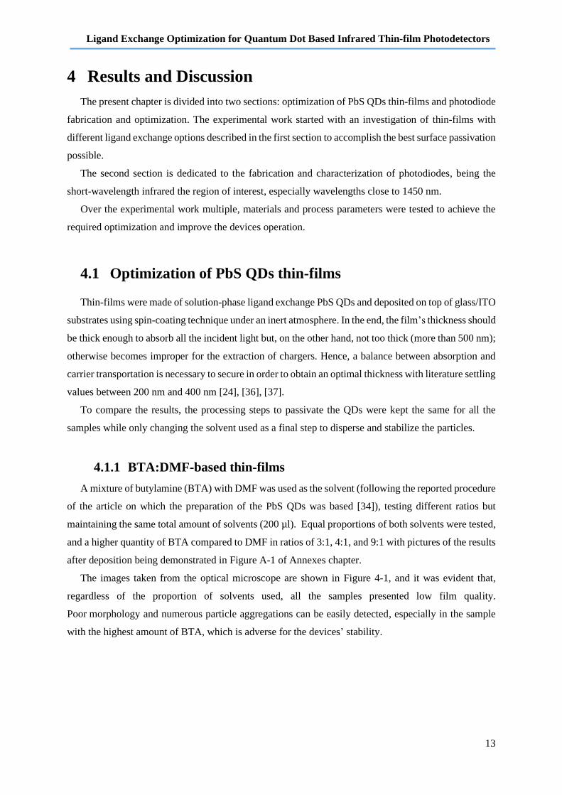
The EQE is the other figure of merit considered in order to analyze the performance of the
photodiodes. Therefore, the J-V curves with the best electronic results were chosen to be measured,
being the results shown in Figure 4-10. At first glance, it was possible to conclude that all the devices
corresponding to these curves show identical results in both graphs, being a good first indication given
the reproducibility problems mentioned above. The measurements presented in the graph of Figure
4-10 (a) were taken under constant reverse bias of -3 V showing 11% of quantum efficiency at the
wavelength of 1440 nm for the three devices tested.
The EQE voltage dependency at 1440 nm was also analysed using Figure 4-10 (b), aiming for the
lowest dependency possible. As previously referred, the increase of the rever bias leads to a higher noise
signal density (mostly because of dark current), which is why the goal is to achieve the highest EQE
value with the lowest negative bias voltage possible. By examining the results, an 11% EQE value was
reached shortly before -3 V remaining constant after that.
(a)
1100 1200 1300 1400 1500 1600 17000
5
10
15
20
EQ
E a
t -3
V (
%)
Wavelength (nm)
(b)
-5 -4 -3 -2 -1 00
5
10
15
20
EQ
E a
t 1
44
0 n
m (
%)
Bias (V)
Figure 4-10: EQE curves for the 4 QDs (BDT ligands) layers sample: (a) EQE vs. Wavelength;
(b) EQE voltage dependency graph.
Moving on to the 60 nm thick BDT ligand exchange QDs layer sample, even though the J-V
characterization (Figure 4-11 (a)) showed the same reproducibility problem, the best operational devices
had lower dark current density values but still in the magnitude of 10-5 A/cm2. The highest EQE value
at -3 V was close to the previous result (11%) for the same wavelength; however the EQE voltage
dependency (Figure 4-11 (b)) was higher and thereby worse than before due to two factors. EQE’s value
no longer starts to increase immediately after inducing negative bias voltage, and the achievement of its
highest value was only complete after -3.5 V.

Ligand Exchange Optimization for Quantum Dot Based Infrared Thin-film Photodetectors
26
(a)
(b)
-5 -4 -3 -2 -1 00
5
10
15
20
EQ
E a
t 1445 n
m (
%)
Bias (V)
1100 1200 1300 1400 1500 1600 17000
2
4
6
8
10
12
EQ
E a
t -3
V (
%)
Wavelength (nm)
Figure 4-11: Electrical characterization of the 2 QDs (BDT ligands) layers sample: (a) J-V curves;
(b) EQE voltage dependency graph and at the top right corner the EQE vs. Wavelength.
The last sample to be studied formed by the stack shown above is the sample with only one BDT
ligand exchange QDs layer. Figure 4-12 (a) presents the results for the current-voltage measurements,
demonstrating high homogeneity between the measured devices and similar performance to the
photodiodes already analyzed. On the other hand, the EQE value was for the first time greater than 11%
at the wavelength of 1440 nm, proven by Figure 4-12 (b). The same constraints of the previously
discussed sample for EQE voltage dependency were also identified for this sample.
(a)
(b)
1100 1200 1300 1400 1500 1600 17000
5
10
15
20
EQ
E a
t -3
V (
%)
Wavelength (nm)
14.5% - - - -
Figure 4-12: Electrical characterization of the 1 QDs (BDT ligands) layer sample: (a) J-V curves; (b) EQE vs. Wavelength.
The other stack employed to optimize the p-type side of the junction is illustrated by a schematic
image of the photodiode architecture in Figure 4-13. Considering the previous results collected, the
reduction of BDT ligand exchange QDs layers brought a reduction in the devices’ J-V curves’ dispersity,
as well as an increase of the EQE, and so its elimination as part of the TFPD was the step to be followed.

Ligand Exchange Optimization for Quantum Dot Based Infrared Thin-film Photodetectors
27
Hence, the p-type layer chosen to create a better p-n junction was an inorganic HTL formed by nickel
oxide.
Firstly, nickel oxide is a higher dopped material. Since the layer was prepared by a sputter deposition,
a more uniform film was attained, which may help the diode performance. Additionally, by replacing
an organic HTL (PolyTPD) with an inorganic (NiO), a more stable behavior from the devices can be
expected since typically organic materials are more sensitive to atmospheric conditions.
Comparing both stacks in relation to the fabrication process, the stack shown below is significantly
simpler than the last stack tested because it has fewer layers, therefore fewer deposition processes and
less time and material consumption. However, there is still a necessary requirement to evaluate these
materials related to the carriers’ efficient transport. PolyTPD has a bandgap from -2.3 to -5.2 eV,
ensuring a sufficient shallow CBM to block electrons, and a VBM energy suitable for alignment with
the PbS QDs treated with BDT, but despite nickel oxide also ensures efficient blocking properties, the
proper alignment with the solution-phase ligand exchange PbS QDs needs to be investigated.
Figure 4-13: Schematic image of the device architecture (stack) using nickel oxide hole transport layer, solution-phase
ligand exchange PbS QDs active layer, and titanium dioxide with niobium doping electron transport layer.
It was with enthusiasm that the analysis of the J-V measurements was done since high reproducibility
results (shown by almost completely overlapping curves in Figure 4-14) were finally accomplished,
possibly caused by the greater stability provided by the materials and stack configuration chosen.
Despite the dark current density values being close to 5 × 10⁻⁵ A/cm2, which was the magnitude of
the results for the previous stack examined, a major difference behavior between the two types of bias
is revealed, reaching current density values for the forward bias of 10-2 A/cm2. Even so, a more consistent
performance during the negative bias voltage was still missed.

Ligand Exchange Optimization for Quantum Dot Based Infrared Thin-film Photodetectors
28
Figure 4-14: J-V curves for the nickel oxide hole transport layer sample.
The measured curves in respect of EQE (Figure 4-15 (a)) indicated a difference maximum of EQE
worth mentioning between the devices tested, revealing a weak consistency of efficiency. The highest
peak corresponding to device 2 (red line) had the same efficiency as the highest EQE shown for the
previous stack samples. The only improvement was that the peak was located at 1450 nm wavelength,
which is precisely the reference value for the fabrication of these photodiodes. Both devices’ curves
illustrated in the graph of Figure 4-15 (b) only began to increase the EQE values after -2 V reaching
their maximum after -3 V exhibiting, for these reasons, an unwanted high voltage dependence.
(a)
1100 1200 1300 1400 1500 1600 17000
5
10
15
20
EQ
E a
t -3
V (
%)
Wavelength (nm)
device #1
device #2
14.3% - - - - -
11.8% - - - - -
(b)
-5 -4 -3 -2 -1 00
5
10
15
20
EQ
E a
t 1
45
0 n
m (
%)
Bias (V)
device #1
device #2
Figure 4-15: EQE curves of the nickel oxide hole transport layer sample for two devices: (a) EQE vs. Wavelength;
(b) EQE voltage dependency graph.

Ligand Exchange Optimization for Quantum Dot Based Infrared Thin-film Photodetectors
29
4.2.2 Comparison between DFP and BTA:DMF
After the extensive analysis of the different configuration stacks related to the p-type side of the
junction, the investigation was preceded by a comparison between two different types of solvents used
in the solution-phase ligand exchange process already studied in the first section of this chapter.
Whith that in mind, the last experiment performed was repeated while changing the solvent used for the
solution-phase ligand exchange layer. Instead of the 200 µl of DFP used throughout all optimization, a
mixture with a ratio of 3 to 1 corresponding to 150 µl of BDT and 50 µl of DMF was utilized since it
was the ratio that got the best results. Thereby, the stack configuration (glass/ITO/NiO/Solution-phase
LE QDs/TiO:Nb/Al) and processes were kept the same so that in the end could be possible to understand
the importance of the solvent chosen.
The J-V measurements done to the BTA:DMF sample are shown in Figure 4-16 and marked as dark
green. The measurement of device #2 was mentioned as DFP and marked with an orange color in the
same graph. Taking into consideration only the dark green curves, the uniformity between all measured
devices was again guaranteed, confirming the quality of the reproducibility that the stack offer.
When comparing the results of both samples, it becomes possible to state that there is a substantial
similarity in the devices’ behavior since, regardless of the solvent selected, the values of the current
density for the maximum positive and negative voltages were almost the same. The required constant
performance over negative bias voltage was fulfilled by the BTA:DMF sample (especially for the
devices with the lowest dark current), unlike the DFP devices and all the others studied during this
optimization.
Figure 4-16: Comparison of J-V curves for nickel oxide hole transport layer sample using BTA:DMF (dark green) or
DFP (orange).

Ligand Exchange Optimization for Quantum Dot Based Infrared Thin-film Photodetectors
30
A massive improvement in EQE under -3 V was achieved as the peak of the device corresponding to
the BTA:DMF sample was at 28.9%, being double the value reached by the best device of the DFP
sample (Figure 4-17 (a)). This discrepancy between values should be related to the efficiency of the
charge transportation due to the better carrier lifetime presented by the 3BTA:1DMF solvent upon the
optical characterization performed in the first section.
The high voltage dependence previously revealed when using DFP was not demonstrated for the
sample done with a mixture of solvents since the maximum efficiency was obtained at -2.5 V and kept
constant after that, and no longer the EQE started to rise after -2 V but rather at -1 V as shown in Figure
4-17 (b).
(a)
BTA:DMF
DFP
1100 1200 1300 1400 1500 1600 17000
5
10
15
20
25
30
35
40
EQ
E a
t -3
V (
%)
Wavelength (nm)
14.3% - - - -
28.9% - - - -
(b)
-5 -4 -3 -2 -1 00
5
10
15
20
25
30
35
40
EQ
E a
t 1
45
0 n
m (
%)
Bias (V)
BTA:DMF
DFP
Figure 4-17: Comparison of EQE curves for nickel oxide hole transport layer sample using BTA:DMF (dark green) or
DFP (orange): (a) EQE vs. Wavelength; (b) EQE voltage dependency graph.
4.2.3 Environmental conditions variations
The last sample to be discussed was chosen to be tested under different conditions, because it
presented the best electrical performance. Immediately after its electrical characterization, the sample
was subjected to ultraviolet (UV) radiation (AM1.5G conditions) for few minutes to increase the doping
concentration of the titanium dioxide layer through the light soaking phenomenon so the conductivity
of devices could potentially be enhanced [44]. The sample was then stored in a box containing oxygen
with low humidity (dry air) during a full night.
As the entire fabrication process was conducted in an N2 glove box, testing the device’s operation
under a different environment was an evaluation to be implemented, hoping that oxygen p-doping could
improve the diode performance.
To conclude, the sample was stored in an inert atmosphere (inside the glove box) for a whole day to
study whether the changes in the device performance were permanent or temporary. Thus, after each
tested situation, the device efficiency was measured, being the three curves corresponding to the three

Ligand Exchange Optimization for Quantum Dot Based Infrared Thin-film Photodetectors
31
different conditions shown in Figure 4-18. The curve obtained right after the sample’s fabrication
(instant measure) already demonstrated in Figure 4-17 (a) was also added to the graph with the highest
efficiency values reached in each condition presented in Table 4-3.
The main conclusion to be drawn from this experiment is that none of the different environments
tested improved the analyzed device’s conductivity. Starting with the first situation, the fact that there
was a 7.5% decrease in EQE after UV exposure might indicate that the junction of the stack is not
dominantly happening in the titanium dioxide interface, implying that the depletion region mainly
covers the nickel oxide region. Nevertheless, when the sample was exposed to dry air, the result was a
disaster as the highest EQE value achieved did not exceed 6%, questioning whether there was any effect
of ambient atmosphere that led to a malfunctioning device or even if there is still a junction formed.
In the end, after storing the sample in the glove box, the measurements taken proved that the different
changes performed were temporary since the efficiency was closer to the initial state.
instant measure
UV exposure
dry air exposure
inert atmosphere
1100 1200 1300 1400 1500 1600 17000
5
10
15
20
25
30
35
40
EQ
E a
t -3
V (
%)
Wavelength (nm)
Figure 4-18: EQE curves under different conditions.
Table 4-3: EQE pick values under different conditions.
Conditions EQE at 1445nm (%)
Instant measure 28.9
UV exposure 21.4
Dry air exposure 5.7
Inert atmosphere 26.2
To sum up, the stack that accomplished the best devices’ performance was developed with nickel
oxide as the hole transport layer, solution-phase ligand exchange PbS QDs as the active layer, and
titanium dioxide with niobium doping as the electron transport layer. By using a mixture of BTA with
DMF as a solvent, dark current density value close to 10-5 A/cm2 at -3 V and a total of 29% of external
quantum efficiency at 1450 nm under the same bias were revealed, concluding with success the intended
integration/optimization of the solution-phase ligand exchange QDs as part of TFPD.

Ligand Exchange Optimization for Quantum Dot Based Infrared Thin-film Photodetectors
32

Ligand Exchange Optimization for Quantum Dot Based Infrared Thin-film Photodetectors
33
5 Conclusions and Future Perspectives
The goal of the present work was to optimize the surface passivation process of quantum dots, more
specifically the ligand termination as part of infrared thin-film photodetectors. Thereby, the focus of this
research was a recent approach to implement photodetectors based on solution-phase ligand exchange
PbS QDs, which enables a simpler and lower cost process. This work is a continuation of one of the
projects conducted by the Thin-film Photodetector (TFPD) group from Imec’s Large Area Electronics
(LAE) department, which has the scope of integrate absorbing colloidal quantum dots on CMOS
imagers.
First, various methods, materials, and process parameters were explored to obtain a uniform and
smooth quantum dot thin-film with the best carrier transportation possible. During the solution’s
preparation, the primary attention was placed on the solvent by testing several types, combinations, and
amounts due to its extreme influence on the quality of the final solution.
The surface of the thin-films produced were observed through optical microscope images. Using
2,6-difluoropyridine as the solvent, a complete homogenous film without aggregations was obtained.
The morphology was also studied based on AFM measurements revealing pinhole-free results with
1.11 nm of root mean square roughness for the same thin-film. Nevertheless, films based on a mixture
of two solvents (butylamine and N,N-dimethylmethanamide) presented a slightly better optical
performance due to higher carrier lifetime values, possibly caused by the double role of the butylamine,
that not only function as a solvent but also as a ligand. A multiple passivation strategy was additionally
tried using mercaptopropionic acid in a solid-state ligand exchange approach, although without
significant differences in the optical properties results.
In the second part of the work, multi-stack quantum dot-based photodiodes were fabricated
integrating the previous study of thin-films. By maintaining the electron transport layer formed by the
titanium dioxide with niobium doping, and the active layer done by the developed ligand exchange
quantum dots process, an optimization of the p-side of the junction was carried out.
As a result and after analyzing multiple stack configurations and materials, the stack that guaranteed
the best electronic performance was composed of nickel oxide hole transport layer, solution-phase
ligand exchange PbS QDs active layer, titanium dioxide with niobium doping electron transport layer,
and top aluminum contacts. The two figures of merit evaluated were the dark current density at -3 V and
external quantum efficiency at 1450 nm wavelength, with the best device reaching values of
2.1 × 10 5 A/cm2 and 28.9%, respectively. At last, the device was measured after passing through
different environmental conditions variations. The results indicated a significant effect of the storage on
the device performance, but its initial state performance nearly recovered after the sample was stored in
inert atmosphere.

Ligand Exchange Optimization for Quantum Dot Based Infrared Thin-film Photodetectors
34
Over the course of this work there were difficult challenges to overcome mostly because of the
sensitive fabrication process of the photodiodes, along with the demanding process of the solution-phase
ligand exchange, making it harder to replicate similar performances between devices of the same stack
and even to accomplish results in every attempt. Degradation of materials, aging of solutions, processing
temperatures, humidity, thickness, concentration, and annealing temperatures of the layers are among
the parameters and process conditions responsible for a possible failure of an experiment.
A complementary characterization to the work performed would be relevant to investigate, for
instance, the unsuccessful multiple passivation strategy and to measure the average size of the particles
given its importance in the properties of the chosen active material. Therefore, X-ray Diffraction (XRD)
analysis and Transmission Electron Microscopy (TEM) are examples of techniques that could be
implemented to tackle those limitations.
In summary, a proof of concept of photodetectors based on solution-phase ligand exchange quantum
dot on glass substrates was realized. The following procedure would be to recreate the process on silicon
substrates, which requires more examination and optimization to ultimately fabricate a monolithic image
sensor for the near-infrared wavelength range.
Significant attention has been devoted to the ligand exchange strategies as a recent way to enhance
the photodetectors’ performance through the improvement of carrier mobility properties. Even so, there
is still potential needed to be fulfilled not only in the mentioned topic but also in new device architectures
and transport layer materials, so that the colloidal quantum dots infrared sensors technology meets the
desired commercialization and mass production point.

Ligand Exchange Optimization for Quantum Dot Based Infrared Thin-film Photodetectors
35
Bibliography
[1] Z. Győri et al., “Laser-induced fluorescence measurements on CdSe quantum dots”, Process.
Appl. Ceram., vol. 4, no. 1, pp. 33–38, 2010.
[2] A. I. Ekimov and A. A. Onushchenko, “Quantum Size Effect in Three-Dimensional Microscopic
Semiconductor Crystals”, Pis’ma Zh. Eksp. Teor. Fiz, vol. 34, no. 6, pp. 363–366, 1981.
[3] X. Li et al., “Bright colloidal quantum dot light-emitting diodes enabled by efficient
chlorination”, Nat. Photonics, vol. 12, no. 3, pp. 159–164, 2018, doi: 10.1038/s41566-018-
0105-8.
[4] H. Shen et al., “Visible quantum dot light-emitting diodes with simultaneous high brightness and
efficiency”, Nat. Photonics, vol. 13, no. 3, pp. 192–197, 2019, doi: 10.1038/s41566-019-0364-z.
[5] S. Pradhan et al., “High-efficiency colloidal quantum dot infrared light-emitting diodes via
engineering at the supra-nanocrystalline level”, Nat. Nanotechnol., vol. 14, no. 1, pp. 72–79,
2019, doi: 10.1038/s41565-018-0312-y.
[6] L. Qian, Y. Zheng, J. Xue, and P. H. Holloway, “Stable and efficient quantum-dot light-emitting
diodes based on solution-processed multilayer structures”, Nat. Photonics, vol. 5, no. 9, pp. 543–
548, 2011, doi: 10.1038/NPHOTON.2011.171.
[7] X. Tang, M. M. Ackerman, M. Chen, and P. Guyot-sionnest, “Dual-band infrared imaging using
stacked colloidal quantum dot photodiodes”, Nat. Photonics, vol. 13, no. 4, pp. 277–282, 2019,
doi: 10.1038/s41566-019-0362-1.
[8] G. Konstantatos et al., “Ultrasensitive solution-cast quantum dot photodetectors”, Nature,
vol. 442, no. 7, pp. 180–183, 2006, doi: 10.1038/nature04855.
[9] S. A. Mcdonald et al., “Solution-processed PbS quantum dot infrared photodetectors and
photovoltaics”, Nat. Mater., vol. 4, no. 2, pp. 138–142, 2005, doi: 10.1038/nmat1299.
[10] R. Saran and R. J. Curry, “Lead sulphide nanocrystal photodetector technologies”,
Nat. Photonics, vol. 10, no. 2, pp. 81–92, 2016, doi: 10.1038/nphoton.2015.280.
[11] C. Wang, B. L. Wehrenberg, C. Y. Woo, and P. Guyot-sionnest, “Light Emission and
Amplification in Charged CdSe Quantum Dots”, J. Phys. Chem. B, vol. 108, no. 26, pp. 9027–
9031, 2004, doi: 10.1021/jp0489830.
[12] S. Hoogland, V. Sukhovatkin, I. Howard, S. Cauchi, L. Levina, and E. H. Sargent, “A solution-
processed 1.53 μm quantum dot laser with temperature-invariant emission wavelength”,
Opt. Express, vol. 14, no. 8, pp. 3273–3281, 2006, doi: 10.1364/OE.14.003273.
[13] J. Xu et al., “2D matrix engineering for homogeneous quantum dot coupling in photovoltaic
solids”, Nat. Nanotechnol., vol. 13, no. 6, pp. 456–462, Jun. 2018, doi: 10.1038/s41565-018-
0117-z.
[14] A. Swarnkar et al., “Quantum dot–induced phase stabilization of α-CsPbI3 perovskite for high-
efficiency photovoltaics”, Science, vol. 354, no. 6308, pp. 92–95, 2016,

Ligand Exchange Optimization for Quantum Dot Based Infrared Thin-film Photodetectors
36
doi: 10.1126/science.aag2700.
[15] J. Van Embden, A. S. R. Chesman, and J. J. Jasieniak, “The heat-up synthesis of colloidal
nanocrystals”, Chem. Mater., vol. 27, no. 7, pp. 2246–2285, 2015, doi: 10.1021/cm5028964.
[16] S. G. Kwon and T. Hyeon, “Formation mechanisms of uniform nanocrystals via hot-injection
and heat-up methods”, Small, vol. 7, no. 19, pp. 2685–2702, 2011, doi: 10.1002/smll.201002022.
[17] H. Li, C. Wang, Z. Peng, and X. Fu, “A Review on the Synthesis Methods of CdSeS-Based
Nanostructures”, J. Nanomater., vol. 2015, no. 5, pp. 1–16, 2015, doi: 10.1155/2015/519385.
[18] J. Park, J. Joo, G. K. Soon, Y. Jang, and T. Hyeon, “Synthesis of monodisperse spherical
nanocrystals”, Angew. Chemie - Int. Ed., vol. 46, no. 25, pp. 4630–4660, 2007,
doi: 10.1002/anie.200603148.
[19] G. H. Carey, A. L. Abdelhady, Z. Ning, S. M. Thon, O. M. Bakr, and E. H. Sargent, “Colloidal
Quantum Dot Solar Cells”, Chemical Reviews, vol. 115, no. 23. pp. 12732–12763, 2015,
doi: 10.1021/acs.chemrev.5b00063.
[20] G. K. Soon et al., “Kinetics of monodisperse iron oxide nanocrystal formation by ‘heating-up’
process”, J. Am. Chem. Soc., vol. 129, no. 41, pp. 12571–12584, 2007, doi: 10.1021/ja074633q.
[21] A. P. Alivisatos, “Perspectives on the Physical Chemistry of Semiconductor Nanocrystals”,
J. Phys. Chem., vol. 100, no. 31, pp. 13226–13239, 1996, doi: 10.1021/jp9535506.
[22] P. E. Malinowski et al., “Thin-film quantum dot photodiode for monolithic infrared image
sensors”, Sensors (Switzerland), vol. 17, no. 12, p. 2867, 2017, doi: 10.3390/s17122867.
[23] J. P. Clifford, G. Konstantatos, K. W. Johnston, S. Hoogland, L. Levina, and E. H. Sargent, “Fast,
sensitive and spectrally tuneable colloidal-quantum-dot photodetectors”, vol. 4, no. 1, pp. 40–
44, 2009, doi: 10.1038/NNANO.2008.313.
[24] M. Liu et al., “Hybrid organic-inorganic inks flatten the energy landscape in colloidal
quantum dot solids”, Nat. Mater., vol. 16, no. 2, pp. 258–263, 2017, doi: 10.1038/nmat4800.
[25] P. R. Brown et al., “Energy level modification in lead sulfide quantum dot thin films through
ligand exchange”, ACS Nano, vol. 8, no. 6, pp. 5863–5872, 2014, doi: 10.1021/nn500897c.
[26] J. Tang and E. H. Sargent, “Infrared colloidal quantum dots for photovoltaics: Fundamentals and
recent progress”, Adv. Mater., vol. 23, no. 1, pp. 12–29, 2011, doi: 10.1002/adma.201001491.
[27] Q. Lin et al., “Phase-Transfer Ligand Exchange of Lead Chalcogenide Quantum Dots for Direct
Deposition of Thick, Highly Conductive Films”, J. Am. Chem. Soc., vol. 139, no. 19, pp. 6644–
6653, 2017, doi: 10.1021/jacs.7b01327.
[28] H. R. You, J. Y. Park, D. H. Lee, Y. Kim, and J. Choi, “Recent research progress in surface
ligand exchange of PbS quantum dots for solar cell application”, Applied Sciences, vol. 10, no.3,
p. 975, 2020, doi: 10.3390/app10030975.
[29] G. H. Carey, K. W. Chou, B. Yan, A. R. Kirmani, A. Amassian, and E. H. Sargent, “Materials
processing strategies for colloidal quantum dot solar cells: advances, present-day limitations, and
pathways to improvement”, MRS Commun., vol. 3, no. 2, pp. 83–90, 2013,

Ligand Exchange Optimization for Quantum Dot Based Infrared Thin-film Photodetectors
37
doi: 10.1557/mrc.2013.17.
[30] J. Z. Fan et al., “Mixed Lead Halide Passivation of Quantum Dots”, Adv. Mater., vol. 31, no. 48,
2019, doi: 10.1002/adma.201904304.
[31] A. Nag, M. V Kovalenko, J. Lee, W. Liu, B. Spokoyny, and D. V Talapin, “Metal-free Inorganic
Ligands for Colloidal Nanocrystals”, J. Am. Chem. Soc., vol. 133, no. 27, pp. 10612–10620,
2011, doi: 10.1021/ja2029415.
[32] M. J. Choi et al., “Cascade surface modification of colloidal quantum dot inks enables efficient
bulk homojunction photovoltaics”, Nat. Commun., vol. 11, no. 1, p. 103, 2020,
doi: 10.1038/s41467-019-13437-2.
[33] G. I. Koleilat et al., “Efficient , Stable Infrared Photovoltaics Quantum Dots”, ACS Nano, vol. 2,
no. 5, pp. 833–840, 2008, doi: 10.1021/nn800093v.
[34] Y. Kim et al., “A Facet-Specific Quantum Dot Passivation Strategy for Colloid Management and
Efficient Infrared Photovoltaics”, Adv. Mater., vol. 31, no. 17, 2019,
doi: 10.1002/adma.201805580.
[35] I. M. Hossain et al., “Scalable Processing of Low Temperature TiO Nanoparticles for High
Efficiency Perovskite Solar Cells”, ACS Appl. Energy Mater., vol. 2, no. 1, pp. 47–58, 2019,
doi: 10.1021/acsaem.8b01567.
[36] X. Yang et al., “Enhanced Passivation and Carrier Collection in Ink-Processed PbS Quantum
Dots Solar Cells via Supplementary Ligand Strategy”, ACS Appl. Mater. Interfaces, vol. 12,
no. 37, pp. 42217–42225, 2020, doi: 10.1021/acsami.0c08135.
[37] J. Z. Fan et al., “Micron Thick Colloidal Quantum Dot Solids”, Nano Lett., vol. 20, no. 7,
pp. 5284–5291, 2020, doi: 10.1021/acs.nanolett.0c01614.
[38] M. Gu et al., “Stable PbS quantum dot ink for efficient solar cells by solution-phase ligand
engineering”, J. Mater. Chem. A, vol. 7, no. 26, pp. 15951–15959, 2019,
doi: 10.1039/c9ta02393c.
[39] B. S. Hinds, L. Levina, E. J. D. Klem, G. Konstantatos, V. Sukhovatkin, and E. H. Sargent,
“Smooth-Morphology Ultrasensitive Solution-Processed Photodetectors”, Adv. Mater., vol. 20,
no. 23, pp. 4398–4402, 2008, doi: 10.1002/adma.200800452.
[40] B. N. Pal, I. Robel, A. Mohite, R. Laocharoensuk, D. J. Werder, and V. I. Klimov, “High-
Sensitivity p-n junction photodiodes based on Pbs nanocrystal quantum dots”, Adv. Funct.
Mater., vol. 22, no. 8, pp. 1741–1748, 2012, doi: 10.1002/adfm.201102532.
[41] E. J. D. Klem, C. Gregory, D. Temple, and J. Lewis, “PbS colloidal quantum dot photodiodes
for low-cost SWIR sensing”, Infrared Technol., vol. 9451, pp. 17–21, 2015,
doi: 10.1117/12.2178532.
[42] E. Georgitzikis et al., “Optimization of Charge Carrier Extraction in Colloidal Quantum Dots
Short-Wave Infrared Photodiodes through Optical Engineering”, Adv. Funct. Mater., vol. 28,
no. 42, 2018, doi: 10.1002/adfm.201804502.

Ligand Exchange Optimization for Quantum Dot Based Infrared Thin-film Photodetectors
38
[43] J. Hu, Y. Shi, Z. Zhang, R. Zhi, S. Yang, and B. Zou, “Recent progress of infrared photodetectors
based on lead chalcogenide colloidal quantum dots”, Chinese Phys. B, vol. 28, no. 2, 2019,
doi: 10.1088/1674-1056/28/2/020701.
[44] J. Choi et al., “Activated Electron-Transport Layers for Infrared Quantum Dot Optoelectronics”,
Adv. Mater., vol. 30, no. 12, 2018, doi: 10.1002/adma.201801720.
Ligand Exchange Optimization for Quantum Dot Based Infrared Thin-film Photodetectors
39
Annexes
A. Pictures of the BTA:DMF-based thin-films
Figure A-1: Thin-films fabricated based on BTA:DMF solvent.

Ligand Exchange Optimization for Quantum Dot Based Infrared Thin-film Photodetectors
40
B. Pictures of the BTA:DFP and DFP-based thin-films
Figure B-2: Thin-films fabricated based on DFP and BTA:DFP solvent.

Ligand Exchange Optimization for Quantum Dot Based Infrared Thin-film Photodetectors
41
C. Comparation of final solutions with and without
mercaptopropionic acid
Figure C-3: Final solution with the addition of mercaptopropionic acid.
Figure C-4: Standard final solution before deposition (without mercaptopropionic acid).

Ligand Exchange Optimization for Quantum Dot Based Infrared Thin-film Photodetectors
42
D. Synthesis of quantum dots with the addition of lead chloride
Figure D-5: Aggregation of particles formed during the synthesis.