
Lg Lac m1600
31
DETACHABLE FRONT PANEL CAR CD RECEIVER SERVICE MANUAL CAUTION BEFORE SERVICING THE UNIT, READ THE “SAFETY PRECAUTIONS” IN THIS MANUAL. MODEL:LAC-M1600R SERVICE MANUAL MODEL:LAC-M1600R
-
Upload
mircea-alex -
Category
Documents
-
view
48 -
download
4
description
LG service car audio
Transcript of Lg Lac m1600

DETACHABLE FRONTPANEL CAR CD RECEIVERSERVICE MANUALCAUTIONBEFORE SERVICING THE UNIT, READ THE “SAFETY PRECAUTIONS”IN THIS MANUAL.
MODEL:LAC-M1600R
SE
RV
ICE
MA
NU
AL
MO
DE
L:L
AC
-M1600R

- 1-1 -
[CONTENTS]
SECTION 1.GENERAL• SERVICING PRECAUTIONS . . . . . . . . . . . . . . . . . . . . . . . . . . . . . . . . . . . . . . . . . . . . . . . 1-2
• ESD PRECAUTIONS . . . . . . . . . . . . . . . . . . . . . . . . . . . . . . . . . . . . . . . . . . . . . . . . . . . . . 1-3
• SPECIFICATIONS . . . . . . . . . . . . . . . . . . . . . . . . . . . . . . . . . . . . . . . . . . . . . . . . . . . . . . . .1-4
SECTION 2. ELECTRICAL• ELECTRICAL TROUBLESHOOTING GUIDE . . . . . . . . . . . . . . . . . . . . . . . . . . . . . . . . . . . . 2-1
• WAVEFORMS OF MAJOR CHECK POINT . . . . . . . . . . . . . . . . . . . . . . . . . . . . . . . . . . . . . 2-6
• INTERNAL BLOCK DIAGRAM of ICs . . . . . . . . . . . . . . . . . . . . . . . . . . . . . . . . . . . . . . . . . 2-7
• BLOCK DIAGRAM . . . . . . . . . . . . . . . . . . . . . . . . . . . . . . . . . . . . . . . . . . . . . . . . . . . . . . . 2-17
• SCHEMATIC DIAGRAMS . . . . . . . . . . . . . . . . . . . . . . . . . . . . . . . . . . . . . . . . . . . . . . . . . 2-19
• PRINTED CIRCUIT DIARGAMS . . . . . . . . . . . . . . . . . . . . . . . . . . . . . . . . . . . . . . . . . . . . 2-27
SECTION 3. EXPLODED VIEWS• CABINET AND MAIN FRAME SECTION . . . . . . . . . . . . . . . . . . . . . . . . . . . . . . . . . . . . . . . 3-1
• MECHANISM (PICK-UP) . . . . . . . . . . . . . . . . . . . . . . . . . . . . . . . . . . . . . . . . . . . . . . . . . . . 3-3
SECTION 4. REPLACEMENT PARTS LIST . . . . . . . . . . . . . . . . . . . . . . . . . . .4-1
- 1-2 -
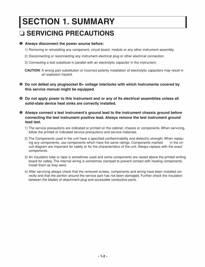
SECTION 1. SUMMARY SERVICING PRECAUTIONS❶ Always disconnect the power source before:
1) Removing or reinstalling any component, circuit board, module or any other instrument assembly.
2) Disconnecting or reconnecting any instrument electrical plug or other electrical connection.
3) Connecting a test substitute in parallel with an electrolytic capacitor in the instrument.
CAUTION: A wrong part substitution or incorrect polarity installation of electrolytic capacitors may result inan explosion hazard.
❷ Do not defeat any plug/socket B+ voltage interlocks with which instruments covered bythis service manual might be equipped.
❹ Do not apply power to this instrument and or any of its electrical assemblies unless allsolid-state device heat sinks are correctly installed.
❸ Always connect a test instrument’s ground lead to the instrument chassis ground beforeconnecting the test instrument positive lead. Always remove the test instrument groundlead last.
1) The service precautions are indicated or printed on the cabinet, chassis or components. When servicing,follow the printed or indicated service precautions and service materials.
2) The Components used in the unit have a specified conflammability and dielectric strength. When replac-ing any components, use components which have the same ratings. Components marked in the cir-cuit diagram are important for safety or for the characteristics of the unit. Always replace with the exactcomponents.
3) An insulation tube or tape is sometimes used and some components are raised above the printed writingboard for safety. The internal wiring is sometimes clamped to prevent contact with heating components.Install them as they were.
4) After servicing always check that the removed screws, components and wiring have been installed cor-rectly and that the portion around the service part has not been damaged. Further check the insulationbetween the blades of attachment plug and accessible conductive parts.

- 1-3 -
ESD PRECAUTIONSElectrostatically Sensitive Devices (ESD)Some semiconductor (solid state) devices can be damaged easily by static electricity. Such componentscommonly are called Electrostatically Sensitive Devices (ESD). Examples of typical ESD devices are integratedcircuits and some field-effect transistors and semiconductor chip components. The following techniques shouldbe used to help reduce the incidence of component damage caused by static electricity.
1. Immediately before handling any semiconductor component or semiconductor-equipped assembly, drain offany electrostatic charge on your body by touching a known earth ground. Alternatively, obtain and wear acommercially available discharging wrist strap device, which should be removed for potential shock reasonsprior to applying power to the unit under test.
2. After removing an electrical assembly equipped with ESD devices, place the assembly on a conductive sur-face such as aluminum foil, to prevent electrostatic charge buildup or exposure of the assembly.
3. Use only a grounded-tip soldering iron to solder or unsolder ESD devices.
4. Use only an anti-static solder removal device. Some solder removal devices not classified as "anti-static" cangenerate electrical charges sufficient to damage ESD devices.
5. Do not use freon-propelled chemicals. These can generate electrical charges sufficient to damage ESDdevices.
6. Do not remove a replacement ESD device from its protective package until immediately before you areready to install it. (Most replacement ESD devices are packaged with leads electrically shorted together byconductive foam, aluminum foil or comparable conductive materials).
7. Immediately before removing the protective material from the leads of a replacement ESD device, touch theprotective material to the chassis or circuit assembly into which the device will by installed.
CAUTION : BE SURE NO POWER IS APPLIED TO THE CHASSIS OR CIRCUIT, AND OBSERVE ALLOTHER SAFETY PRECAUTIONS.
8. Minimize bodily motions when handing unpackaged replacement ESD devices. (Otherwise harmless motionsuch as the brushing together of your clothes fabric or the lifting of your foot from a carpeted floor can gen-erate static electricity sufficient to damage an ESD device).
CAUTION. GRAPHIC SYMBOLS
THE LIGHTNING FLASH WITH APROWHEAD SYMBOL. WITHIN AN EQUILATERAL TRIANGLE,IS INTENDED TO ALERT THE SERVICE PERSONNEL TO THE PRESENCE OF UNINSULATED“DANGEROUS VOLTAGE” THAT MAY BE OF SUFFICIENT MAGNITUDE TO CONSTITUTE ARISK OF ELECTRIC SHOCK.
THE EXCLAMATION POINT WITHIN AN EQUILATERAL TRIANGLE IS INTENDED TO ALERTTHE SERVICE PERSONNEL TO THE PRESENCE OF IMPORTANT SAFETY INFORMATION INSERVICE LITERATURE.
- 1-4 -
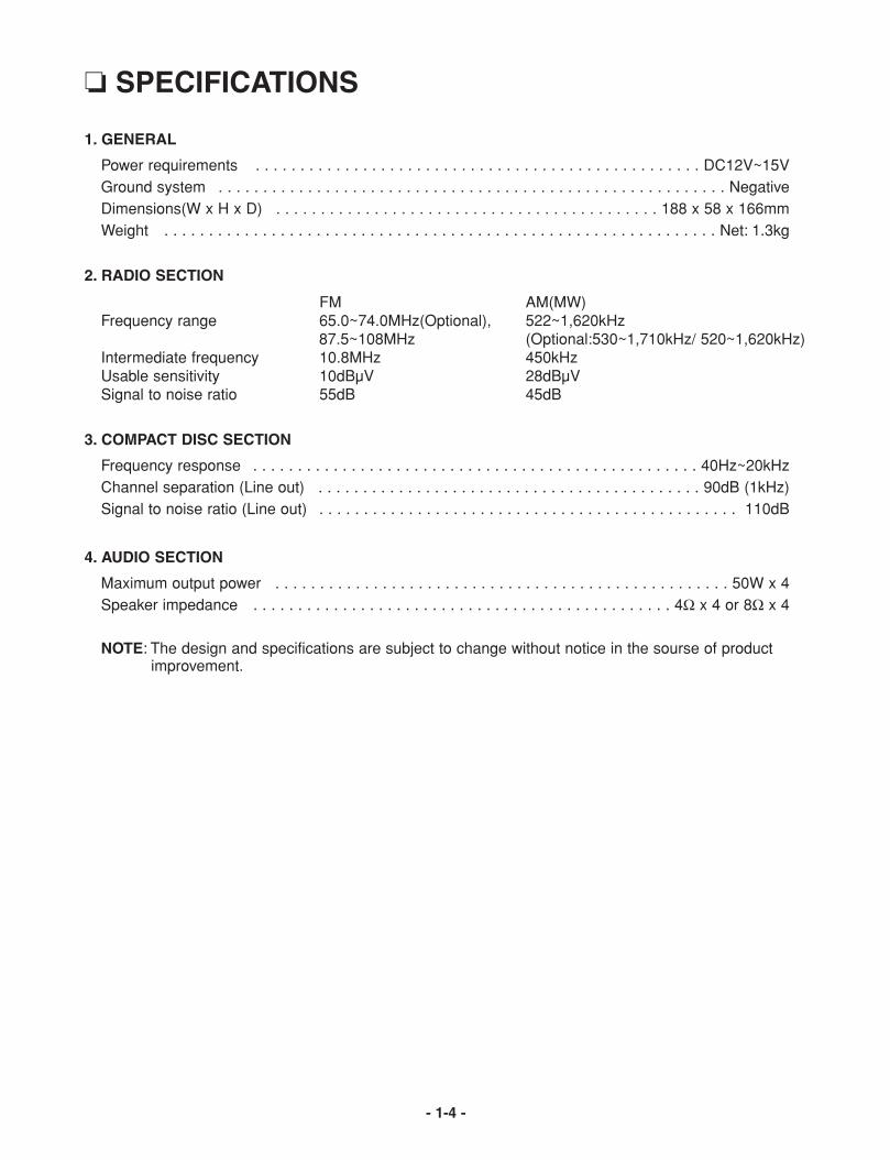
SPECIFICATIONS
1. GENERAL
Power requirements . . . . . . . . . . . . . . . . . . . . . . . . . . . . . . . . . . . . . . . . . . . . . . . . . . DC12V~15VGround system . . . . . . . . . . . . . . . . . . . . . . . . . . . . . . . . . . . . . . . . . . . . . . . . . . . . . . . . . NegativeDimensions(W x H x D) . . . . . . . . . . . . . . . . . . . . . . . . . . . . . . . . . . . . . . . . . . . 188 x 58 x 166mmWeight . . . . . . . . . . . . . . . . . . . . . . . . . . . . . . . . . . . . . . . . . . . . . . . . . . . . . . . . . . . . . . Net: 1.3kg
2. RADIO SECTION
FM AM(MW)Frequency range 65.0~74.0MHz(Optional), 522~1,620kHz
87.5~108MHz (Optional:530~1,710kHz/ 520~1,620kHz)Intermediate frequency 10.8MHz 450kHzUsable sensitivity 10dBµV 28dBµVSignal to noise ratio 55dB 45dB
3. COMPACT DISC SECTION
Frequency response . . . . . . . . . . . . . . . . . . . . . . . . . . . . . . . . . . . . . . . . . . . . . . . . . . 40Hz~20kHzChannel separation (Line out) . . . . . . . . . . . . . . . . . . . . . . . . . . . . . . . . . . . . . . . . . . . 90dB (1kHz)Signal to noise ratio (Line out) . . . . . . . . . . . . . . . . . . . . . . . . . . . . . . . . . . . . . . . . . . . . . . . 110dB
4. AUDIO SECTION
Maximum output power . . . . . . . . . . . . . . . . . . . . . . . . . . . . . . . . . . . . . . . . . . . . . . . . . . . 50W x 4Speaker impedance . . . . . . . . . . . . . . . . . . . . . . . . . . . . . . . . . . . . . . . . . . . . . . . 4Ω x 4 or 8Ω x 4
NOTE: The design and specifications are subject to change without notice in the sourse of productimprovement.
- 2-1 -
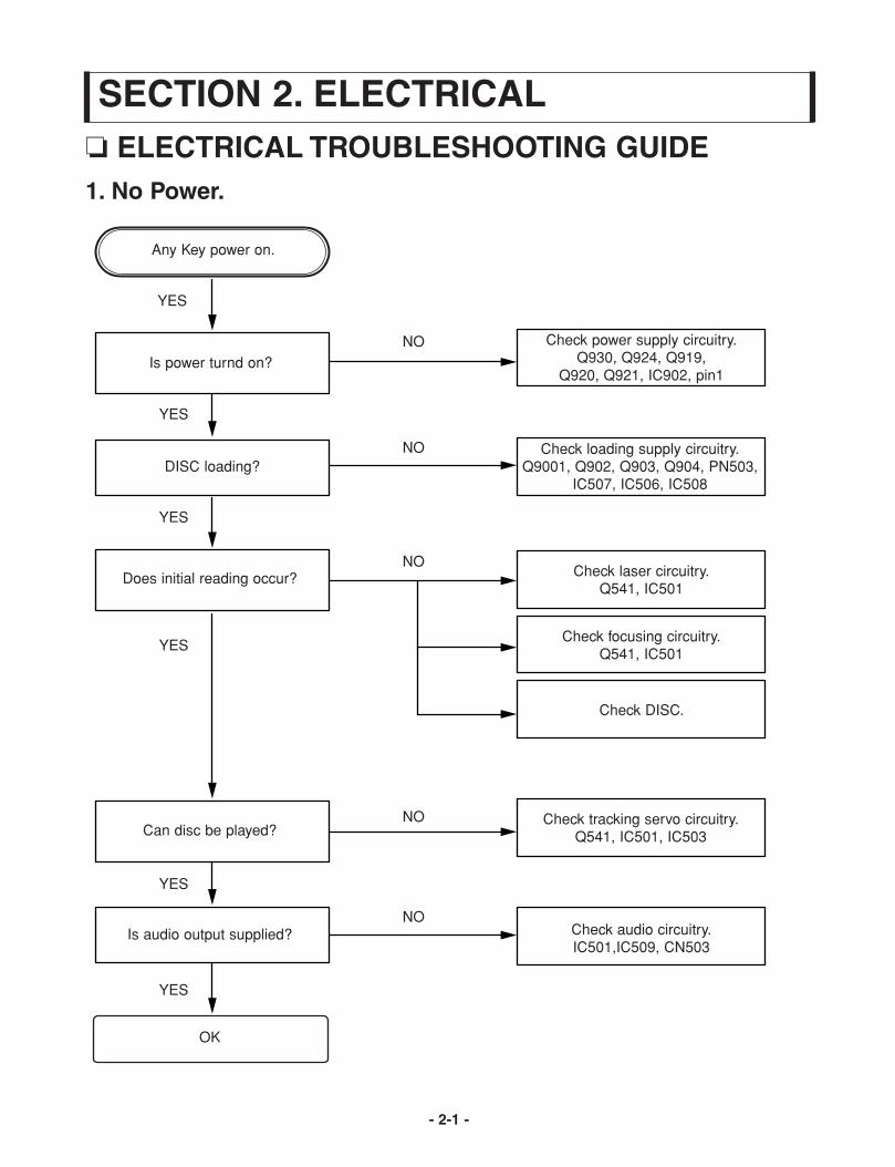
SECTION 2. ELECTRICAL ELECTRICAL TROUBLESHOOTING GUIDE1. No Power.
Any Key power on.
YES
YES
YES
YES
YES
YES
NO
NO
NO
NO
NO
Is power turnd on?
DISC loading?
Does initial reading occur?
Can disc be played?
Is audio output supplied?
OK
Check audio circuitry.IC501,IC509, CN503
Check tracking servo circuitry.Q541, IC501, IC503
Check DISC.
Check focusing circuitry.Q541, IC501
Check laser circuitry.Q541, IC501
Check loading supply circuitry.Q9001, Q902, Q903, Q904, PN503,
IC507, IC506, IC508
Check power supply circuitry.Q930, Q924, Q919,
Q920, Q921, IC902, pin1
- 2-2 -
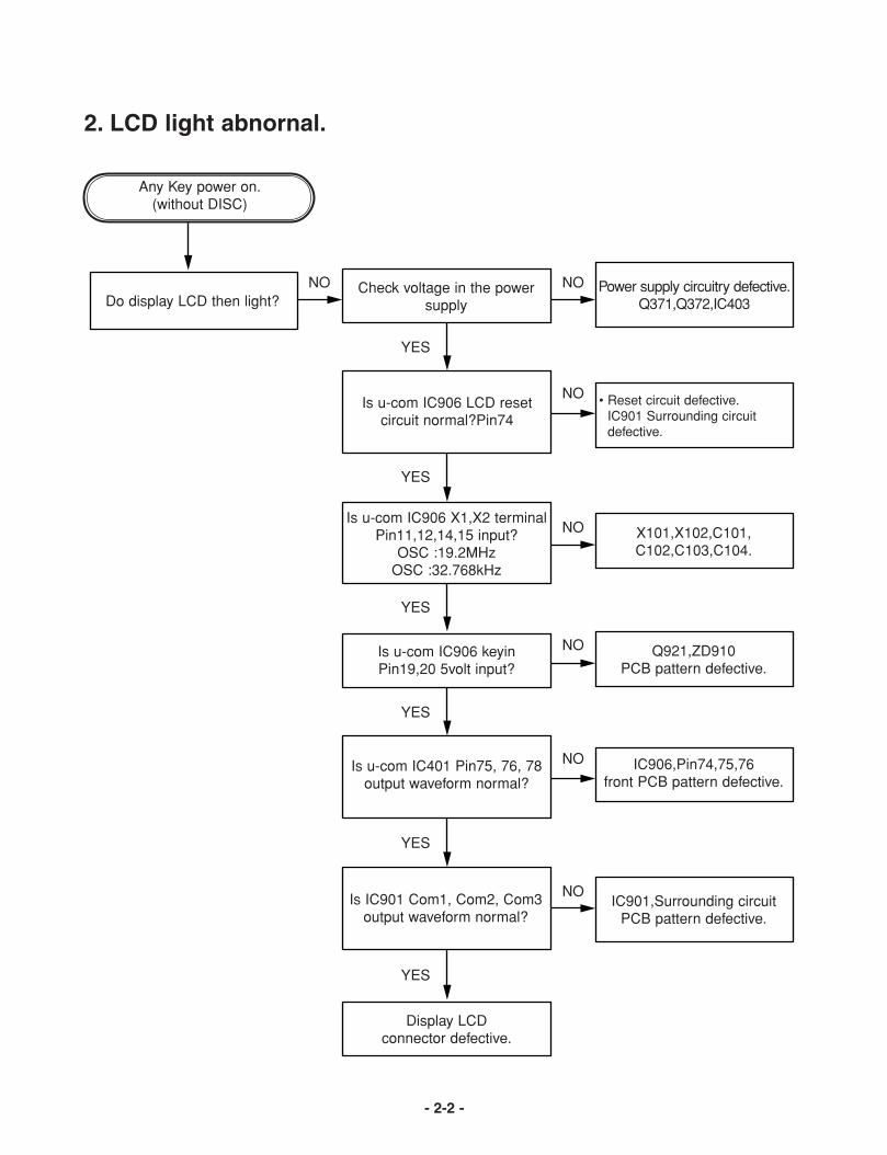
2. LCD light abnornal.
YES
YES
YES
YES
YES
YES
NO NO
NO
NO
NO
NO
NO
Any Key power on.(without DISC)
Do display LCD then light?Check voltage in the power
supplyPower supply circuitry defective.
Q371,Q372,IC403
• Reset circuit defective.IC901 Surrounding circuitdefective.
X101,X102,C101,C102,C103,C104.
Q921,ZD910PCB pattern defective.
IC906,Pin74,75,76front PCB pattern defective.
IC901,Surrounding circuitPCB pattern defective.
Display LCD connector defective.
Is IC901 Com1, Com2, Com3output waveform normal?
Is u-com IC401 Pin75, 76, 78output waveform normal?
Is u-com IC906 LCD resetcircuit normal?Pin74
Is u-com IC906 keyinPin19,20 5volt input?
Is u-com IC906 X1,X2 terminalPin11,12,14,15 input?
OSC :19.2MHzOSC :32.768kHz

- 2-3 -
3. Initial reading is not carried out.
YES
YES
YES
YES
YES
YES
YES
YES
YES
YES
YES
YES
YES (with disc)
NO NO
NO
NO
NO
NO
NO
NO
NO
NO
NO
Slide motor moves(With disc)
Spindle motor turnsWAVEFORM #1
Does RF waveformappear? IC501 Pin49
WAVEFORM #2
Check the Voltage change ofCN503 Pin12 (6.4~6.8V)
Check the Voltage IC501Pin23 (1.4V~1.8V)
Check the Data transmissionfrom CN503 (16, 17, 18) to CD
DSP WAVEFORM #5
Check the Data transmissionfrom CN503 Pin21 to MICOM
WAVEFORM #5
Check the TRVP Voltage
IC501 Pin23
Check the change ofSL +, SL - Voltage
IC503 Pin13,14
Does FA+ waveform appear atIC501 Pin23?
WAVEFORM #3
Laser light check A ?
focus coil drive wareform.
TRACKING ERROR wareform
Defective contact CN501Defective PICK-UP
Defective IC503
Defective IC501
Defective connector CN503Defective IC503
Defective connectorCN503 Defective
MICOM
Defective IC501
Defective connector CN503
Does TE waveform appear atIC501 Pin24?
WAVEFORM #4
Defective IC501Defective PICK-UP
Is rotation normal?
Is there no dropout of RF signal?

- 2-4 -
When laser does not light.A
Is “2.4V~3.4V” applied to pin42 of IC501?
( ➀ 3.4V ➁ 2.4V)
Did pickup return to innermost circular?
Does it stop at inner pickcircular after shift?
Is defect output from LMTSW applied to Pin7 of
PN503?
Is data transferred fromMICOM IC ?
Does voltage appear atIC503 Pin 13, 14?
Defective MICOM or CN503.
Defective IC501.
Defective slide motor and/orconnector. (CN502)
Defective LMT SW and/orconnector. (CN502,CN503)
Defective MICOM.
Defective IC501Is power supplied to laser Q541?(Q541 collector: about 1.8V)
OV
YES
YES
YESYES
YES
YES
NO
NO
NO
NO
NO
NO
OPEN CLOSE
- 2-5 -
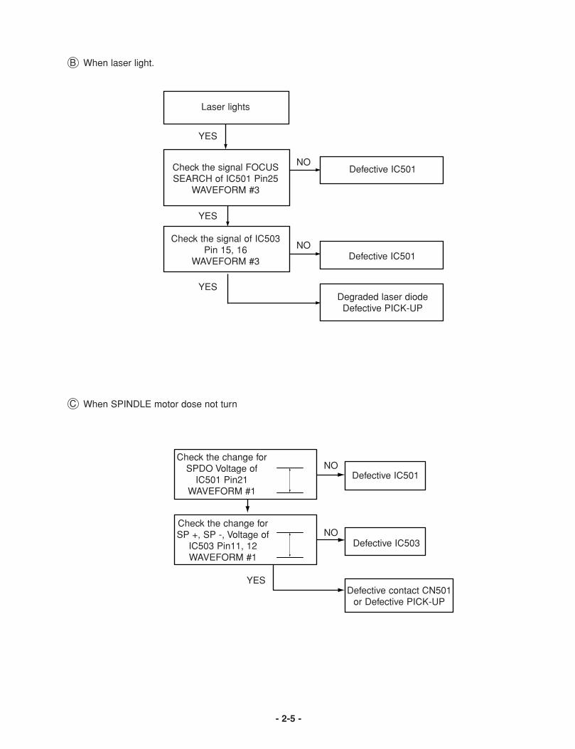
When laser light.B
When SPINDLE motor dose not turnC
NO
NO
NO
NO
YES
YES
YES
YES
Laser lights
Check the signal FOCUSSEARCH of IC501 Pin25
WAVEFORM #3
Check the signal of IC503Pin 15, 16
WAVEFORM #3 Defective IC501
Defective IC501
Degraded laser diodeDefective PICK-UP
Defective IC501
Defective IC503
Defective contact CN501or Defective PICK-UP
Check the change forSP +, SP -, Voltage of
IC503 Pin11, 12WAVEFORM #1
Check the change forSPDO Voltage of
IC501 Pin21WAVEFORM #1

- 2-6 -
WAVEFORMS OF MAJOR CHECK POINT
#1. SPINDLE DRIVE AND MOTOR WAVEFORMIC501(21), IC504(12) during TOC reading
#2. RF WAVEFORMIC501(45), IC501(49) during TOC reading
#3. FOCUS DRIVE AND MOTOR WAVEFORMIC501(25), IC503(15)
• When focus search failed or there is no disc on tray
#4. TRACK DRIVE AND MOTOR WAVEFORMIC504(24), IC503(17) during TOC reading
• There is disc on tray and focus search success
- 2-7 -
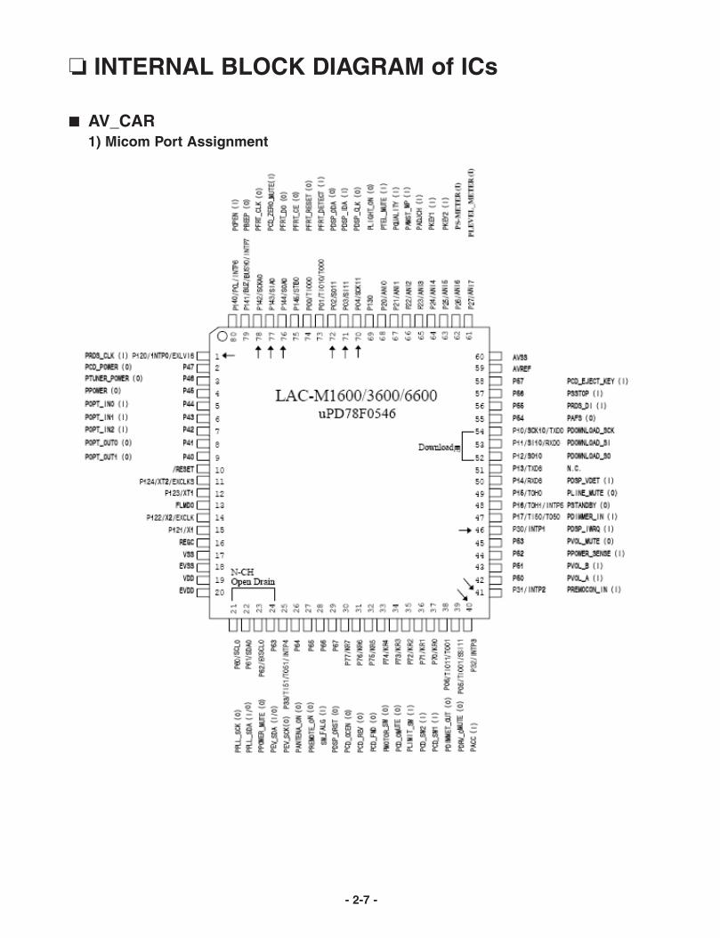
INTERNAL BLOCK DIAGRAM of ICs
AV_CAR1) Micom Port Assignment

- 2-8 -
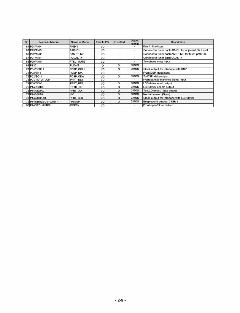
2) Pin Descriptions
- 2-9 -

- 2-10 -
BD3805F1) BLOCK DIAGRAM

- 2-11 -
MN6627933CN(DSP)1) Connection Diagram

- 2-12 -
TA8275HQ1) Block Diagram
- 2-13 -
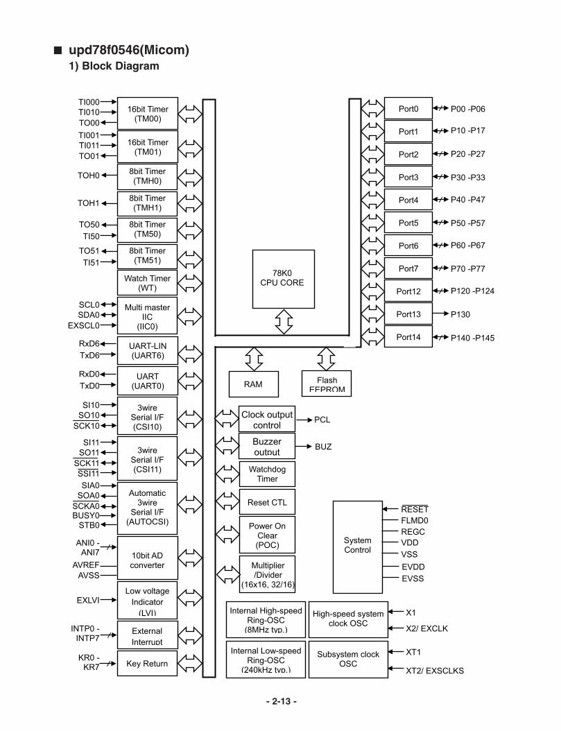
upd78f0546(Micom)1) Block Diagram

- 2-14 -
2) Pin lay out
- 2-15 -
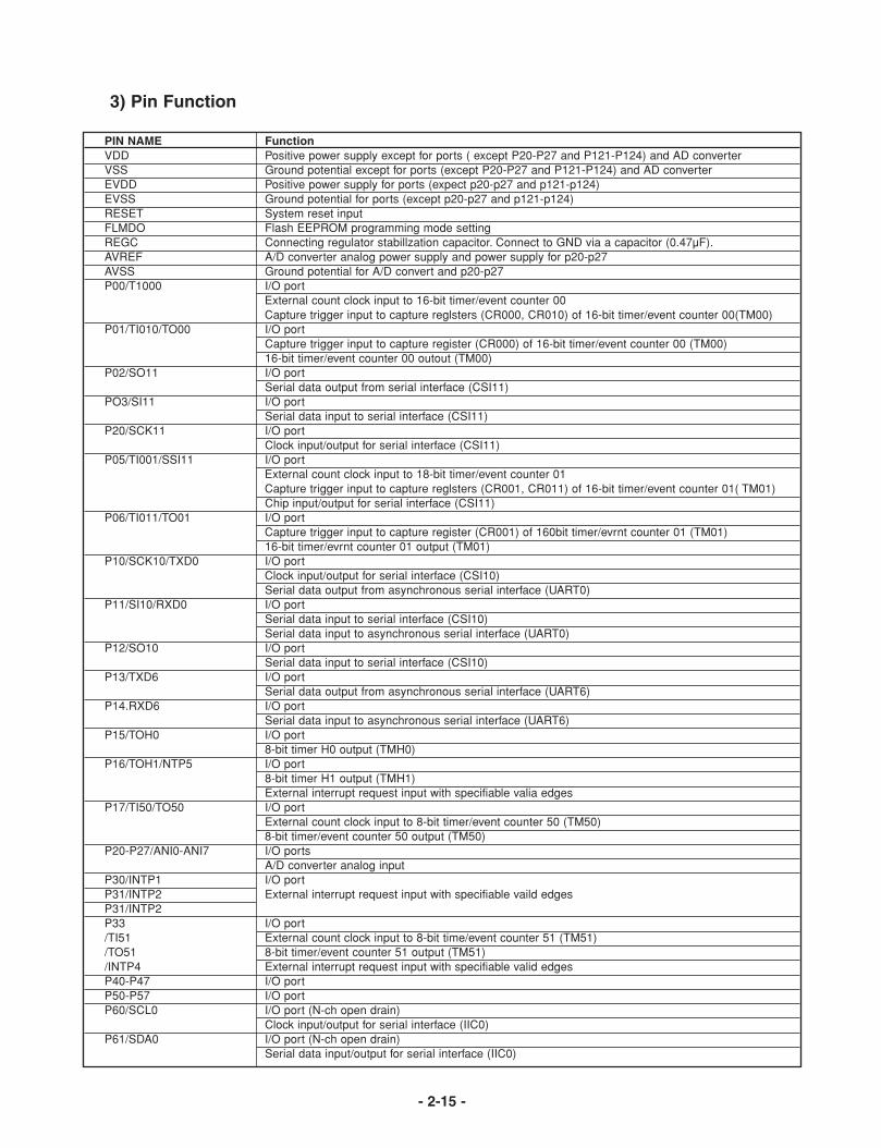
3) Pin Function
PIN NAME FunctionVDD Positive power supply except for ports ( except P20-P27 and P121-P124) and AD converterVSS Ground potential except for ports (except P20-P27 and P121-P124) and AD converterEVDD Positive power supply for ports (expect p20-p27 and p121-p124) EVSS Ground potential for ports (except p20-p27 and p121-p124)RESET System reset inputFLMDO Flash EEPROM programming mode settingREGC Connecting regulator stabillzation capacitor. Connect to GND via a capacitor (0.47µF).AVREF A/D converter analog power supply and power supply for p20-p27AVSS Ground potential for A/D convert and p20-p27P00/T1000 I/O port
External count clock input to 16-bit timer/event counter 00Capture trigger input to capture reglsters (CR000, CR010) of 16-bit timer/event counter 00(TM00)
P01/TI010/TO00 I/O portCapture trigger input to capture register (CR000) of 16-bit timer/event counter 00 (TM00)16-bit timer/event counter 00 outout (TM00)
P02/SO11 I/O portSerial data output from serial interface (CSI11)
PO3/SI11 I/O portSerial data input to serial interface (CSI11)
P20/SCK11 I/O portClock input/output for serial interface (CSI11)
P05/TI001/SSI11 I/O portExternal count clock input to 18-bit timer/event counter 01 Capture trigger input to capture reglsters (CR001, CR011) of 16-bit timer/event counter 01( TM01)Chip input/output for serial interface (CSI11)
P06/TI011/TO01 I/O portCapture trigger input to capture register (CR001) of 160bit timer/evrnt counter 01 (TM01)16-bit timer/evrnt counter 01 output (TM01)
P10/SCK10/TXD0 I/O portClock input/output for serial interface (CSI10)Serial data output from asynchronous serial interface (UART0)
P11/SI10/RXD0 I/O portSerial data input to serial interface (CSI10)Serial data input to asynchronous serial interface (UART0)
P12/SO10 I/O portSerial data input to serial interface (CSI10)
P13/TXD6 I/O portSerial data output from asynchronous serial interface (UART6)
P14.RXD6 I/O portSerial data input to asynchronous serial interface (UART6)
P15/TOH0 I/O port8-bit timer H0 output (TMH0)
P16/TOH1/NTP5 I/O port8-bit timer H1 output (TMH1)External interrupt request input with specifiable valia edges
P17/TI50/TO50 I/O portExternal count clock input to 8-bit timer/event counter 50 (TM50)8-bit timer/event counter 50 output (TM50)
P20-P27/ANI0-ANI7 I/O portsA/D converter analog input
P30/INTP1 I/O portP31/INTP2 External interrupt request input with specifiable vaild edgesP31/INTP2P33 I/O port/TI51 External count clock input to 8-bit time/event counter 51 (TM51)/TO51 8-bit timer/event counter 51 output (TM51)/INTP4 External interrupt request input with specifiable valid edgesP40-P47 I/O portP50-P57 I/O portP60/SCL0 I/O port (N-ch open drain)
Clock input/output for serial interface (IIC0)P61/SDA0 I/O port (N-ch open drain)
Serial data input/output for serial interface (IIC0)

- 2-16 -
PIN NAME FunctionP62/EXSCL0 I/O port (N-ch open drain)
External clock input for serial interface (IIC0)P63 I/O port (N-ch open drain)P64-P67 I/O portsP70-P77 I/O ports/KR0-KR7 Key interrupt inputP120 I/O port/INTP0 External interrupt request input with specifiable vaild edges/EXLVI Reference voltsge input for low voltage indicatorP121 I/O port (An external oscillation circuit is not used)/X1 Connecting resonator for main system clock oscillationP122 I/O port (An external oscillation circuit is not used)/X2 Connecting resonator for main system clock oscillation/EXCLK External clock input for main system clockP123 I/O port (An external oscillation circuit is not used) XT1 connecting resonator for subsystem clock oscillationP123 I/O port (An external oscillation circuit is not used)XT1 Connecting resonator for subsystem clock oscillation P124 I/O port (An external oscillation circuit is not used)/XT2 Connecting resonator for subsystem clock oscillation/EXCLKS External clock input for subsystem clockP130 Output portP140 I/O port/PCL Clock output/INTP6 External interrupt request input with specifiable vaild edgeP141 I/O port/PCL Clock output/INTP7 External interrupt requwst input with specifiable vaild edge/BUSY0 Busy signal input for serial interface (AUTOCSI)P142 I/O port/SCKA0 Clock input/output for serial interface (AUTOCSI)P143 I/O port/SIA0 Serial data input to serial interface P144 I/O port/SOA0 Serial data output from serial interface (AUTOCSI)P145 I/O port/STB0 Strobe signal input to serial interface (AUTOCSI)
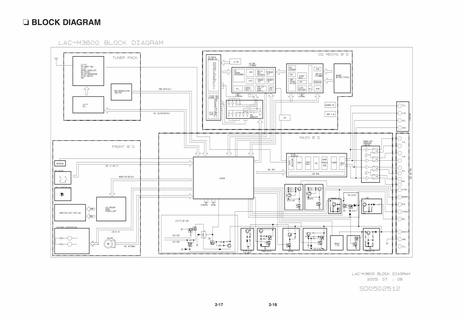
BLOCK DIAGRAM
2-17 2-18
2-19 2-20
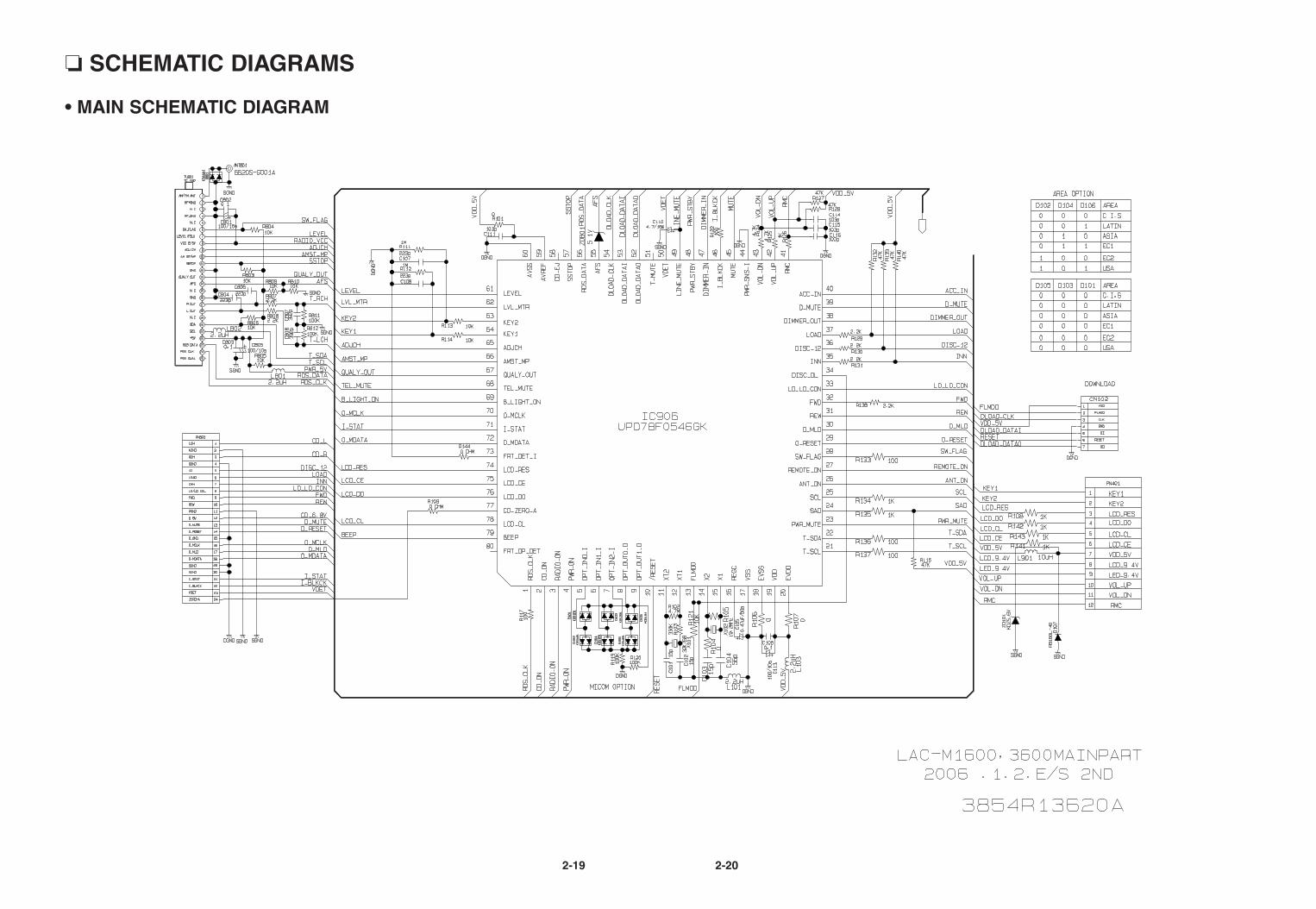
SCHEMATIC DIAGRAMS
• MAIN SCHEMATIC DIAGRAM

2-21 2-22
• MAIN-2 SCHEMATIC DIAGRAM

2-23 2-24
• FRONT SCHEMATIC DIAGRAM

2-25 2-26
• CD SCHEMATIC DIAGRAM
2-27 2-28
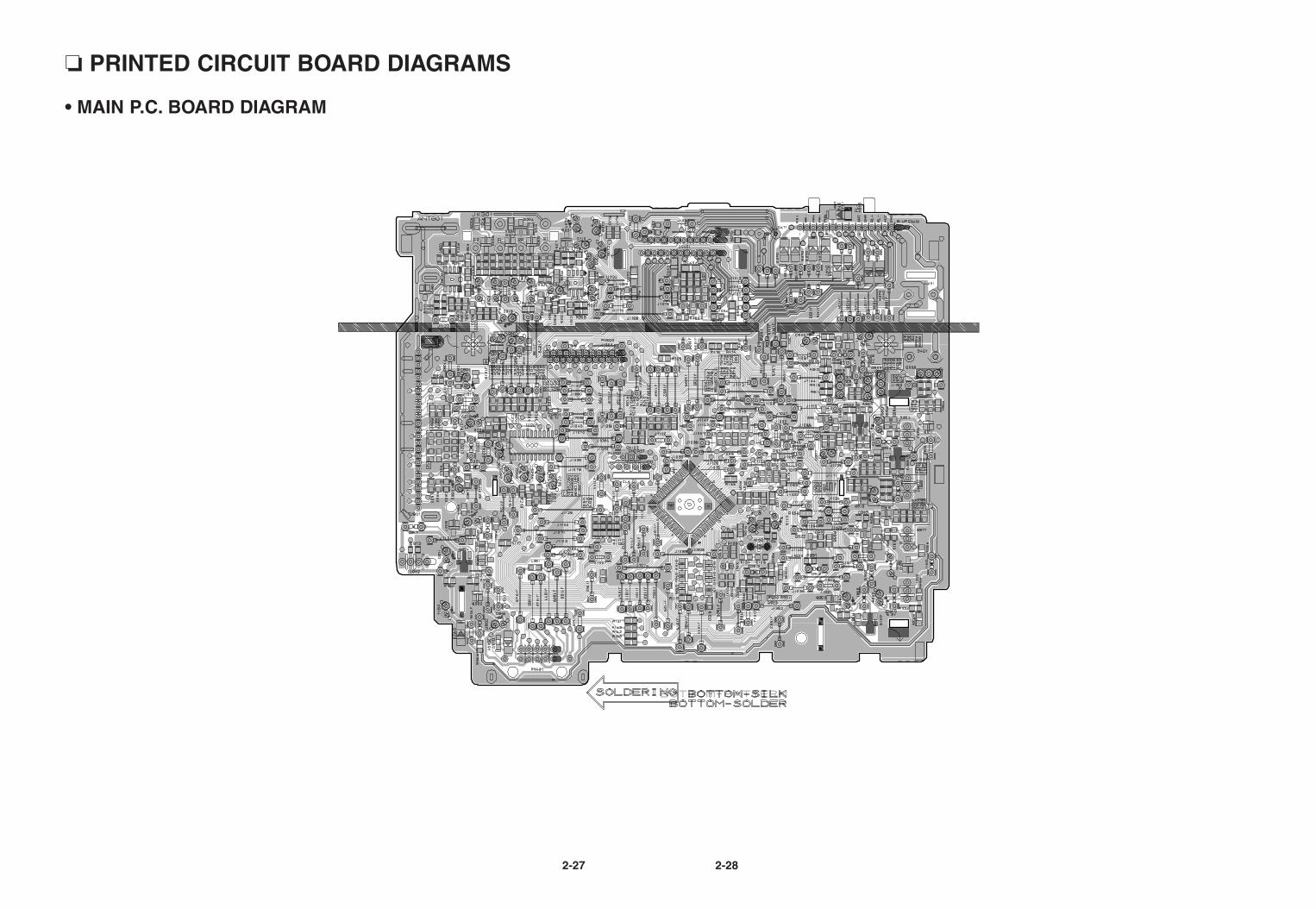
PRINTED CIRCUIT BOARD DIAGRAMS
• MAIN P.C. BOARD DIAGRAM

2-29 2-30
• FRONT/TRIM P.C. BOARD DIAGRAM • LED P.C. BOARD

2-31 2-32
• CD P.C. BOARD
3-1 3-2
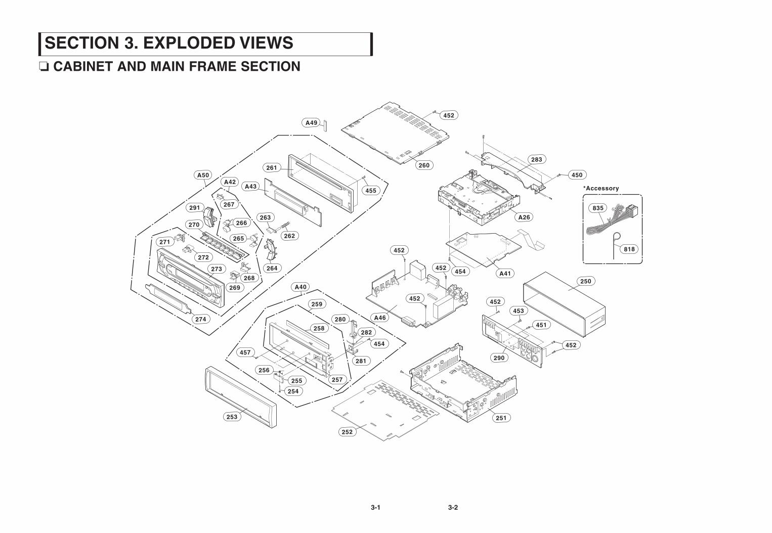
452
283
450
250
451
453452
452
452
A40
259
258280
454
281
282
257
452
A41
A26
260
455A43
261
454
262
264
269
268
263
265
267
266
272
273
274
271
270
291
A50A42
A46
452
290
251
252
253
254
255
256
457
A49
835
818
*Accessory
SECTION 3. EXPLODED VIEWS CABINET AND MAIN FRAME SECTION
3-3 3-4
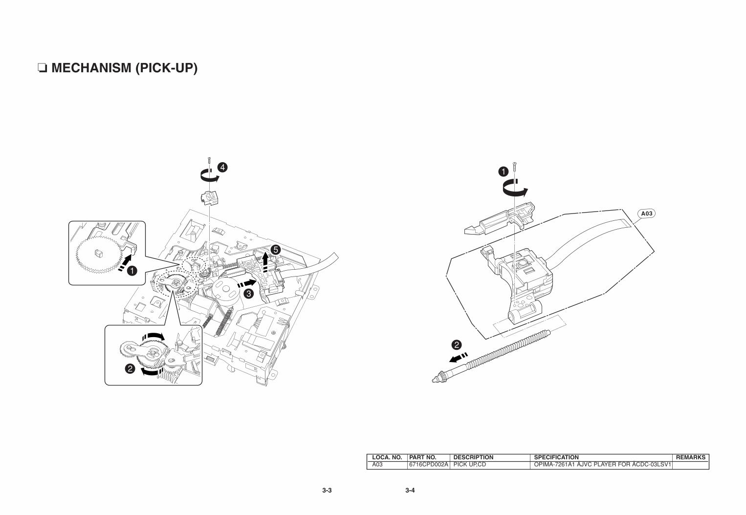
2
3
4
5
1
1
2
A03
MECHANISM (PICK-UP)
LOCA. NO. PART NO. DESCRIPTION SPECIFICATION REMARKSA03 6716CPD002A PICK UP,CD OPIMA-7261A1 ÄJVC PLAYER FOR ÄCDC-03LSV1