Lectures 15-16 Graphene and - Lancaster University€¦ · carbon nanotubes Graphene is atomically...
25
Lectures 15-16 Graphene and carbon nanotubes Graphene is atomically thin crystal of carbon which is stronger than steel but flexible, is transparent for light, and conducts electricity (gapless semiconductor).
Transcript of Lectures 15-16 Graphene and - Lancaster University€¦ · carbon nanotubes Graphene is atomically...

Lectures 15-16
Graphene and
carbon nanotubes
Graphene is atomically thin crystal of carbon which is stronger than steel but flexible, is transparent for light, and conducts electricity (gapless semiconductor).

D.I.Y.Graphene
Geim & Novoselov(Manchester) 2004

Graphene from a nanopensilKim (Columbia Univ) 2005Kim (Columbia Univ) 2005

Ultra-thin graphitic films mechanically exfoliated from bulk graphite
Novoselov & Geim (Manchester)Science 306, 666 (2004)
Geim & Novoselov - Nature Materials 6, 183 (2007)Geim & MacDonald Physics Today 60 35 41 (2007)
, ( )
Geim & MacDonald, Physics Today 60, 35-41 (2007)Geim & Kim, Scientific American 90-97 (April 2008)
10 nm

hybridisation forms strong directed bonds2sp
Carbon has 4 electrons in the outer s-p shell
hybridisation forms strong directed bonds which determine a honeycomb lattice structure.p
C
- bonds
*Strong hybridised bonds
make graphene mechanically strong.It takes 48,000 kN·m·kg−1
2sp empty
?- conduction properties
(compare to best steel's 154 kN·m·kg−1). Also, it is chemically resilient.
strong covalent bonds
full

hexagonal Bravais lattice unit cell – can be u t ce ca bechosen differently
2 full
221121ananR nn
6 x 1/3 sites
2 full sites
6 x 1/3 sites

hybridisation forms strong directed bonds2sp
Carbon has 4 electrons in the outer s-p shell
hybridisation forms strong directed bonds which determine a honeycomb lattice structure.p
C
- bonds
)(zp orbitals determine conduction properties of graphite
eV3~0
)(p orbitals determine conduction properties of graphite
*
eV10~pz-bands

Bragg scattering conditions
GNGNG
RGi
Reciprocal lattice
MRG nn 221
221121GNGNG NN 121 nnRGieaGaG 1
1112||;
G
21
unitcell
aGaG
S
2222
111
2||;
||;
2GunitcellS
GaG 222 ||;
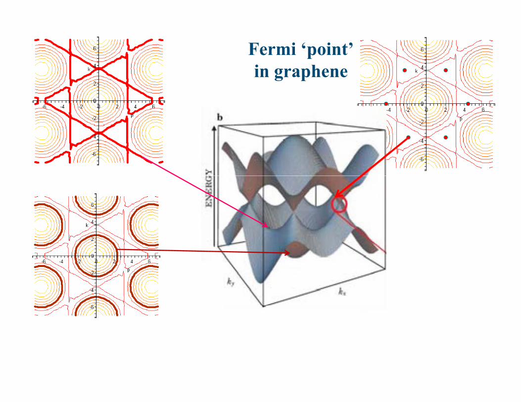
Hexagonal Bravais lattice determines a hexagonal reciprocal lattice, with
a 42
1G
aaaGG
34
2/32||||
221

Reciprocal lattice
GNGNG
)()( kGk
Hexagonal
221121GNGNG NN )()(
21kGk NN
Hexagonal reciprocal lattice corresponding to
the hexagonalG the hexagonal
Bravais lattice2G
1st Brilloun zone
1G
1G
Fermi ‘point’in graphenein graphene
FEk )(
G Valley G y
'G

Graphene (monolayer of graphite)Graphene (monolayer of graphite) is an atomically thin zero-gap
two-dimensional semiconductor with linear dispersion ofwith linear dispersion of
conduction and valence band electrons.
22cond ppvvp yx ppvvp
pElectronic dispersion in the vicinity of the corner of
xpyp
22val ppvvp
the Brillouin zone: the same in both valleys.
yx ppvvp

high-energy photon ħω~100-1000eV
Simultaneous detection of the energy, E and
ti l θ fħω 100-1000eV propagation angle θ of photo-electrons enablesonemEp cos2|| one
to restorecompletely
the band structure.EAp
mEp )(
cos2
||
||
A l l d h i i (ARPES)
the band structure.
work function
Angle-resolved photo-emission spectroscopy (ARPES) of heavily doped graphene synthesized on silicon carbide
A. Bostwick et al – Nature Physics, 3, 36 (2007)

DoS
Graphene: gapless semiconductorDoS
h l l t
gatecarriers Vn
holes electronsWallace, Phys. Rev. 71, 622 (1947)
Graphene-based field-effect transistor: GraFET GraFET
Geim and Novoselov, Nature Mat. 6, 183 (2007)

Graphene-based pixels
When embedded in polymers, graphene reinforces them, remains
grapheneg p ,conducting and, since it’s thin, it is
highly transparent.Thus it is an ideal material to makeThus, it is an ideal material to make
flexible liquid crystal screens
or to be used in conducting coating.Blake (Graphene Industries Ltd), et al
Nano Lett. 8, 1704, (2008)

Graphene: state of the art in applicaitons
G exfoliated from bulk graphite into
G grown on copper andtransferred into various media
G sublimated on inch-size SiC is used g p
suspensions is used to enhance mechanical
properties of light-weight
transferred into various media is used for flexible optoelectronics,
LCD displays, touch screens.
for manufacturing THz circuits. IBM & HRL (USA)IBM & HRL (USA)
materials (for aerospace and medical implants ).
(Samsung)


Carbon nanotubes
Iijima 1991Smalley 1993
STM images of carbon nanotubesT.W. Odom, J.-L. Huang, P.Kim, C.Lieber, Nature 391 (1998)

Nanotubes growth

Nanotube typesNanotube types
armchair (n,n) metallic
i ( 0) i d tzig-zag (n,0) semiconductor
chiral (n m) small gapchiral (n,m) small-gap with n-m=3 semiconductors

LyyLyi
)()0(/21
Metallic nanotubes (n,n)
Mp
e LyiL
2
~ /21
perimeter, 2πr
ML
py
22yx
cond ppv 2
222
LMhpv x
condn1n
yx pp
p
3210n0nF
xpyp
22Mh
,....3,2,1,0nxp
22yx
val ppv 22
LMhpv x
valn

1M
Metallic nanotubes (m,m’) with m=m’ truly 1D conductors
d it
0M
p
density of states
11M 1M|| xpvxp
v
DoS1
0M
1M|| xp
Yao et al (TUDelft)1999

Semicondutor-type nanotubes(different n and m)
D di h th b h t i ll d i tDepending on how the carbon sheet is rolled into a nanotube, the resulting nanotube may have a gap in
the electron spectrum. A gap in the nanotube spectrum is determined by its radius r, which offers p y ,
a direct root towards engineering semiconductor wires with a prescribed band gap, for use in
electronic and optoelectronic devices.
v
gap
rv
xpgap
tunnelling currentT.W. Odom, J.-L. Huang, P. Kim, C. Lieber, Nature 391 (1998)

Potential applications of carbon nanotubes:
In surface tunnelling microscopy – used as a tip.
Make excellent tips for field-effect electron guns for plasma. displays (SONY).
equi-potential linesequ pote t a es

Northwest Doctoral Training Centre
in Nanoscience
Initial training designed to demonstrate the breadth and potential of nanoscience, before focusing on one specific area of the subject.nanoscience, before focusing on one specific area of the subject.
Research and training in fundamental nanoscience, practical nano-engineering, and nanotechnology in medicine.
Interdisciplinary PhD projects which span from development and studies (exp and th) of fundamental properties of new materials and structures to making devices for applications in electronics and medicine. g pp
Development of skills in nanofabrication, low-temperature physics, materials science and data storage, synthetic chemistry, cell &tissue biology biophysics nanophotonics and materials science – this will be biology, biophysics, nanophotonics and materials science – this will be your choice!