Lecture C Semiconductor circuit elements and dependent sources.
26
Lecture C Semiconductor circuit elements and dependent sources
-
Upload
randolf-cannon -
Category
Documents
-
view
222 -
download
2
Transcript of Lecture C Semiconductor circuit elements and dependent sources.
Lecture C
Semiconductor circuit elements and dependent sources

Semiconductor devices and active circuit elements
• Examples:
• Metal Oxide Semiconductor Field Effect Transistors (MOSFETs)
• Bipolar Junction Transistors (BJTs)
• Operational amplifiers (op-amps)
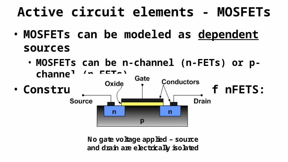
Active circuit elements - MOSFETs
• MOSFETs can be modeled as dependent sources• MOSFETs can be n-channel (n-FETs) or p-channel (p-FETs)
• Construction and operation of nFETS:
No gate voltage applied – source and drain are electrically isolated

MOSFET operation – continued• Application of a voltage difference between the gate and
source allows current to flow from the drain to the source.
Positive gate voltage applied – “channel” opens between source and drain, allowing flow of current
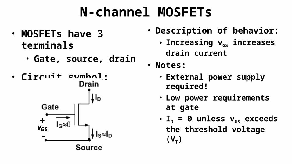
N-channel MOSFETs• MOSFETs have 3 terminals
• Gate, source, drain
• Circuit symbol:
• Description of behavior:• Increasing vGS increases
drain current• Notes:
• External power supply required!
• Low power requirements at gate
• ID = 0 unless vGS exceeds the threshold voltage (VT)
+
-vGS
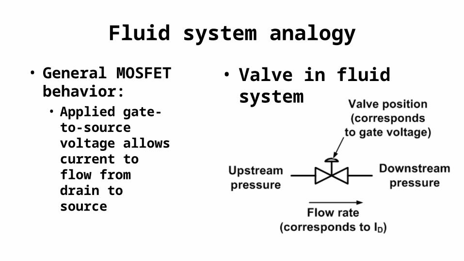
Fluid system analogy
• General MOSFET behavior:• Applied gate-to-
source voltage allows current to flow from drain to source
• Valve in fluid system
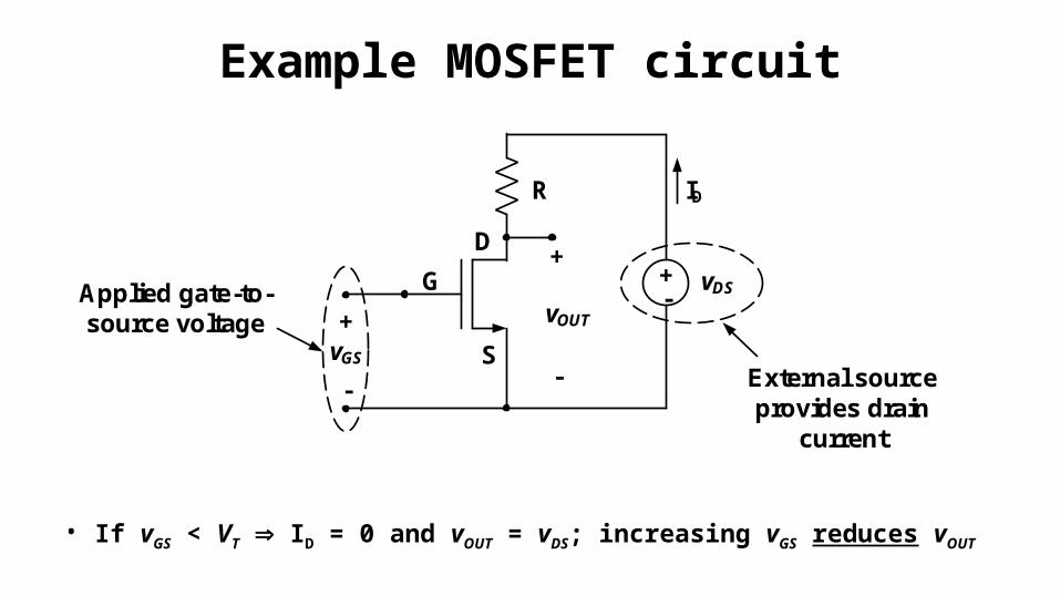
Example MOSFET circuit
• If vGS < VT ID = 0 and vOUT = vDS; increasing vGS reduces vOUT
G
S
D+-
vDS
ID
External source provides drain
current
R
+
-
vGS
Applied gate-to-source voltage
+
-
vOUT

MOSFETs as switches• If the gate voltage of the MOSFET toggles between two
values, the MOSFET can behave as a switch:

MOSFETs as dependent sources
• Approximate i-v curves:• Simple saturation-region
MOSFET model:
• Notes:• VT is the threshold voltage;
ID = 0 if vGS < VT
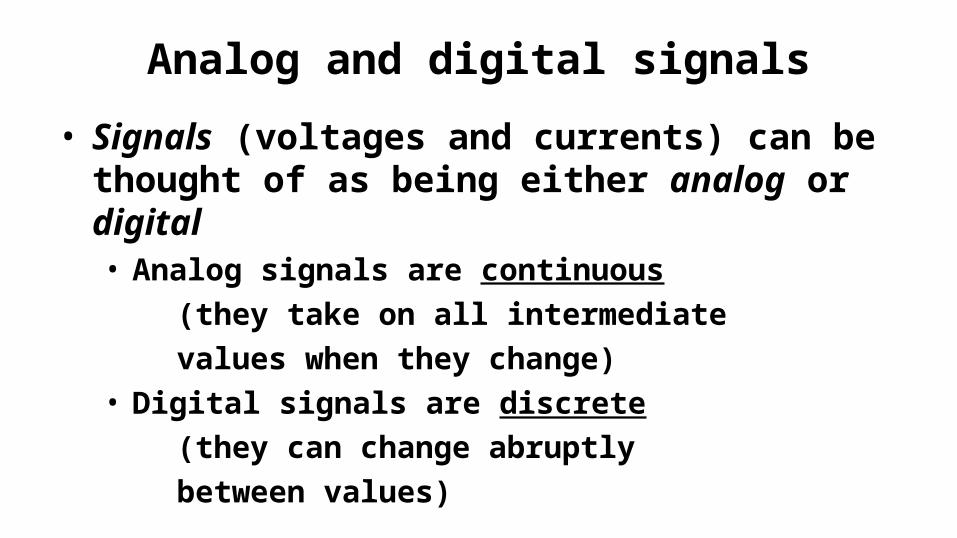
Analog and digital signals
• Signals (voltages and currents) can be thought of as being either analog or digital• Analog signals are continuous (they take on all intermediate values when they change)• Digital signals are discrete (they can change abruptly between values)
• Reminder: annotate previous slide to show analog, digital signal.
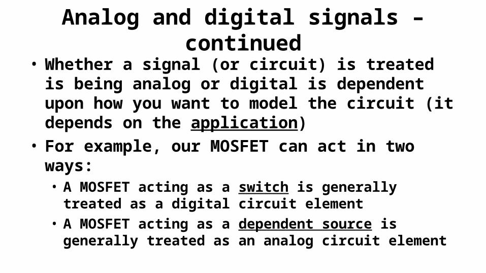
Analog and digital signals – continued• Whether a signal (or circuit) is treated is being
analog or digital is dependent upon how you want to model the circuit (it depends on the application)
• For example, our MOSFET can act in two ways:• A MOSFET acting as a switch is generally treated as a
digital circuit element• A MOSFET acting as a dependent source is generally
treated as an analog circuit element

p-channel MOSFETs
• Operation of p-channel MOSFETs (p-FETs) is “similar” to n-FETs, EXCEPT:
• Negative gate voltage applied, and current direction reversed
• Operation is “inverted” from the n-FET operation
• Demos:– Show MOSFETS– Show variation in source current with gate voltage. (Emphasize that external
power supply is required)
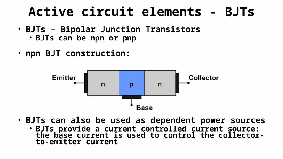
Active circuit elements - BJTs• BJTs – Bipolar Junction Transistors
• BJTs can be npn or pnp
• npn BJT construction:
• BJTs can also be used as dependent power sources• BJTs provide a current controlled current source: the base
current is used to control the collector-to-emitter current
• Discussion:– Probably counter-productive to try to do a
detailed discussion of BJT operation.– What (basically) happens is that an applied base
current allows a much larger current to flow from the collector to the emitter
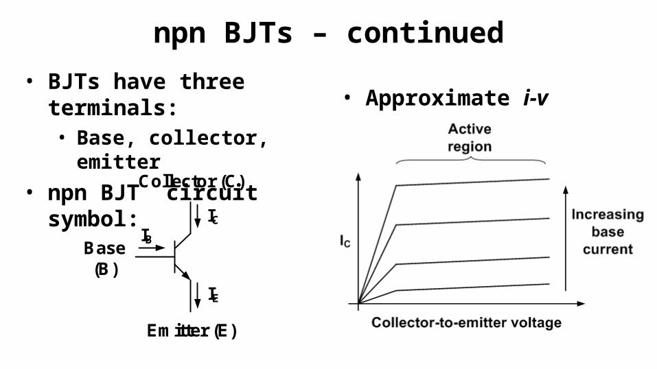
npn BJTs – continued• BJTs have three terminals:
• Base, collector, emitter• npn BJT circuit symbol:
• Approximate i-v curves:
Emitter (E)
Base(B)
Collector (C)
IC
IE
IB
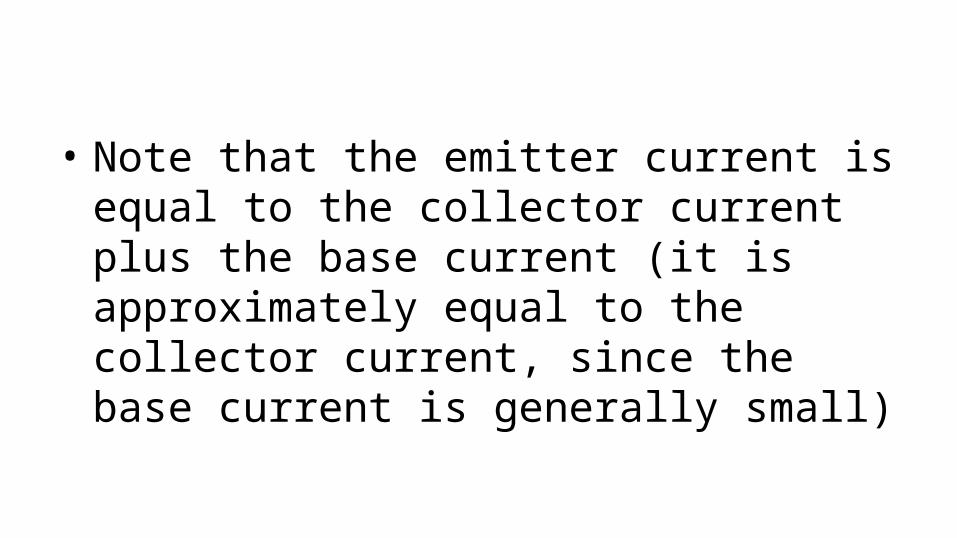
• Note that the emitter current is equal to the collector current plus the base current (it is approximately equal to the collector current, since the base current is generally small)
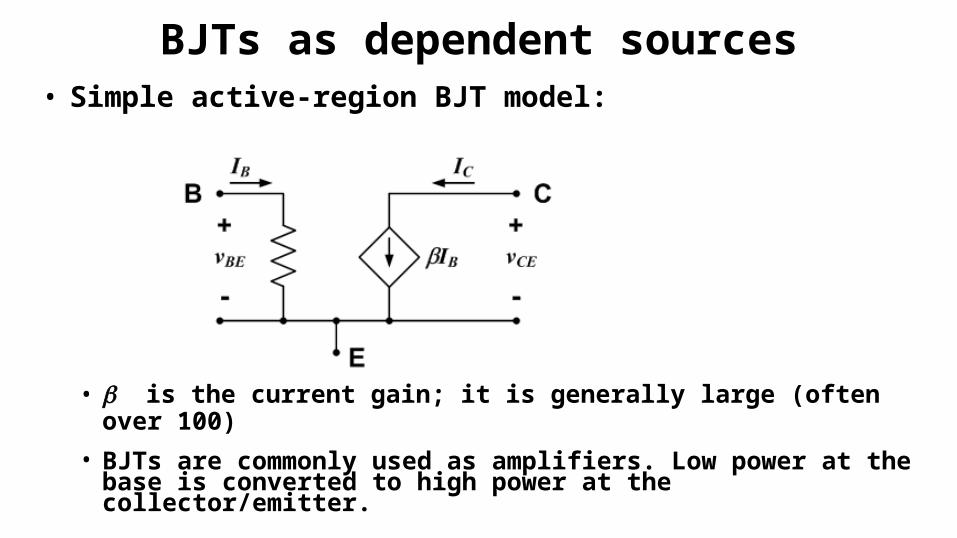
BJTs as dependent sources• Simple active-region BJT model:
• is the current gain; it is generally large (often over 100)• BJTs are commonly used as amplifiers. Low power at the
base is converted to high power at the collector/emitter.

• Demo:– Show BJTs– Illustrate change in emitter current with base current (voltage). Emphasize
external power supply.

Active circuit elements - operational amplifiers• Operational amplifier (or op-amp) based circuits are often
used to perform mathematical operations
• Operational amplifiers are constructed of a number of transistors, but are typically represented by the circuit symbol:
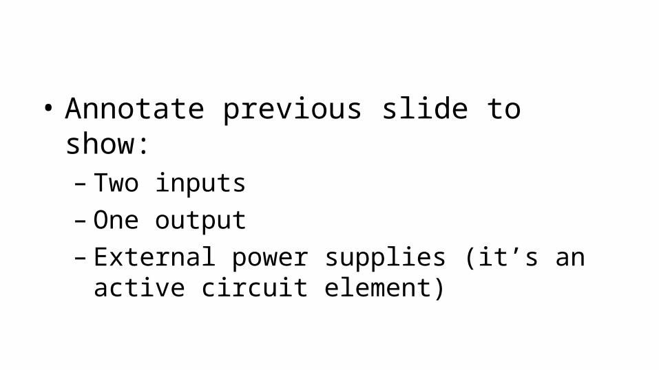
• Annotate previous slide to show:– Two inputs– One output– External power supplies (it’s an active circuit
element)

Notes about operational amplifiers• Op-amp circuits have two inputs and one output• Op-amps require (generally) two external power supply
inputs• There is (ideally) no current flow into the input
terminals• The op-amp absorbs no power from the circuit
• The output voltage is the difference in the input voltages, multiplied by a large number (ideally, infinity)• However, the output voltage cannot exceed the range set
by the external power supplies
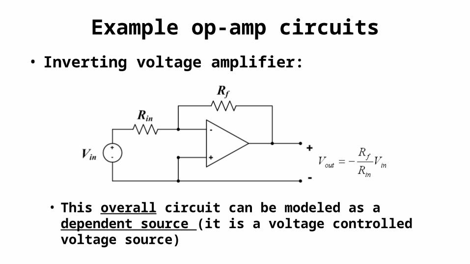
Example op-amp circuits
• Inverting voltage amplifier:
• This overall circuit can be modeled as a dependent source (it is a voltage controlled voltage source)
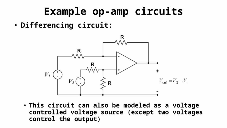
• Differencing circuit:
• This circuit can also be modeled as a voltage controlled voltage source (except two voltages control the output)
Example op-amp circuits
• Demo:– Show op-amp– Show op-amp circuits; emphasize external power supplies. Mention voltage
rails limit output voltages.