Lecture 9: Metal-semiconductor junctions - NPTEL · Lecture 9: Metal-semiconductor junctions...
16
Lecture 9: Metal-semiconductor junctions Contents 1 Introduction 1 2 Metal-metal junction 1 2.1 Thermocouples .......................... 2 3 Schottky junctions 4 3.1 Forward bias ............................ 9 3.2 Reverse bias ............................ 10 4 Ohmic junction 12 1 Introduction Formation of electronic devices requires putting together two or more dissim- ilar materials (semiconductors, metals, insulators). The interface between these materials becomes crucial because it affects the electrical properties (transport) of the devices. This interface is called the junction. An ideal junction is one where there are no defects formed at the interface. Forming ideal junctions is challenging and most real materials have defects at the in- terface which can affect the electronic properties. But we can get an idea of the interaction between materials by studying ideal junction. 2 Metal-metal junction Consider a junction formed between 2 metals with different work functions, as shown in figure 1. Metals are characterized by an incomplete energy band (valence and conduction band overlap) with the top of the energy band being 1
Transcript of Lecture 9: Metal-semiconductor junctions - NPTEL · Lecture 9: Metal-semiconductor junctions...

Lecture 9: Metal-semiconductorjunctions
Contents
1 Introduction 1
2 Metal-metal junction 12.1 Thermocouples . . . . . . . . . . . . . . . . . . . . . . . . . . 2
3 Schottky junctions 43.1 Forward bias . . . . . . . . . . . . . . . . . . . . . . . . . . . . 93.2 Reverse bias . . . . . . . . . . . . . . . . . . . . . . . . . . . . 10
4 Ohmic junction 12
1 Introduction
Formation of electronic devices requires putting together two or more dissim-ilar materials (semiconductors, metals, insulators). The interface betweenthese materials becomes crucial because it affects the electrical properties(transport) of the devices. This interface is called the junction. An idealjunction is one where there are no defects formed at the interface. Formingideal junctions is challenging and most real materials have defects at the in-terface which can affect the electronic properties. But we can get an idea ofthe interaction between materials by studying ideal junction.
2 Metal-metal junction
Consider a junction formed between 2 metals with different work functions,as shown in figure 1. Metals are characterized by an incomplete energy band(valence and conduction band overlap) with the top of the energy band being
1

MM5017: Electronic materials, devices, and fabrication
Figure 1: Junction between Mo and Pt. Mo has a smaller work function thanPt. When a junction is formed electrons from Mo move to Pt until the Fermilevel lines up and the junction is in equilibrium. Adapted from Principles ofElectronic Materials - S.O. Kasap.
the Fermi energy. The distance from the Fermi level to the vacuum level iscalled the work function (φ). In figure 1 the two metals are Pt and Mowith work functions of 5.36 and 4.20 eV respectively. Actual junctions areformed usually by vapor deposition of one metal on top of the other. Usuallysome form of post deposition annealing is also used to form the interface andreduce defect density.The most important rule when a junction is formed is that the Fermi levelsmust line up at equilibrium (no external bias). This can be understood byusing figure 1, where there are electrons in Mo at a higher energy level thanthose in Pt. These electrons can occupy the empty energy levels locatedabove the Pt Fermi level. Because electrons move from Mo to Pt a netpositive charge develops on the Mo side and a net negative charge on thePt side. Thus, a contact potential is developed at equilibrium between thetwo metals. This contact potential is related to the difference in the workfunctions, and is shown in figure 2. For Mo-Pt junction the contact potentialis 1.16 V .
2.1 Thermocouples
Metal-metal junctions are used to form thermocouples, which are used foraccurate temperature measurements. Thermocouples are an example of tem-perature measurement by a contact technique, while pyrometers are examples
2

MM5017: Electronic materials, devices, and fabrication
Figure 2: Junction formed between Mo and Pt at equilibrium, with a contactpotential given by the difference between the work functions. The contactpotential prevents further motion of electrons from Mo to Pt. Adapted fromPrinciples of Electronic Materials - S.O. Kasap.
of non-contact temperature measurement. To understand the working of athermocouple we need to consider the Seeback effect , summarized in figure 3.When a metal is heated at one end and the other end is kept cold, electronsat the hot end are more energetic than those at the cold end. These electronshave a greater thermal velocity and can move towards the cold end. Thiscreates a potential within the metal with the hot end at a positive potentialwith respect to the cold end, see figure 3. The potential created is called theSeeback potential and it depends on the temperature difference between thehot and cold end.
∆V =
∫ T2
T1
S∆T (1)
S is called the Seeback coefficient and is a material dependent parameterand also a function of temperature. The Seeback coefficient is approximatelyrelated to the Fermi energy by the Mott and Jones equation, which is validfor a larger number of metals.
S ≈ π2k2BT
3eEF
x (2)
x here is a numerical constant that depends on the charge transport proper-ties of the metal. Seeback coefficient values for different metals are listed in
3

MM5017: Electronic materials, devices, and fabrication
Figure 3: Schematic of the Seeback effect showing the potential developmentin a metal with a temperature gradient. There is a greater energy of electronsat the hot end which then flow to the cold end leasing to development onan in-built potential. The potential depends on the temperature differenceand a material parameter called the Seeback coefficient. Adapted fromPrinciples of Electronic Materials - S.O. Kasap.
table 1.If a junction is formed between two dissimilar materials and one end is
placed at the hot end (e.g. a furnace whose temperature is to be measured)and the other end placed at the cold end (room temperature) then a contactpotential is developed at both ends. This contact potential is different sincethe Seeback coefficients of the two materials are different. So a net potentialdevelops in the system given by
∆V =
∫ T2
T1
(SA − SB)∆T (3)
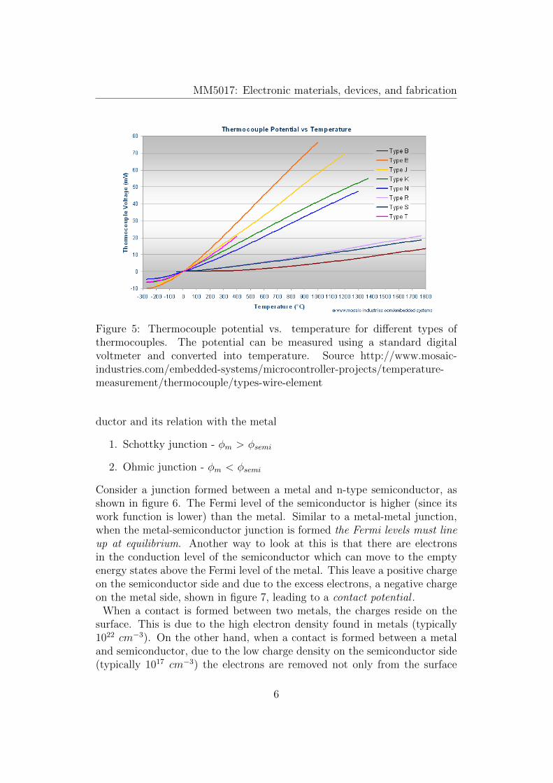
where SA and SB are the Seeback coefficients of the two metals. The setupis shown schematically in figure 4. Typically, thermocouple potentials aretabulated for different temperatures for standard thermocouple materials.These tables are used when measuring the temperature of the unknown sam-ple. There are different thermocouples used for specific temperature regions,as shown in figure 5.
3 Schottky junctions
When a metal and semiconductor are brought into contact, there are twotypes of junctions formed depending on the work function of the semicon-
4

MM5017: Electronic materials, devices, and fabrication
Table 1: Seeback coefficients for some typical metals at two different tem-peratures and values for x. The EF values are also listed. Adapted fromPrinciples of Electronic Materials - S.O. Kasap.
Metal S at 273 K S at 300 K EF x(µV K−1) (µV K−1) (eV )
Al -1.6 -1.8 11.6 2.78Au 1.79 1.94 5.5 -1.48Cu 1.70 1.84 7.0 -1.79K -12.5 2.0 3.8Li 14 4.7 -9.7Mg -1.3 3.2 1.38Na -5 3.1 2.2
Figure 4: Temperature measurements using a thermocouple consisting of towdissimilar metals. There is a potential difference at the two junctions arisingfrom the different Seeback coefficients of the two materials. Adapted fromPrinciples of Electronic Materials - S.O. Kasap.
5
MM5017: Electronic materials, devices, and fabrication
Figure 5: Thermocouple potential vs. temperature for different types ofthermocouples. The potential can be measured using a standard digitalvoltmeter and converted into temperature. Source http://www.mosaic-industries.com/embedded-systems/microcontroller-projects/temperature-measurement/thermocouple/types-wire-element
ductor and its relation with the metal
1. Schottky junction - φm > φsemi
2. Ohmic junction - φm < φsemi
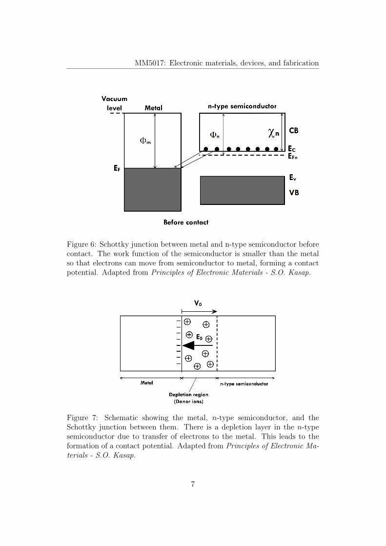
Consider a junction formed between a metal and n-type semiconductor, asshown in figure 6. The Fermi level of the semiconductor is higher (since itswork function is lower) than the metal. Similar to a metal-metal junction,when the metal-semiconductor junction is formed the Fermi levels must lineup at equilibrium. Another way to look at this is that there are electronsin the conduction level of the semiconductor which can move to the emptyenergy states above the Fermi level of the metal. This leave a positive chargeon the semiconductor side and due to the excess electrons, a negative chargeon the metal side, shown in figure 7, leading to a contact potential .
When a contact is formed between two metals, the charges reside on thesurface. This is due to the high electron density found in metals (typically1022 cm−3). On the other hand, when a contact is formed between a metaland semiconductor, due to the low charge density on the semiconductor side(typically 1017 cm−3) the electrons are removed not only from the surface
6
MM5017: Electronic materials, devices, and fabrication
Figure 6: Schottky junction between metal and n-type semiconductor beforecontact. The work function of the semiconductor is smaller than the metalso that electrons can move from semiconductor to metal, forming a contactpotential. Adapted from Principles of Electronic Materials - S.O. Kasap.
Figure 7: Schematic showing the metal, n-type semiconductor, and theSchottky junction between them. There is a depletion layer in the n-typesemiconductor due to transfer of electrons to the metal. This leads to theformation of a contact potential. Adapted from Principles of Electronic Ma-terials - S.O. Kasap.
7

MM5017: Electronic materials, devices, and fabrication
Figure 8: Schottky junction showing the band bending on the semiconductorside. Semiconductor bands bend up going from the semiconductor (posi-tive) to metal (negative) since this is the same direction as the electric field.Adapted from Principles of Electronic Materials - S.O. Kasap.
but also from a certain depth within the semiconductor. This leads to theformation of a depletion region within the semiconductor, shown in fig-ure 7.Thus, when a Schottky junction is formed between the metal and semicon-ductor, the Fermi level lines up and also a positive potential is formed on thesemiconductor side. Because the depletion region extends within a certaindepth in the semiconductor there is bending of the energy bands on the semi-conductor side. Bands bend up in the direction of the electric field (field goesfrom positive charge to negative charge, opposite of the potential direction).This means the energy bands bend up going from n-type semiconductor tometal, shown in figure 8. The Fermi levels line up and there is a certainregion in the semiconductor (denoted by W ) where the bands bend (this isthe depletion region). Another name for the depletion region is the spacecharge layer.There is a built in potential in the Schottky junction, V0, and from figure 8this is given by the difference in work functions.
eV0 = φm − φsemi (4)
The work function of the metal is a constant while the semiconductor workfunction depends on the dopant concentration (since this affects the Fermi
8

MM5017: Electronic materials, devices, and fabrication
level position). The contact potential then represents the barrier for theelectrons to move from the n-type semiconductor to the metal. Initially, whenthe junction is formed electrons move to the metal to create the depletionregion. The contact potential thus formed prevents further motion of theelectrons to the metal.There is also a barrier for electrons to move frommetal to semiconductor. This is called the Schottky barrier and denotedby φB in figure 8. This is given by
φB = (φm − φn) + (Ec − EFn) = φm − χn (5)
where χn is the electron affinity of the n-type semiconductor.At equilibrium the motion of electrons from the semiconductor to metal isbalanced by the contact potential so that there is no net current. The Schot-tky junction can be biased by application of an external potential. There aretwo types of bias
1. Forward bias - metal is connected to positive terminal and n-type semi-conductor connected to negative terminal
2. Reverse bias - metal is connected to negative terminal and n-type semi-conductor connected to positive terminal
The current flow depends on the type of bias and the amount of appliedexternal potential.
3.1 Forward bias
In a forward biased Schottky junction the external potential is applied insuch a way that it opposes the in-built potential. Since the region with thehighest resistivity is the depletion region near the junction, the voltage dropis across the depletion region. Under external bias the Fermi levels no longerline up, but are shifted with respect to one another and the magnitude of theshift depends on the applied voltage. Energy band diagram of the Schottkyjunction under forward bias is shown in figure 9. Thus, electrons injectedfrom the external circuit into the n-type semiconductor have a lower barrierto surmount before reaching the metal. This leads to a current in the circuitwhich increases with increasing external potential. The current in a Schottkydiode under forward bias is given by
J = J0 [exp(eV
kBT) − 1] (6)
where J is the current density for an applied potential of V . J0 is a constantand depends on the Schottky barrier (φB) for the system and the expression
9

MM5017: Electronic materials, devices, and fabrication
Figure 9: Schottky junction under forward bias. Adapted from Principles ofElectronic Materials - S.O. Kasap.
is
J0 = AT 2 exp(− φB
kBT) (7)
where A is the Richardson constant for thermionic emission and is a materialproperty. Equation 6 shows that in the forward bias the current exponentiallyincreases with applied potential.
3.2 Reverse bias
In the case of a reverse bias the external potential is applied in the same di-rection as the junction potential, as shown in figure 10. Once again the Fermilevels no longer line up but the barrier for electron motion from the n-typesemiconductor to metal becomes higher. The electron flow is now from themetal to the semiconductor and the barrier for this is given by the Schottkybarrier (φB). So there is a constant current in reverse bias, whose magnitudeis equal to J0 (as given in equation 7). From calculations it can be shown thatthe current in the forward bias is orders of magnitude higher than the currentin reverse bias (this arises due to the exponential dependence on potential).So a Schottky junction acts as a rectifier i.e. it conducts in forward biasbut not in reverse bias. The I −V characteristics of the junction is shown infigure 11. There is an exponential increase in current in the forward bias (Iquadrant) while there is a small current in reverse bias (IV quadrant).
10

MM5017: Electronic materials, devices, and fabrication
Figure 10: Schottky junction under reverse bias. Adapted from Principlesof Electronic Materials - S.O. Kasap.
Figure 11: I − V characteristics of a Schottky junction showing rectifyingproperties. Adapted from Principles of Electronic Materials - S.O. Kasap.
11

MM5017: Electronic materials, devices, and fabrication
Figure 12: I − V characteristics of a Schottky junction between n-Si andAu. The barrier potential energy is 0.83 eV and the Richardson constantis 110 Acm−2K−2. The plot is at room temperature and generated usingMATLAB. The y-axis is in mA in the forward bias quadrant and µA in thereverse bias quadrant.
The forward and reverse bias currents for a Schottky junnction formed be-tween Si and Au can be calculated using equations 6 and 7. Consider n-typeSi with donor concentration of 1016 cm−3. The dopant concentration fixes theFermi level position in the semiconductor and hence its work function. ForAu-Si the measured value of the Schottky barrier is 0.83 eV . The Richardsonconstant for this junction is 110 Acm−2K−2. Using equation 7 it is possi-ble to calculate the reverse saturation current density in this junction. Thisis a constant, independent of the reverse bias voltage, and has a value of0.12 µAcm−2. The forward bias current density depends on the applied volt-age, equation 6, and increases exponentially with the applied voltage. TheI-V characteristics of this junction is plotted in figure 12. The plot is similarto that shown in figure 11, and rectification can be seen from the fact thatforward bias current is more than three orders of magnitude higher than thereverse bias current and the value increases with applied voltage.
4 Ohmic junction
A Schottky junction is formed when the semiconductor has a lower work func-tion than the metal. When the semiconductor has a higher work functionthe junction formed is called the Ohmic junction. Once again it is possi-ble to draw the energy band diagram of the junction in equilibrium (Fermilevels line up). This is shown in figure 13. At equilibrium, electrons move
12

MM5017: Electronic materials, devices, and fabrication
Figure 13: Ohmic junction (a) before and (b) after contact. Before contactsthe Fermi levels are at different positions and they line up on contact to givean accumulation region in the semiconductor. Adapted from Principles ofElectronic Materials - S.O. Kasap.
from the metal to the empty states in the conduction band so that there isan accumulation region near the interface (on the semiconductor side). Theaccumulation region has a higher conductivity than the bulk of the semicon-ductor due to this higher concentration of electrons. Thus, a Ohmic junctionbehaves as a resistor conducting in both forward and reverse bias. The re-sistivity is determined by the bulk resistivity of the semiconductor.One of the interesting applications of Ohmic junctions is in thermoelectricdevices, where a small volume can be cooled by application of direct currents.For Ohmic junctions, depending on the direction of current flow (forward orreverse biass), heat can be generated or absorbed. This is shown in figure 14.This is called Peltier effect and is applicable to junctions between any twodissimilar materials. So, when current flows through a metal semiconductorOhmic junction, heat will always be released or absorbed. This can be usedas a practical cooling device, as shown in the schematic in figure 15. Both p-and n- type semiconductors are used and the current flow is such that oneend is always cold (heat absorbed) while the other end is hot (heat released).There are different metals that form Ohmic contacts with semiconductors.A partial list of such combinations is shown in table 2. This list is importantbecause it gives the acceptable metals for each semiconductor that can beused in fabrication of devices. For Si, earlier Al was used for making elec-trical contacts, which was then replaced by Al-Cu alloys. Both form Ohmiccontacts with Si. These have now been replaced by Cu (higher conductiv-ity). But, Cu is poisonous to Si and hence cannot directly come into contactwith the semiconductor. Usually, Ti or TiN is used to make electrical con-
13

MM5017: Electronic materials, devices, and fabrication
Figure 14: Current flow through an Ohmic junction can lead to heat (a)absorption or (b) release. This depends on the external bias, that determinesthe direction of heat flow. When electrons move from metal to higher energylevels in the semiconductor heat is absorbed and the reverse happens whenelectrons flow from semiconductor to metal. Adapted from Principles ofElectronic Materials - S.O. Kasap.
14

MM5017: Electronic materials, devices, and fabrication
Figure 15: Schematic of the Peltier cooler using both p- and n- type semi-conductors. One end of the cooler is connected to the body from which heatis absorbed (cooled) and the other end is connected to a heat sink, where itis released. Adapted from Principles of Electronic Materials - S.O. Kasap.
15

MM5017: Electronic materials, devices, and fabrication
Table 2: Combination of semiconductors (n and p) and metals (alloys) thatnormally form Ohmic contacts. Adapted from Principles of Electronic Ma-terials - S.O. Kasap.
n-semiconductor Metal p-semiconductor MetalGe Al, Au, Bi,
Sb, SnGe Ag, Al, Au,
Cu, Ga, In,Ni, Pt, Sn
Si Ag, Al, Ni,Sn, In, Sb, Ti,TiN
Si Ag, Al, Au,Ni, Pt, Sn, In,Pb, Ga, Ge,Ti, TiN
GaAs Ag-Sn GaAs Ag-ZnGaP Al, Au-Si,
Au-Sn, In-SnGaP Au-Zn, Ga,
Zn, Ag-ZnGaAsP Au-Sn GaAsP Au-ZnGaAlAs Au-Ge-Ni GaAlAs Au-ZnInAs Au-Ge, Sn InAs AlInGaAs Au-Ge, Ni InGaAs Au-Zn, NiCdS Ag, Al, Au,
Ga, InCdTe In CdTe Au, In-Ni, Pt,
RhZnSe In, In-Ga, PtSiC W SiC Al-Si, Si, Ni
tact with Si, and then Cu is deposited. Ti or TiN is chosen because it alsoforms Ohmic contacts with p and n type Si, see table 2, and can be eas-ily deposited by chemical vapor deposition. For integrated devices electricalcontacts to the outside circuit components are done using evaporated met-als and Ohmic contacts are formed. This is because the electrical contactshould not impose a rectifying behavior on the device. Thermal processingof metal-semiconductor contacts can lead to inter-diffusion and formation ofmetal silicides. Pt-Si forms a number of silicide phases like PtSi, Pt2Si, andPt3Si. Similarly, Ti-Si forms TiSi2, Ti2Si, and Ti3Si. Thus the contact is nolonger between a metal-semiconductor but between a silicide-semiconductor.This can affect the electrical properties of the junction.
16