Lecture 8: Latch and Flip Flop Design - stanford.edu EE371 3 Recent Interest in Flip-Flops •Trends...
34
4/24/02 EE371 1 Lecture 8: Latch and Flip Flop Design Slides originally from: Vladimir Stojanovic & Vojin G. Oklobdzija Computer Systems Laboratory Stanford University [email protected]
Transcript of Lecture 8: Latch and Flip Flop Design - stanford.edu EE371 3 Recent Interest in Flip-Flops •Trends...
4/24/02 EE371 1
Lecture 8:Latch and Flip Flop Design
Slides originally from:Vladimir Stojanovic & Vojin G. Oklobdzija
Computer Systems LaboratoryStanford University

4/24/02 EE371 2
Outline
• Recent interest in latches and flip-flops
• Timing and Power metrics
• Design and optimization tradeoffs
• Master-slave vs. Pulse-triggered Latch
• Representative designs
• Comparison
4/24/02 EE371 3
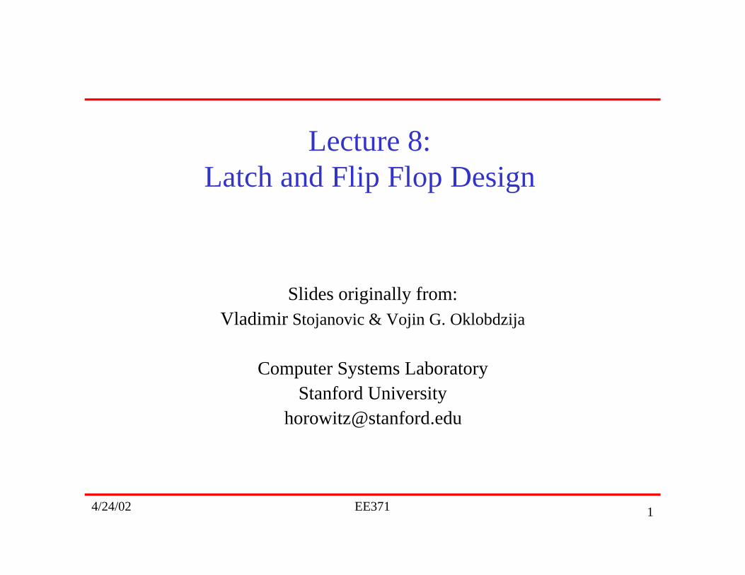
Recent Interest in Flip-Flops• Trends in high-performance systems
Higher clock frequency
More transistors on chip
• ConsequencesIncreased flip-flop overhead relative to cycle time
• Cycle time 10 - 20 FO4 delays, flop overhead 2 - 4 FO4
Difficult to control both edges of the clock
Higher impact of clock skew
Higher crosstalk and substrate coupling
Higher power consumption• expensive packages and cooling systems
• limit in performance
Clock burns up to 40%, flops up to 20% of total power
4/24/02 EE371 4
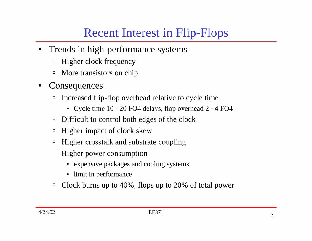
Requirements in the Flip-Flop Design
• Small Clk-Output delay, Narrow sampling window
• Low power
• Small clock load
• High driving capability (increased levels of parallelism)Typical flip-flop load in a 0.18µm CMOS ranges from 50fF toover 200fF, with typical values of 100-150fF in critical paths
• Integration of logic into the flop
• Multiplexed or clock scan
• Crosstalk insensitivity- dynamic/high impedance nodes are affected
4/24/02 EE371 5
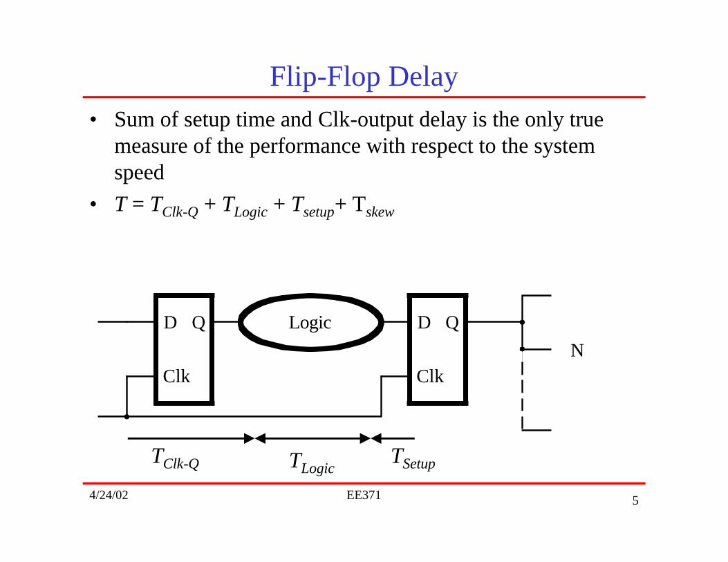
Flip-Flop Delay• Sum of setup time and Clk-output delay is the only true
measure of the performance with respect to the systemspeed
• T = TClk-Q + TLogic + Tsetup+ Tskew
D Q
Clk
D Q
Clk
Logic
N
TLogicTClk-Q TSetup
4/24/02 EE371 6
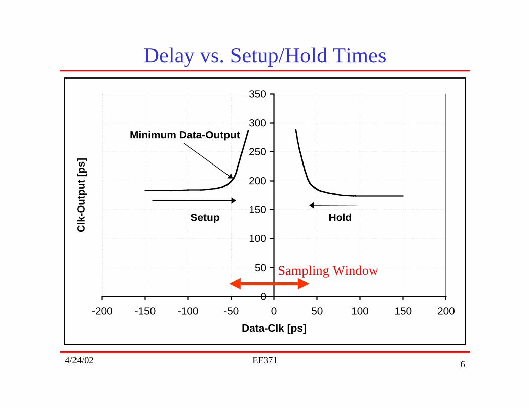
Delay vs. Setup/Hold Times
0
50
100
150
200
250
300
350
-200 -150 -100 -50 0 50 100 150 200
Data-Clk [ps]
Clk
-Ou
tpu
t [p
s]
Setup Hold
Minimum Data-Output
Sampling Window

4/24/02 EE371 7
Timing parameters, details
250
270
290
310
330
350
370
390
410
-80 -60 -40 -20 0 20 40 60 80 100
D - Clk delay [ps]
Tim
e [p
s]
Stable Clk-Q regionUnstable Clk-Q region
Fai
lure
reg
ion
Clk-Q stableminimum D-Q
Optimum setup time
D-Q
D CQ
U
D CQ+U
The best point to pick on delay curve is minimum D-Q
4/24/02 EE371 8
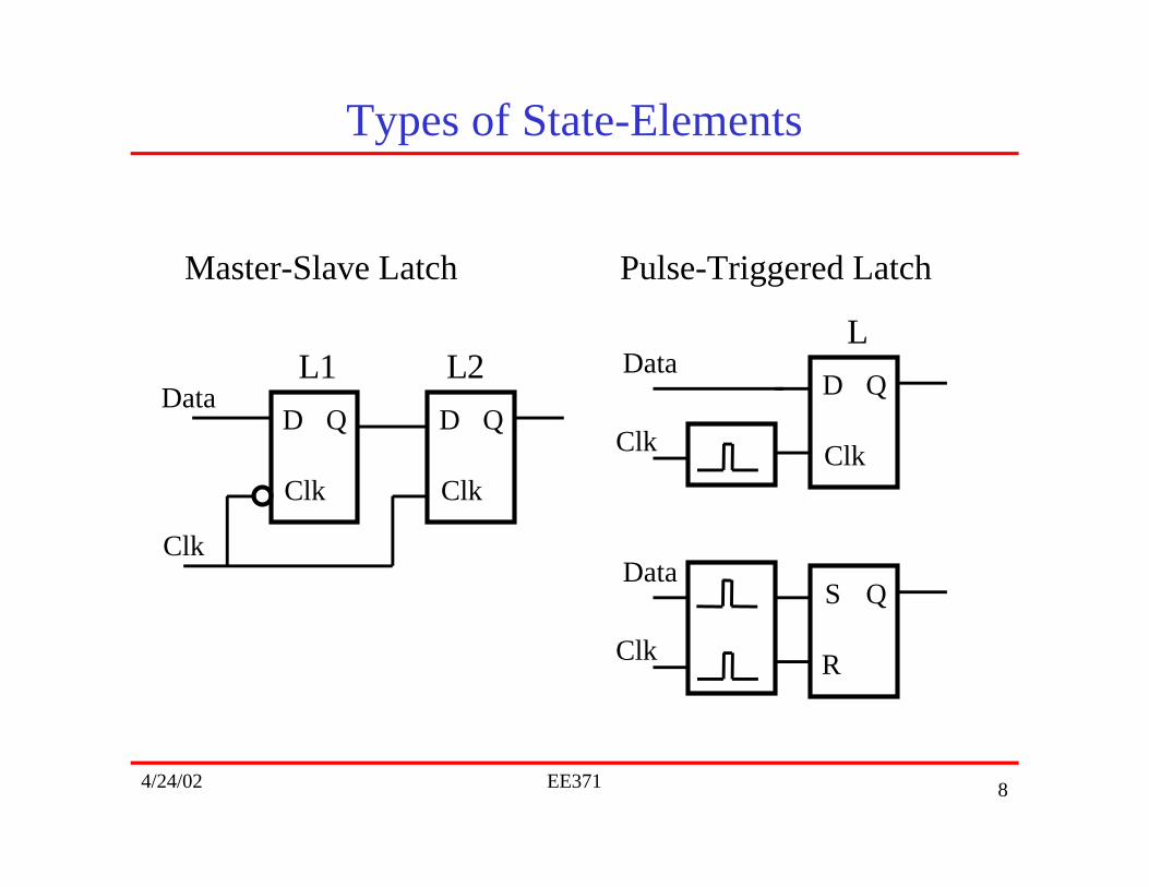
Types of State-Elements
Master-Slave Latch
D
Clk
Q D
Clk
Q
Clk
Data D
Clk
Q
Clk
Data
Pulse-Triggered Latch
L1 L2L
S
R
Q
Clk
Data

4/24/02 EE371 9
Master-Slave Latches
• Positive setup times
• Two clock phases:distributed globally
generated locally
• Small penalty in delay for incorporating MUX
• Some circuit tricks needed to reduce the overall delay
4/24/02 EE371 10
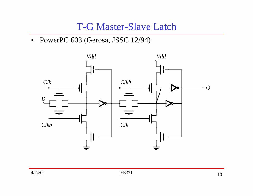
T-G Master-Slave Latch• PowerPC 603 (Gerosa, JSSC 12/94)
Vdd Vdd
Clk
QClk Clkb
Clkb
D
4/24/02 EE371 11
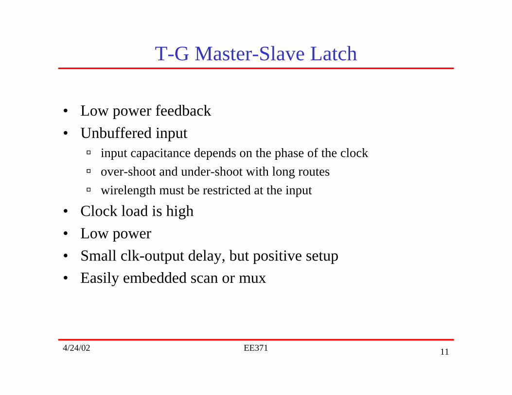
T-G Master-Slave Latch
• Low power feedback
• Unbuffered inputinput capacitance depends on the phase of the clock
over-shoot and under-shoot with long routes
wirelength must be restricted at the input
• Clock load is high
• Low power
• Small clk-output delay, but positive setup
• Easily embedded scan or mux
4/24/02 EE371 12
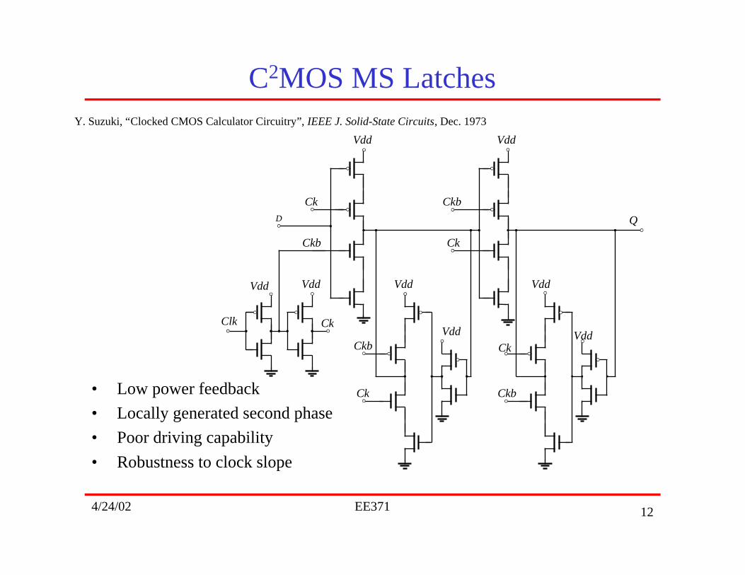
C2MOS MS Latches
• Low power feedback
• Locally generated second phase
• Poor driving capability
• Robustness to clock slope
VddVdd Vdd
Vdd
Vdd Vdd
Vdd
VddClk Ck
Ck
Ck
Ck
CkCkb
Ckb
Ckb
Ckb
QD
Y. Suzuki, “Clocked CMOS Calculator Circuitry”, IEEE J. Solid-State Circuits, Dec. 1973
4/24/02 EE371 13
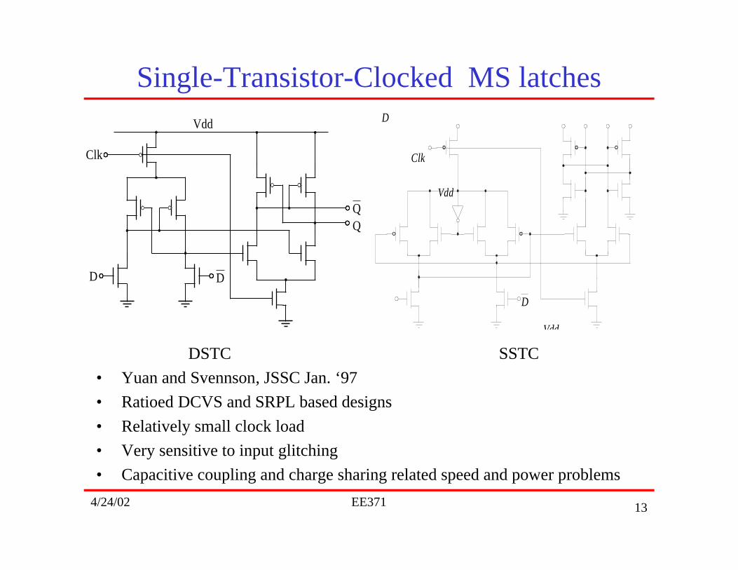
Single-Transistor-Clocked MS latches
Vdd
Vdd
Clk
D
D
DSTC SSTC
• Yuan and Svennson, JSSC Jan. ‘97
• Ratioed DCVS and SRPL based designs
• Relatively small clock load
• Very sensitive to input glitching
• Capacitive coupling and charge sharing related speed and power problems
DD
Vdd
Clk
4/24/02 EE371 14
Pulse-Triggered Latches
• First stage is a pulse generatorgenerates a pulse (glitch) on a rising edge of the clock
• Second stage is a latchcaptures the pulse generated in the first stage
• Pulse generation results in a negative setup time
• Frequently exhibit a soft edge property
• Must check for hold time violations
Note: power is always consumed in the clocked pulsegenerator

4/24/02 EE371 15
Hybrid Latch Flip-Flop (H. Partovi, ISSCC’96)
Vdd
D
Clk
Q
Q
D=1
D=0
signal atnode X
SecondStage Latch
Pulse Generator
D=1
D=0

4/24/02 EE371 16
HLFF – pulse generation
D=1
D=0signal atnode X
SecondStage Latch
PulseGenerator
D=1
D=0
Clk
Data
Keepers
4/24/02 EE371 17
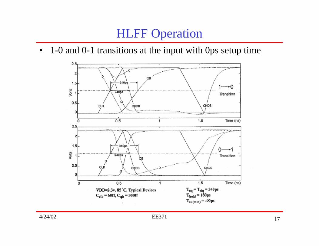
HLFF Operation• 1-0 and 0-1 transitions at the input with 0ps setup time
4/24/02 EE371 18
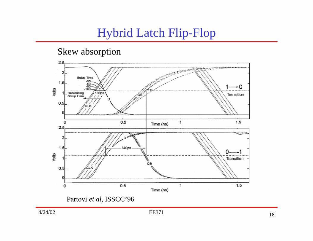
Hybrid Latch Flip-Flop
Partovi et al, ISSCC’96
Skew absorption
4/24/02 EE371 19
Hybrid Latch Flip-Flop• Flip-flop features:
single phase clock
edge triggered, on one clock edge
• Latch features: Soft clock edge propertybrief transparency, equal to 3 inverter delays
negative setup time
allows slack passing
absorbs skew
• Hold time is comparable to HLFF delayminimum delay between flip-flops must be controlled
• Fully static
• Possible to incorporate logic

4/24/02 EE371 20
Semi-Dynamic Flip-Flop (SDFF)• Sun UltraSparc III, Klass, VLSI Circuits’98
• Soft edge conditioned by data since first stage is precharged - cross-coupledlatch is added for robustness
• Small penalty for adding logic
• Latch has one transistor less in stack - faster than HLFF, but 1-1 glitch exists
Clk
D
Vdd Vdd
Q
Q
4/24/02 EE371 21
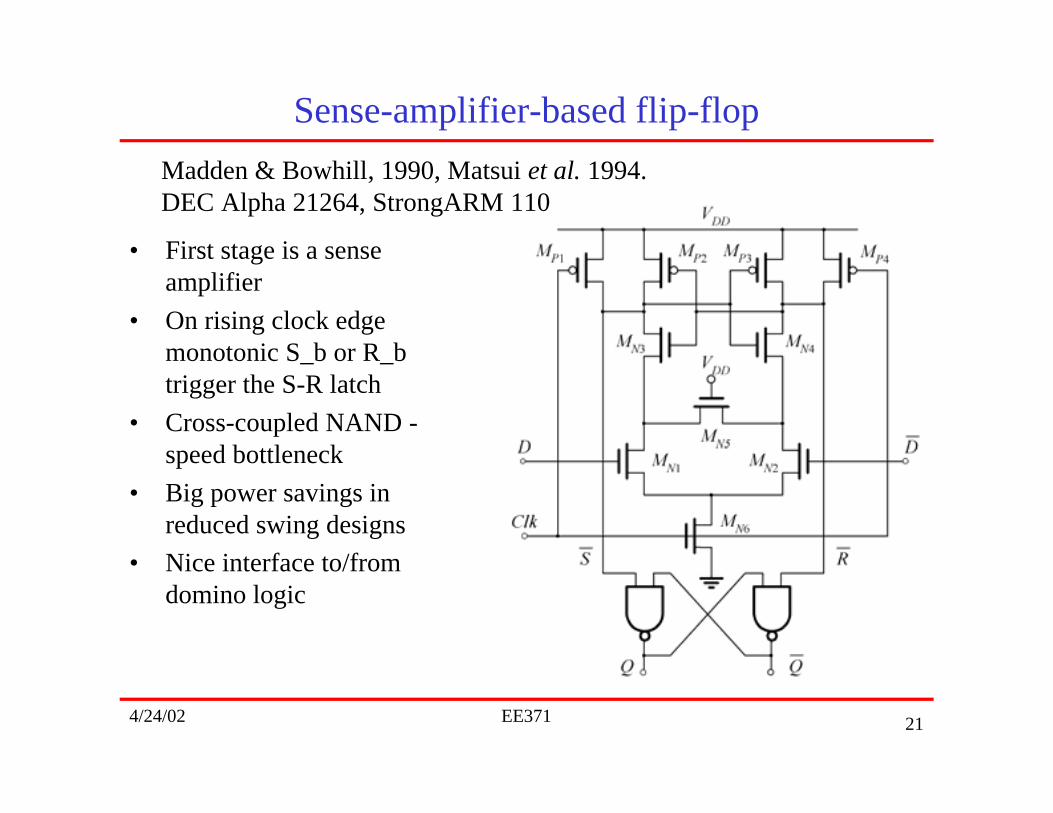
Sense-amplifier-based flip-flop
• First stage is a senseamplifier
• On rising clock edgemonotonic S_b or R_btrigger the S-R latch
• Cross-coupled NAND -speed bottleneck
• Big power savings inreduced swing designs
• Nice interface to/fromdomino logic
Madden & Bowhill, 1990, Matsui et al. 1994.DEC Alpha 21264, StrongARM 110
4/24/02 EE371 22
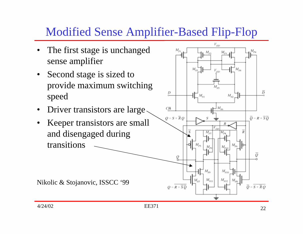
Modified Sense Amplifier-Based Flip-Flop
• The first stage is unchangedsense amplifier
• Second stage is sized toprovide maximum switchingspeed
• Driver transistors are large
• Keeper transistors are smalland disengaged duringtransitions
Nikolic & Stojanovic, ISSCC ‘99
4/24/02 EE371 23
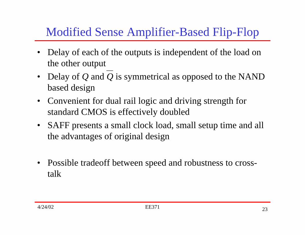
Modified Sense Amplifier-Based Flip-Flop
• Delay of each of the outputs is independent of the load onthe other output
• Delay of Q and Q is symmetrical as opposed to the NANDbased design
• Convenient for dual rail logic and driving strength forstandard CMOS is effectively doubled
• SAFF presents a small clock load, small setup time and allthe advantages of original design
• Possible tradeoff between speed and robustness to cross-talk
4/24/02 EE371 24
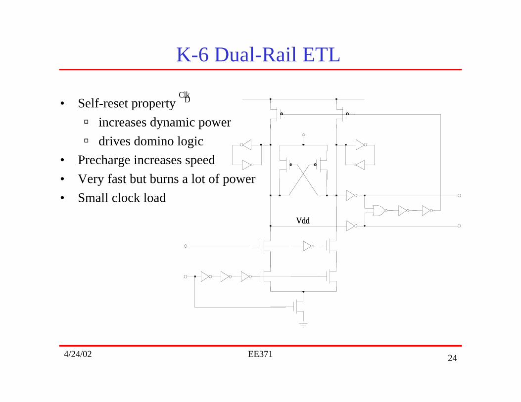
K-6 Dual-Rail ETL
DClk
VddVdd
• Self-reset property
increases dynamic power
drives domino logic
• Precharge increases speed
• Very fast but burns a lot of power
• Small clock load
4/24/02 EE371 25
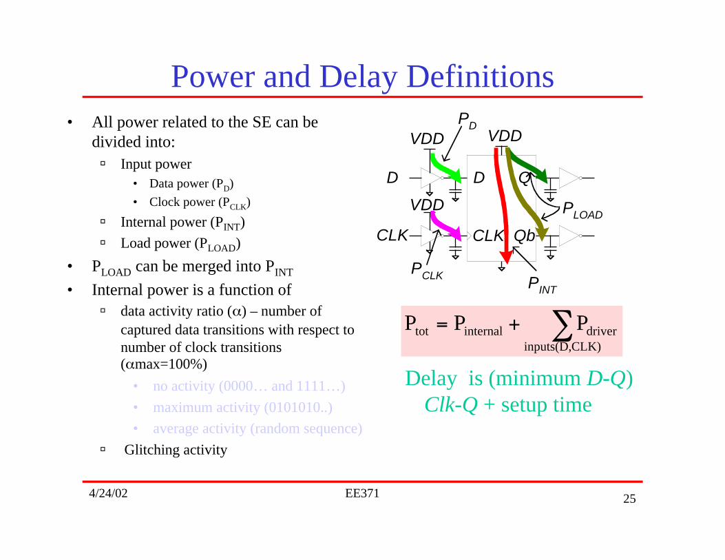
Power and Delay Definitions• All power related to the SE can be
divided into:Input power
• Data power (PD)
• Clock power (PCLK)
Internal power (PINT)
Load power (PLOAD)
• PLOAD can be merged into PINT
• Internal power is a function ofdata activity ratio (α) – number ofcaptured data transitions with respect tonumber of clock transitions(αmax=100%)
• no activity (0000… and 1111…)
• maximum activity (0101010..)
• average activity (random sequence)
Glitching activity
Q
CLK
D
Qb
VDDVDD
VDD
PD
PCLK PINT
PLOAD
D
CLK
∑+=CLK)inputs(D,
driverinternaltot PPP
Delay is (minimum D-Q)Clk-Q + setup time
4/24/02 EE371 26
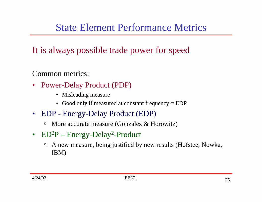
State Element Performance Metrics
It is always possible trade power for speed
Common metrics:
• Power-Delay Product (PDP)• Misleading measure
• Good only if measured at constant frequency = EDP
• EDP - Energy-Delay Product (EDP)More accurate measure (Gonzalez & Horowitz)
• ED2P – Energy-Delay2-ProductA new measure, being justified by new results (Hofstee, Nowka,IBM)
4/24/02 EE371 27
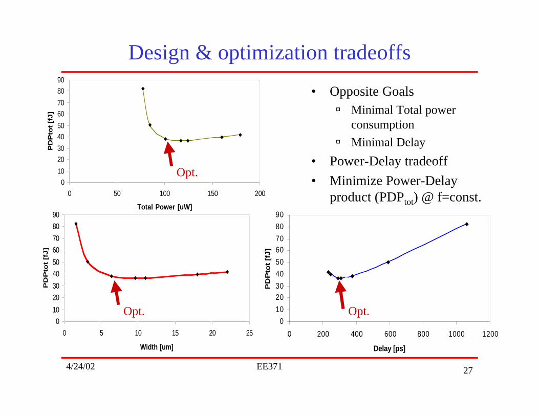
Design & optimization tradeoffs
• Opposite GoalsMinimal Total powerconsumption
Minimal Delay
• Power-Delay tradeoff
• Minimize Power-Delayproduct (PDPtot) @ f=const.
0
10
20
30
40
50
60
70
80
90
0 50 100 150 200
Total Power [uW]
PD
Pto
t [f
J]
0
10
20
30
40
50
60
70
80
90
0 200 400 600 800 1000 1200
Delay [ps]
PD
Pto
t [f
J]
0
10
20
30
40
50
60
70
80
90
0 5 10 15 20 25
Width [um]
PD
Pto
t [f
J]
Opt. Opt.
Opt.

4/24/02 EE371 28
Overall ResultsDelay Comparison (50% activity)
0
0.5
1
1.5
2
2.5
3
3.5
4
4.5
5
PowPC C2MOS HLFF SDFF StrongArm SAbFF
Dela
y [
FO
4 ]
Pulsed Latch DifferentialMS Latch
4/24/02 EE371 29
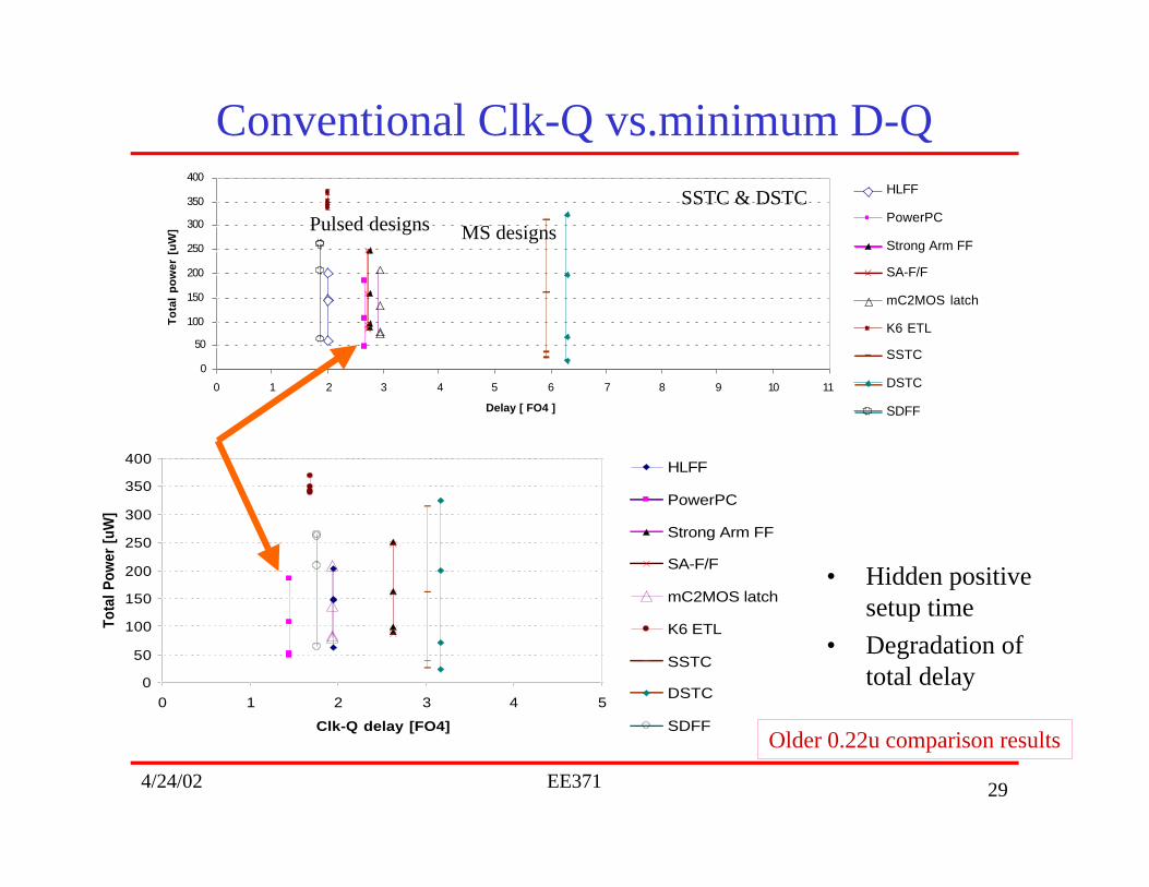
Conventional Clk-Q vs.minimum D-Q
• Hidden positivesetup time
• Degradation oftotal delay
0
50
100
150
200
250
300
350
400
0 1 2 3 4 5 6 7 8 9 10 11
Delay [ FO4 ]
To
tal
po
we
r [u
W]
HLFF
PowerPC
Strong Arm FF
SA-F/F
mC2MOS latch
K6 ETL
SSTC
DSTC
SDFF
0
50
100
150
200
250
300
350
400
0 1 2 3 4 5
Clk-Q delay [FO4]
Tota
l Pow
er [
uW]
HLFF
PowerPC
Strong Arm FF
SA-F/F
mC2MOS latch
K6 ETL
SSTC
DSTC
SDFF
SSTC & DSTCPulsed designs MS designs
Older 0.22u comparison results

4/24/02 EE371 30
Overall ResultsSingle-Edge Triggered Structures Power Consumption Comparison (50% activity)
0
50
100
150
200
250
PowPC
C2MO
S
DSTC
SSTC
HLFF
SDFFSE C
CFFTG
CPFF
Strong
Arm
SAbFF
DE CCFF
Po
we
r C
on
su
mp
tio
n [
uW
]
Internal Power [uW] Clock Power [uW] Data Power [uW]
Single Ended Dual EndedMS Latch
4/24/02 EE371 31
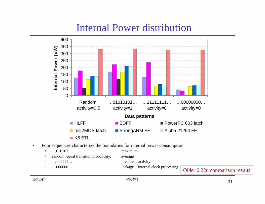
Internal Power distribution
• Four sequences characterize the boundaries for internal power consumption…010101… maximumrandom, equal transition probability, average…111111… precharge activity…000000… leakage + internal clock processing
0
50
100
150
200
250
300
350
400
Random,activity=0.5
…01010101…activity=1
…11111111…activity=0
…00000000…activity=0
Data patterns
Inte
rna
l P
ow
er
[uW
]
HLFF SDFF PowerPC 603 latch
mC2MOS latch StrongARM FF Alpha 21264 FF
K6 ETL
Older 0.22u comparison results
4/24/02 EE371 32
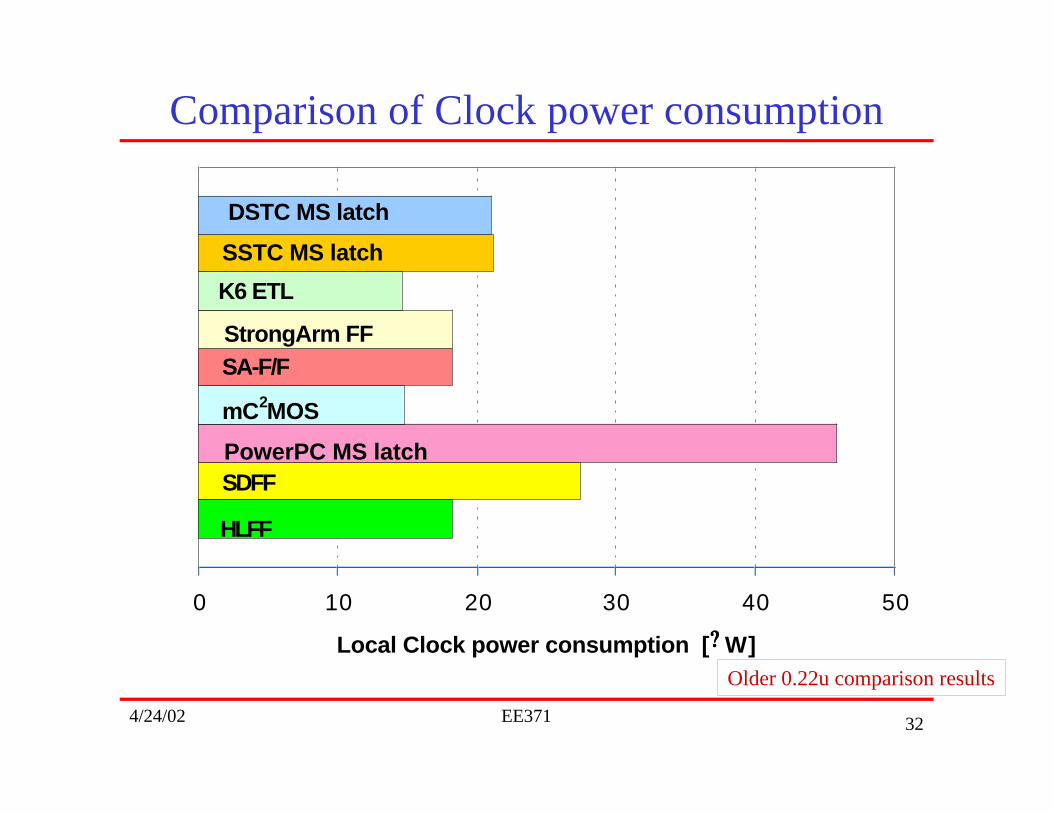
Comparison of Clock power consumption
0 10 20 30 40 50
Local Clock power consumption [???? W]
DSTC MS latch
SSTC MS latch
K6 ETL
StrongArm FF
SA-F/F
mC2MOS
PowerPC MS latchSDFF
HLFF
Older 0.22u comparison results
4/24/02 EE371 33
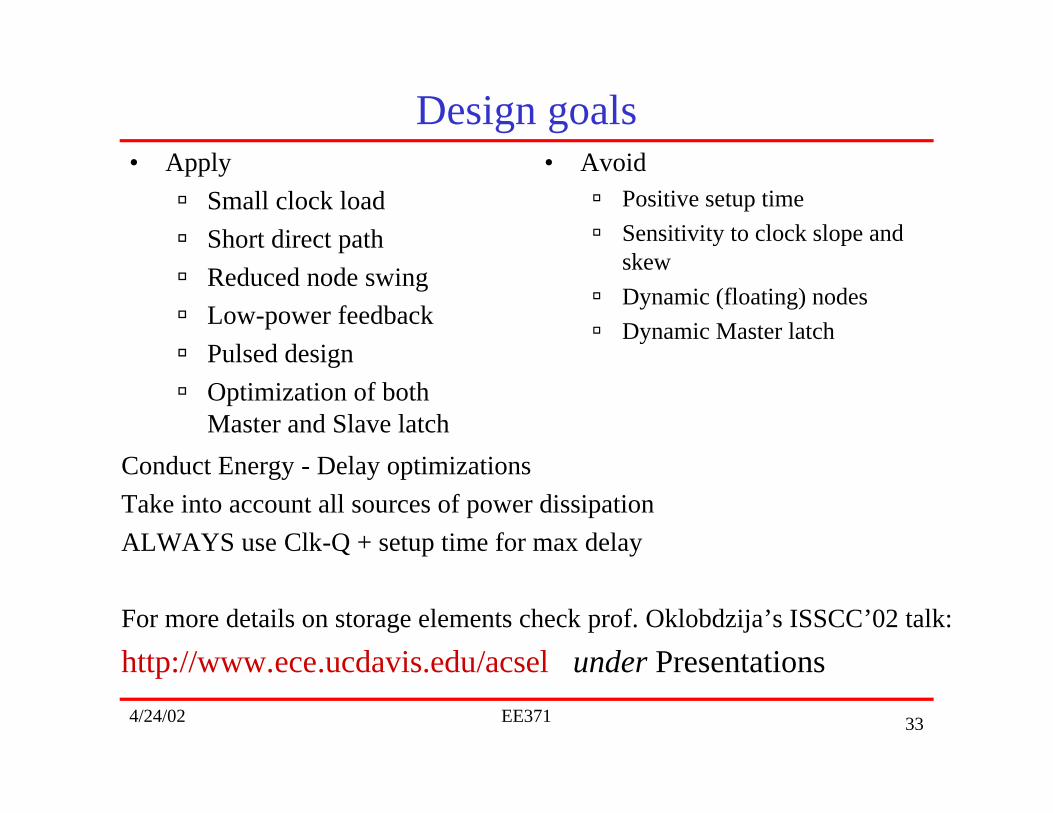
Design goals• Apply
Small clock load
Short direct path
Reduced node swing
Low-power feedback
Pulsed design
Optimization of bothMaster and Slave latch
• AvoidPositive setup time
Sensitivity to clock slope andskew
Dynamic (floating) nodes
Dynamic Master latch
Conduct Energy - Delay optimizations
Take into account all sources of power dissipation
ALWAYS use Clk-Q + setup time for max delay
For more details on storage elements check prof. Oklobdzija’s ISSCC’02 talk:
http://www.ece.ucdavis.edu/acsel under Presentations
4/24/02 EE371 34
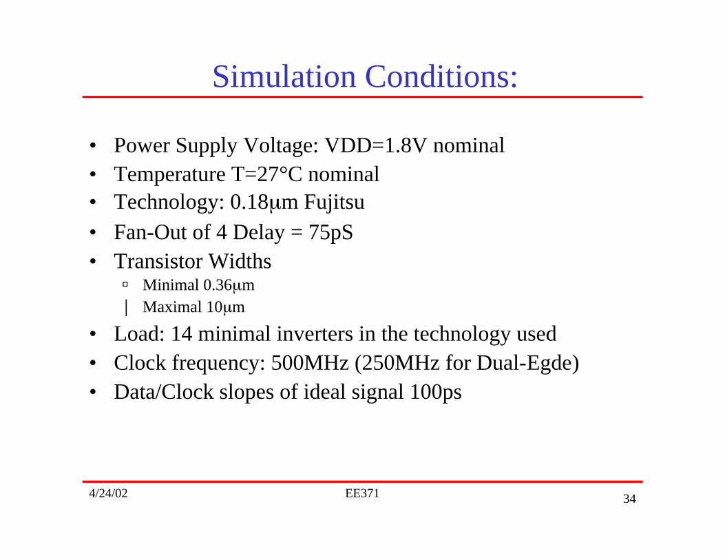
Simulation Conditions:
• Power Supply Voltage: VDD=1.8V nominal• Temperature T=27°C nominal• Technology: 0.18µm Fujitsu• Fan-Out of 4 Delay = 75pS• Transistor Widths
Minimal 0.36µm Maximal 10µm
• Load: 14 minimal inverters in the technology used• Clock frequency: 500MHz (250MHz for Dual-Egde)• Data/Clock slopes of ideal signal 100ps