
Lecture 7Lecture 7 Thin Film PV - Georgia Institute of...
21
Lecture 7 Lecture 7 Thin Film PV The Reading assignment for this lecture is: Armin G. Aberle, “Thin-Film solar cells”, Thin Solid Films, 517 (2009), pp4706-4710 Lawrence Kasmerski, J. Electron Spectroscopy And Related Phenomena, V. 150 (2006), pp. 105-135 Several images are from these references ECE 4833 - Dr. Alan Doolittle Georgia Tech
Transcript of Lecture 7Lecture 7 Thin Film PV - Georgia Institute of...

Lecture 7Lecture 7
Thin Film PV
The Reading assignment for this lecture is:
Armin G. Aberle, “Thin-Film solar cells”, Thin Solid Films, 517 (2009), pp4706-4710
Lawrence Kasmerski, J. Electron Spectroscopy And Related Phenomena, V. 150 (2006), pp. 105-135
Several images are from these references
ECE 4833 - Dr. Alan DoolittleGeorgia Tech

Thin Film Amorphous Si (a-Si:H) Solar Cells
Hydrogenated Amorphous Silicon is a dominate low-cost PV technology more yd oge a ed o p ous S co s a do a e ow cos V ec o ogy o eknown for its low cost than performance.
Advantages:Deposition is typically on inexpensive glass at low temperature (<200 degrees C)Relatively high absorption results in the need for very little material (<300nm)
ll ffi i i hi h h b dSmall area efficiencies as high as 9.5% have been reportedModule interconnects can be integrated making module costs very low.
Disadvantages:Disadvantages:Low (stable) efficiencies (<6%) limit use to primarily cheap consumer electronicsStaebler-Wronski effect (light induced degradation of the material) is aStaebler Wronski effect (light induced degradation of the material) is a primary efficiency limitationRequires a transparent conductive oxide layer (hurts transmission and series resistance)
ECE 4833 - Dr. Alan DoolittleGeorgia Tech
)

Why “Thin” Silicon
From Kasmerski 2005: Significant amounts of energy and costs go into
ECE 4833 - Dr. Alan DoolittleGeorgia Tech
From Kasmerski – 2005: Significant amounts of energy and costs go into making the silicon in a solar cell. If one can lower these costs, solar power can be made significantly cheaper. This does come at a performance penalty.

Why “Thin” Silicon:
Advantages in scale of Integrated Module Based Interconnect
ECE 4833 - Dr. Alan DoolittleGeorgia Tech
From Kasmerski – 2005: Since the module can be made monolithically, enormous advantages in scalability exist compared to “piece together” assembled modules.

History of Thin Silicon
From Kasmerski – 2005: Combinations of a-Si:H and C Si have shown significant improvement in recent yearsimprovement in recent years including modules that are above the magic 10% threshold.
ECE 4833 - Dr. Alan DoolittleGeorgia Tech

History of Thin Silicon
From Kasmerski – 2005: Examples of Single junctions and double junction tandems. Most thin films require a transparent semiconductor layer most often implemented as Indium Tin Oxide (ITO) or Zi O id (Z O) A i d h l d i l
ECE 4833 - Dr. Alan DoolittleGeorgia Tech
Zinc Oxide (ZnO). As a semiconductor, these layers are not as conductive as metals and have some minor absorption losses and thus, hurt performance.

Thin Film Amorphous Si (a-Si:H) Solar Cells
Hydrogenated Amorphous yd oge a ed o p ousSilicon is almost always produced by plasma deposition methods (PECVD – plasma enhanced chemical vapor deposition)
l b dPECVD can also be used to deposit anti-reflection coatings that simultaneously hydrogenate other materialshydrogenate other materials (c-Si).
ECE 4833 - Dr. Alan DoolittleGeorgia Tech
Plasmas
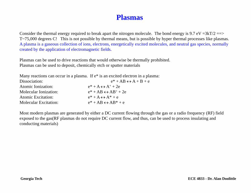
Consider the thermal energy required to break apart the nitrogen molecule. The bond energy is 9.7 eV =3kT/2 ==> gy q p g gyT~75,000 degrees C! This is not possible by thermal means, but is possible by hyper thermal processes like plasmas. A plasma is a gaseous collection of ions, electrons, energetically excited molecules, and neutral gas species, normally created by the application of electromagnetic fields.
Plasmas can be used to drive reactions that would otherwise be thermally prohibitedPlasmas can be used to drive reactions that would otherwise be thermally prohibited.Plasmas can be used to deposit, chemically etch or sputter materials
Many reactions can occur in a plasma. If e* is an excited electron in a plasma:Dissociation: e* + AB A + B + eAtomic Ionization: e* + A A+ + 2eMolecular Ionization: e* + AB AB+ + 2eAtomic Excitation: e* + A A* + eMolecular Excitation: e* + AB AB* + e
Most modern plasmas are generated by either a DC current flowing through the gas or a radio frequency (RF) field exposed to the gas(RF plasmas do not require DC current flow, and thus, can be used to process insulating and conducting materials)
ECE 4833 - Dr. Alan DoolittleGeorgia Tech
Parallel Plate SystemsAd Ch
Types of Plasma Systems
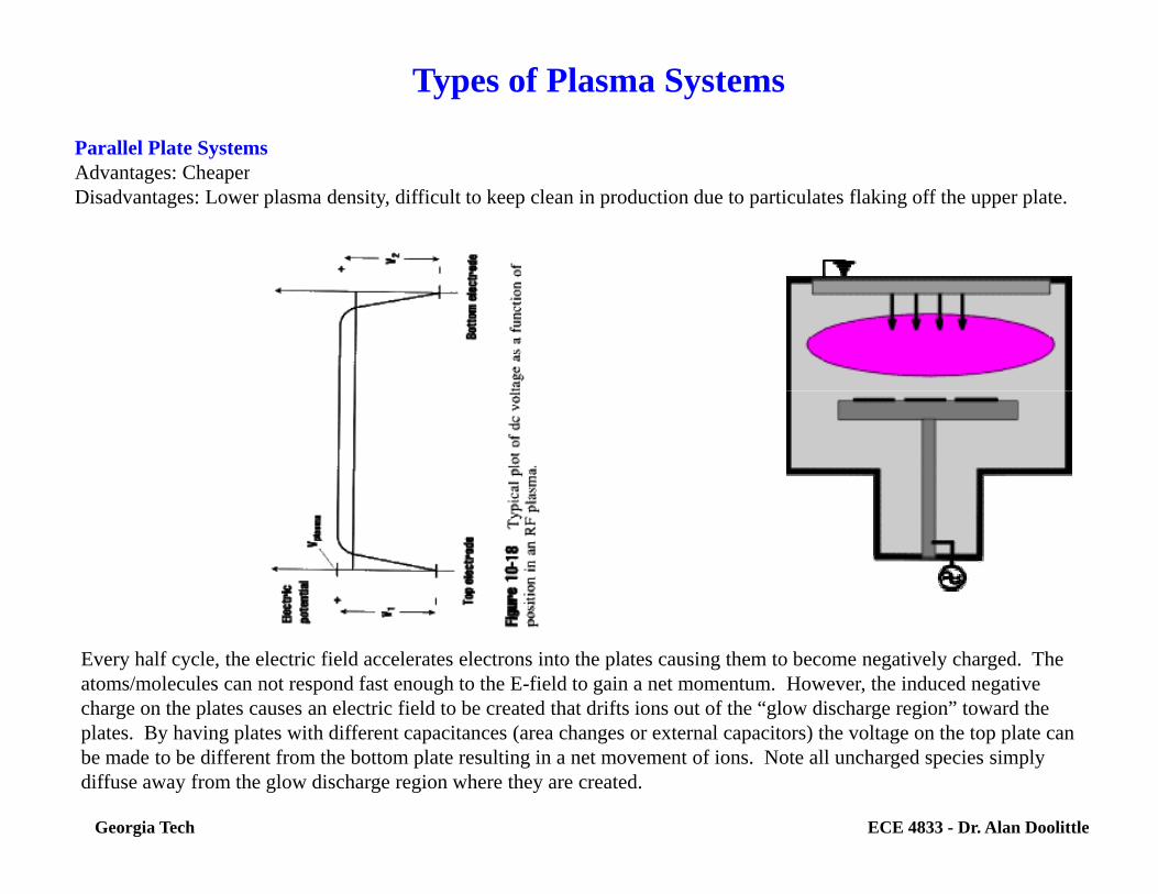
Advantages: CheaperDisadvantages: Lower plasma density, difficult to keep clean in production due to particulates flaking off the upper plate.
Every half cycle, the electric field accelerates electrons into the plates causing them to become negatively charged. The atoms/molecules can not respond fast enough to the E-field to gain a net momentum. However, the induced negative charge on the plates causes an electric field to be created that drifts ions out of the “glow discharge region” toward the
l t B h i l t ith diff t it ( h t l it ) th lt th t l t
ECE 4833 - Dr. Alan DoolittleGeorgia Tech
plates. By having plates with different capacitances (area changes or external capacitors) the voltage on the top plate can be made to be different from the bottom plate resulting in a net movement of ions. Note all uncharged species simply diffuse away from the glow discharge region where they are created.

Types of Plasma Systems
Inductively Coupled SystemsAd i h l d i ( 10 0 ) i l (l i l ) b if i lAdvantages: Higher plasma density (~10-50 x), easier to clean (low particulate), better uniformity over large areas. Disadvantages: Nearly 3 time the cost of a comparable parallel plate system.
Optional Magnets
Electromagnetic fields are induced into the gas by one or more coils located on the periphery of the vacuum chamber. Magnets may be used to enhance confinement of the plasma and control recombination (ions and electrons annihilatingMagnets may be used to enhance confinement of the plasma and control recombination (ions and electrons annihilating each other) at the chamber walls.
ECE 4833 - Dr. Alan DoolittleGeorgia Tech

Other Details of Plasma Systems
•The glow region contains many electrons and thus is highly•The glow region contains many electrons, and thus is highly conducting.==> Resistor Model element•The Sheaths have had their electrons stripped via the induced electric field. Thus, only limited ionic conduction occurs, along with a “depletion region capacitance” (this region is depleted of electrons).•The above lumped model results.•Note the frequency dependence of the plasma impedance.
ECE 4833 - Dr. Alan DoolittleGeorgia Tech

Other Details of Plasma SystemsNote also that at low frequencies, the ions are accelerated to higher energies (longer times) before the field reverses, resulting in higher energy ions bombarding the surface.g g gy g
ECE 4833 - Dr. Alan DoolittleGeorgia Tech

Thin Film II-VI Solar Cells
•Concerns over Cadmium contamination.
•Real but perhaps over blown. M d l li•Module recycling programs
exist.
Sources and Relative Contributions of Cadmium Exposure to Humans (in Europe)
Phosphate fertilizers 41.3 %p %Fossil fuel combustion 22.0 %
Iron and steel production 16.7 %Natural sources 8.0 %Natural sources 8.0 %
Non-ferrous metals 6.3 %Cement production 2.5 %
Cadmium products 2.5 %
ECE 4833 - Dr. Alan DoolittleGeorgia Tech
Cadmium products 2.5 %Incineration 1.0 %

Thin Film II-VI Solar Cells
Many cheap methods of production:Many cheap methods of production:•Physical deposition:•Sputtering, evaporation•Spray pyrolysis•Screen printing•Electro depositionp
CdCl2: Methanol anneal treatment lowers surface energy between grains promoting the fusing of grains togetherbetween grains, promoting the fusing of grains together promoting grain growth.
Uses p- I- n structure.
Cell efficiencies ~ 16.5%
ECE 4833 - Dr. Alan DoolittleGeorgia Tech
Modules ~11%

Thin Film II-VI Solar Cells
M i i i•Many variations exist.•Many companies have come and gone.
•First Solar with significant investment from the “Walmart” owners is currently the second largest PVthe second largest PV company in the world and is arguably the cheapest PV source in the world (claims of less than $1/watt).
ECE 4833 - Dr. Alan DoolittleGeorgia Tech
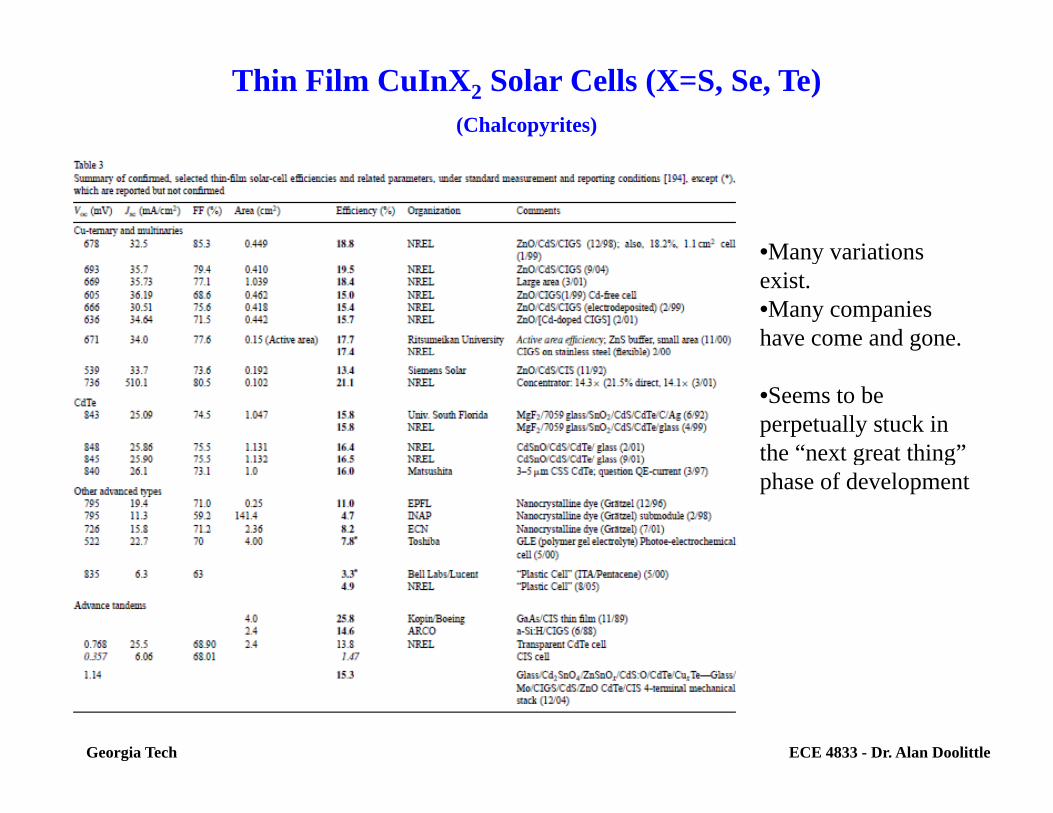
Thin Film CuInX2 Solar Cells (X=S, Se, Te)(Chalcopyrites)
•Many variations•Many variations exist.•Many companies have come and gone.
•Seems to be perpetually stuck in the “next great thing”the next great thing phase of development
ECE 4833 - Dr. Alan DoolittleGeorgia Tech

Thin Film CuInX2 Solar Cells
•Produced by elemental deposition (scaled up versions of MBE) . These have highest efficiencies.•Sputtering of metals then annealing in H2Se or Se vapor•Chemical deposition•ElectrochemicallyElectrochemically
ECE 4833 - Dr. Alan DoolittleGeorgia Tech

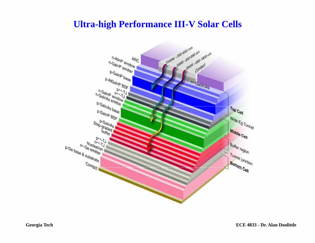
Ultra-high Performance III-V Solar Cells
See Giovanni Flamand /IMEC lecture (copyrighted so used in entirety).
ECE 4833 - Dr. Alan DoolittleGeorgia Tech
Ultra-high Performance III-V Solar Cells
ECE 4833 - Dr. Alan DoolittleGeorgia Tech

Ultra-high Performance III-V Solar Cells
ECE 4833 - Dr. Alan DoolittleGeorgia Tech

Ultra-high Performance III-V Solar Cells
See the additional III-V concentrator PV presentation from IMEC also on the lecture webpage. The topics and approaches currently being used are all covered in this lecture.lecture.
ECE 4833 - Dr. Alan DoolittleGeorgia Tech