Lecture 7 Work Function; Electron Emissionlgonchar/courses/p9826/Lecture7_Workfunction… ·...
16
Lecture 7 1 Lecture 7 Work Function; Electron Emission References: 1) Zangwill, p.57-63 2) Woodruff & Delchar, pp. 410-422, 461-484 3) Luth, pp.336, 437-443, 464-471 4) A. Modinos, “Field, Thermionic and Secondary Electron Spectroscopy”, Plenum, NY 1984. Outline: 1. Work Function 2. Electron Emission A. Thermionic Emission B. Field Emission C. Secondary Electron Emission 3. Measurements of Work Function
Transcript of Lecture 7 Work Function; Electron Emissionlgonchar/courses/p9826/Lecture7_Workfunction… ·...

Lecture 7 1
Lecture 7
Work Function; Electron Emission
References:1) Zangwill, p.57-63
2) Woodruff & Delchar, pp. 410-422, 461-484
3) Luth, pp.336, 437-443, 464-4714) A. Modinos, “Field, Thermionic and Secondary Electron Spectroscopy”,
Plenum, NY 1984.
Outline:
1. Work Function
2. Electron Emission
A. Thermionic Emission
B. Field EmissionC. Secondary Electron Emission
3. Measurements of Work Function

Lecture 7 2
• The “true work function” of a uniform surface of an electronic conductor is defined as the difference between the electrochemical potential of the electrons just inside the conductor, and the electrostatic potential energy of an electron in the vacuum just outside
• is work required to bring an electron isothermally from infinity to solid
• Note: is function of internal AND surface/external (e.g., shifting charges, dipoles) conditions;
• We can define quantity µ which is function of internal state of the solid
7.1 Work Function: Uniform Surfaces
φe
µ( )oeΦ−
µ
µ
Ene
rgy
distance
oeΦ−µ
φe
µIeΦ− (5.3)
(5.2)
(5.1) ,
e
ee
n
G
o
o
PTe
µφ
µφ
µ
−Φ−=
−Φ−=
∂∂=
IeΦ+= µµ Average electrostatic potential insideChemical potential of electrons:

Lecture 7 3
Work Function
• The Fermi energy [EF], the highest filled orbital in a conductor at T=0K, is measured with respect to and is equivalent to µ.
• We can write:
• ∆Φ depends on surface structure and adsorbed layers. The variation in φ for a solid is contained in ∆Φ.
• What do we mean by potential just outside the surface???
( )IeΦ−
(5.5)
(5.4)
e
eee Io
µφ
µφ
−∆Φ=
−Φ+Φ−=

Lecture 7 4
Potential just outside the surface
The potential experienced by an electron just outside a conductor is:
For a uniform surface this corresponds to Φo in (5.1):
In many applications, an accelerating field, F, is applied:
(5.6) 1099.8164
)(2
9
C
Nme
r
ekrV
o
e ×=−=−=πε
]10for range mV[in r as 0)( 3 ÅrrV ≥∞→→
( )mVÅmrF
FFeFk
mFF
ekr
dr
dVr
ekFrrV
o
e
eo
rr
e
8.3 1900109.1 V/cm), (100 Volts/m10For
(5.9) Volts/m)in ( Volts 1079.3
(5.8) 109.11
4
0
(5.7) 4
)(
74
2/152/1
2/1
5
2/1
2/1
0
==×==
×==
×=
=
=
−−=
−
−
−
=
δφδφ2/1F∝δφ

Lecture 7 5
Selected Values of Electron Workfunctions*
Units: eV electron Volts; *Reference: CRC handbook on Chemistry and Physics version 2008, p. 12-114.
4.05Zr4.60Mo2.14Cs
4.55W2.66LaB64.5Cr
4.53Ti2.30K2.9Ce
4.00Ta (111)5.76Ir(111)5.0C
4.80Ta (110)5.42Ir (110)2.52Ba
4.15Ta (100)4.98Cu(111)4.74Ag (111)
4.25Ta4.48Cu(110)4.52Ag (110)
4.71Ru4.59Cu(100)4.64Ag (100)
4.85Si4.65Cu4.26Ag
φ (eV)Elementφ (eV)Elementφ (eV)Element

Lecture 7 6
Work Function: Polycrystalline Surfaces
Consider polycrystalline surface with “patches” of different workfunction, and different value of surface potential
At small distance ro above ith patch electrostatic potential is Φoi
At distances large w/r/t/ patch dimension:
So mean work function is given by:
- at low applied field, electron emission controlled by:
- at high field (applied field >> patch field)electron emission related to individual patches:
On real surfaces, patch dimension < 100Å, if ∆φ~ 2 eV then patch field F ~ 2V/(10-6 cm ) ~ 2 x 10⁶ Volts/cm. work required to bring an electron from infinity to solid
pomm
lkj, …i, Φoi
patch i of area fractional , thff ii
oiio =Φ=Φ ∑
(5.10) ∑=i
iiefe φφ
φe
ieφ

Lecture 7 7
Workfunction
Factors that influence work function differences on clean surfaces:
• Adsorbed layers
• Surface dipoles (cf. Zangwill, p 57)• Smooth surface: electron density “spillover”
• Electron density outside rough surface• For tungsten
(110)5.70
(116)4.30
(111)4.39
(211)4.93
W planeeφ, eV
Lecture 7 8
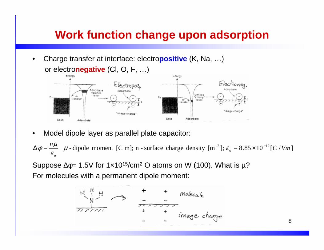
Work function change upon adsorption
• Charge transfer at interface: electropositive (K, Na, …)
or electronegative (Cl, O, F, …)
• Model dipole layer as parallel plate capacitor:
Suppose ∆φ= 1.5V for 1×10¹⁵/cm2 O atoms on W (100). What is µ?For molecules with a permanent dipole moment:
]/[1085.8 ];[mdensity charge surface -n m]; [Cmoment dipole- 12o
2- VmCn
o
−×==∆ εµεµφ

Lecture 7 9
7.2.1Electron Sources: Thermionic Emission
• Richardson’s Equation : (derivation – aside)
Current density, j:
r = reflection coefficient;
• Richardson plot :
ln(j/T2) vs 1/T ⇒
⇒ straight line
)exp()1( 2
kT
eTrAj o
φ−−=
223
2
deg4.120
4
cm
Amp
h
mekAo == π
Thermionic emission occurs when sufficient heat is supplied to the emitter so that e’s can overcome the work function, the energy barrier of the filament, Ew, and escape from it

Lecture 7 10
7.2.1 Electron Emission: Thermionic Emission
• Richardson plot :
ln(j/T2) vs 1/T ⇒
⇒ straight line
• Schottky Plot
linestraight vsln
eq.5.9) (cf. 2/1
2/1
⇒
−Φ→
Fj
bFee oφ

Lecture 7 11
7.2.2 Field Electron Emission
• Electron tunneling through low, thin barrier
– Field emission, when F>3×10⁷ V/cm ~ 0.3 V/Å• General relation for electron emission in high field:
• P is given by WKB approximation
• If approximate barrier by triangle:
• Fowler – Nordheim eqn, including potential barrier:
ZZZ dEEvFEPej )(),(0∫∞
=
−−×= ∫
l
Z dzEVm
constP0
2/12/13/2
)(2
exph
FF
2/32/1
2
1~
2
1~
φφφ∫
−×=
F
mconstP
2/32/13/22exp
φh
φφ
φ
2/12/32/372
26 where;
)(1083.6exp)(1054.1
Fey
F
yfyt
Fj =
×−×= −
Lecture 7 12
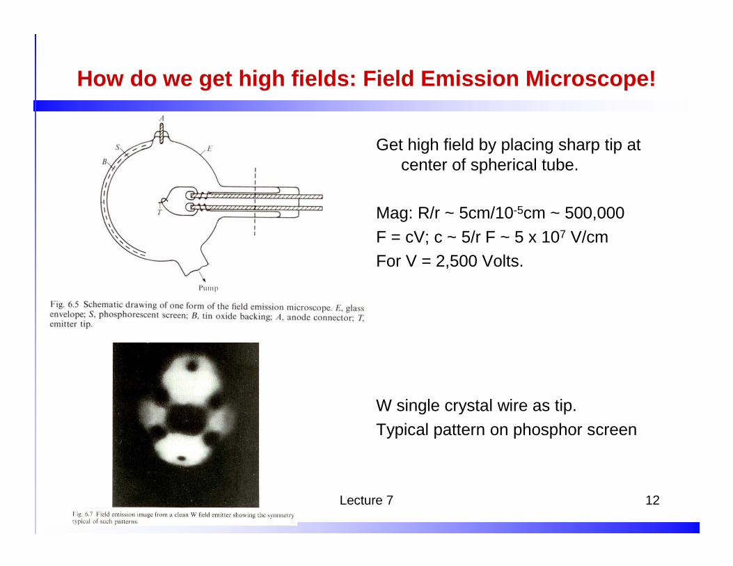
How do we get high fields: Field Emission Microscop e!
Get high field by placing sharp tip at center of spherical tube.
Mag: R/r ~ 5cm/10-5cm ~ 500,000
F = cV; c ~ 5/r F ~ 5 x 10⁷ V/cmFor V = 2,500 Volts.
W single crystal wire as tip.
Typical pattern on phosphor screen

Lecture 7 13
Field Emission Properties
Lecture 7 14
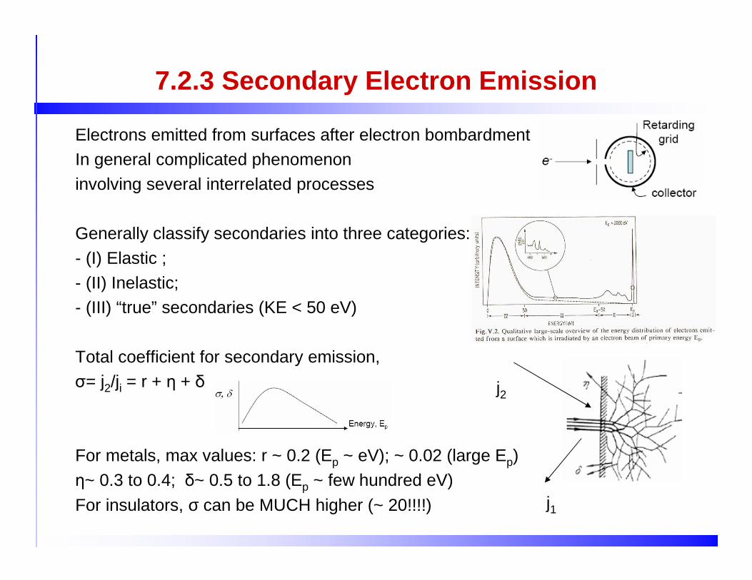
7.2.3 Secondary Electron Emission
Electrons emitted from surfaces after electron bombardmentIn general complicated phenomenon
involving several interrelated processes
Generally classify secondaries into three categories:
- (I) Elastic ;
- (II) Inelastic;- (III) “true” secondaries (KE < 50 eV)
Total coefficient for secondary emission,σ= j2/ji = r + η + δ
For metals, max values: r ~ 0.2 (Ep ~ eV); ~ 0.02 (large Ep)
η~ 0.3 to 0.4; δ~ 0.5 to 1.8 (Ep ~ few hundred eV)
For insulators, σ can be MUCH higher (~ 20!!!!)
j2
j1

Lecture 7 15
Secondary Electron Emission
• Establishment of stable potential for insulators and dielectric materials
• For metals and semiconductors: Correlation between δ and density, ρ
In practice, steady state potential reached by dielectic is due mainly to incomplete extraction of secondary electrons

Lecture 7 16
7.3 Measurements of Workfunction
Absolute value of φφφφA. Photoemission
W = full width of energy distribution
B. Thermionic Emission (Richardson’s Equation)
C. Field Emission Retarding Potential (FERP)
Workfunction differenceA. Shelton Method
B. Vibrating Capacitor – Kelvin Probe
http://www.kelvinprobe.info/
Wh −= νφ


![Lecture 7 Work Function; Electron Emissionlgonchar/courses/p9826/... · Lecture 7 3 Work Function • The Fermi energy [E F], the highest filled orbital in a conductor at T=0K, is](https://static.fdocuments.in/doc/165x107/60dc943e94138518b4706cd5/lecture-7-work-function-electron-emission-lgoncharcoursesp9826-lecture.jpg)