
Lecture 6: Digital/Analog Techniques - University of · PDF fileLecture 6: Digital/Analog...
21
Lecture 6: Digital/Analog Techniques • The electronics signals that we’ve looked at so far have been analog – that means the information is continuous. A voltage of 5.3V represents different information that a voltage of 5.4V • For most of the remainder of the semester, we’ll investigate the processing of digital information • In digital electronics, we define a range of voltages called “low” and another range called “high” – For example, 0-2V may be low, and 5-10V may be high • The information carried is either a 0 (voltage in low range) or 1 (voltage in high range) – circuits are built so that voltages in the middle are not possible – if such a voltage is observed, it means something is broken!
-
Upload
duongxuyen -
Category
Documents
-
view
218 -
download
2
Transcript of Lecture 6: Digital/Analog Techniques - University of · PDF fileLecture 6: Digital/Analog...

Lecture 6: Digital/Analog Techniques• The electronics signals that we’ve looked at so far have been
analog– that means the information is continuous. A voltage of 5.3V
represents different information that a voltage of 5.4V
• For most of the remainder of the semester, we’ ll investigate theprocessing of digital information
• In digital electronics, we define a range of voltages called “ low” and another range called “high”– For example, 0-2V may be low, and 5-10V may be high
• The information carried is either a 0 (voltage in low range) or 1 (voltage in high range)– circuits are built so that voltages in the middle are not possible – if
such a voltage is observed, it means something is broken!

Advantages to Digital• It seems that we lose a lot of information in going from
analog to digital processing• But more and more real signal processing is digital,
because:– noise is much less of a concern. A small noise voltage on
top of the signal can distort analog information, but has no effect digitally
– digital information is easier to store. One could design a system of capacitors to retain a fixed analog charge, but even small leakage would result in the information being lost over time
– digital information can easily be processed in logical operations like AND and OR. These operations are at the heart of all computers
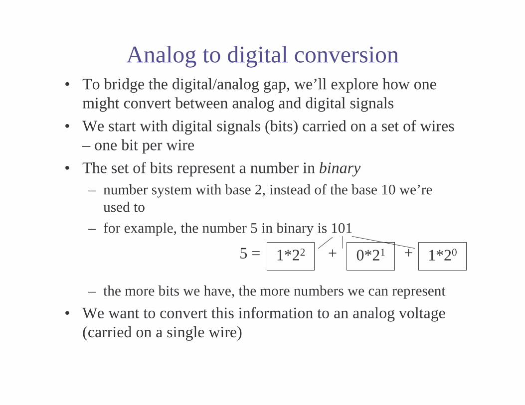
Analog to digital conversion• To bridge the digital/analog gap, we’ ll explore how one
might convert between analog and digital signals
• We start with digital signals (bits) carried on a set of wires – one bit per wire
• The set of bits represent a number in binary– number system with base 2, instead of the base 10 we’ re
used to
– for example, the number 5 in binary is 101
– the more bits we have, the more numbers we can represent
• We want to convert this information to an analog voltage (carried on a single wire)
1*200*211*22 + +5 =

• One way to make a digital-to-analog converter (DAC) is the following:
• The digital input determines which of the four switches is closed– low bit means switch is open
– with all four switches open, Vout is 0
Most significant bit
(MSB)
Least significant bit (LSB)

• Let’s see what happens as we close other switches:
• If we close the LSB switch, we find (using ideal op-amp rules):
this is the smallest voltage increment possible for this DAC
• Closing the MSB switch gives:
0 82
8 2 16
out
out
RV V IR V I
V R VV
R
− = = − = −
= =
02
2 2
out
out
RV V IR V I
V R VV
R
− = = − = −
= =
8 times bigger than LSB value

• Now we’ ll close all four switches:
• The resistance between +V and V- is:
• Which means the output voltage is:
which is 15 times the LSB value
1 1 2 4 8 15
15
T
T
R R R R R R
RR
= + + + =
=
015 2
15 15
2 2
out
out
R RV V I V I
V R VV
R
− = = − = −
= =

• While that circuit will work in principle, it’ s not really practical– to keep current draw low, R can’ t be too small – let’s say we
make it 10kΩ– if we want a 10-bit DAC, the biggest resistor would then be
29 x 10kΩ, which is 5MΩ• hard to put that kind of resistance on an IC
• There’s also a problem due to “stray capacitance”– that means that adjacent wires can act as small capacitors
– for this circuit, the total stray capacitance might be ~100pF
– that means that the time it takes for the output to reach its desired value after the switches are closed is
– that might seem pretty quick to you and me, but to a computer it would be painfully slow
45M 100pF 5 10 st RC −= = Ω ⋅ = ×

A better DAC• Let’s try this design instead:
• Note that V- is a “virtual ground”– that is, its voltage is nearly 0
• Hence moving the switches does not change the total current flowing from VCC
– but it does change the current flowing through the feedback resistor
MSB
LSB
IR
I1I2I3I4
I0ABCD

• The output voltage is:
• Looking at the ladder from point A, the equivalent resistance to ground is:
• Meaning we could redraw the ladder as:
0 out R
out R
V v I R
v I R− = = −
=
1 1 1
2 2T
T
R R R
R R
= +
=

• Looking at this “equivalent ladder” from point B, we see the same resistance to ground as the original ladder had from point A. So we could draw a new equivalent ladder as:
• At this point, we see the pattern will keep repeating– thus the total resistance of the ladder is R
– this is true no matter how long the ladder is
• The total current flowing from VCC is VCC/R

• What about the individual currents I1 through I4?
• Look at the ladder from point D– there are two paths through ground:
1. Through a single resistor 2R (this is where I1 flows)
2. Through a resistor R, and then the ladder at point C– but we already know that all ladders have resistance R
– so the total resistance for this path is also 2R
– this means the current splits up evenly at point D, so:
• Similarly, even current splits occur at points C, B, and A, so:
4
1
2 2CC
T
VI I
R= =
3 2 1; ; 4 8 16
CC CC CCV V VI I I
R R R= = =

• Now let’s switch the LSB so it’s connected to V-
– the total current flowing toward V- is then I1 = VCC/16R
– which means vout is VCC/16
• If instead the MSB switch is connected to V-, we have
• So we see this circuit does in fact act as a DAC
• Advantages:– only two resistor values needed
– resistance can be modest (no matter how many bits are to be converted)
– settling time is therefore much faster
4 2CC
out
Vv I R= =

Analog-to-Digital Converters (ADCs)• We sometimes also want to go in the other direction, and
convert an analog voltage to a set of bits– used all the time in physics experiments
– for example, to convert analog information about the ionization from a charged particle into digital form for storage and processing on a computer
• We’ve already seen one such circuit – the comparator– this converts an analog voltage into one bit of information
• But what if we want more bits?

• That’s easy! We’ ll just use a lot of comparators:
• Each op-amp compares Vin to V+

• The V+ values at each op-amp input are the result of the voltage divider from VCC
– i.e., the op-amp on bottom sees a voltage of VCC/8, while the one on top sees 7VCC/8
• Note that there are only 8 possible outputs from the comparators– this is a 3-bit ADC
• Additional processing is required to convert the eight output lines from the comparators to a binary number– that’s what the chip on the right side of the schematic does
– it’ s called a “priority encoder”

• The main advantage of this design is that it’s fast– result of voltage comparisons can propagate through op-
amps and priority encoder in a few ns
• The drawbacks are:– you need a lot of comparators (256 for an 8-bit DAC, 65,536
for a 16-bit DAC!)
– accuracy is limited by tolerance of resistors

Ramp DAC
• Parts of this are familiar– the comparator and active integrator
• Other parts are digital devices we haven’ t seen before– the AND gate’s output is 1 if both inputs are 1, and 0
otherwise
– we’ ll talk about this more next week
AND gate

• The “clock” is just a square wave generator– output periodically switches between 0 and 1
• The counter’s output is a binary number equal to the number of times the input has been 1 since the last time the counter was reset
• The circuit works as follows– signal is sent to discharge capacitor and reset clock
(capacitor discharged though FET switch)– input to comparator (vc) is integral of Vref
• in other words, a linearly increasing voltage
– as long a vin > vc, comparator output is 1– thus, output of AND gate is 1 whenever the clock is 1– once vin < vc, the comparator outputs 0– counter stops incrementing!
• The couter output is vin in binary

• This ADC is more precise and simpler than the one using many comparators
• However, it’s slower (have to wait for voltage to integrate)
• An even better solution is the “dual slope ramp” ADC
• The only difference is that the inputs are rearranged:

• In this case, when one starts the conversion the switch is set to the unknown vin
• This is then integrated for a fixed number of clock cycles– usually a multiple of the AC power period
• Then the switch is set to –vref, and the counter is told to start counting– capacitor then starts discharging
– when voltage across capacitor falls to 0, comparator output goes to 0, and counter stops
• As before, the value stored in the counter is now proportional to vin

• This ADC is more precise than the single-ramp one because:– same clock is used for both charging and discharging the
capacitor – so if the frequency drifts slowly over time, we don’ t care
– similarly, if the capacitor degrades slowly, that won’ t affect the output
– noise coming from the power line is averaged out in the initial integration


