Lecture 4 - solidification 4 - solidification.pdf · Solidification of Metals ... Energies involved...
125
CHAPTER 4 Solidification and Crystalline Imperfections in Solids 4-1
Transcript of Lecture 4 - solidification 4 - solidification.pdf · Solidification of Metals ... Energies involved...
CHAPTER
4Solidification
and Crystalline Imperfections
in Solids4-1

Solidification of Metals
• Metals are melted to produce finished and semi-finished parts.
• Two steps of solidification Nucleation : Formation of stable nuclei. Growth of nuclei : Formation of grain structure.
• Thermal gradients define the shape of each grain.
Liquid
Nuclei
Crystals that willForm grains
Grain Boundaries
Grains
4-2Figure 4.2

Formation of Stable Nuclei
• Two main mechanisms: Homogenous and heterogeneous.
• Homogenous Nucleation :First and simplest case.Metal itself will provide atoms to form nuclei.Metal, when significantly undercooled, has several slow moving atoms which bond each other to form nuclei. Cluster of atoms below critical size is called embryo.If the cluster of atoms reach critical size, they grow into crystals. Else get dissolved.Cluster of atoms that are grater than critical size are
called nucleus.
4-3

Energies involved in homogenous nucleation.
Volume free energy Gv
• Released by liquid to solid transformation.
• ΔGv is change in free energy per unit volume between liquid and solid.
• free energy change for a spherical nucleus of radius r is given by
Surface energy Gs
• Required to form new solid surface
• ΔGs is energy needed to create a surface.
• γ is specific surface free energy.
Then
• ΔGs is retarding energy.
γπ 2s 4G r=Δ
γ
vGrr Δ= 3
34
π
4-4

Total Free Energy
• Total free energy is given by γππ 23 434
rGrG vT +Δ=Δ
Nucleus
Above criticalradius r*
Below criticalradius r*
Energy lowered by
growing intocrystals
EnergyLowered byredissolving
VGr
Δ−=
γ2*Since when r=r*, d(ΔGT)/dr = 0
r*r
ΔG
+
- ΔGv
ΔGs
ΔGT
4-4
r*
Figure 4.4


Critical Radius Versus Undercooling
• Greater the degree of undercooling, greater the change in volume free energy ΔGv
• ΔGs does not change significantly.• As the amount of undercooling ΔT increases, critical
nucleus size decreases.• Critical radius is related to undercooling by relation
THT
rf
m
ΔΔ=
γ2*
r* = critical radius of nucleusγ = Surface free energyΔHf = Latent heat of fusionΔ T = Amount of undercooling.
4-6

Heterogeneous Nucleation
• Nucleation occurs in a liquid on the surfaces of structural materials Eg:- Insoluble impurities.
• These structures, called nucleating agents, lower the free energy required to form stable nucleus.
• Nucleating agents also lower the critical size.• Smaller amount of undercooling is required to solidify.• Used excessively in industries.
Liquid
Solid
Nucleating agent
θ
4-7
Figure 4.6

Growth of Crystals and Formation of Grain Structure
• Nucleus grow into crystals in different orientations.• Crystal boundaries are formed when crystals join
together at complete solidification. • Crystals in solidified metals are called grains.• Grains are separated by grain boundaries.• More the number of
nucleation sites available, more the number of grains formed.
Nuclei growing into grainsForming grain boundaries
4-8
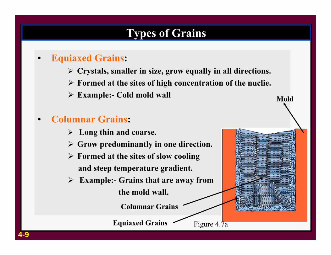
Types of Grains
• Equiaxed Grains: Crystals, smaller in size, grow equally in all directions.Formed at the sites of high concentration of the nuclie.Example:- Cold mold wall
• Columnar Grains: Long thin and coarse.Grow predominantly in one direction.Formed at the sites of slow coolingand steep temperature gradient.Example:- Grains that are away from
the mold wall.
Columnar Grains
Equiaxed Grains
Mold
4-9Figure 4.7a

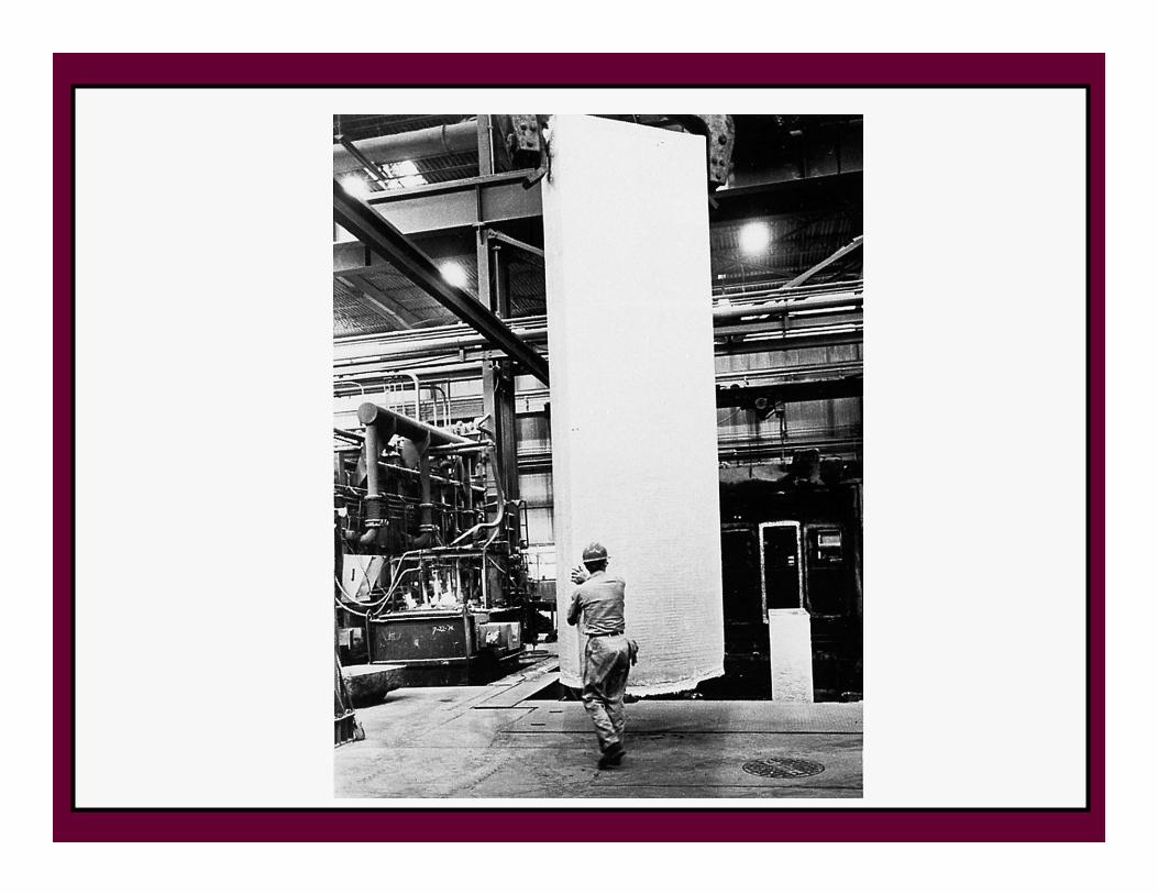
Casting in Industries
• In industries, molten metal is cast into either semi finished or finished parts.
4-10
Figure 4.8Direct-Chill semicontinuousCasting unit for aluminum
Figure 4.9b
Continuous castingOf steel ingots

Grain Structure in Industrial castings
• To produce cast ingots with fine grain size, grain refiners are added.
• Example:- For aluminum alloy, small amount of Titanium, Boron or Zirconium is added.
4-11Figure 4.10
(a) (b)
Grain structure ofAluminum cast with (a) and without (b)grain refiners.
After “Metals Handbook” vol. 8, 8th ed., American Society of Metals, 1973, p.164)

Solidification of Single Crystal
• For some applications (Eg: Gas turbine blades-high temperature environment), single crystals are needed.
• Single crystals have high temperature creep resistance. • Latent head of solidification is conducted through
solidifying crystal to grow single crystal.• Growth rate is kept slow so that temperature at solid-
liquid interface is slightly below melting point.
4-12
Figure 4.12
Growth of singlecrystal for turbineairfoil.
(After Pratt and Whitney Co.)

Czochralski Process
• This method is used to produce single crystal of silicon for electronic wafers.• A seed crystal is dipped in molten silicon and rotated.• The seed crystal is withdrawn slowly while silicon adheres to seed crystal and
grows as a single crystal.
4-13
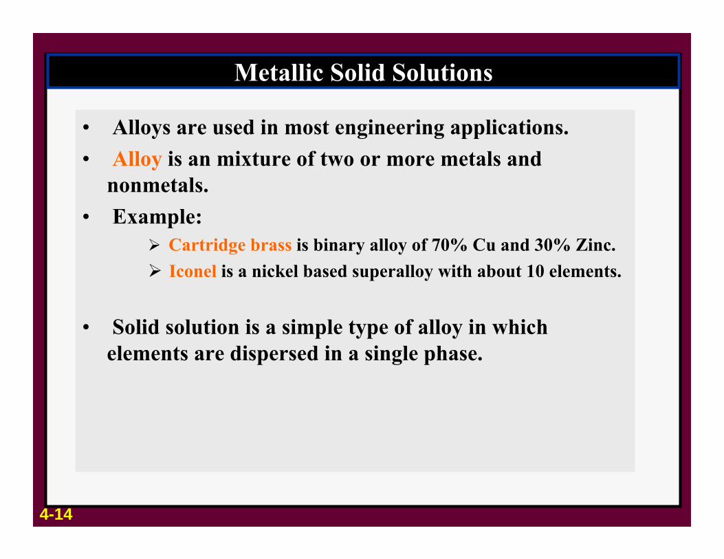
Metallic Solid Solutions
• Alloys are used in most engineering applications.• Alloy is an mixture of two or more metals and
nonmetals.• Example:
Cartridge brass is binary alloy of 70% Cu and 30% Zinc. Iconel is a nickel based superalloy with about 10 elements.
• Solid solution is a simple type of alloy in which elements are dispersed in a single phase.
4-14

Substitutional Solid Solution
• Solute atoms substitute for parent solvent atom in a crystal lattice.
• The structure remains unchanged.• Lattice might get slightly distorted due to change in
diameter of the atoms. • Solute percentage in solvent
can vary from fraction of a percentage to 100%
Solvent atoms
Solute atoms
4-15
Figure 4.14

Substitutional Solid Solution (Cont..)
• The solubility of solids is greater if The diameter of atoms not differ by more than 15% Crystal structures are similar. No much difference in electronegativity (else compounds
will be formed). Have some valence.
• Examples:-
100%02.3%Cu-Ni
0.17%0.236.7%Cu-Pb
38.3%0.13.9%Cu-Zn
SolidSolibility
Electron-egativity
difference
Atomic radius
DifferenceSystem
4-16

Interstitial Solid Solution
• Solute atoms fit in between the voids (interstices) of solvent atoms.
• Solvent atoms in this case should be much larger than solute atoms.
• Example:- between 912 and 13940C, interstitial solid solution of carbon in γ iron (FCC) is formed.
• A maximum of 2.8% of carbon can dissolve interstitially in iron.
Carbon atoms r=0.075nm
Iron atoms r00.129nm
4-17Figure 4.15a

Crystalline Imperfections
• No crystal is perfect.• Imperfections affect mechanical
properties, chemical properties and electrical properties.
• Imperfections can be classified as Zero dimension point defects.One dimension / line defects (dislocations). Two dimension defects.Three dimension defects (cracks).
4-18

Point Defects – Vacancy
• Vacancy is formed due to a missing atom.• Vacancy is formed (one in 10000 atoms)
during crystallization or mobility of atoms. • Energy of formation is 1 ev.• Mobility of vacancy results in cluster of
vacancies.• Also caused due
to plastic defor--mation, rapid cooling or particlebombardment.
Figure: Vacancies moving to form vacancy cluster
4-19
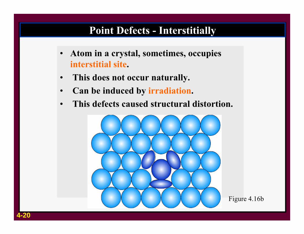
Point Defects - Interstitially
• Atom in a crystal, sometimes, occupies interstitial site.
• This does not occur naturally.• Can be induced by irradiation.• This defects caused structural distortion.
4-20
Figure 4.16b

Point Defects in Ionic Crystals
• Complex as electric neutrality has to be maintained.• If two appositely charged particles are missing, cation-
anion divacancy is created. This is Schottky imperfection.
• Frenkel imperfection is created when cation moves to interstitial site.
• Impurity atoms are also considered as point defects.
4-21Figure 4.17

Electric Conduction – Classical Model
• Metallic bonds make free movement of valence electrons possible.
• Outer valence electrons are completely free to move between positive ion cores.
• Positive ion cores vibrate with greater amplitude with increasing temperature.
• The motion of electrons are random and restricted in absence of electric field.
• In presence of electric field, electrons attain directed drift velocity.
14-2


• Valence electrons are delocalized, interact and interpenetrate each other.• Their sharp energy levels are broadened into energy bands.• Example:- Sodium has 1 valence electron (3S1). If there are N sodium atoms, there are N distinct 3S1 energy levels in 3S band.• Sodium is a good conductor since it has half filled outer orbital


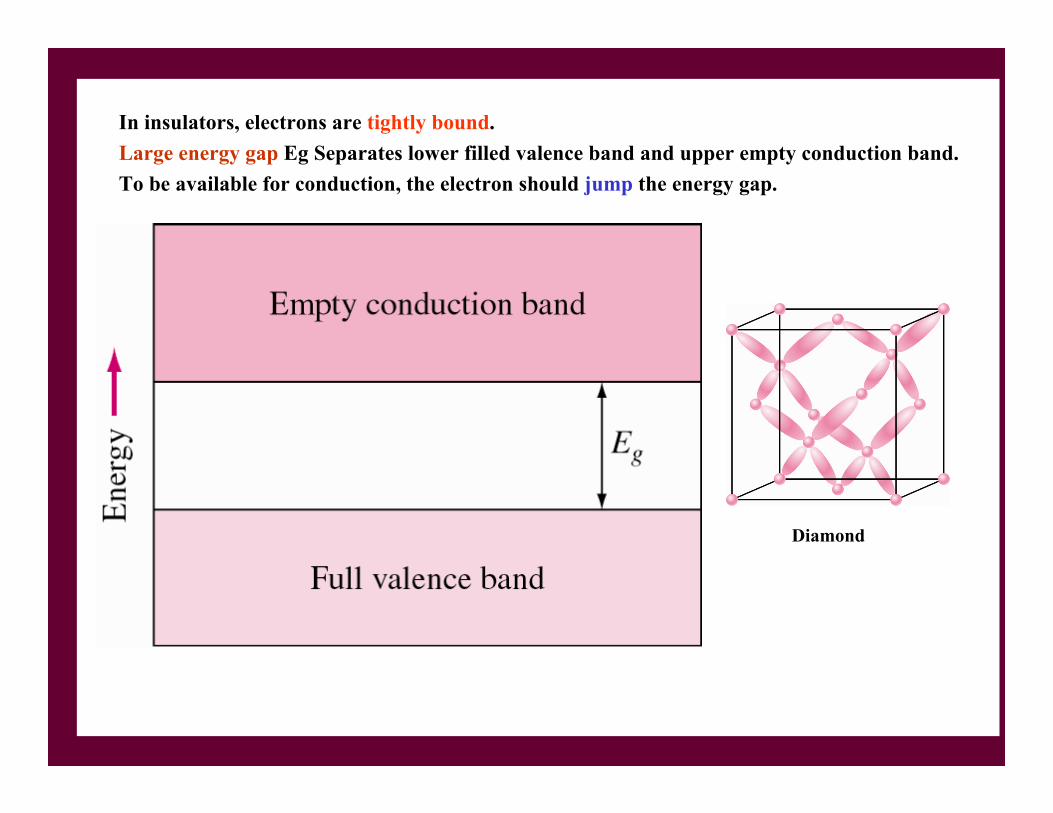
In insulators, electrons are tightly bound.Large energy gap Eg Separates lower filled valence band and upper empty conduction band.To be available for conduction, the electron should jump the energy gap.
Diamond

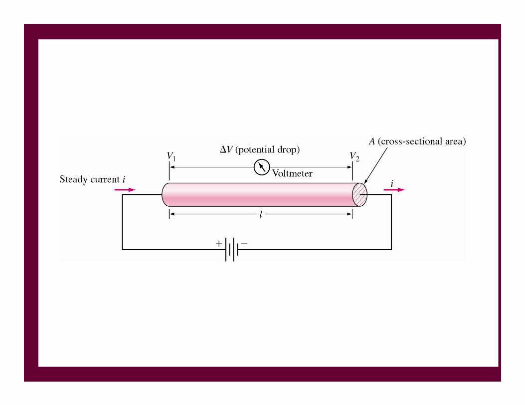
Ohm’s Law• Ohm’s law states that electric current flow I is directly proportional to the applied voltage V and inversely proportional to
resistance of the wire:
i = V/R where i = electric current (A)V = potential difference (V)R = resistance of wire (Ω)
• Electric resistivity ρ = RA/ll = length of the conductorA = cross-sectional area of the conductor
• Electric Conductivity σ = 1/ ρ
SiliconGermanium
PolyethylenePolystyrene
SilverCopper Gold
SemiconductorsInsulatorsConductors
14-3

Conduction in Intrinsic Semiconductors
• Semiconductors: Conductors between good conductors and insulators.• Intrinsic Semiconductors: Pure semiconductors and conductivity depends
on inherent properties.• Example: Silicon and Germanium – each atom contributes 4 valence
electrons for covalent bond.• Valence electrons are excited
away from their bondingposition when they are excited.
• Moved electron leaves a hole behind.
Figure 13.16
14-8

Electrical Charge Transport in Pure Silicon
• Both electrons and holes are charge carriers.• Hole is attracted to negative terminal, electron to the
positive terminal
Valence electron ‘A’ is missing – HoleValence electron ‘B’ moves to that spot due to the electric field
leaving behind a hole.Movement of electrons is opposite to the electric field.
Figure 13.18 Figure 13.19
14-9
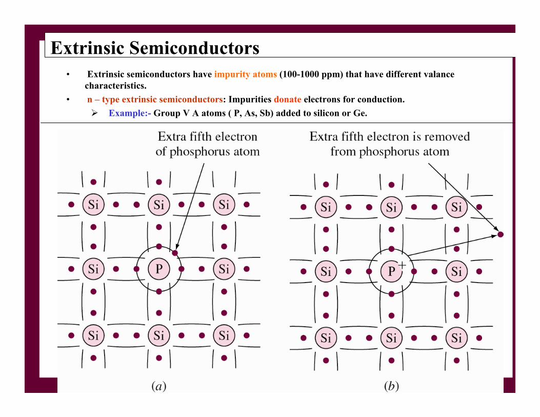
Extrinsic Semiconductors• Extrinsic semiconductors have impurity atoms (100-1000 ppm) that have different valance
characteristics.• n – type extrinsic semiconductors: Impurities donate electrons for conduction.
Example:- Group V A atoms ( P, As, Sb) added to silicon or Ge.

Extrinsic Semiconductors

P-Type Extrinsic Semiconductors
• Group III A atoms when added to silicon, a hole is created since one of the bonding electrons is missing
• When electric field is applied, electrons from the neighboring bond move to the hole
• Boron atom gets ionized and hole moves towards negative terminal
• B, Al, provide acceptor level energy and are hence called acceptor atoms
• Doping: Impurity atoms (dopants) are deposited into silicon by diffusion at 11000C.
14-13


Line Defects – (Dislocations)
• Lattice distortions are centered around a line.
• Formed duringSolidificationPermanent DeformationVacancy condensation
Atomic mismatch
• Different types of line defects areEdge dislocationScrew dislocation Mixed dislocation
4-22

Edge Dislocation
• Created by insertion of extra half planes of atoms.
• Positive edge dislocation
• Negative edge dislocation
• Burgers vectorShows displa-cement of atoms (slip).
4-23
Burgers vector
Figure 4.18
After A.G. Guy , “Essentials of Materials Science,” McGraw-Hill, 1976, p.153After M. Eisenstadt, “Introduction to Mechanical Properties of Materials,” Macmillan, 1971, p.117

Screw Dislocation
• Created due to shear stresses applied to regions of a perfect crystal separated by cutting plane.
• Distortion of lattice in form of a spiral ramp.• Burgers vector is parallel to dislocation line.
4-24 After M. Eisenstadt, “Introduction to Mechanical Properties of Materials,” Macmillan, 1971, p.118

Mixed Dislocation
• Most crystal have componentsof both edge and screw dislocation.
• Dislocation, since have irregular atomic arrangementwill appear as dark lineswhen observed in electronmicroscope.
4-25
Figure 4.21
(After John Wolff et al., “Structure and Properties of Materials,” vol 3: “Mechanical Properties,” Wiley, 1965, p.65.(After “Metals Handbook” vol. 8, 8th ed., American Society of Metals, 1973, p.164)
Figure 4.22Dislocation structure of iron deformed14% at –1950C

Planar Defects
• Grain boundaries, twins, low/high angle boundaries, twists and stacking faults
• Free surface is also a defect : Bonded to atoms on only one side and hence has higher state of energy Highly reactive
• Nanomaterials have small clusters of atoms and hence are highly reactive.
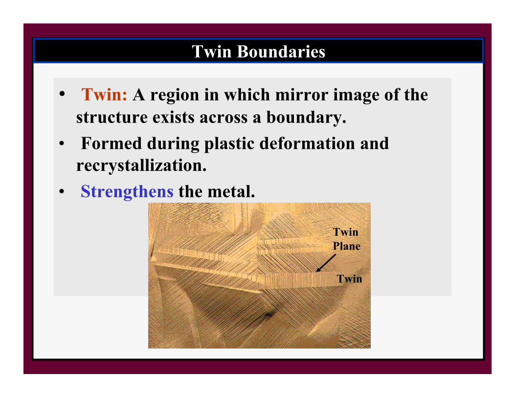
Twin Boundaries
• Twin: A region in which mirror image of the structure exists across a boundary.
• Formed during plastic deformation and recrystallization.
• Strengthens the metal.
Twin
Twin Plane

Other Planar Defects
• Small angle tilt boundary: Array of edge dislocations tilts two regions of a crystal by < 100
• Stacking faults: Piling up faults during recrystallization due to collapsing.
Example: ABCABAACBABC FCC fault
• Volume defects: Cluster of point defects join to form 3-D void.

Grain Size
• Affects the mechanical properties of the material
• The smaller the grain size, more are the grain boundaries.
• More grain boundaries means higher resistance to slip (plastic deformation occurs due to slip).
• More grains means more uniform the mechanical properties are.
4-30

Measuring Grain Size
• ASTM grain size number ‘n’ is a measure of grain size.N = 2 n-1 N = Number of grains per
square inch of a polishedand etched specimen at 100 x.n = ASTM grain size number.
200 X 200 X
1018 cold rolled steel, n=10 1045 cold rolled steel, n=84-31
N < 3 – Coarse grained4 < n < 6 – Medium grained7 < n < 9 – Fine grainedN > 10 – ultrafine grained
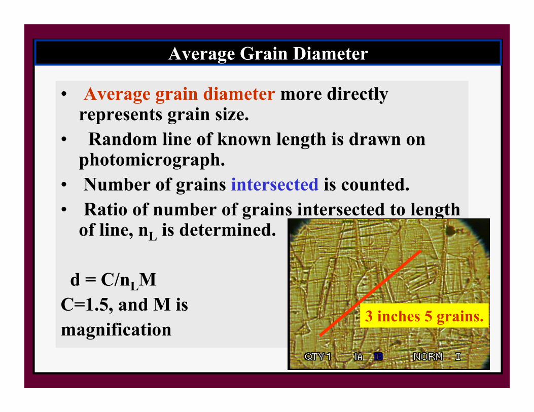
Average Grain Diameter
• Average grain diameter more directly represents grain size.
• Random line of known length is drawn on photomicrograph.
• Number of grains intersected is counted.• Ratio of number of grains intersected to length
of line, nL is determined.
d = C/nLMC=1.5, and M is magnification
3 inches 5 grains.

Effect of Etching
UnetchedSteel200 X
Etched Steel200 X
UnetchedBrass200 X
Etched Brass200 X
4-32
Figure 4.28

Rate Process in Solids
• Reactions occur in solid state resulting in more stableatomic arrangement.
• Reacting atoms must have sufficient energy to overcome activation energy barrier.
• At a given temperature, not all atoms have activation energy E*. It should be supplied to them.
E*
Er
EP
AE*Activation Energy
Energy releasedDue to reaction
Reaction Coordinate
Reactants
Products
Er = Energy of reactantsE* = Activation Energy LevelΔE* = Activation EnergyEp = Energy of Products
4-34
Figure 4.33

Rate Process in Solids (Cont..)
• As temperature increases, more and more atoms acquire activation energy level.
• Probability of finding an atom/molecule with energy E* greater than average energy E of all atoms/ molecules is given by
KTEEe /)*( −−αK = Boltzman’s Constant = 1.38 x 10⁻²³ J/(atom.K).
T = Temperature in Kelvin.
4-35

Rate Process in Solids (Cont..)
• The fraction of atoms having energies greater than E* in a system (when E* is greater than average energy E) is given by
TKE
total
CeN
n.*−
=
n = Number of molecules greater than energy E*Ntotal = Total number of moleculesK = Boltzman’s ConstantC = ConstantT = Temperature in Kelvin.
4-36

Rate Process in Solids (Cont..)
• The number of vacancies at equilibrium at a particular temperature in a metallic crystal lattice is given by
TKE
vV
CeNn
.−
=
nv = Number of vacancies per m3 of metalEv = Activation Energy to form a vacancy T = Absolute Temperature.K = Boltznam,s Constant.C = Constant
4-37
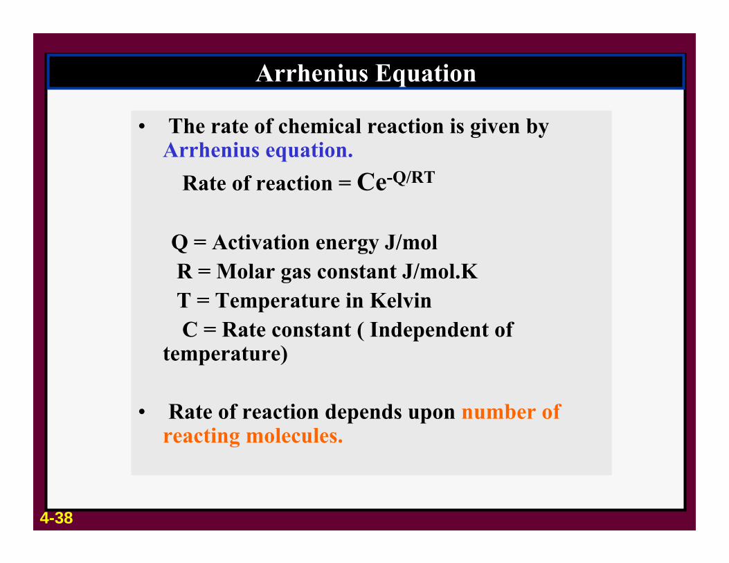
Arrhenius Equation
• The rate of chemical reaction is given by Arrhenius equation.
Rate of reaction = Ce-Q/RT
Q = Activation energy J/molR = Molar gas constant J/mol.KT = Temperature in KelvinC = Rate constant ( Independent of
temperature)
• Rate of reaction depends upon number of reacting molecules.
4-38

Solidification of Metals
• Arrhenius equation can also be written asln (rate) = ln ( C) – Q/RT
Or Log10 (rate) = Log10 (C) – Q/2.303 RT
Which is similar to Y = b + m X
Which is equation of a straight lineWith Y intercept as ‘b’ and slope ‘m’.
Y Log10(rate)X (1/T)b Log10(C)m Q/2.303R
4-39Figure 4.34 Arrhenius plot
(After J. Wulff et al., “Structure and Properties of Materials,” vol. II: “Thermodynamics of Structure,” Wiley, 1964, p.64.)

Diffusion
5-1

Atomic Diffusion in Solids
• Diffusion is a process by which a matter is transported through another matter.
• Examples: Movement of smoke particles in air :
Very fast.Movement of dye in water : Relatively slow.Solid state reactions : Very restricted movement due to bonding.
5-2

Vacancy or Substitutional Diffusion mechanism
• Atoms diffuse in solids ifVacancies or other crystal defects are
presentThere is enough activation energy
• Atoms move into the vacancies present. • More vacancies are created at higher
temperature.• Diffusion rate is higher at high
temperatures.
5-3
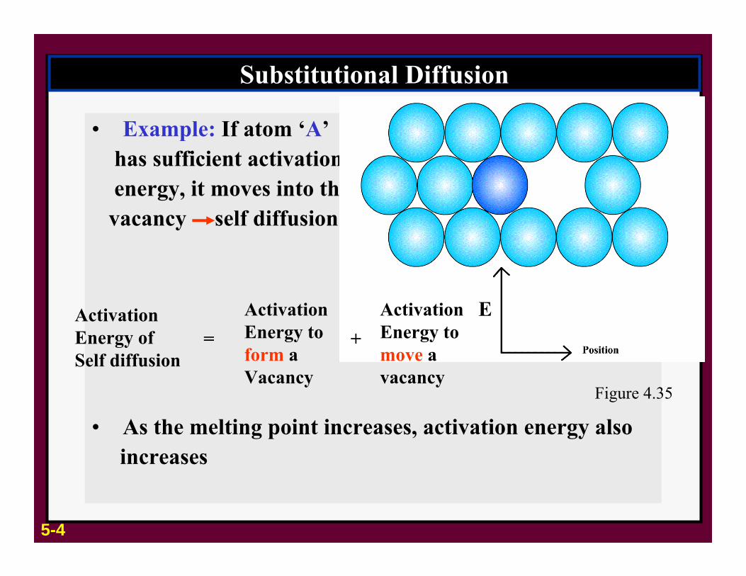
Substitutional Diffusion
• Example: If atom ‘A’has sufficient activationenergy, it moves into thevacancy self diffusion.
• As the melting point increases, activation energy alsoincreases
Activation Energy ofSelf diffusion
ActivationEnergy toform aVacancy
ActivationEnergy tomove a vacancy
= +
Figure 4.35
5-4

Interstitial Diffusion mechanism
• Atoms move from one interstitial site to another.
• The atoms that move mustbe much smaller than thematrix atom.
• Example:Carbon interstitiallydiffuses into BCC α or FCC γ iron. Interstitial atoms
Matrixatoms Figure 4.37
5-5
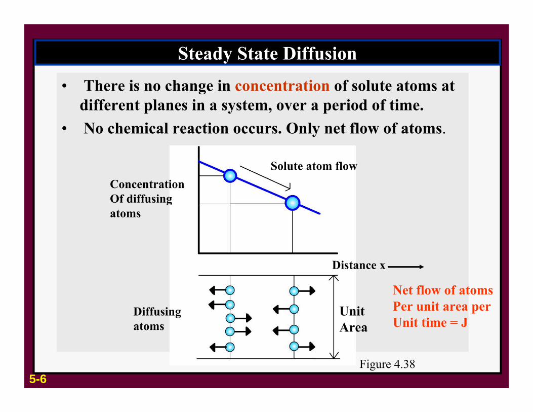
Steady State Diffusion
• There is no change in concentration of solute atoms at different planes in a system, over a period of time.
• No chemical reaction occurs. Only net flow of atoms.
C1
C2
Net flow of atomsPer unit area perUnit time = J
Solute atom flow
Diffusingatoms
UnitArea
ConcentrationOf diffusingatoms
Distance x
Figure 4.385-6
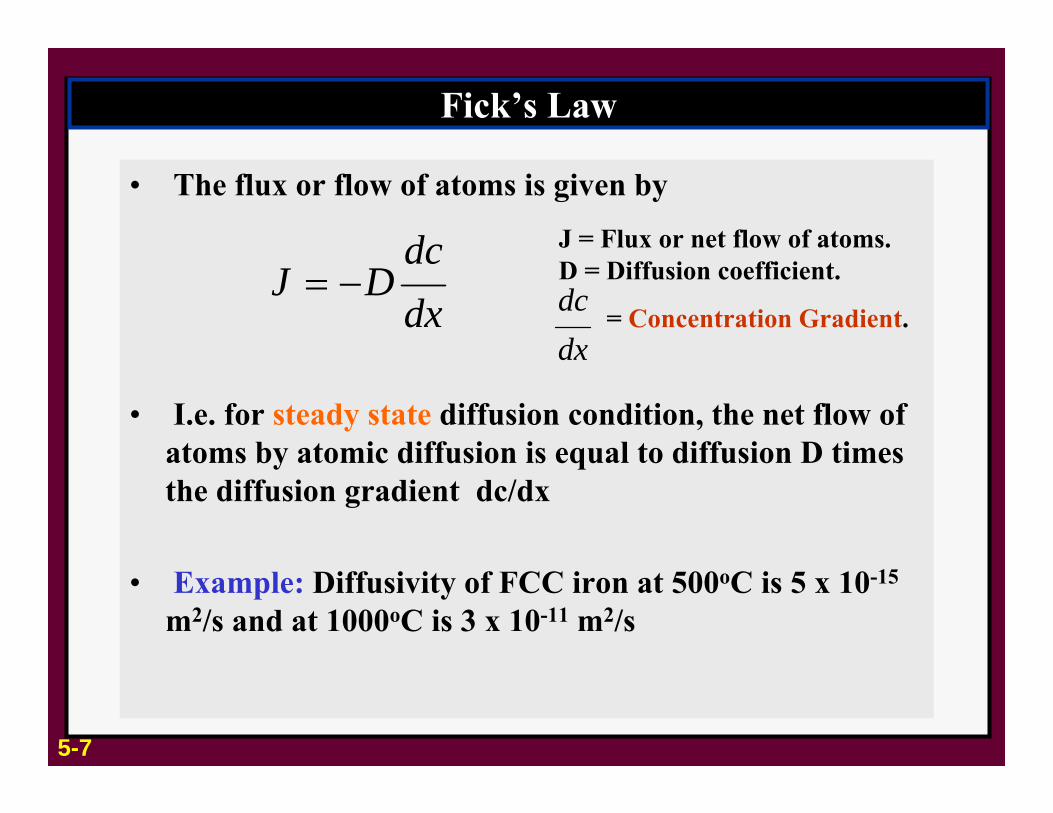
Fick’s Law
• The flux or flow of atoms is given by
• I.e. for steady state diffusion condition, the net flow of atoms by atomic diffusion is equal to diffusion D times the diffusion gradient dc/dx
• Example: Diffusivity of FCC iron at 500oC is 5 x 10-15
m2/s and at 1000oC is 3 x 10-11 m2/s
dxdc
DJ −=J = Flux or net flow of atoms.D = Diffusion coefficient.
dxdc = Concentration Gradient.
5-7

Diffusivity
• Diffusivity depends uponType of diffusion : Whether the diffusion is
interstitial or substitutional.Temperature: As the temperature increases
diffusivity increases.Type of crystal structure: BCC crystal has lower
APF than FCC and hence has higher diffusivity.Type of crystal imperfection: More open
structures (grain boundaries) increases diffusion. The concentration of diffusing species: Higher
concentrations of diffusing solute atoms will affect diffusivity.
5-8

Non-Steady State Diffusion
• Concentration of solute atoms at any point in metal changes with time in this case.
• Ficks second law:- Rate of compositional change is equal to diffusivity times the rate of change of concentration gradient.
⎟⎟⎠
⎞⎜⎜⎝
⎛=
dxdc
Ddxd
dtdC xx
Plane 1 Plane 2
Change of concentration of solute Atoms with change in time in different planes
5-9

Fick’s Second Law – Solution
• Cs = Surface concentration of element in gas diffusinginto the surface.
• C0 = Initial uniform concentrationof element in solid.
• Cx = Concentration of element atdistance x from surface at time t1.
• x = distance from surface• D = diffusivity of solute• t = time.
Distance x
C0
Cx
Cs
Time = t2 - much later
Time= t1 - later
Time = t0
x
⎟⎟⎠
⎞⎜⎜⎝
⎛=
−
−
ts
xs
Dx
erfCCCC
20
Figure 4.39
5-10

Industrial Applications of Diffusion – Case Hardening
• Sliding and rotating parts needs to have hard surfaces.
• These parts are usually machined with low carbon steel as they are easy to machine.
• Their surface is then hardened by carburizing.
• Steel parts are placed at elevated temperature (9270C) in an atmosphere of hydrocarbon gas (CH4).
• Carbon diffuses into iron surface and fills interstitial space to make it harder.
5-11

Carburizing
Low carbonSteel part
Diffusing carbonatoms
C %
Figure 4.43 bCarbon Gradients
In Carburized metals
(After “Metals handbook,” vol.2: “Heat Treating,” 8th ed, American Society of Metals, 1964, p.100)5-12

Impurity Diffusion into Silicon wafer
• Impurities are made to diffuse into silicon wafer to change its electrical characteristics.
• Used in integrated circuits.• Silicon wafer is exposed to vapor of impurity at 11000C
in a quartz tube furnace. • The concentration of
impurity at any point depends on depth and time of exposure.
Figure 4.44
(After W.R. Runyan, “ Silicon Semiconductor Technology,” McGraw-Hill, 1965.)5-13

Effect of Temperature on Diffusion
• Dependence of rate of diffusion on temperature is given by
RTQ
DD
RTQ
DD
eDD RTQ
303.2loglog
lnln
01010
0
0
−=
−=
=−
or
or
D = Diffusivity m2/sD0 = Proportionality constant m2/sQ = Activation energy of diffusing species J/mol R = Molar gas constant = 8.314 J/mol.KT = Temperature (K)
5-14

Effect of Temperature on Diffusion-Example
• If diffusivity at two temperatures are determined, two equations can be solved for Q and D0
• Example:-The diffusivity of silver atoms in silver is 1 x 10-17
at 5000C and 7 x 10-13 at 10000C.Therefore,
molKJQ
RQ
TTRQ
RTQRTQ
DD
/183
7731
12731
exp101107
11exp
)/exp()/exp(
17
13
121
2
500
1000
=
⎟⎟⎠
⎞⎜⎜⎝
⎛⎟⎟⎠
⎞⎜⎜⎝
⎛−−=
×
×
⎟⎟⎠
⎞⎜⎜⎝
⎛⎟⎟⎠
⎞⎜⎜⎝
⎛−
−=
−
−=
−
−
Solving for activation energy Q
5-15

Diffusivity Data for Some Metals
18251 x 10-5HCP Titanium
Carbon
1972 x 10-5CopperCopper
1261.5 x 10-5AluminumCopper
12222 x 10-5BCC IronCarbon
1422 x 10-5FCC IronCarbon
Q KJ/m
ol
D0
(M2/S)SolventSolute
Figure 4.47
(After L.H. Van Vlack. “Elements of Materials Science and Engineering.” 5th ed., Addison-Wesley, 1985. P.137.)5-16

Mechanical PropertiesOf
Metals - I
6-1

Processing of Metals - Casting
• Most metals are first melted in a furnace
• Alloying is done if required
• Large ingots are then cast
• Sheets and plates are then produced from ingots by rolling Wrought alloy products
• Channels and other shapes are produced by extrusion
• Some small parts can be cast as final product
Example :- Automobile Piston
6-2

Casting (Cont..)
Casting Process
Casting mold
Cast parts
Figure 5.3 a Figure 5.3 b
Figure 5.2
6-3

• Hot rolling Greater reduction of thickness in a single pass
• Rolling carried out at above recrystallization temperature
• Ingots preheated to about 12000C. Ingots reheated between passesif required
• Usually, series of 4 high rolling mills are used.
Hot Rolling of Steel
6-4

Cold Rolling of Metal Sheet
• Cold rolling is rolling performed below recrystallization temperature
• This results in strain hardening
• Hot rolled slabs have to be annealed before cold rolling
• Series of 4 high rolling mills are usually used.
• Less reduction of thickness
• Needs high power
Figure 5.86-5

Cold Rolling (Cont..)
% Cold work =Initial metal thickness – Final metal thickness
Initial metal thicknessx 100
Figure 5.6
6-6
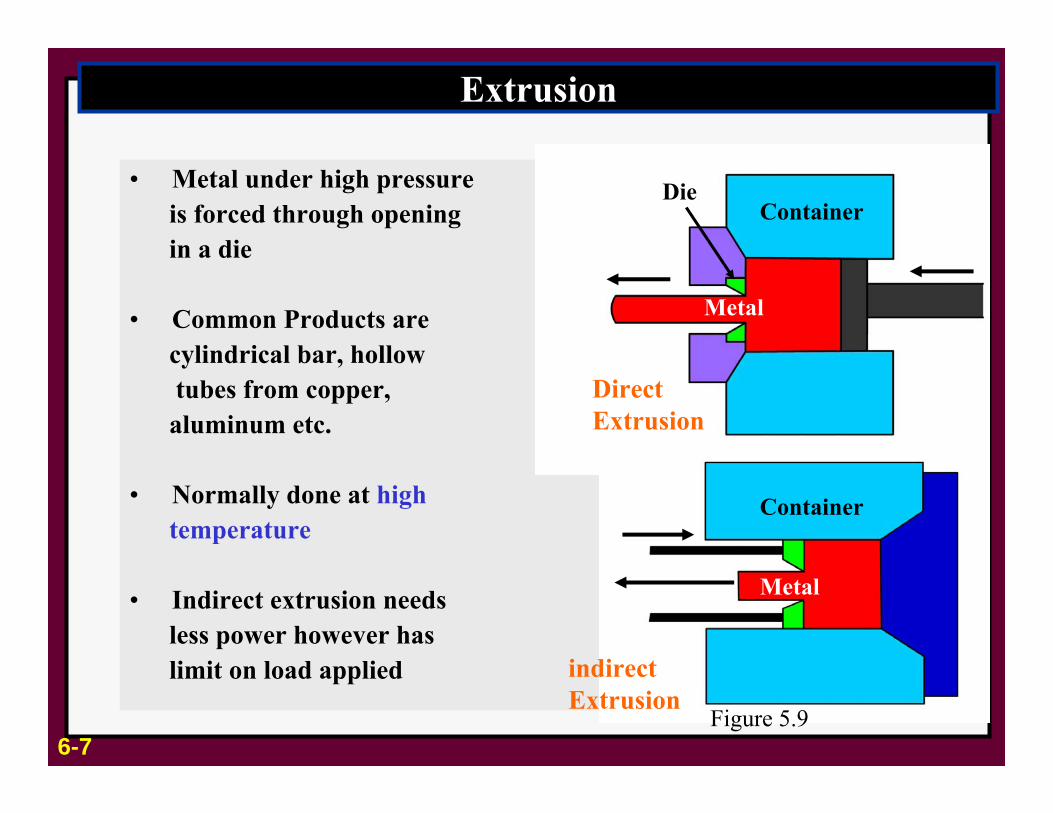
Extrusion
• Metal under high pressure is forced through opening in a die
• Common Products arecylindrical bar, hollowtubes from copper, aluminum etc.
• Normally done at hightemperature
• Indirect extrusion needsless power however haslimit on load applied
Container
Container
Metal
Metal
Die
DirectExtrusion
indirectExtrusion
6-7Figure 5.9
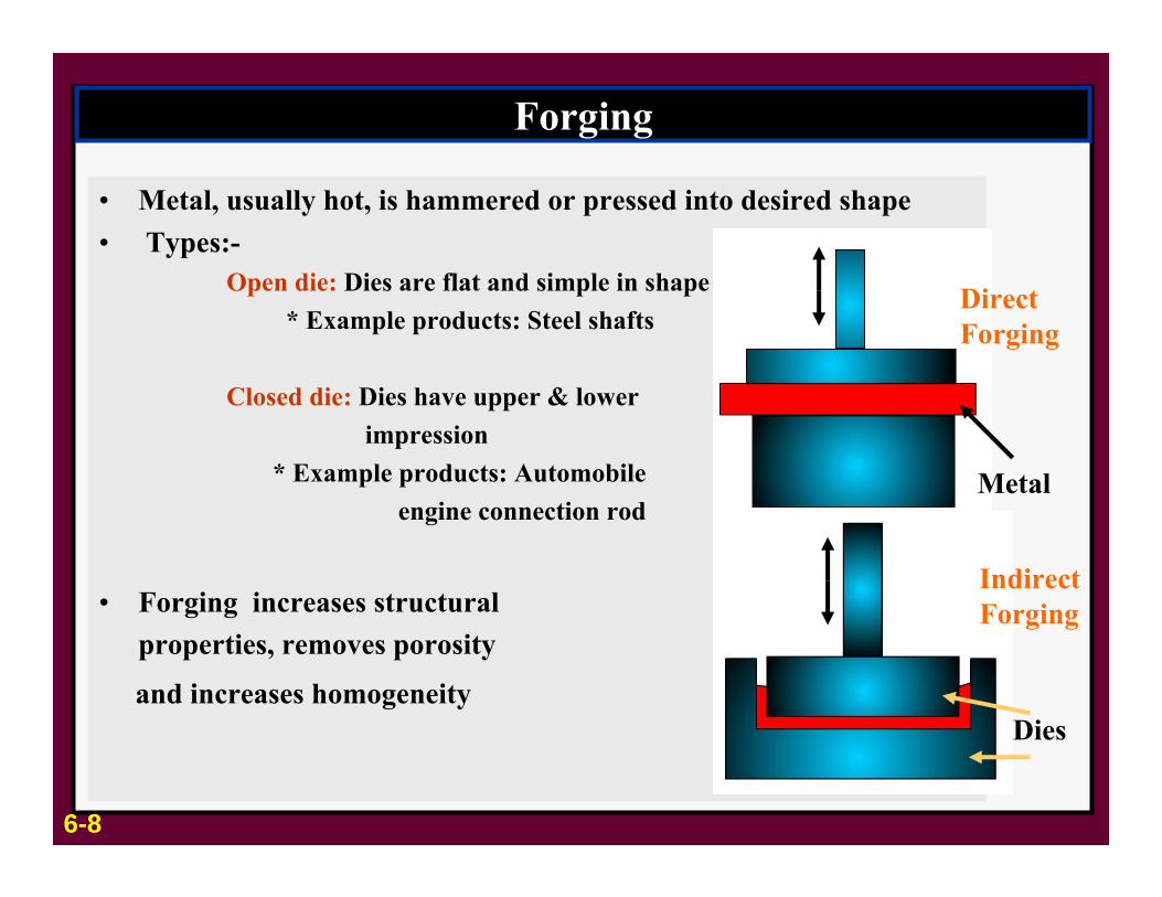
Forging
• Metal, usually hot, is hammered or pressed into desired shape• Types:-
Open die: Dies are flat and simple in shape* Example products: Steel shafts
Closed die: Dies have upper & lowerimpression
* Example products: Automobile engine connection rod
• Forging increases structural properties, removes porosity
and increases homogeneity
Direct Forging
Indirect Forging
Dies
Metal
6-8
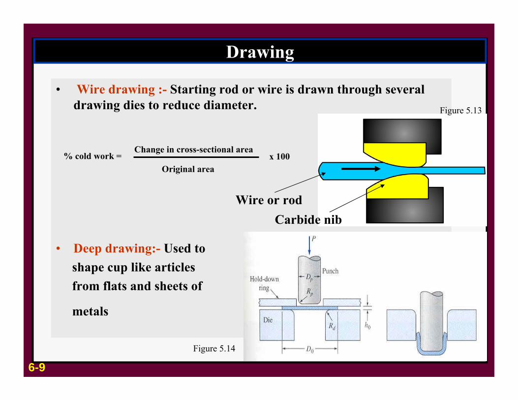
Drawing
• Wire drawing :- Starting rod or wire is drawn through several drawing dies to reduce diameter.
• Deep drawing:- Used to shape cup like articles from flats and sheets of
metals
% cold work =Change in cross-sectional area
Original areax 100
Wire or rodCarbide nib
Figure 5.13
Figure 5.14
6-9

Stress and Strain in Metals
• Metals undergo deformation under uniaxial tensile force.
• Elastic deformation: Metal returns to its original dimension after tensileforce is removed.
• Plastic deformation: Themetal is deformed to such an extent suchthat it cannot returnto its original dimension
Elastic deformation
Plastic deformation
6-10
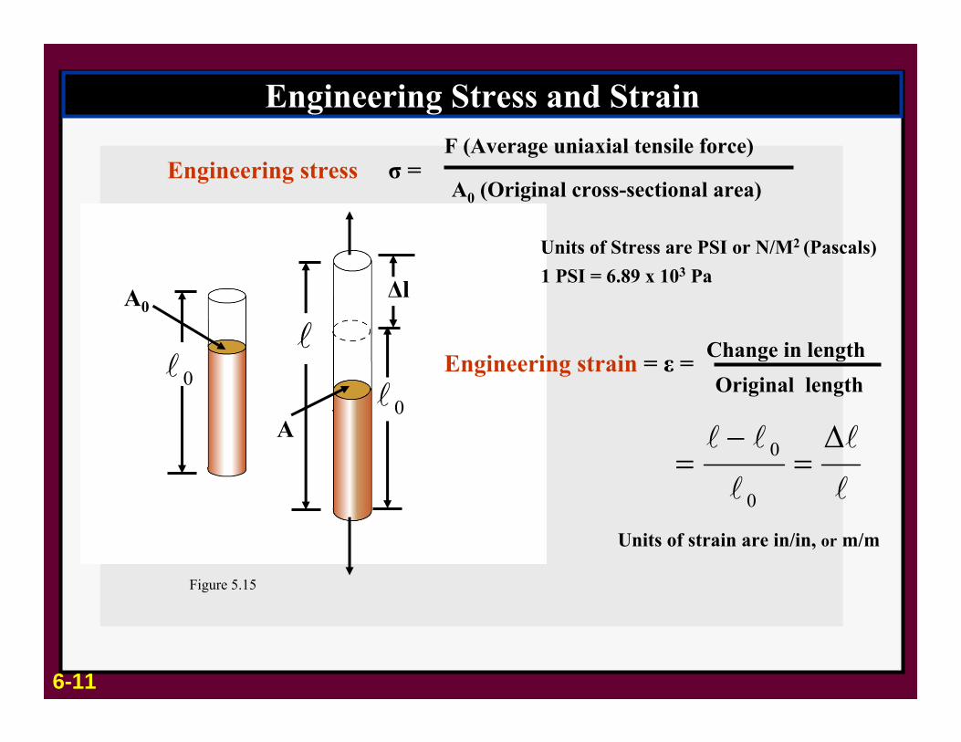
Engineering Stress and Strain
Engineering stress σ =
A0Δl
A
Figure 5.15
F (Average uniaxial tensile force)
A0 (Original cross-sectional area)
Units of Stress are PSI or N/M2 (Pascals)1 PSI = 6.89 x 10³ Pa
Engineering strain = ε = Change in lengthOriginal length
l
l
l
ll Δ=
−=
0
0
l0l
0l
Units of strain are in/in, or m/m
6-11

Poisson’s Ratio
0l lw0 w
.
z
y
allongitudinlateral
εε
εε
ν −=−=)(
)(Poisson’s ratio =
0
0
ll −
−−=
wwν
Usually poisons ratio ranges from0.25 to 0.4.
Example: Stainless steel 0.28Copper 0.33
6-12

Shear Stress and Shear Strain
τ = Shear stress = S (Shear force)A (Area of shear force application)
Shear strain γ = Amount of shear displacementDistance ‘h’ over which shear acts.
Elastic Modulus G = τ / γ
Figure 5.17
6-13

Tensile test
• Strength of materials can be tested by pulling the metal to failure.
SpecimenExtensometer
Force data is obtained from Load cellStrain data is obtained from Extensometer.
Load Cell
Figure 5.18
6-14

Tensile Test (Cont)
Commonly used Test specimen
Typical Stress-straincurve
Figure 5.21
Figure 5.22
6-15

Tensile Test –1045 Steel - Movie
Stress-Strain Curve
6-16

Mechanical Properties
• Modulus of elasticity (E) : Stress and strain are linearly related in elastic region. (Hooks law)
• Higher the bonding strength, higher is the modulus of elasticity.
• Examples: Modulus of Elasticity of steel is 207 Gpa.Modulus of elasticity of Aluminum is 76 Gpa
E = σ (Stress)
ε (Strain)
Stress
Strain
Linear portion of thestress strain curve
Δε
ΔσE =
ΔσΔε
6-17

Yield Strength
• Yield strength is strength at which metal or alloy shows significant amount of plastic deformation
• 0.2% offset yield strength is thatstrength at which 0.2% plasticdeformation takes place
• A line, starting at 0.2%strain and parallel to elastic regionis drawn to obtain the 0.2% offset yield strength
Figure 5.23
6-18

Ultimate tensile strength
• Ultimate tensile strength (UTS) is the maximum strength reachedby the engineering stress strain curve.
• Necking starts after UTS is reached
• More ductile the metal is, moreis the necking before failure
• Stress increases till failure. Dropin stress strain curve is due to stress
calculation based on original area.
Al 2024-Annealed
Al 2024-TemperedSt re s s
Mpa
Strain
Necking Point
Stress strain curves of Al 2024 With two different heattreatments. Ductile annealed sample necks more
Figure 5.24
6-19

Percent Elongation
• Percent elongation is a measure of ductility of a material.
• It is the elongation of the metal before fracture expressed as percentage of original length.
% Elongation =
• Measured using a caliper fitting the fractured metal together.
• Example:- Percent elongation of pure aluminum is 35%For 7076-T6 aluminum alloy it is 11%
Final length – initial Length
Initial Length
6-20
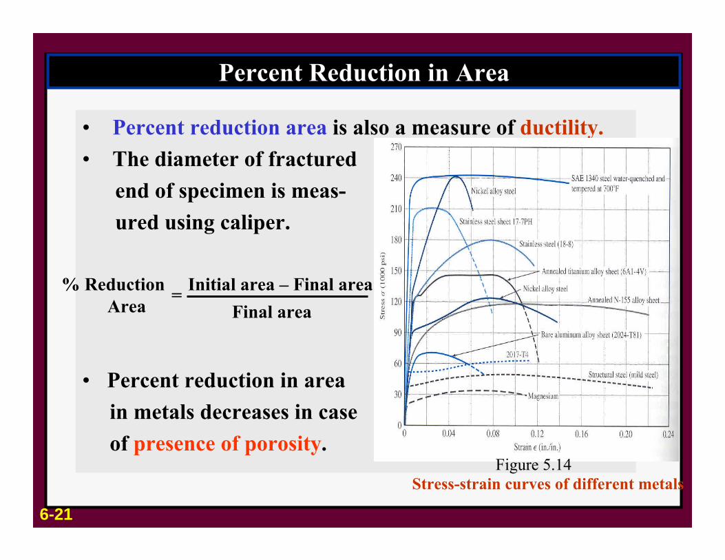
Percent Reduction in Area
• Percent reduction area is also a measure of ductility.• The diameter of fractured
end of specimen is meas-ured using caliper.
• Percent reduction in areain metals decreases in caseof presence of porosity.
% ReductionArea = Initial area – Final area
Final area
Figure 5.14Stress-strain curves of different metals
6-21
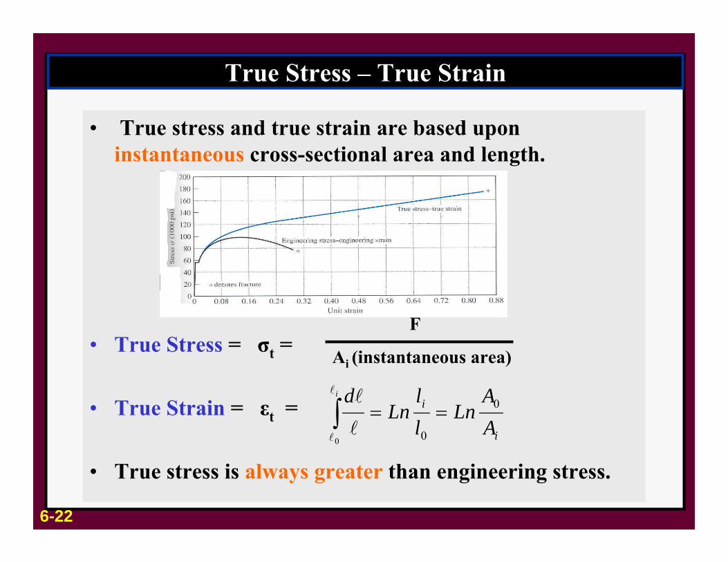
True Stress – True Strain
• True stress and true strain are based upon instantaneous cross-sectional area and length.
• True Stress = σt =
• True Strain = εt =
• True stress is always greater than engineering stress.
F
Ai (instantaneous area)
i
i
AA
Lnll
Lndi
0
00
==∫l
ll
l
6-22

Tensile Test – 1018 Steel (Low Carbon)
Tensile strength = 440 Mpa Modulus of Elasticity = 205 GpaReduction in area = 40%, Elongation = 15%
6-23

Tensile Test 1090 Steel (High Carbon)
Tensile Strength = 696 Mpa, Elastic Modulus = 207 GpaArea reduction = 40%, Elongation = 10%
6-24

Tensile Test – 6064-O Aluminum (Annealed)
Ultimate tensile strength = 89 MPa, Modulus of elasticity = 69 GpaReduction in area = 68%, Elongation = 28%
6-25

Tensile Test – 6064-T6 Aluminum (Tempered)
Ultimate tensile strength = 241 MPa, Elastic Modulus = 69 GpaArea reduction = 48%, Elongation = 15%
6-26

Hardness and Hardness Testing
• Hardness is a measure of the resistance of a metal to permanent (plastic) deformation.
• General procedure:
Press the indenter thatis harder than the metal
Into metal surface.
Withdraw the indenter
Measure hardness by measuring depth or
width of indentation.Figure 5.27
Rockwell hardnesstester
6-27

Hardness Tests
Table 5.26-28

Plastic Deformation in Single Crystals
• Plastic deformation of single crystal results in step markings on surface slip bands.
• Atoms on specific crystallographic planes (slip planes)slip to cause slip bands.
Figure 5.28
Slip bands
6-29

Slip Bands and Slip Planes
• Slip bands in ductile metals are uniform (occurs in many slip planes).
• Slip occurs in many slip planes within slip bands.
• Slip planes areabout 200A thickand are offset byabout 2000A
Figure 5.306-30

Slip Mechanism
• During shear, atoms do not slide over each other.• The slip occurs due to movement of dislocations.
Dislocation cell structure in lightlydeformed Aluminum
Figure 5.33
Figure 5.32
Wall of high dislocation density
6-31
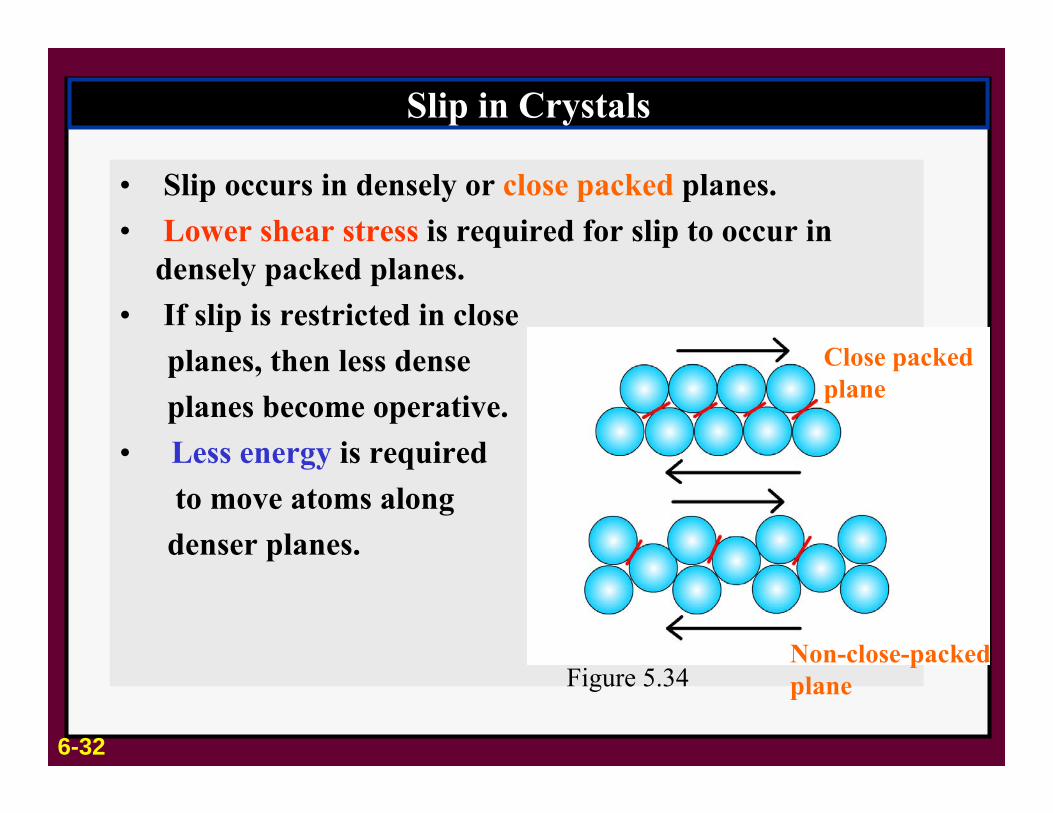
Slip in Crystals
• Slip occurs in densely or close packed planes.• Lower shear stress is required for slip to occur in
densely packed planes.• If slip is restricted in close
planes, then less dense planes become operative.
• Less energy is requiredto move atoms alongdenser planes.
Close packedplane
Non-close-packedplaneFigure 5.34
6-32

Slip Systems
• Slip systems are combination of slip planes and slip direction.
• Each crystal has a number of characteristic slip systems.
• In FCC crystal, slip takes place in 111 octahedral planes and <110> directions.
4 (111) type planes and 3 [110] type directions.4 x 3 = 12 slip systems.
Table 5.36-33

Slip Systems in BCC Crystal
• BCC crystals are not close packed. The slip predominantly occurs in 110 planes that has highest atomic density.
Table 5.3
6-34

Slip Systems in HCP Crystal
• If HCP crystals have high c/a ratio, slip occurs along basal planes 0001. For crystals with low c/a ratio, slip also occurs in 1010 and 1011 planes.
Table 5.3
6-35

Critical Resolved Shear Stress
• Critical resolved shear stress is the stress required to cause slip in pure metal single crystal.
• Depends upon Crystal StructureAtomic bonding characteristicsTemperature Orientation of slip planes relative to shear stress
• Slip begins when shear stress in slip plane in slip direction reaches critical resolved shear stress.
• This is equivalent to yield stress.• Example :- Zn HCP 99.999% pure 0.18MPa
Ti HCP 99.99% pure 13.7 MPaTi HCP 99.9% pure 90.1 MPa
6-36

Schmid’s Law
• The relationship between uniaxial stress action on a single cylinder of pure metal single crystal and resulting resolved shear stress produced on a slip system is give by
τr= τr=Shear ForceShear Area
Φ=== CosCosAF
CosACosF
AFr .
/.
001
λλ
λ
Φ= CosCos .. λσ
1AFr
r =τ
Slipdirection
Normal toSlip plane Φ
λ
0AF
=σ
A1=Area ofSlip plane
6-37

Twinning
• In twinning, a part of atomic lattice is deformed and forms mirror image of lattice next to it
• Distance moved by atoms is proportional to their distance from twinning plane
• Deformation from twinning is small.
• Twinning reorientthe slip system
6-38

Effects of Grain Boundaries on Strength
• Grain boundaries stop dislocation movement and hence strengthen the metals.
• Fine grain size is desirable, and hence metals are produced with finer grains.
Figure 5.40 Figure 5.40 Figure 5.40Stress-strain curve of singleand polycrystalline copper
Slip bands in polycrystallinealuminum grains
Dislocations piled up against grain boundaries in stainless steel
6-39
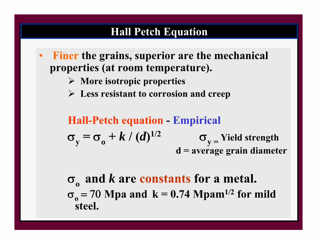
Hall Petch Equation
• Finer the grains, superior are the mechanical properties (at room temperature).
More isotropic propertiesLess resistant to corrosion and creep
Hall-Petch equation - Empiricalσy = σo + k / (d)1/2 σy = Yield strength
d = average grain diameter
σo and k are constants for a metal.σo = 70 Mpa and k = 0.74 Mpam1/2 for mild
steel.

Effects of Plastic Deformation
• Plastic deformation results in shearing of grains relative to each other.
• The grains elongate in rolling direction.• Dislocations get rearranged.
Grain structure atdifferent regions ofcartridge brassrolled into a wedge
6-40

Effect of Cold Work on Tensile Strength
• Number of dislocations are increased by cold work. • Dislocation movements are hindered by both grain
boundaries and other dislocations Strain Hardening
Stress-Strain curves of 1018 steel
1018-Cold Rolled
1018-Annealed
Figure 5.456-41

Solid Solution Strengthening
• Addition of one or more metals can increase the strength of metals.
• Solute atoms, on case of substitutional solid solution, create stress fields around themselves and hinder the dislocation movement.
• Distortion of lattice and clustering of like atoms also impede dislocation movement.
• Example: Solid solution of 70 wt % Cu & 30 wt % Zn (cartridge brass) has tensile strength of 500 MPa. Tensile strength of unalloyed copper is 330 MPa
6-42

Superplasticity in Metals
• At elevated temperature and slow loading, some alloys deform 2000%.
• Annealed Ti alloyElongates 12% at room temperatureElongates up to 1170% at 870oC and 1.3x10⁻⁴/sloading rate.
• Conditions: very fine grain size (5-10 microns)* Highly strain sensitive* Temperature above 0.5 Tm* Slow strain rate

Mechanism of Superplasticity
• Very limited dislocation activity• Deformation mechanism:
Grain boundary slidingGrain boundary diffusionSliding and rotation of individual grains.
• Applications: Metalforming operations.
Blow forming to produce automobilehoods.
Grains before and after deformation
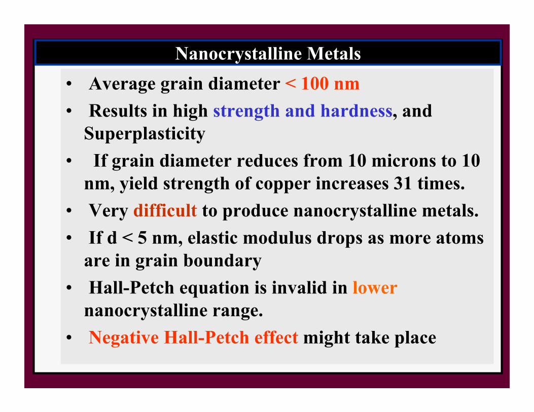
Nanocrystalline Metals• Average grain diameter < 100 nm• Results in high strength and hardness, and
Superplasticity• If grain diameter reduces from 10 microns to 10
nm, yield strength of copper increases 31 times.• Very difficult to produce nanocrystalline metals.• If d < 5 nm, elastic modulus drops as more atoms
are in grain boundary• Hall-Petch equation is invalid in lower
nanocrystalline range.• Negative Hall-Petch effect might take place


![Solidification · 2017-09-12 · solidification. 0.2 kBTm for homogenous nucleation in pure metals [4]. The addition of foreign substrates in the melt provides nucleation sites with](https://static.fdocuments.in/doc/165x107/5ec892b94b6bd71ac95ffd98/solidification-2017-09-12-solidification-02-kbtm-for-homogenous-nucleation-in.jpg)