Lecture 3 OUTLINE Semiconductor Fundamentals (cont’d) – Thermal equilibrium – Fermi-Dirac...
24
Lecture 3 OUTLINE • Semiconductor Fundamentals (cont’d) – Thermal equilibrium – Fermi-Dirac distribution • Boltzmann approximation – Relationship between E F and n, p – Degenerately doped semiconductor Reading : Pierret 2.4-2.5; Hu 1.7-1.10
-
Upload
darren-greene -
Category
Documents
-
view
218 -
download
1
Transcript of Lecture 3 OUTLINE Semiconductor Fundamentals (cont’d) – Thermal equilibrium – Fermi-Dirac...
Lecture 3
OUTLINE• Semiconductor Fundamentals (cont’d)– Thermal equilibrium– Fermi-Dirac distribution• Boltzmann approximation
– Relationship between EF and n, p
– Degenerately doped semiconductor
Reading: Pierret 2.4-2.5; Hu 1.7-1.10

Thermal Equilibrium• No external forces are applied:– electric field = 0, magnetic field = 0– mechanical stress = 0– no light
• Dynamic situation in which every process is balanced by its inverse processElectron-hole pair (EHP) generation rate = EHP recombination rate
• Thermal agitation electrons and holes exchange energy with the crystal lattice and each other Every energy state in the conduction band and valence band
has a certain probability of being occupied by an electron
EE130/230M Spring 2013 Lecture 3, Slide 2

Analogy for Thermal Equilibrium
• There is a certain probability for the electrons in the conduction band to occupy high-energy states under the agitation of thermal energy (vibrating atoms).
Sand particles
EE130/230M Spring 2013 Lecture 3, Slide 3

Fermi Function
kTEE FeEf /)(1
1)(
EE130/230M Spring 2013 Lecture 3, Slide 4
• Probability that an available state at energy E is occupied:
• EF is called the Fermi energy or the Fermi level
There is only one Fermi level in a system at equilibrium.
If E >> EF :
If E << EF :
If E = EF :
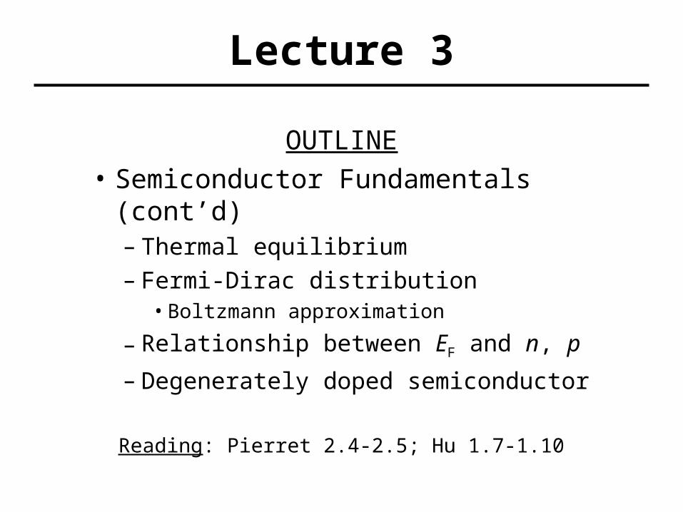
Effect of Temperature on f(E)
EE130/230M Spring 2013 Lecture 3, Slide 5

Boltzmann Approximation
EE130/230M Spring 2013 Lecture 3, Slide 6
Probability that a state is empty (i.e. occupied by a hole):
kTEEF
FeEfkTEE /)()( ,3 If
kTEEF
FeEfkTEE /)(1)( ,3 If
kTEEkTEE FF eeEf /)(/)()(1

Equilibrium Distribution of Carriers• Obtain n(E) by multiplying gc(E) and f(E)
Energy banddiagram
EE130/230M Spring 2013 Lecture 3, Slide 7
Density ofStates, gc(E)
Probability ofoccupancy, f(E)
Carrier distribution, n(E)× =
cnx.org/content/m13458/latest

• Obtain p(E) by multiplying gv(E) and 1-f(E)
Energy banddiagram
EE130/230M Spring 2013 Lecture 3, Slide 8
Density ofStates, gv(E)
Probability ofoccupancy, 1-f(E)
Carrier distribution, p(E)× =
cnx.org/content/m13458/latest

Equilibrium Carrier Concentrations
EE130/230M Spring 2013 Lecture 3, Slide 9
• By using the Boltzmann approximation, and extending the integration limit to , we obtain
band conduction of top
cE
c(E)f(E)dEgn
2/3
2
*, /)( 2
2 where
h
kTmNeNn DOSnc
kTEEc
Fc
• Integrate n(E) over all the energies in the conduction band to obtain n:
EE130/230M Spring 2013 Lecture 3, Slide 10
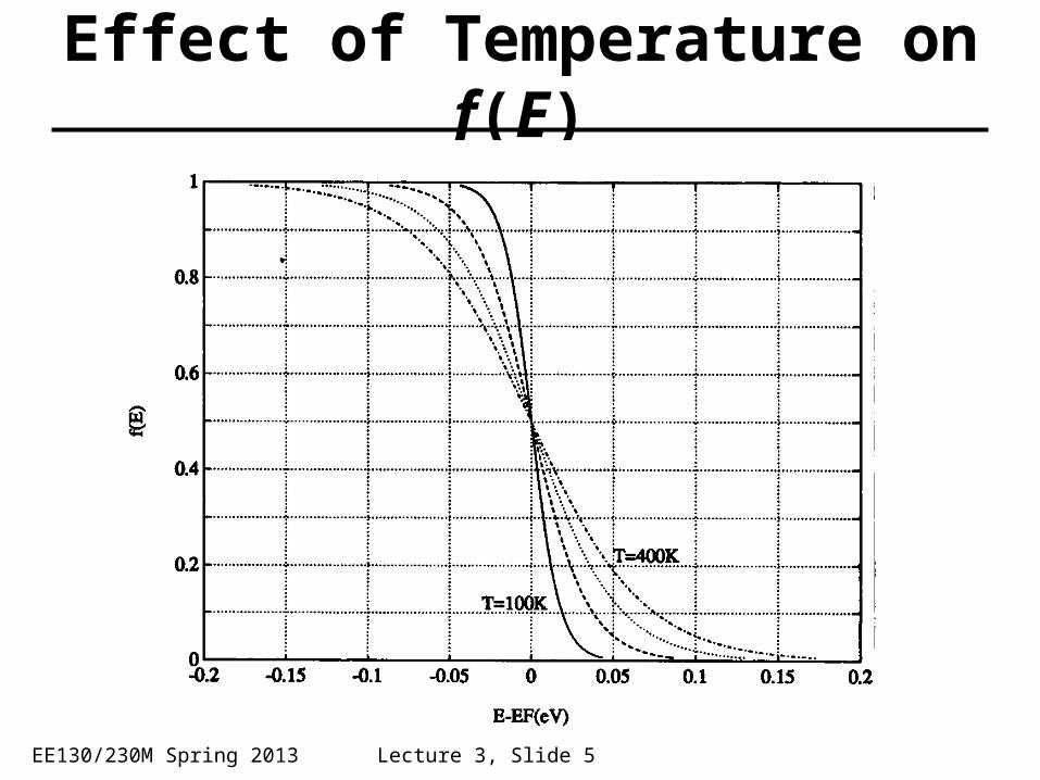
• By using the Boltzmann approximation, and extending the integration limit to -, we obtain
1band valenceof bottom vE
v dEf(E)(E)gp
2/3
2
*, /)( 2
2 where
h
kTmNeNp DOSpv
kTEEv
vF
• Integrate p(E) over all the energies in the valence band to obtain p:

Intrinsic Carrier Concentration
2 / /)(
/)( /)(
ikTE
vckTEE
vc
kTEEv
kTEEc
neNNeNN
eNeNnpGvc
vFFc
2/ kTEvci
GeNNn
EE130/230M Spring 2013 Lecture 3, Slide 11
Si Ge GaAsNc (cm-3) 2.8 × 10¹⁹ 1.04 × 10¹⁹ 4.7 × 10¹⁷
Nv (cm-3) 1.04 × 10¹⁹ 6.0 × 10¹⁸ 7.0 × 10¹⁸
Effective Densities of States at the Band Edges (@ 300K)

n(ni, Ei) and p(ni, Ei)
• In an intrinsic semiconductor, n = p = ni and EF = Ei
/)(
/)(
kTEEic
kTEEci
ic
ic
enN
eNnn
/)(
/)(
kTEEiv
kTEEvi
vi
vi
enN
eNnp
/)( kTEEi
iFenn /)( kTEEi
Fienp
EE130/230M Spring 2013 Lecture 3, Slide 12

Intrinsic Fermi Level, Ei
• To find EF for an intrinsic semiconductor, use the fact that n = p:
2ln
4
3
2
ln22
*,
*,
/)( /)(
vc
DOSn
DOSpvci
ic
vvcF
kTEEv
kTEEc
EE
m
mkTEEE
EN
NkTEEE
eNeN vFFc
EE130/230M Spring 2013 Lecture 3, Slide 13

n-type Material
Energy banddiagram
Density ofStates
Probabilityof occupancy
Carrier distributions
EE130/230M Spring 2013 Lecture 3, Slide 14

Example: Energy-band diagramQuestion: Where is EF for n = 1017 cm-3 (at 300 K) ?
EE130/230M Spring 2013 Lecture 3, Slide 15

Example: Dopant Ionization
EE130/230M Spring 2013 Lecture 3, Slide 16
Probability of non-ionization
meVEn
NkTEE c
ccF 150ln
kTEE FDe /)(1
1
Consider a phosphorus-doped Si sample at 300K with ND = 1017 cm-3.
What fraction of the donors are not ionized?
Hint: Suppose at first that all of the donor atoms are ionized.
017.01
126/)45150(
meVmeVmeVe
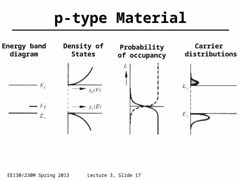
p-type Material
Energy banddiagram
Density ofStates
Probabilityof occupancy
Carrier distributions
EE130/230M Spring 2013 Lecture 3, Slide 17

Non-degenerately Doped Semiconductor
EE130/230M Spring 2013 Lecture 3, Slide 18
• Recall that the expressions for n and p were derived using the Boltzmann approximation, i.e. we assumed
kTEEkTE cFv 33
Ec
Ev
3kT
3kT
EF in this range
The semiconductor is said to be non-degenerately doped in this case.

Degenerately Doped Semiconductor• If a semiconductor is very heavily doped, the Boltzmann
approximation is not valid.
In Si at T=300K: Ec-EF < 3kBT if ND > 1.6x1018 cm-3
EF-Ev < 3kBT if NA > 9.1x1017 cm-3
The semiconductor is said to be degenerately doped in this case.
• Terminology:
“n+” degenerately n-type doped. EF Ec
“p+” degenerately p-type doped. EF Ev
EE130/230M Spring 2013 Lecture 3, Slide 19
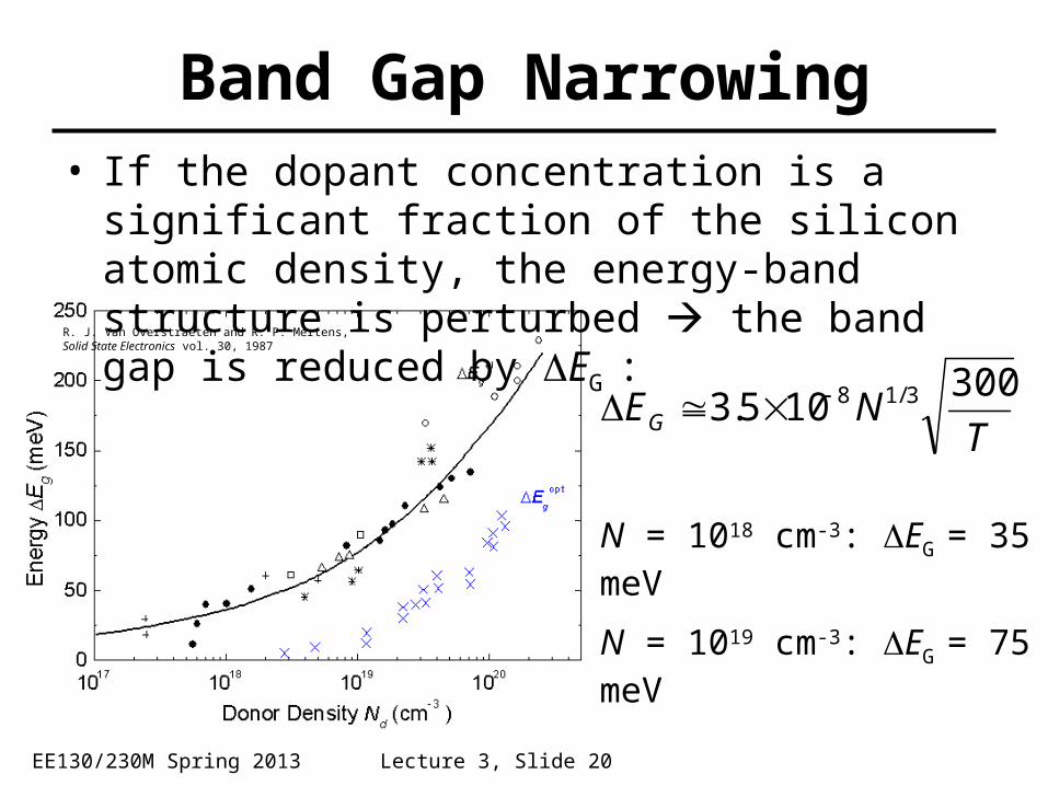
Band Gap Narrowing• If the dopant concentration is a significant fraction of
the silicon atomic density, the energy-band structure is perturbed the band gap is reduced by EG :
N = 1018 cm-3: EG = 35 meV
N = 1019 cm-3: EG = 75 meV
TNEG
300105.3 3/18
EE130/230M Spring 2013 Lecture 3, Slide 20
R. J. Van Overstraeten and R. P. Mertens, Solid State Electronics vol. 30, 1987
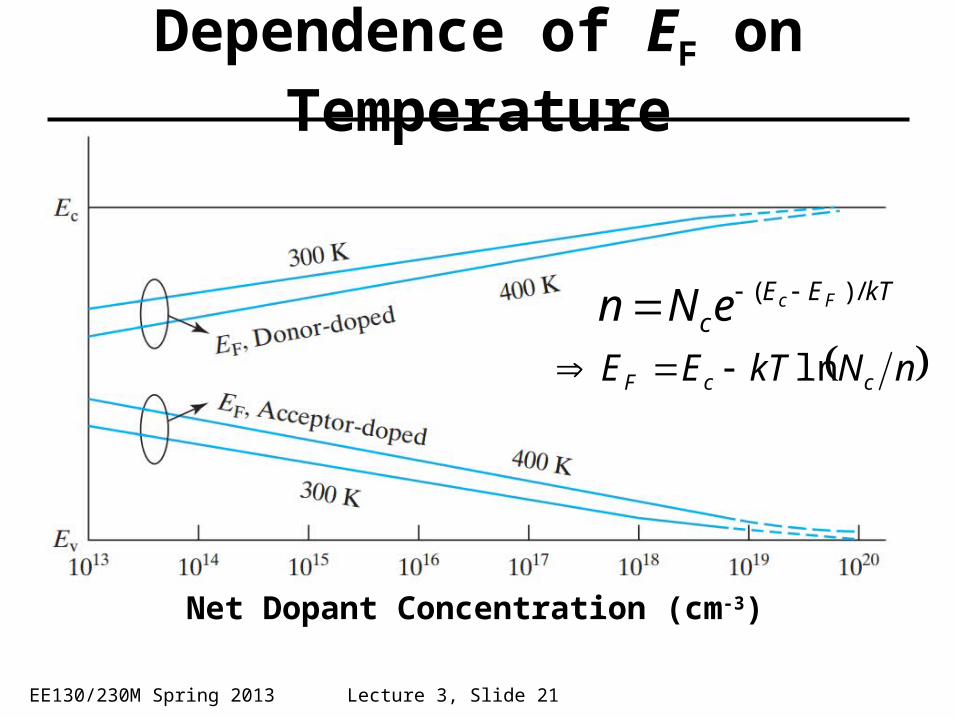
Dependence of EF on Temperature
kTEEc
FceNn /)( nNkTEE ccF ln
Net Dopant Concentration (cm-3)
EE130/230M Spring 2013 Lecture 3, Slide 21

Summary• Thermal equilibrium:– Balance between internal processes with no external
stimulus (no electric field, no light, etc.)
– Fermi function
• Probability that a state at energy E is filled with an electron, under equilibrium conditions.• Boltzmann approximation:
For high E, i.e. E – EF > 3kT:
For low E, i.e. EF – E > 3kT:
kTEE FeEf /)(1
1)(
kTEE FeEf /)()(
kTEEFeEf /)()(1 EE130/230M Spring 2013 Lecture 3, Slide 22

Summary (cont’d)• Relationship between EF and n, p :
• Intrinsic carrier concentration :
• The intrinsic Fermi level, Ei, is located near midgap.
/)( /)( kTEEi
kTEEv
FivF eneNp
/)( /)( kTEEi
kTEEc
iFFc eneNn
2/ kTEvci
GeNNn
EE130/230M Spring 2013 Lecture 3, Slide 23

Summary (cont’d)
EE130/230M Spring 2013 Lecture 3, Slide 24
• If the dopant concentration exceeds 1018 cm-3, silicon is said to be degenerately doped.– The simple formulas relating n and p exponentially to EF
are not valid in this case.
For degenerately doped n-type (n+) Si: EF Ec
For degenerately doped p-type (p+) Si: EF Ev