Lecture 3: Cache & I/OTDTS10/lectures/16/lec3.pdfLecture 3: Cache & I/O ... segments of program and...
22
2016-11-07 1 1 Zebo Peng, IDA, LiTH Zebo Peng, IDA, LiTH TDTS10 – Lecture 3 TDTS10 – Lecture 3 Lecture 3: Cache & I/O Virtual memory Cache memory I/O operations 2 Zebo Peng, IDA, LiTH Zebo Peng, IDA, LiTH TDTS10 – Lecture 3 TDTS10 – Lecture 3 Mismatch of CPU and MM Speeds 1955 1985 1965 1970 1975 1980 1990 2000 2005 1960 Cycle Time (nano second) 10 4 10 3 10 2 10 1 0 Speed Gap (ca. one order of magnitude, i.e., 10 times) 2010 2015
Transcript of Lecture 3: Cache & I/OTDTS10/lectures/16/lec3.pdfLecture 3: Cache & I/O ... segments of program and...

2016-11-07
1
11Zebo Peng, IDA, LiTHZebo Peng, IDA, LiTH TDTS10 – Lecture 3TDTS10 – Lecture 3
Lecture 3: Cache & I/O
Virtual memory
Cache memory
I/O operations
22Zebo Peng, IDA, LiTHZebo Peng, IDA, LiTH TDTS10 – Lecture 3TDTS10 – Lecture 3
Mismatch of CPU and MM Speeds
1955 19851965 1970 1975 1980 1990 2000 20051960
Cyc
le T
ime
(nan
ose
cond
)
104
103
102
101
0
Speed Gap(ca. one orderof magnitude, i.e., 10 times)
2010 2015

2016-11-07
2
33Zebo Peng, IDA, LiTHZebo Peng, IDA, LiTH TDTS10 – Lecture 3TDTS10 – Lecture 3
instructionsand dataaddresses
addresses
instructionsand data
instructionsand data
addresses
Cache Memory
A cache is a very fast memory which is put between the main memory and the CPU, and used to hold segments of program and data of the main memory.
Main MemoryCPU
Cache
44Zebo Peng, IDA, LiTHZebo Peng, IDA, LiTH TDTS10 – Lecture 3TDTS10 – Lecture 3
Zebo’s Cache Memory Model
Personal library for a high-speed reader
A computer is a “predictable and iterative reader.” High cache hit ratio, e.g., 96%, is achievable, even with a
relatively small cache (e.g., 0.1% of memory size).
Storage cells Memory controllerCache

2016-11-07
3
55Zebo Peng, IDA, LiTHZebo Peng, IDA, LiTH TDTS10 – Lecture 3TDTS10 – Lecture 3
Cache Memory Features
It is transparent to the programmers. The CPU still refers to the instructions/data by their addresses in the MM.
Only a very small part of the program/data in the main memory has its copy in the cache (e.g., 4MB cache with 8GB memory).
If the CPU wants to access program/data not in the cache (called a cache miss), the relevant block of the main memory will be copied into the cache.
The intermediate-future memory access will usually refer to the same word or words in the neighborhood, and will not have to involve the main memory.
Locality of reference!
66Zebo Peng, IDA, LiTHZebo Peng, IDA, LiTH TDTS10 – Lecture 3TDTS10 – Lecture 3
Cache Memory Performance
Average Access Time (AAT)
Phit x Tcache_access +
(1 – Phit) x (Tmm_access + Tcache_access) x Block_size +
Tchecking
Ex. A computer has 8MB MM with 100 ns access time, 8KB cache with 10 ns access time, BS=4, and Tchecking = 2.1 ns, Phit = 0.97, AAT will be 25 ns.
Phit = the probability of cache hit, cache hit ratio;Tcache_access = cache access time;Tmm_access = main memory access time;Block_size = number of words in a cache block; andTchecking = the time needed to check for cache hit or miss.
where
2016-11-07
4
77Zebo Peng, IDA, LiTHZebo Peng, IDA, LiTH TDTS10 – Lecture 3TDTS10 – Lecture 3
Cache Memory Performance
Ex. A computer has 8MB MM with 100 ns access time, 8KB cache with 10 ns access time, BS=4, and Tchecking = 2.1 ns, Phit = 0.97, AAT will be 25 ns.
Main Memory[8 MB, 100 ns]
Cache [8 KB, 10 ns]
Composite
Memory[8 MB, 25 ns]
88Zebo Peng, IDA, LiTHZebo Peng, IDA, LiTH TDTS10 – Lecture 3TDTS10 – Lecture 3
Cache Design
The size and nature of the copied block must be care-fully designed, as well as the algorithm to decide which block to be removed from the cache when it is full:
Cache block size (line size).
Total cache size.
Mapping function.
Replacement method.
Write policy.
Numbers of caches:
• Single, two-level, or three-level cache.
• Unified vs. split cache.
2016-11-07
5
99Zebo Peng, IDA, LiTHZebo Peng, IDA, LiTH TDTS10 – Lecture 3TDTS10 – Lecture 3
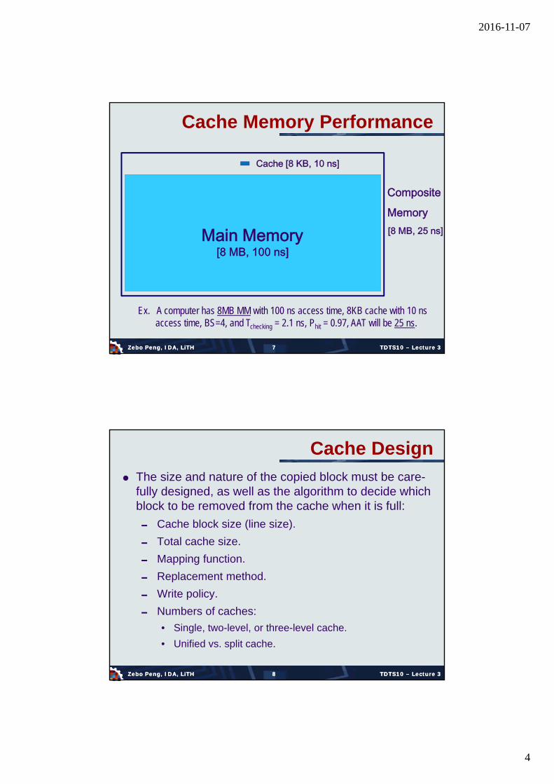
Split Data and Instruction Caches?
Split caches (Harvard Architectures):+ CPU accesses I-cache for instruction fetch, and D-cache for
data.
+ Competition for the cache between instruction processing and execution units is eliminated.
+ Instruction fetch can proceed in parallel with memory access from the CPU for operands.
One may be overloaded while the other is under utilized.
Unified caches:+ Better balance the load between instruction and data fetches
depending on the dynamics of the program execution.
+ Design and implementation are cheaper.
Lower performance.
1010Zebo Peng, IDA, LiTHZebo Peng, IDA, LiTH TDTS10 – Lecture 3TDTS10 – Lecture 3
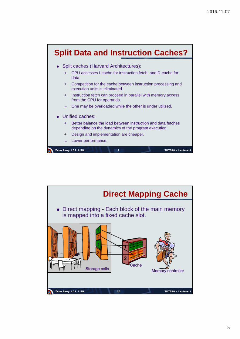
Direct Mapping Cache
Direct mapping - Each block of the main memory is mapped into a fixed cache slot.
Storage cells Memory controllerCache
1
2
12
1
2
2016-11-07
6
1111Zebo Peng, IDA, LiTHZebo Peng, IDA, LiTH TDTS10 – Lecture 3TDTS10 – Lecture 3
Direct Mapping Cache ExampleWe have a 10,000-word MM and a 100-word cache. 10 memory cells are grouped into a block.
Memory address = 2 1 1Tag Slot Word
100-Word Cache
Tag Slot No.9876543210
90-9980-8970-7966-6950-5940-4930-3920-2910-1900-09
0020-00290010-00190000-0009
9990-9999
0120-01290110-01190100-0109
10,000-Word Memory
0 1 1 5
01
1212Zebo Peng, IDA, LiTHZebo Peng, IDA, LiTH TDTS10 – Lecture 3TDTS10 – Lecture 3
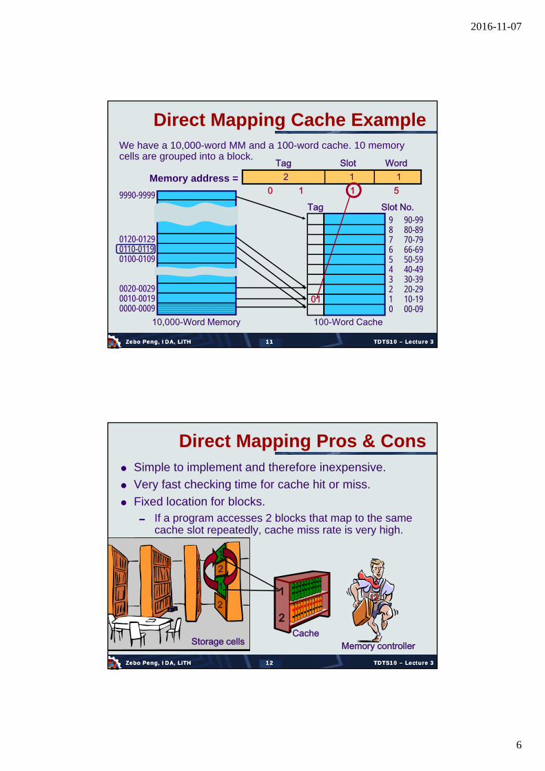
Direct Mapping Pros & Cons Simple to implement and therefore inexpensive.
Very fast checking time for cache hit or miss.
Fixed location for blocks. If a program accesses 2 blocks that map to the same
cache slot repeatedly, cache miss rate is very high.
Storage cells Memory controllerCache
1
2
12
1
2
2016-11-07
7
1313Zebo Peng, IDA, LiTHZebo Peng, IDA, LiTH TDTS10 – Lecture 3TDTS10 – Lecture 3
100-Word Cache
Tag (3 ps)90-9980-8970-7966-6950-5940-4930-3920-2910-1900-09
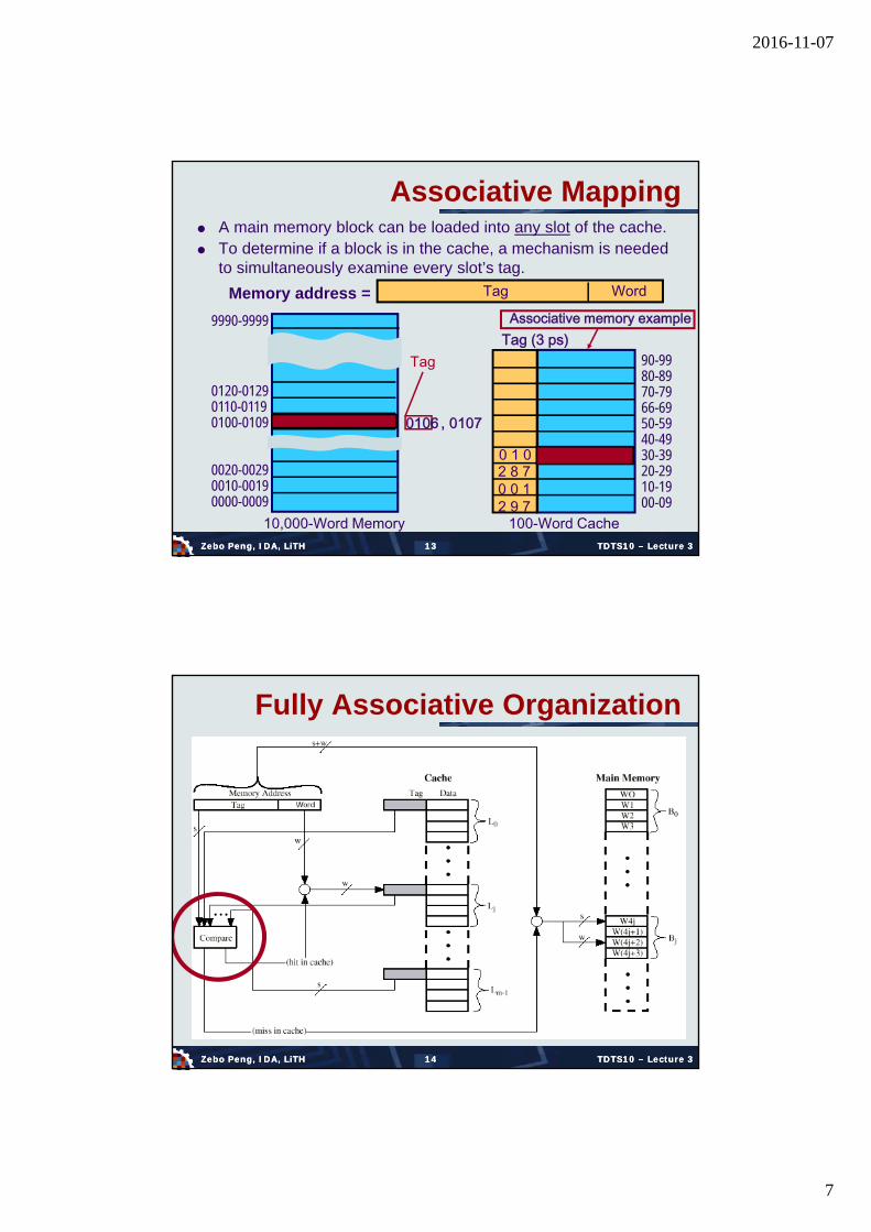
Associative Mapping A main memory block can be loaded into any slot of the cache. To determine if a block is in the cache, a mechanism is needed
to simultaneously examine every slot’s tag.
0020-00290010-00190000-0009
9990-9999
0120-01290110-01190100-0109
10,000-Word Memory
Tag
0 1 02 8 70 0 12 9 7
0106
Associative memory example
, 0107
Memory address = Tag Word
1414Zebo Peng, IDA, LiTHZebo Peng, IDA, LiTH TDTS10 – Lecture 3TDTS10 – Lecture 3
Fully Associative Organization
2016-11-07
8
1515Zebo Peng, IDA, LiTHZebo Peng, IDA, LiTH TDTS10 – Lecture 3TDTS10 – Lecture 3
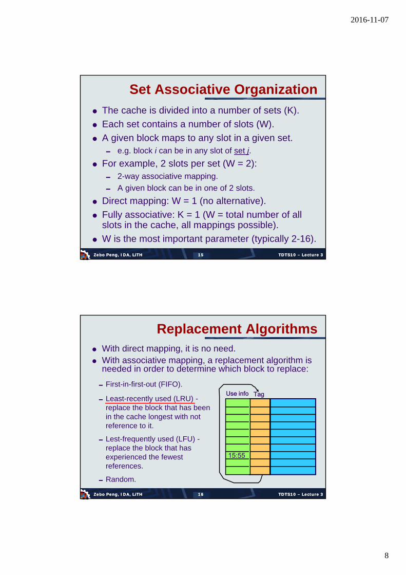
Set Associative Organization
The cache is divided into a number of sets (K).
Each set contains a number of slots (W).
A given block maps to any slot in a given set. e.g. block i can be in any slot of set j.
For example, 2 slots per set (W = 2): 2-way associative mapping.
A given block can be in one of 2 slots.
Direct mapping: W = 1 (no alternative).
Fully associative: K = 1 (W = total number of all slots in the cache, all mappings possible).
W is the most important parameter (typically 2-16).
1616Zebo Peng, IDA, LiTHZebo Peng, IDA, LiTH TDTS10 – Lecture 3TDTS10 – Lecture 3
Replacement Algorithms With direct mapping, it is no need. With associative mapping, a replacement algorithm is
needed in order to determine which block to replace:
First-in-first-out (FIFO).TagUse info
Least-recently used (LRU) -replace the block that has been in the cache longest with not reference to it.
Lest-frequently used (LFU) -replace the block that has experienced the fewest references.
Random.
15:55
2016-11-07
9
1717Zebo Peng, IDA, LiTHZebo Peng, IDA, LiTH TDTS10 – Lecture 3TDTS10 – Lecture 3
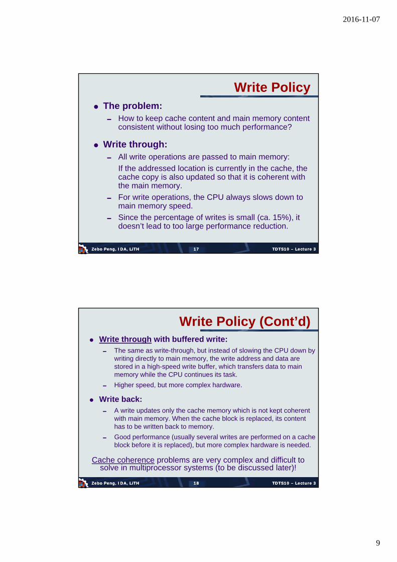
Write Policy The problem: How to keep cache content and main memory content
consistent without losing too much performance?
Write through: All write operations are passed to main memory:
If the addressed location is currently in the cache, the cache copy is also updated so that it is coherent with the main memory.
For write operations, the CPU always slows down to main memory speed.
Since the percentage of writes is small (ca. 15%), it doesn’t lead to too large performance reduction.
1818Zebo Peng, IDA, LiTHZebo Peng, IDA, LiTH TDTS10 – Lecture 3TDTS10 – Lecture 3
Write Policy (Cont’d) Write through with buffered write:
The same as write-through, but instead of slowing the CPU down by writing directly to main memory, the write address and data are stored in a high-speed write buffer, which transfers data to main memory while the CPU continues its task.
Higher speed, but more complex hardware.
Write back: A write updates only the cache memory which is not kept coherent
with main memory. When the cache block is replaced, its content has to be written back to memory.
Good performance (usually several writes are performed on a cache block before it is replaced), but more complex hardware is needed.
Cache coherence problems are very complex and difficult to solve in multiprocessor systems (to be discussed later)!
2016-11-07
10
1919Zebo Peng, IDA, LiTHZebo Peng, IDA, LiTH TDTS10 – Lecture 3TDTS10 – Lecture 3
Cache Architecture Examples Intel Pentium (introduced first in1993)
Two on-chip caches, one for data and one for instructions. Each cache: 8 KB. Line size: 32 bytes. 2-way set associative organization.
AMD Opteron 140 (introduced 2003) Two L1 cache: one for instruction and one for data; 64 KB each. 2-way associative organization. L2 cache: 1 MB, 16-way associative organization.
ARM Cortex-A15 (introduced 2012) Each core has separate L1 data and instruction caches. 64 KB (32 KB I-cache, 32 KB D-cache) per core. L2 cache, unified and common for all cores, up to 4 MB.
2020Zebo Peng, IDA, LiTHZebo Peng, IDA, LiTH TDTS10 – Lecture 3TDTS10 – Lecture 3
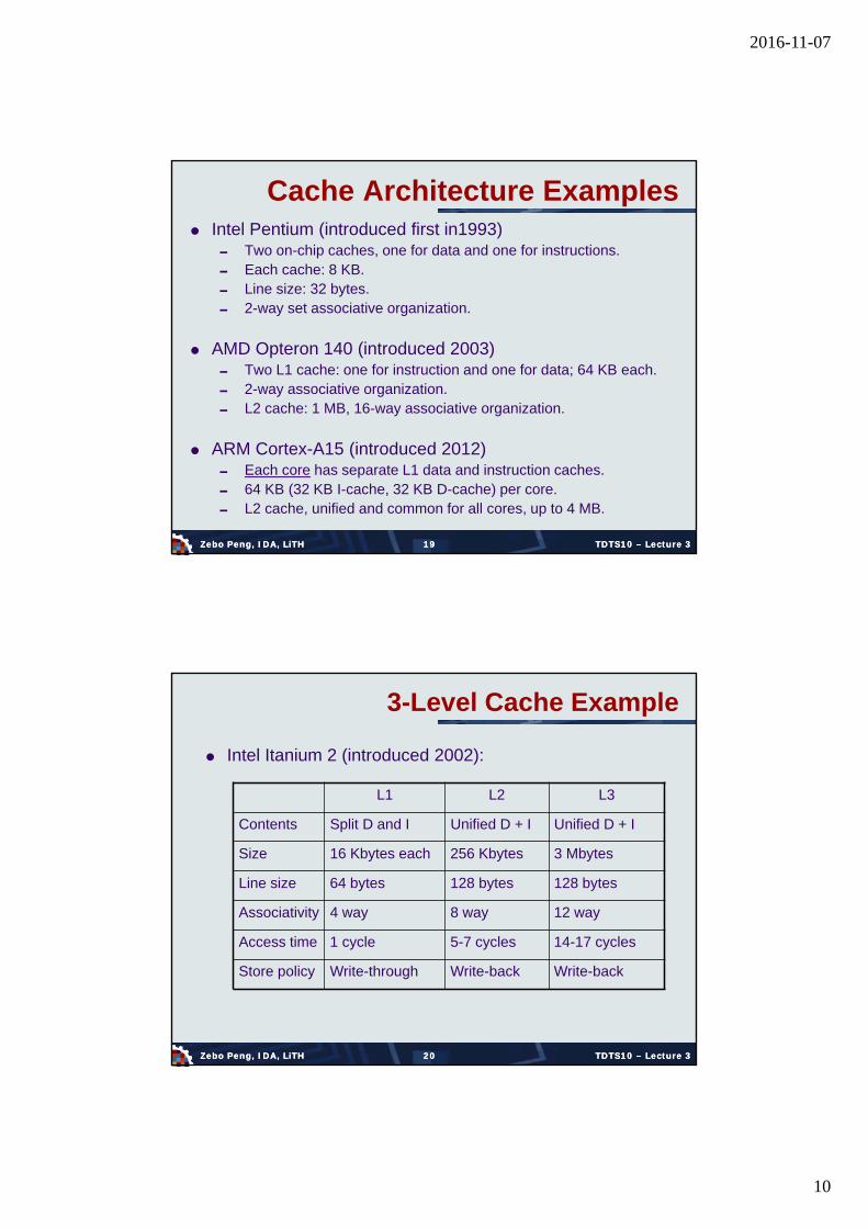
3-Level Cache Example
L1 L2 L3
Contents Split D and I Unified D + I Unified D + I
Size 16 Kbytes each 256 Kbytes 3 Mbytes
Line size 64 bytes 128 bytes 128 bytes
Associativity 4 way 8 way 12 way
Access time 1 cycle 5-7 cycles 14-17 cycles
Store policy Write-through Write-back Write-back
Intel Itanium 2 (introduced 2002):
2016-11-07
11
2121Zebo Peng, IDA, LiTHZebo Peng, IDA, LiTH TDTS10 – Lecture 3TDTS10 – Lecture 3
Lecture 3: Cache & I/O
Virtual memory
Cache memory
I/O operations
2222Zebo Peng, IDA, LiTHZebo Peng, IDA, LiTH TDTS10 – Lecture 3TDTS10 – Lecture 3
Motivation for Virtual Memory
The physical main memory (RAM) is relatively limited in capacity.
It may not be big enough to store all the executing programs at the same time.
A program may need memory larger than the main memory size, but the whole program doesn’t need to be kept in the main memory at the same time.
Virtual Memory takes advantage of the fact that at any given instant of time, an executing program needs only a fraction of the memory that the whole program occupies.
The basic idea: Load only pieces of each executing program which are currently needed (on demand).
2016-11-07
12
2323Zebo Peng, IDA, LiTHZebo Peng, IDA, LiTH TDTS10 – Lecture 3TDTS10 – Lecture 3
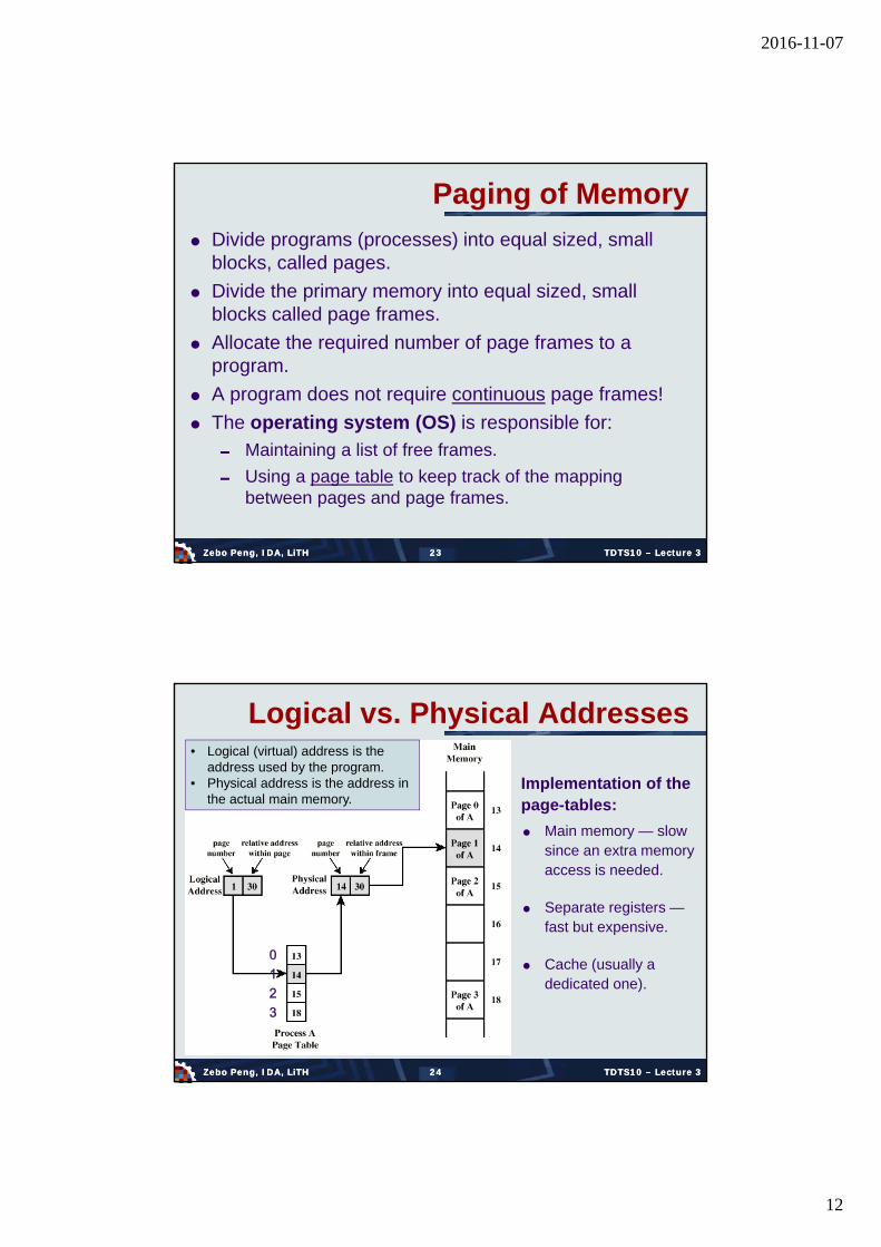
Paging of Memory
Divide programs (processes) into equal sized, small blocks, called pages.
Divide the primary memory into equal sized, small blocks called page frames.
Allocate the required number of page frames to a program.
A program does not require continuous page frames!
The operating system (OS) is responsible for:
Maintaining a list of free frames.
Using a page table to keep track of the mapping between pages and page frames.
2424Zebo Peng, IDA, LiTHZebo Peng, IDA, LiTH TDTS10 – Lecture 3TDTS10 – Lecture 3
Logical vs. Physical Addresses
Implementation of the page-tables:
Main memory — slow since an extra memory access is needed.
Separate registers —fast but expensive.
Cache (usually a dedicated one).
0123
• Logical (virtual) address is the address used by the program.
• Physical address is the address in the actual main memory.
2016-11-07
13
2525Zebo Peng, IDA, LiTHZebo Peng, IDA, LiTH TDTS10 – Lecture 3TDTS10 – Lecture 3
Motivation for Virtual Memory I
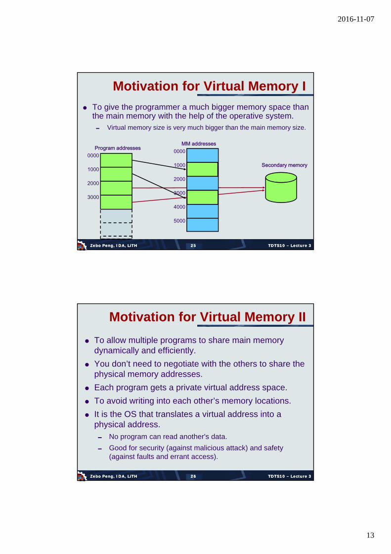
To give the programmer a much bigger memory space than the main memory with the help of the operative system. Virtual memory size is very much bigger than the main memory size.
0000
1000
2000
3000
Program addresses
Secondary memory
0000
1000
2000
3000
4000
5000
MM addresses
2626Zebo Peng, IDA, LiTHZebo Peng, IDA, LiTH TDTS10 – Lecture 3TDTS10 – Lecture 3
Motivation for Virtual Memory II
To allow multiple programs to share main memory dynamically and efficiently.
You don’t need to negotiate with the others to share the physical memory addresses.
Each program gets a private virtual address space.
To avoid writing into each other’s memory locations.
It is the OS that translates a virtual address into a physical address. No program can read another's data.
Good for security (against malicious attack) and safety (against faults and errant access).
2016-11-07
14
2727Zebo Peng, IDA, LiTHZebo Peng, IDA, LiTH TDTS10 – Lecture 3TDTS10 – Lecture 3
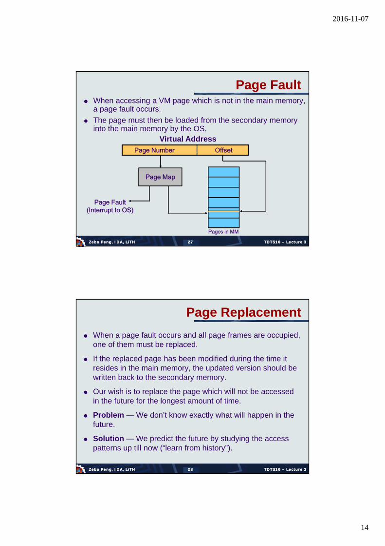
Page Fault When accessing a VM page which is not in the main memory,
a page fault occurs.
The page must then be loaded from the secondary memory into the main memory by the OS.
Virtual Address Page Number Offset
Page Map
Pages in MM
Page Fault(Interrupt to OS)
2828Zebo Peng, IDA, LiTHZebo Peng, IDA, LiTH TDTS10 – Lecture 3TDTS10 – Lecture 3
Page Replacement
When a page fault occurs and all page frames are occupied, one of them must be replaced.
If the replaced page has been modified during the time it resides in the main memory, the updated version should be written back to the secondary memory.
Our wish is to replace the page which will not be accessed in the future for the longest amount of time.
Problem — We don’t know exactly what will happen in the future.
Solution — We predict the future by studying the access patterns up till now (“learn from history”).

2016-11-07
15
2929Zebo Peng, IDA, LiTHZebo Peng, IDA, LiTH TDTS10 – Lecture 3TDTS10 – Lecture 3
Replacement Algorithms
FIFO (First In First Out) — To replace the one in MM the longest of time.
LRU (Least Recently Used) — To replace the one that has not be accessed the longest time.
LFU (Least Frequently Used) — To replace the one that has the smallest number of access during the latest time period.
The replacement by random technique (used for Cache)
is not used for VM!
3030Zebo Peng, IDA, LiTHZebo Peng, IDA, LiTH TDTS10 – Lecture 3TDTS10 – Lecture 3
Lecture 3: Cache & I/O
Virtual memory
Cache memory
I/O operations
2016-11-07
16
3131Zebo Peng, IDA, LiTHZebo Peng, IDA, LiTH TDTS10 – Lecture 3TDTS10 – Lecture 3
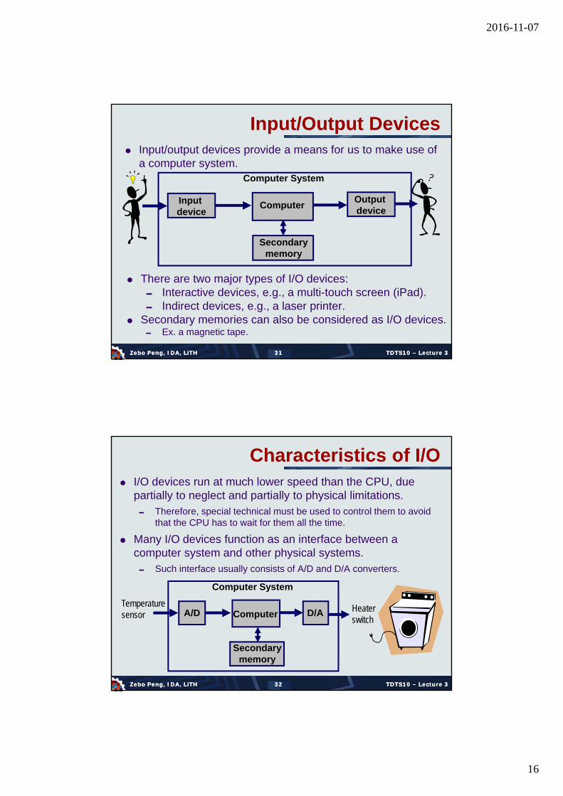
Input/Output Devices Input/output devices provide a means for us to make use of
a computer system.
Computer
Secondarymemory
Computer System
Input device
Output device
There are two major types of I/O devices: Interactive devices, e.g., a multi-touch screen (iPad). Indirect devices, e.g., a laser printer.
Secondary memories can also be considered as I/O devices. Ex. a magnetic tape.
3232Zebo Peng, IDA, LiTHZebo Peng, IDA, LiTH TDTS10 – Lecture 3TDTS10 – Lecture 3
Characteristics of I/O I/O devices run at much lower speed than the CPU, due
partially to neglect and partially to physical limitations. Therefore, special technical must be used to control them to avoid
that the CPU has to wait for them all the time.
Many I/O devices function as an interface between a computer system and other physical systems. Such interface usually consists of A/D and D/A converters.
Temperaturesensor
Heaterswitch
Computer
Secondarymemory
Computer System
A/D D/A

2016-11-07
17
3333Zebo Peng, IDA, LiTHZebo Peng, IDA, LiTH TDTS10 – Lecture 3TDTS10 – Lecture 3
An I/O Module Responsible for the control of one or several devices,
and the exchange of data between the devices and the main memory and/or CPU registers.
CPU
MM
3434Zebo Peng, IDA, LiTHZebo Peng, IDA, LiTH TDTS10 – Lecture 3TDTS10 – Lecture 3
Functions of an I/O Module
CPU
MM
Control and timing
CPU communication
Device communication
Data buffering
Error detection and correction

2016-11-07
18
3535Zebo Peng, IDA, LiTHZebo Peng, IDA, LiTH TDTS10 – Lecture 3TDTS10 – Lecture 3
Control of I/O Devices (1) Programmed I/O
The operations are controlled by I/O instructions, for example, READ and WRITE.
The instructions specify:• the particular I/O operation to perform; and
• the given device by giving its address (its ID number).
The CPU will wait for the I/O operation to be finished before it executes the next instruction.
Since the I/O devices are very slow, the CPU has to wait all the time instead of doing useful work.
It is a very simple but not an efficient method.
• can be used in an embedded system.
3636Zebo Peng, IDA, LiTHZebo Peng, IDA, LiTH TDTS10 – Lecture 3TDTS10 – Lecture 3
Programmed I/O Example
Select I/O device
Send data to thedevice interface
Check device status
Next instruction
Ready?
yes
no
Execution flow of aWRITE instruction(e.g. WRITE ‘P’, O1):
Start
The CPU does polling, or busy waiting.
The I/O device sets appropriate bits in the I/O status register.

2016-11-07
19
3737Zebo Peng, IDA, LiTHZebo Peng, IDA, LiTH TDTS10 – Lecture 3TDTS10 – Lecture 3
Control of I/O Devices (2)
Interrupt-driven I/O After the CPU sends an initialization signal to an I/O
device, it continues with the execution of programs.
When the I/O device is ready, or wants to get the attention of the CPU, it sends an interrupt signal to the CPU.
When the CPU receives an interrupt signal, it will first finish the execution of the current instruction and then execute the interrupt service routine (ISR).
This mechanism is used to free the CPU from having to check periodically (polling) the I/O devices to see it they are in need of any attention.
3838Zebo Peng, IDA, LiTHZebo Peng, IDA, LiTH TDTS10 – Lecture 3TDTS10 – Lecture 3
Interrupt Service Routine (ISR) Save all status information which is needed to resume
execution of the current sequence of instructions. Put the saved PC value in a safe place!
Deal with the interrupt, for example, by reading data from the input device.
Restore the saved status information and then resume execution of the interrupted program.
current sequence
interrupt
interrupt routine
original sequence resumed

2016-11-07
20
3939Zebo Peng, IDA, LiTHZebo Peng, IDA, LiTH TDTS10 – Lecture 3TDTS10 – Lecture 3
Instruction Cycle w. Interrupts
Fetch nextinstruction
Executeinstruction
Check for interrupt
Start
Stop
Fetch cycle
Execute cycle
Interrupt cycle
Interrupts enabledInterrupts disabled
HW: Save the current PC value &set PC as the 1st address of ISR
4040Zebo Peng, IDA, LiTHZebo Peng, IDA, LiTH TDTS10 – Lecture 3TDTS10 – Lecture 3
Multiple Interrupts A new interrupt may occur while the current interrupt is
being processed (execution of the ISR instructions). Disabled interrupt approach: CPU ignores new interrupt
signals while processing an interrupt.
Priority-based approach: An interrupt of higher priority will interrupt the processing of a lower-priority interrupt.
current sequence
interrupt routine
original sequence resumedinterrupt
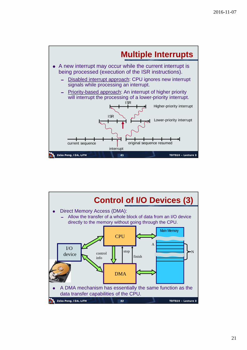
2016-11-07
21
4141Zebo Peng, IDA, LiTHZebo Peng, IDA, LiTH TDTS10 – Lecture 3TDTS10 – Lecture 3
current sequence original sequence resumedinterrupt
ISRLower-priority interrupt
Multiple Interrupts A new interrupt may occur while the current interrupt is
being processed (execution of the ISR instructions). Disabled interrupt approach: CPU ignores new interrupt
signals while processing an interrupt.
Priority-based approach: An interrupt of higher priority will interrupt the processing of a lower-priority interrupt.
ISRHigher-priority interrupt
4242Zebo Peng, IDA, LiTHZebo Peng, IDA, LiTH TDTS10 – Lecture 3TDTS10 – Lecture 3
Direct Memory Access (DMA): Allow the transfer of a whole block of data from an I/O device
directly to the memory without going through the CPU.
N
CPU
I/O device
A
Main Memory
controlinfo
stop
finish
DMA
Control of I/O Devices (3)
A DMA mechanism has essentially the same function as the data transfer capabilities of the CPU.
2016-11-07
22
4343Zebo Peng, IDA, LiTHZebo Peng, IDA, LiTH TDTS10 – Lecture 3TDTS10 – Lecture 3
I/O Operation Summary
Data exchanges of a computer system with the outside world are provided by the I/O devices.
Secondary memories can also be considered as I/O devices.
Since computers deal with many different types of users and interface also with many different physical systems, there is a large variety of I/O devices.
We need different techniques to control the I/O devices, due to the large differences between I/O operations.
The I/O function is usually the most unreliable part of a computer system, and we need techniques for error detection and recovery.


![Cache Memory - Trinity College Dublin caches.pdf · update cache line and main memory write miss update main memory ONLY [non write allocate cache] OR select a cache line [using replacement](https://static.fdocuments.in/doc/165x107/5ecffe5cdf7e6609157f3520/cache-memory-trinity-college-dublin-cachespdf-update-cache-line-and-main-memory.jpg)