
Lecture 20: Introduction to semiconductor manufacturingLecture 20: Introduction to semiconductor...
17
Lecture 20: Introduction to semiconductor manufacturing Contents 1 Introduction 1 2 Integrated circuits 5 3 Device miniaturization 7 4 Challenges in IC manufacturing 11 5 IC manufacturing stages 17 1 Introduction There are a wide variety of electronic devices starting with the simple pn junction diodes, transistors, and extending into opto-electronic devices like LEDs, lasers, and solar cells. These are made from a variety of semiconduc- tor materials though silicon is the dominant material in the micro electronics industry. Other semiconductors are used, especially for optical devices, since silicon is an indirect band gap material. How these devices are manufactured and assembled to form useful devices, like computers, tablets, cell phones, and a host of other microelectronic devices is a critical part of the industry. This is especially important, since, with increased miniaturization, devices are becoming smaller and have greater functionality. Other form factors like battery life, operating power, heat generation and dissipation, also become critical, especially for mobile computing. Understanding the various steps behind fabrication of these devices is important to understand the challenges facing the semiconductor industry. The first electronic device invented was the vacuum tube, by Lee Deforest in 1906. This was the triode, called audion, and the schematic of the device 1
Transcript of Lecture 20: Introduction to semiconductor manufacturingLecture 20: Introduction to semiconductor...
Lecture 20: Introduction tosemiconductor manufacturing
Contents
1 Introduction 1
2 Integrated circuits 5
3 Device miniaturization 7
4 Challenges in IC manufacturing 11
5 IC manufacturing stages 17
1 Introduction
There are a wide variety of electronic devices starting with the simple pnjunction diodes, transistors, and extending into opto-electronic devices likeLEDs, lasers, and solar cells. These are made from a variety of semiconduc-tor materials though silicon is the dominant material in the micro electronicsindustry. Other semiconductors are used, especially for optical devices, sincesilicon is an indirect band gap material. How these devices are manufacturedand assembled to form useful devices, like computers, tablets, cell phones,and a host of other microelectronic devices is a critical part of the industry.This is especially important, since, with increased miniaturization, devicesare becoming smaller and have greater functionality. Other form factors likebattery life, operating power, heat generation and dissipation, also becomecritical, especially for mobile computing. Understanding the various stepsbehind fabrication of these devices is important to understand the challengesfacing the semiconductor industry.The first electronic device invented was the vacuum tube, by Lee Deforestin 1906. This was the triode, called audion, and the schematic of the device
1
MM5017: Electronic materials, devices, and fabrication
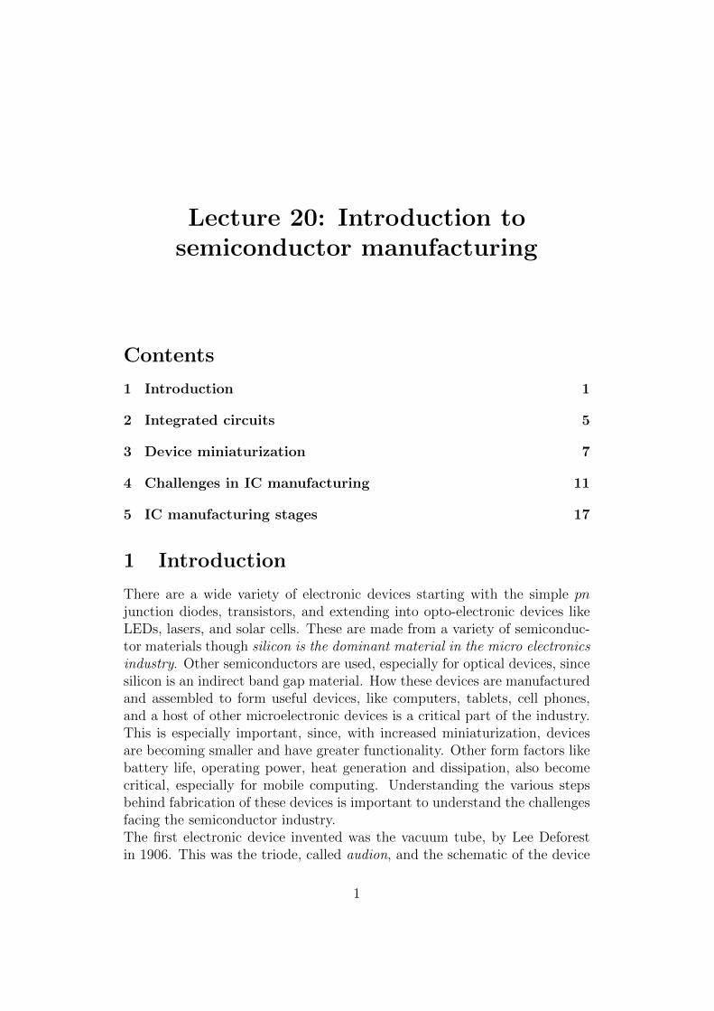
Figure 1: Schematic of the vacuum tube (a) triode and (b) diode. Sourceshttp://en.wikipedia.org/wiki/Triode and http://en.wikipedia.org/wiki/Diode
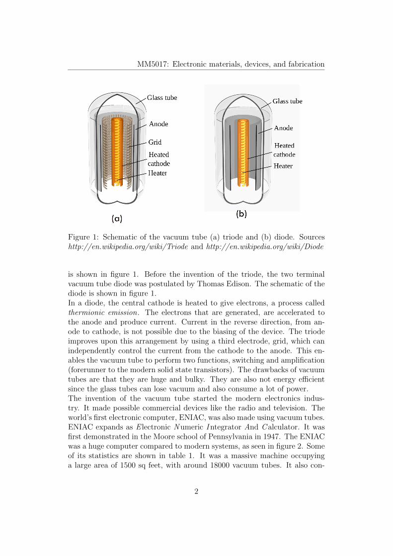
is shown in figure 1. Before the invention of the triode, the two terminalvacuum tube diode was postulated by Thomas Edison. The schematic of thediode is shown in figure 1.In a diode, the central cathode is heated to give electrons, a process calledthermionic emission. The electrons that are generated, are accelerated tothe anode and produce current. Current in the reverse direction, from an-ode to cathode, is not possible due to the biasing of the device. The triodeimproves upon this arrangement by using a third electrode, grid, which canindependently control the current from the cathode to the anode. This en-ables the vacuum tube to perform two functions, switching and amplification(forerunner to the modern solid state transistors). The drawbacks of vacuumtubes are that they are huge and bulky. They are also not energy efficientsince the glass tubes can lose vacuum and also consume a lot of power.The invention of the vacuum tube started the modern electronics indus-try. It made possible commercial devices like the radio and television. Theworld’s first electronic computer, ENIAC, was also made using vacuum tubes.ENIAC expands as E lectronic N umeric I ntegrator And C alculator. It wasfirst demonstrated in the Moore school of Pennsylvania in 1947. The ENIACwas a huge computer compared to modern systems, as seen in figure 2. Someof its statistics are shown in table 1. It was a massive machine occupyinga large area of 1500 sq feet, with around 18000 vacuum tubes. It also con-
2
MM5017: Electronic materials, devices, and fabrication
Figure 2: Two programmers operating the ENIAC. Typical statistics of thecomputer are listed in table 1. Source http://en.wikipedia.org/wiki/ENIAC
Table 1: Some typical statistics of the ENIAC. Compared to the moderncomputer, it was a massive machine. SourceMicrochip fabrication - Petervan Zant.
Size, ft 30 × 50Weight, tons 30
Vacuum tubes, nos. 18,000Resistors, nos 70,000
Capacitors, nos 10,000Switches, nos 6000
Power requirement, W 150,000Cost (in 1940) $ 400,000
3
MM5017: Electronic materials, devices, and fabrication
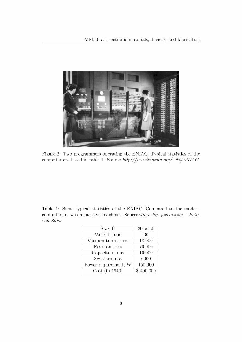
Figure 3: Schematic of the first transistor developed in Bell labs. Adaptedfrom Microchip fabrication - Peter van Zant.
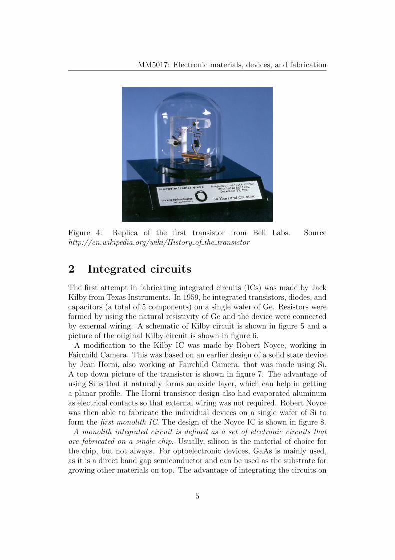
sumed a large amount of power and consequently generated a lot of heat.This made it highly unreliable with the longest operating period, withoutany vacuum tube failure, of 5 days (around 116 hours). The large size andpoor performance of the ENIAC was due to the presence of vacuum tubes,which had to individually wired to achieve the desired performance. For anysize reduction the triode size had to be reduced. This was made possibleby the development of the modern solid state transistor, which started therevolution in micro electronics.The first solid state based triode i.e. the transistor was invented in Bell Labsin 1947. It was invented by John Bardeen, William Schokley, and WalterBrattain. The device was an electrical amplifier based on germanium, shownin figure 3. The device functioned similar to the vacuum tube triode, but wassmaller, lighter, and had a much lower power requirement. A replica of thefirst transistor is shown in figure 4. The inventors of the solid state transistorwon the Nobel prize in Physics for their work in 1956. John Bardeen thenmoved to University of Illinois at Urbana-Champaign where he won a sec-ond Nobel prize in Physics in 1972 for his work with Leon Cooper and JohnSchrieffer on a theory of superconductivity (BCS theory). Thus, he becamethe only person to win two Nobel prizes in Physics.The invention of the transistor started the era of solid state devices. Discreteelectrical components like transistors, diodes, capacitors, and resistors canbe fabricated and then joined to form the required device. While these werestill smaller than vacuum tube devices, true miniaturization could only beachieved by integrating the various devices in one wafer.
4
MM5017: Electronic materials, devices, and fabrication
Figure 4: Replica of the first transistor from Bell Labs. Sourcehttp://en.wikipedia.org/wiki/History of the transistor
2 Integrated circuits
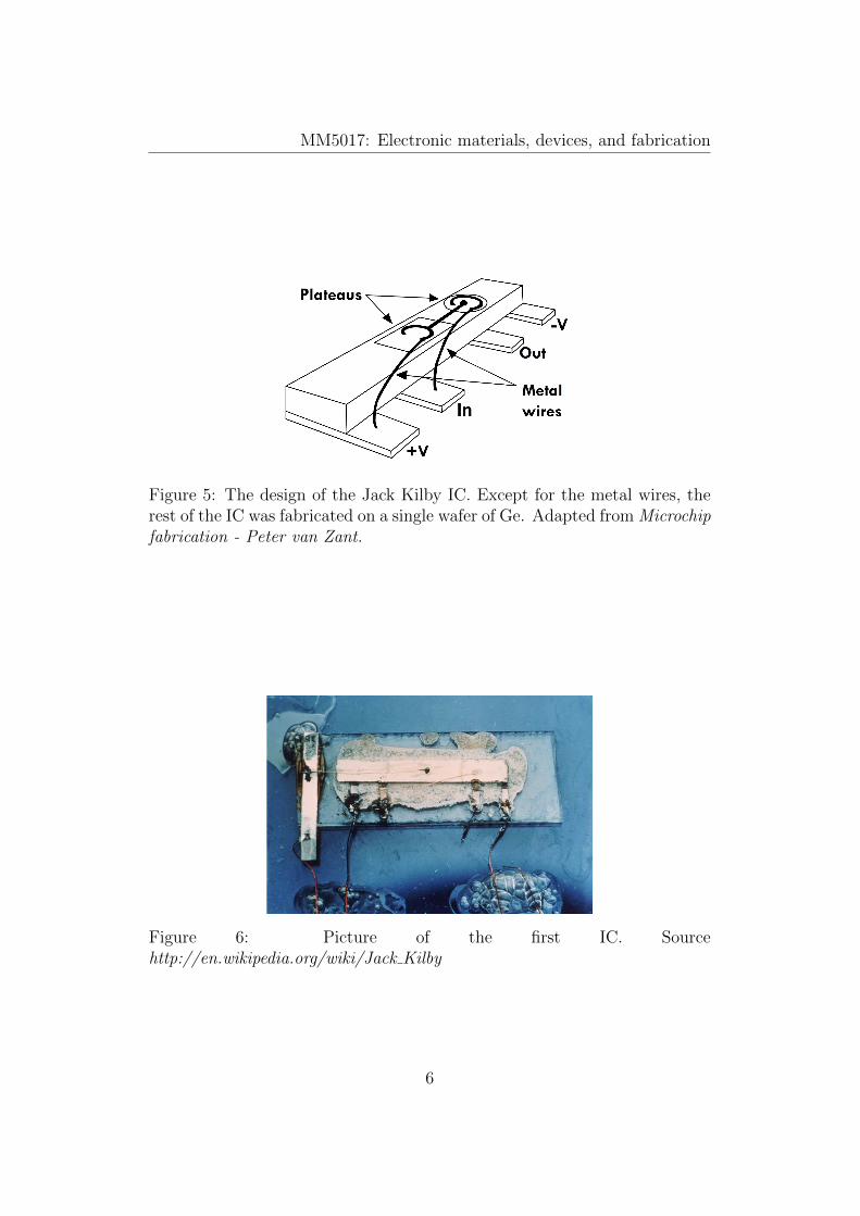
The first attempt in fabricating integrated circuits (ICs) was made by JackKilby from Texas Instruments. In 1959, he integrated transistors, diodes, andcapacitors (a total of 5 components) on a single wafer of Ge. Resistors wereformed by using the natural resistivity of Ge and the device were connectedby external wiring. A schematic of Kilby circuit is shown in figure 5 and apicture of the original Kilby circuit is shown in figure 6.
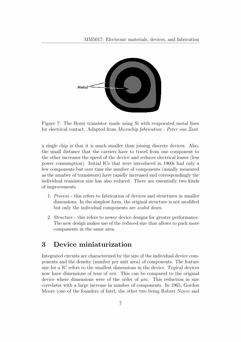
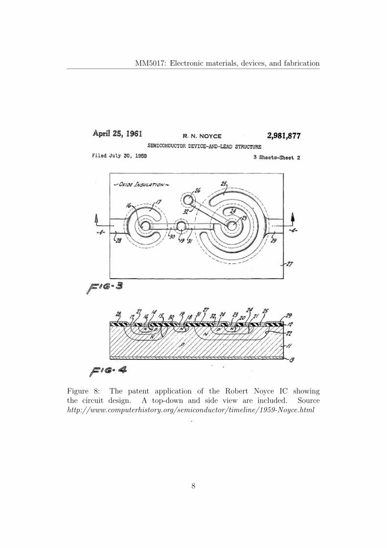
A modification to the Kilby IC was made by Robert Noyce, working inFairchild Camera. This was based on an earlier design of a solid state deviceby Jean Horni, also working at Fairchild Camera, that was made using Si.A top down picture of the transistor is shown in figure 7. The advantage ofusing Si is that it naturally forms an oxide layer, which can help in gettinga planar profile. The Horni transistor design also had evaporated aluminumas electrical contacts so that external wiring was not required. Robert Noycewas then able to fabricate the individual devices on a single wafer of Si toform the first monolith IC. The design of the Noyce IC is shown in figure 8.
A monolith integrated circuit is defined as a set of electronic circuits thatare fabricated on a single chip. Usually, silicon is the material of choice forthe chip, but not always. For optoelectronic devices, GaAs is mainly used,as it is a direct band gap semiconductor and can be used as the substrate forgrowing other materials on top. The advantage of integrating the circuits on
5
MM5017: Electronic materials, devices, and fabrication
Figure 5: The design of the Jack Kilby IC. Except for the metal wires, therest of the IC was fabricated on a single wafer of Ge. Adapted from Microchipfabrication - Peter van Zant.
Figure 6: Picture of the first IC. Sourcehttp://en.wikipedia.org/wiki/Jack Kilby
6
MM5017: Electronic materials, devices, and fabrication
Figure 7: The Horni transistor made using Si with evaporated metal linesfor electrical contact. Adapted from Microchip fabrication - Peter van Zant.
a single chip is that it is much smaller than joining discrete devices. Also,the small distance that the carriers have to travel from one component tothe other increases the speed of the device and reduces electrical losses (lesspower consumption). Initial ICs that were introduced in 1960s had only afew components but over time the number of components (usually measuredas the number of transistors) have rapidly increased and correspondingly theindividual transistor size has also reduced. There are essentially two kindsof improvements
1. Process - this refers to fabrication of devices and structures in smallerdimensions. In the simplest form, the original structure is not modifiedbut only the individual components are scaled down.
2. Structure - this refers to newer device designs for greater performance.The new design makes use of the reduced size that allows to pack morecomponents in the same area.
3 Device miniaturization
Integrated circuits are characterized by the size of the individual device com-ponents and the density (number per unit area) of components. The featuresize for a IC refers to the smallest dimensions in the device. Typical devicesnow have dimensions of tens of nm. This can be compared to the originaldevice where dimensions were of the order of µm. This reduction in sizecorrelates with a large increase in number of components. In 1965, GordonMoore (one of the founders of Intel, the other two being Robert Noyce and
7
MM5017: Electronic materials, devices, and fabrication
Figure 8: The patent application of the Robert Noyce IC showingthe circuit design. A top-down and side view are included. Sourcehttp://www.computerhistory.org/semiconductor/timeline/1959-Noyce.html
.
8
MM5017: Electronic materials, devices, and fabrication
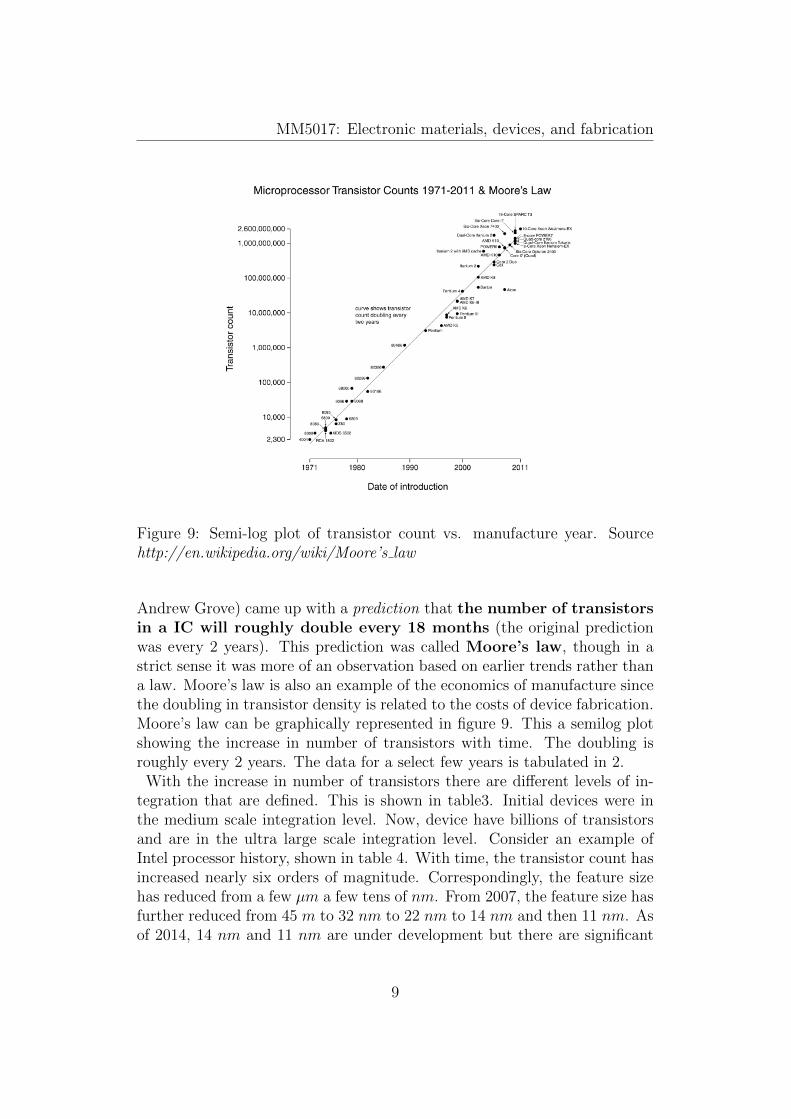
Figure 9: Semi-log plot of transistor count vs. manufacture year. Sourcehttp://en.wikipedia.org/wiki/Moore’s law
Andrew Grove) came up with a prediction that the number of transistorsin a IC will roughly double every 18 months (the original predictionwas every 2 years). This prediction was called Moore’s law, though in astrict sense it was more of an observation based on earlier trends rather thana law. Moore’s law is also an example of the economics of manufacture sincethe doubling in transistor density is related to the costs of device fabrication.Moore’s law can be graphically represented in figure 9. This a semilog plotshowing the increase in number of transistors with time. The doubling isroughly every 2 years. The data for a select few years is tabulated in 2.
With the increase in number of transistors there are different levels of in-tegration that are defined. This is shown in table3. Initial devices were inthe medium scale integration level. Now, device have billions of transistorsand are in the ultra large scale integration level. Consider an example ofIntel processor history, shown in table 4. With time, the transistor count hasincreased nearly six orders of magnitude. Correspondingly, the feature sizehas reduced from a few µm a few tens of nm. From 2007, the feature size hasfurther reduced from 45 m to 32 nm to 22 nm to 14 nm and then 11 nm. Asof 2014, 14 nm and 11 nm are under development but there are significant
9
MM5017: Electronic materials, devices, and fabrication
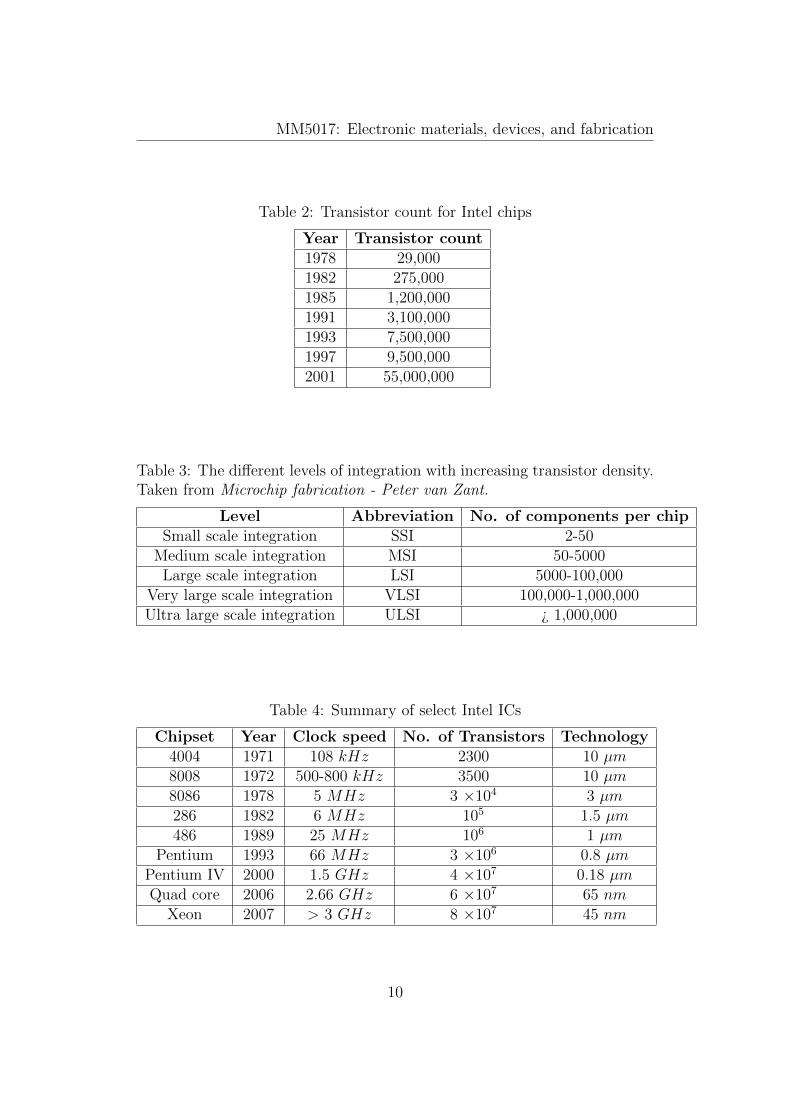
Table 2: Transistor count for Intel chips
Year Transistor count1978 29,0001982 275,0001985 1,200,0001991 3,100,0001993 7,500,0001997 9,500,0002001 55,000,000
Table 3: The different levels of integration with increasing transistor density.Taken from Microchip fabrication - Peter van Zant.
Level Abbreviation No. of components per chipSmall scale integration SSI 2-50
Medium scale integration MSI 50-5000Large scale integration LSI 5000-100,000
Very large scale integration VLSI 100,000-1,000,000Ultra large scale integration ULSI ¿ 1,000,000
Table 4: Summary of select Intel ICs
Chipset Year Clock speed No. of Transistors Technology4004 1971 108 kHz 2300 10 µm8008 1972 500-800 kHz 3500 10 µm8086 1978 5 MHz 3 ×10⁴ 3 µm286 1982 6 MHz 105 1.5 µm486 1989 25 MHz 106 1 µm
Pentium 1993 66 MHz 3 ×10⁶ 0.8 µmPentium IV 2000 1.5 GHz 4 ×10⁷ 0.18 µmQuad core 2006 2.66 GHz 6 ×10⁷ 65 nm
Xeon 2007 > 3 GHz 8 ×10⁷ 45 nm
10
MM5017: Electronic materials, devices, and fabrication
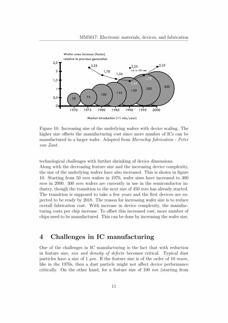
Figure 10: Increasing size of the underlying wafers with device scaling. Thehigher size offsets the manufacturing cost since more number of ICs can bemanufactured in a larger wafer. Adapted from Microchip fabrication - Petervan Zant.
technological challenges with further shrinking of device dimensions.Along with the decreasing feature size and the increasing device complexity,the size of the underlying wafers have also increased. This is shown in figure10. Starting from 50 mm wafers in 1970, wafer sizes have increased to 300mm in 2000. 300 mm wafers are currently in use in the semiconductor in-dustry, though the transition to the next size of 450 mm has already started.The transition is supposed to take a few years and the first devices are ex-pected to be ready by 2018. The reason for increasing wafer size is to reduceoverall fabrication cost. With increase in device complexity, the manufac-turing costs per chip increase. To offset this increased cost, more number ofchips need to be manufactured. This can be done by increasing the wafer size.
4 Challenges in IC manufacturing
One of the challenges in IC manufacturing is the fact that with reductionin feature size, size and density of defects becomes critical. Typical dustparticles have a size of 1 µm. If the feature size is of the order of 10 mum,like in the 1970s, then a dust particle might not affect device performancecritically. On the other hand, for a feature size of 100 nm (starting from
11
MM5017: Electronic materials, devices, and fabrication
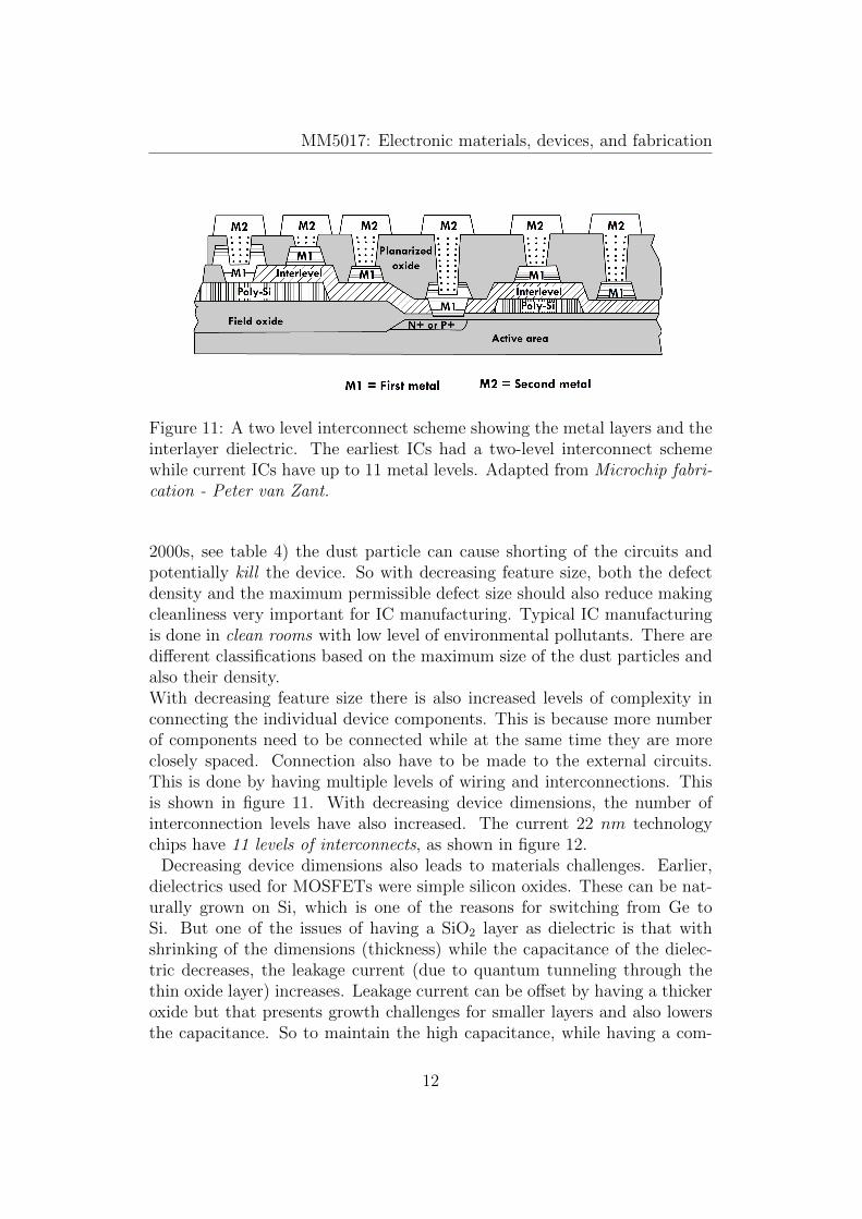
Figure 11: A two level interconnect scheme showing the metal layers and theinterlayer dielectric. The earliest ICs had a two-level interconnect schemewhile current ICs have up to 11 metal levels. Adapted from Microchip fabri-cation - Peter van Zant.
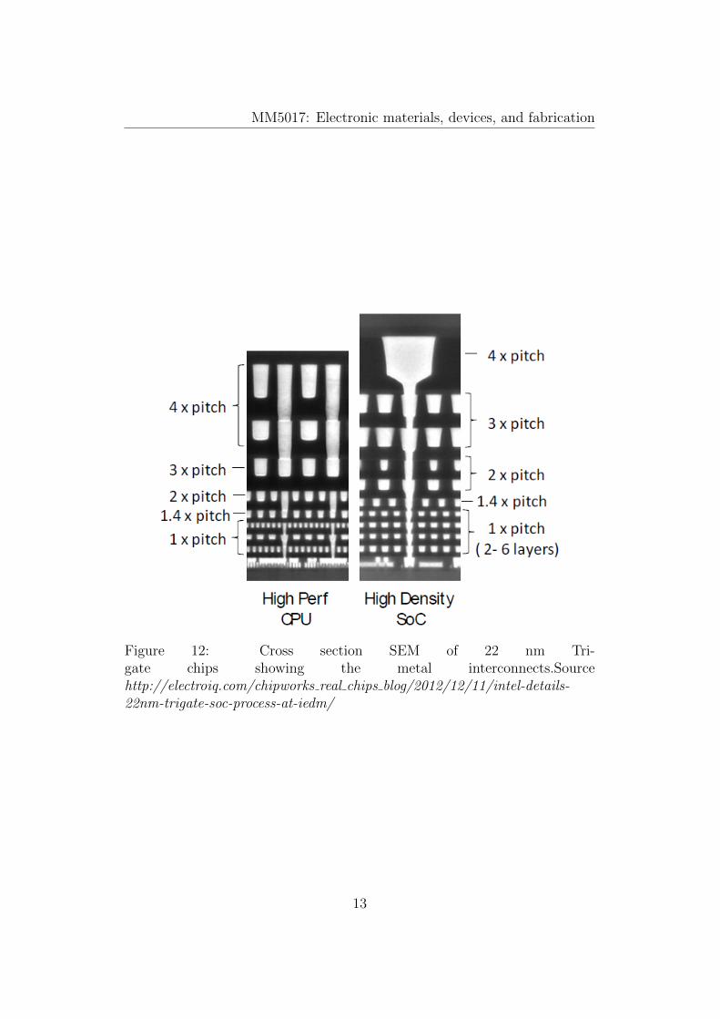
2000s, see table 4) the dust particle can cause shorting of the circuits andpotentially kill the device. So with decreasing feature size, both the defectdensity and the maximum permissible defect size should also reduce makingcleanliness very important for IC manufacturing. Typical IC manufacturingis done in clean rooms with low level of environmental pollutants. There aredifferent classifications based on the maximum size of the dust particles andalso their density.With decreasing feature size there is also increased levels of complexity inconnecting the individual device components. This is because more numberof components need to be connected while at the same time they are moreclosely spaced. Connection also have to be made to the external circuits.This is done by having multiple levels of wiring and interconnections. Thisis shown in figure 11. With decreasing device dimensions, the number ofinterconnection levels have also increased. The current 22 nm technologychips have 11 levels of interconnects, as shown in figure 12.
Decreasing device dimensions also leads to materials challenges. Earlier,dielectrics used for MOSFETs were simple silicon oxides. These can be nat-urally grown on Si, which is one of the reasons for switching from Ge toSi. But one of the issues of having a SiO2 layer as dielectric is that withshrinking of the dimensions (thickness) while the capacitance of the dielec-tric decreases, the leakage current (due to quantum tunneling through thethin oxide layer) increases. Leakage current can be offset by having a thickeroxide but that presents growth challenges for smaller layers and also lowersthe capacitance. So to maintain the high capacitance, while having a com-
12
MM5017: Electronic materials, devices, and fabrication
Figure 12: Cross section SEM of 22 nm Tri-gate chips showing the metal interconnects.Sourcehttp://electroiq.com/chipworks real chips blog/2012/12/11/intel-details-22nm-trigate-soc-process-at-iedm/
13
MM5017: Electronic materials, devices, and fabrication
Figure 13: Planar transistor showing the source, drain, and gate. There is aalso the dielectric layer and there is only one interface between the semicon-ductor and the gate. Source http://www.anandtech.com/show/4313/intel-announces-first-22nm-3d-trigate-transistors-shipping-in-2h-2011
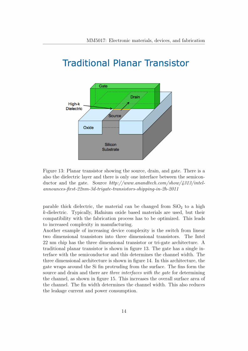
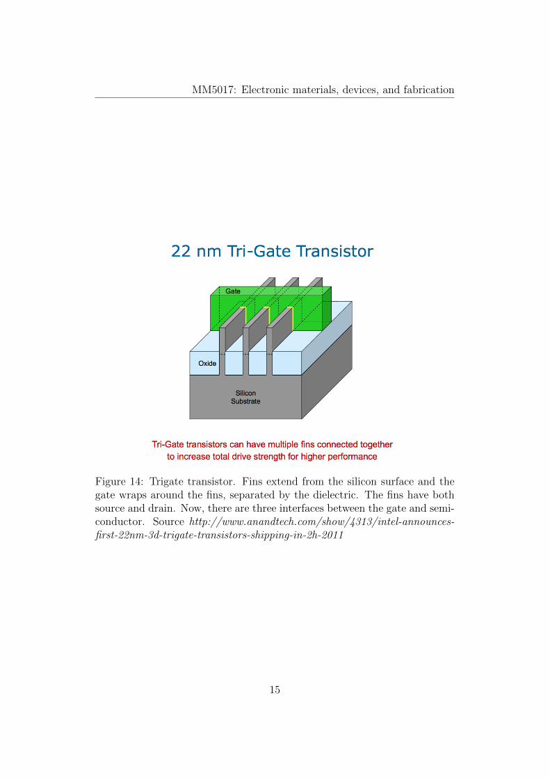
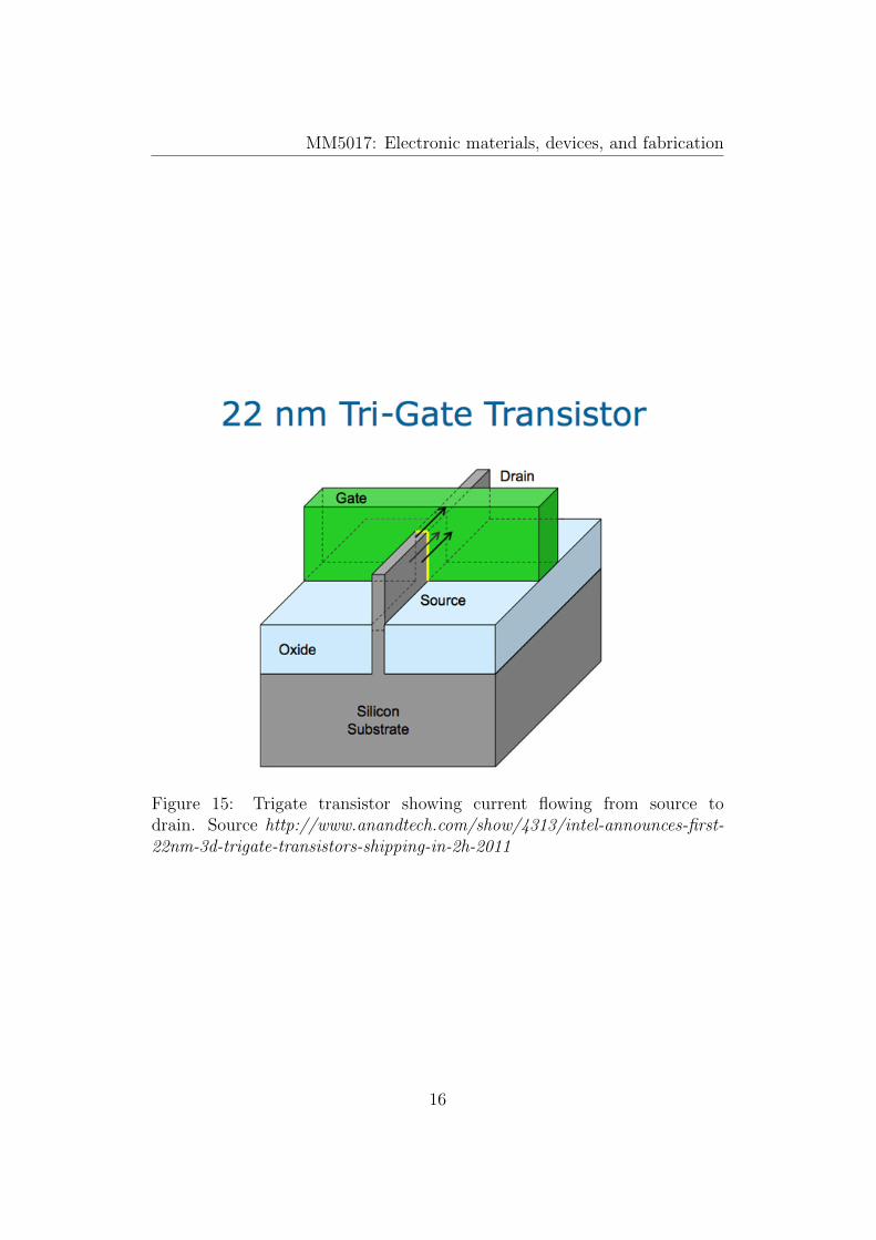
parable thick dielectric, the material can be changed from SiO2 to a highk-dielectric. Typically, Hafnium oxide based materials are used, but theircompatibility with the fabrication process has to be optimized. This leadsto increased complexity in manufacturing.Another example of increasing device complexity is the switch from lineartwo dimensional transistors into three dimensional transistors. The Intel22 nm chip has the three dimensional transistor or tri-gate architecture. Atraditional planar transistor is shown in figure 13. The gate has a single in-terface with the semiconductor and this determines the channel width. Thethree dimensional architecture is shown in figure 14. In this architecture, thegate wraps around the Si fin protruding from the surface. The fins form thesource and drain and there are three interfaces with the gate for determiningthe channel, as shown in figure 15. This increases the overall surface area ofthe channel. The fin width determines the channel width. This also reducesthe leakage current and power consumption.
14
MM5017: Electronic materials, devices, and fabrication
Figure 14: Trigate transistor. Fins extend from the silicon surface and thegate wraps around the fins, separated by the dielectric. The fins have bothsource and drain. Now, there are three interfaces between the gate and semi-conductor. Source http://www.anandtech.com/show/4313/intel-announces-first-22nm-3d-trigate-transistors-shipping-in-2h-2011
15
MM5017: Electronic materials, devices, and fabrication
Figure 15: Trigate transistor showing current flowing from source todrain. Source http://www.anandtech.com/show/4313/intel-announces-first-22nm-3d-trigate-transistors-shipping-in-2h-2011
16
MM5017: Electronic materials, devices, and fabrication
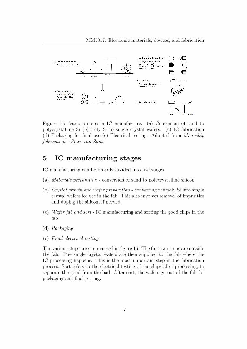
Figure 16: Various steps in IC manufacture. (a) Conversion of sand topolycrystalline Si (b) Poly Si to single crystal wafers. (c) IC fabrication(d) Packaging for final use (e) Electrical testing. Adapted from Microchipfabrication - Peter van Zant.
5 IC manufacturing stages
IC manufacturing can be broadly divided into five stages.
(a) Materials preparation - conversion of sand to polycrystalline silicon
(b) Crystal growth and wafer preparation - converting the poly Si into singlecrystal wafers for use in the fab. This also involves removal of impuritiesand doping the silicon, if needed.
(c) Wafer fab and sort - IC manufacturing and sorting the good chips in thefab
(d) Packaging
(e) Final electrical testing
The various steps are summarized in figure 16. The first two steps are outsidethe fab. The single crystal wafers are then supplied to the fab where theIC processing happens. This is the most important step in the fabricationprocess. Sort refers to the electrical testing of the chips after processing, toseparate the good from the bad. After sort, the wafers go out of the fab forpackaging and final testing.
17