LECTURE 170 – TEMPERATURE STABLE...
15
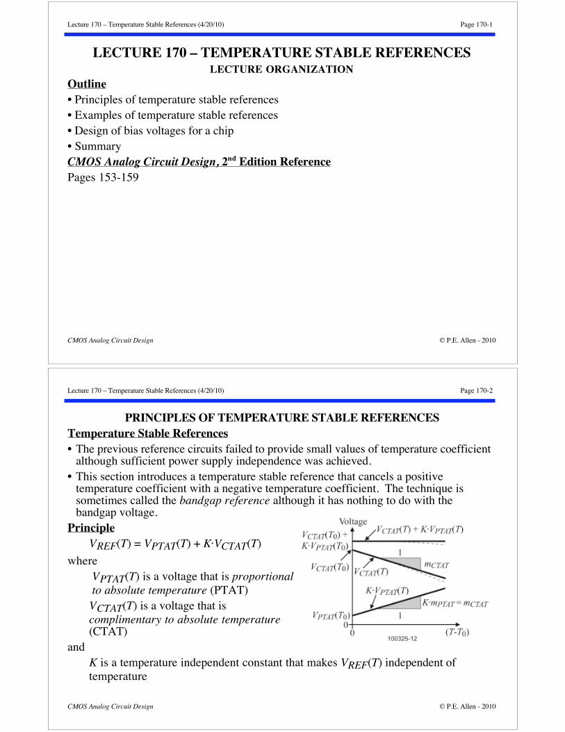
Lecture 170 – Temperature Stable References (4/20/10) Page 170-1 CMOS Analog Circuit Design © P.E. Allen - 2010 LECTURE 170 – TEMPERATURE STABLE REFERENCES LECTURE ORGANIZATION Outline • Principles of temperature stable references • Examples of temperature stable references • Design of bias voltages for a chip • Summary CMOS Analog Circuit Design, 2 nd Edition Reference Pages 153-159 Lecture 170 – Temperature Stable References (4/20/10) Page 170-2 CMOS Analog Circuit Design © P.E. Allen - 2010 PRINCIPLES OF TEMPERATURE STABLE REFERENCES Temperature Stable References • The previous reference circuits failed to provide small values of temperature coefficient although sufficient power supply independence was achieved. • This section introduces a temperature stable reference that cancels a positive temperature coefficient with a negative temperature coefficient. The technique is sometimes called the bandgap reference although it has nothing to do with the bandgap voltage. Principle V REF (T) = V PTAT (T) + K·V CTAT (T) where V PTAT (T) is a voltage that is proportional to absolute temperature (PTAT) V CTAT (T) is a voltage that is complimentary to absolute temperature (CTAT) and K is a temperature independent constant that makes V REF (T) independent of temperature
Transcript of LECTURE 170 – TEMPERATURE STABLE...
Lecture 170 – Temperature Stable References (4/20/10) Page 170-1
CMOS Analog Circuit Design © P.E. Allen - 2010
LECTURE 170 – TEMPERATURE STABLE REFERENCESLECTURE ORGANIZATION
Outline• Principles of temperature stable references• Examples of temperature stable references• Design of bias voltages for a chip• SummaryCMOS Analog Circuit Design, 2nd Edition ReferencePages 153-159
Lecture 170 – Temperature Stable References (4/20/10) Page 170-2
CMOS Analog Circuit Design © P.E. Allen - 2010
PRINCIPLES OF TEMPERATURE STABLE REFERENCESTemperature Stable References• The previous reference circuits failed to provide small values of temperature coefficient
although sufficient power supply independence was achieved.• This section introduces a temperature stable reference that cancels a positive
temperature coefficient with a negative temperature coefficient. The technique issometimes called the bandgap reference although it has nothing to do with thebandgap voltage.
PrincipleVREF(T) = VPTAT(T) + K·VCTAT(T)
whereVPTAT(T) is a voltage that is proportionalto absolute temperature (PTAT)VCTAT(T) is a voltage that iscomplimentary to absolute temperature(CTAT)
andK is a temperature independent constant that makes VREF(T) independent oftemperature
Lecture 170 – Temperature Stable References (4/20/10) Page 170-3
CMOS Analog Circuit Design © P.E. Allen - 2010
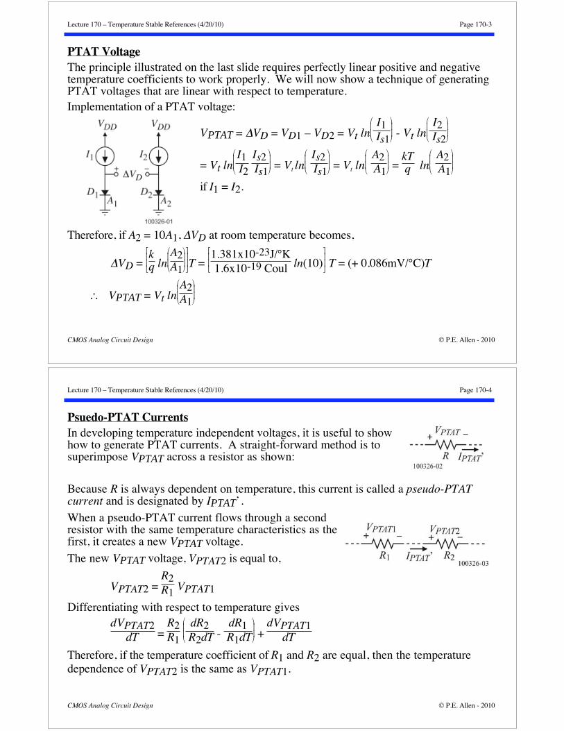
PTAT VoltageThe principle illustrated on the last slide requires perfectly linear positive and negativetemperature coefficients to work properly. We will now show a technique of generatingPTAT voltages that are linear with respect to temperature.Implementation of a PTAT voltage:
VPTAT = VD = VD1 – VD2 = Vt lnI1Is1 - Vt ln
I2Is2
= Vt lnI1I2
Is2Is1 = Vt ln
Is2Is1 = Vt ln
A2A1 =
kTq ln
A2A1
if I1 = I2.
Therefore, if A2 = 10A1, VD at room temperature becomes,
VD = kq ln
A2A1 T =
1.381x10⁻²³J/°K1.6x10-19 Coul ln(10) T = (+ 0.086mV/°C)T
VPTAT = Vt lnA2A1
Lecture 170 – Temperature Stable References (4/20/10) Page 170-4
CMOS Analog Circuit Design © P.E. Allen - 2010
Psuedo-PTAT CurrentsIn developing temperature independent voltages, it is useful to showhow to generate PTAT currents. A straight-forward method is tosuperimpose VPTAT across a resistor as shown:
Because R is always dependent on temperature, this current is called a pseudo-PTATcurrent and is designated by IPTAT’.
When a pseudo-PTAT current flows through a secondresistor with the same temperature characteristics as thefirst, it creates a new VPTAT voltage.
The new VPTAT voltage, VPTAT2 is equal to,
VPTAT2 = R2R1 VPTAT1
Differentiating with respect to temperature givesdVPTAT2
dT = R2R1
dR2R2dT -
dR1R1dT +
dVPTAT1dT
Therefore, if the temperature coefficient of R1 and R2 are equal, then the temperaturedependence of VPTAT2 is the same as VPTAT1.
Lecture 170 – Temperature Stable References (4/20/10) Page 170-5
CMOS Analog Circuit Design © P.E. Allen - 2010
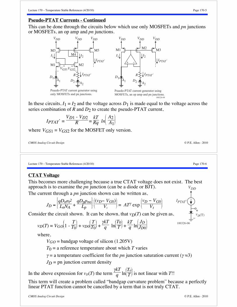
Pseudo-PTAT Currents - ContinuedThis can be done through the circuits below which use only MOSFETs and pn junctionsor MOSFETs, an op amp and pn junctions.
In these circuits, I1 = I2 and the voltage across D1 is made equal to the voltage across theseries combination of R and D2 to create the pseudo-PTAT current,
IPTAT’ = VD1 - VD2
R = kTRq ln
A2A1
where VGS1 = VGS2 for the MOSFET only version.
Psuedo-PTAT current generator using
only MOSFETs and pn junctions.
VDD
I1
VDD
I2
+
−VGS1
D1D2A1 A2
Μ1 Μ2
Μ3Μ4
+
−VGS2
R IPTAT’
VDD
Μ5
IPTAT’
Psuedo-PTAT current generator using
MOSFETs, an op amp and pn junctions.
VDD
I1
VDD
I2
D1D2A1 A2
Μ1 Μ2 Μ3
R IPTAT’
VDD
IPTAT’+ −
100326-04
Lecture 170 – Temperature Stable References (4/20/10) Page 170-6
CMOS Analog Circuit Design © P.E. Allen - 2010
CTAT VoltageThis becomes more challenging because a true CTAT voltage does not exist. The bestapproach is to examine the pn junction (can be a diode or BJT).The current through a pn junction shown can be written as,
JD = qDnni2
LnNA+
qDppno
Lp
(vD VG0)Vt
= AT exp vD VG0
Vt
Consider the circuit shown. It can be shown, that vD(T) can be given as,
vD(T) = VGO 1 -TT0 + vD0
TT0 +
kTq ln
T0T +
kTq ln
JDJD0
where,VGO = bandgap voltage of silicon (1.205V)T0 = a reference temperature about which T varies
= a temperature coefficient for the pn junction saturation current ( 3)JD = pn junction current density
In the above expression for vD(T) the term kTq ln
T0
T is not linear with T!!
This term will create a problem called “bandgap curvature problem” because a perfectlylinear PTAT function cannot be cancelled by a term that is not truly CTAT.

Lecture 170 – Temperature Stable References (4/20/10) Page 170-7
CMOS Analog Circuit Design © P.E. Allen - 2010
Pseudo CTAT CurrentsThe circuits below show two ways of creating a pseudo CTAT current using negativefeedback:†
The negative feedback loop shown causes the current designated as ICTAT’ to be,
ICTAT’ = VBE
R = VDR
† I.M. Gunawan, G.C.M. Jeijer, J. Fonderie, and J.H. Huijsing, “A Curvature-Corrected Low-Voltage Bandgap Reference, IEEE J. Solid-state Circuits, vol. SC-28, No. 6, June1993, pp. 677-670.
Lecture 170 – Temperature Stable References (4/20/10) Page 170-8
CMOS Analog Circuit Design © P.E. Allen - 2010
Temperature Independent Voltage ReferencesBasic structures:
Series form:
VREF = IPTAT’R2 + VD = R2R1
VPTAT + VCTAT
Parallel form:
VREF = (IPTAT’ + ICTAT’)R3 + VD = R3R1
VPTAT + R3R2
VCTAT = R3R2
R2R1
VPTAT + VCTAT
To achieve temperature independence, VREF must be differentiated with respect totemperature and set equal to zero. The resistor ratios and other parameters can be usedto achieve temperature independence.

Lecture 170 – Temperature Stable References (4/20/10) Page 170-9
CMOS Analog Circuit Design © P.E. Allen - 2010
Conditions for Temperature IndependenceDifferentiating either the series or parallel form with respect to temperature and equatingto zero gives,
K = R2R1
= - dVCTAT/dTdVPTAT/dT
The slopes of VCTAT and VPTAT at a given temperature, T0, are:
mCTAT = dVCTAT
dT
|T=T0
= VD - VGO
T0 + ( - )
k
q =
VCTAT - VGO
T0 + ( - )
Vt0
T0
where = temperature dependence of JD [JD(T) T , where = 1 for PTATcurrent flowing through the pn junction]
and
mPTAT = dVPTAT
dT
|T=T0
= k
q ln
JD2
JD1 =
k
q ln
A2
A1 =
Vt0
T0 ln
A2
A1 =
VPTAT
T0
Therefore, the temperature independent constant multiplying VPTAT is
Temp. independent constant = K = R2R1 =
VGO - VCTAT + ( - )Vt0VPTAT
Therefore,VREF = VGO-VCTAT + ( - )Vt0 + VCTAT = VGO + ( - )Vt0 1.205V+0.057 = 1.262V
Lecture 170 – Temperature Stable References (4/20/10) Page 170-10
CMOS Analog Circuit Design © P.E. Allen - 2010
Example 170-1 – Temp. Independent Constant for Series and Parallel References(a.) Design the ratio of R2/R1 for the series configuration if VCTAT = 0.6V and A2/A1 = 10for room temperature (Vt = 0.026V). Assume = 3.2 and = 1. Find the value of VREF.
R2R1 =
VGO - VCTAT + ( - )Vt0VPTAT =
1.205 - 0.6 + 2.2(0.026)0.026(2.3026) = 11.06
VREF = 1.205 + 2.2(0.026) = 1.262V(b.) For the parallel configuration find the values of R2/R1 and R3/R2 if VREF = 0.5V.
From (a.) we know that R2/R1 = 11.05. We also know that,
VREF = R3R1
VPTAT + R3R2
VCTAT = R3R2
R2R1
VPTAT + VCTAT
= (R3/R2)[11.05ln(10)(0.026) + 0.6] = (R3/R2)1.262 = 0.5
(R3/R2) = 0.3963
If R1 = 1k , then R2 = 11.05k and R3 = 4.378k

Lecture 170 – Temperature Stable References (4/20/10) Page 170-11
CMOS Analog Circuit Design © P.E. Allen - 2010
A Series Temperature Independent Voltage ReferenceAn early realization of the series form is shown below†:Assuming VOS = 0, then VR1 is
VR1 = VEB2 - VEB1 = Vt lnJ2Js2
- Vt lnJ1Js1
= Vt lnI2AE1I1AE2
= Vt lnR2AE1R1AE2
The op amp forces the relationship I1R2 = I2R3
VREF = VEB2+I2R3 = VEB2+VR1R2R1
= VEB2+ R2R1
VtlnR2AE1R1AE2
= VCTAT+ R2R1
lnR2AE1R1AE2
Vt
Differentiating the above with respect to temperature and setting the result to zero, givesR2R1
lnR2AE1R1AE2
= VGO - VCTAT + ( - )Vt0
Vt
If VOS 0, then VREF becomes,
VREF = VEB2 - 1 +R2R1
VOS + R2R1
Vt lnR2AE1R1AE2
1 -VOSI1R2
† K.E. Kujik, “A Precision Reference Voltage Source,” IEEE Journal of Solid-State Circuits, Vol. SC-8, No. 3 (June 1973) pp. 222-226.
Lecture 170 – Temperature Stable References (4/20/10) Page 170-12
CMOS Analog Circuit Design © P.E. Allen - 2010
Example 170-2 – Design of the Previous Temperature Independent ReferenceAssume that AE1 = 10 AE2, VEB2 = 0.7 V, R2 = R3, and Vt = 0.026 V at room temperaturefor temperature independent reference on the previous slide. Find R2/R1 to give a zerotemperature coefficient at room temperature. If VOS = 10 mV, find the change in VREF. Notethat I1R2 = VREF VEB2 VOS.
Evaluating the temperature independent constant gives
R2R1
ln R2 AE1R3AE2
= VGO - VCTAT + ( - )Vt0
VPTAT =
1.205 - 0.7 + (2.2)(0.026)0.026 = 21.62
Therefore, R2/R1 = 9.39. In order to use the equation for VREF with VOS 0, we mustknow the approximate value of VREF and iterate if necessary because I1 is a function ofVREF. Assuming VREF to be 1.262, we obtain from
VREF = VEB2 - 1 +R2R1
VOS + R2R1
Vt lnR2AE1R1AE2
1 -VOS
VREF - VEB2 - VOS
a new value VREF = 1.153 V. The second iteration makes little difference on the resultbecause VREF is in the argument of the logarithm

Lecture 170 – Temperature Stable References (4/20/10) Page 170-13
CMOS Analog Circuit Design © P.E. Allen - 2010
Series Temperature Independent Voltage ReferencesThe references shown do not use an op amp and avoid the issues with offset voltage andPSRR.
I1 = IPTAT’ = VBE2 - VBE1
R2 =
Vt
R2 ln
I2
Is2 - ln
I1
Is1
= VtR2
lnIs1Is2
= VtR2
lnAE1AE2
Since I1= I2, VREF = VBE2 + I1R1 = VBE1 + R1R2
lnAE1AE2
Vt
= VCTAT + R1R2
lnAE1AE2
VPTAT
VD1 = I2R1 + VD2
I3 = I2 = IPTAT’ = VtR ln(n)
VREF = VD3 + I3(kR) = VD3 + kVt ln(n) = VCTAT + k ln(n)VPTAT
Lecture 170 – Temperature Stable References (4/20/10) Page 170-14
CMOS Analog Circuit Design © P.E. Allen - 2010
Parallel Temperature Independent Voltage ReferenceA parallel form of the temperature independent voltage reference is shown below:
VREF = R3R1
VPTAT + R3R2
VCTAT
Comments:• The BJT of the ICTAT’ generator can be replaced with an MOSFET-diode equivalent• Any value of VREF can be achieved• Part (b.) of Example 170-1 showed how to design the resistors of this implementation

Lecture 170 – Temperature Stable References (4/20/10) Page 170-15
CMOS Analog Circuit Design © P.E. Allen - 2010
How Can a Bandgap “Current” Reference be Obtained?Use a MOSFET under ZTC operation and design the parallel form of the bandgap voltagereference to give a value of VZTC.
060529-09
VDD
IPTAT
VDD
IVBE
R3+
−VREF =VGS(ZTC)
IREF
Lecture 170 – Temperature Stable References (4/20/10) Page 170-16
CMOS Analog Circuit Design © P.E. Allen - 2010
Bandgap Curvature Problem
Unfortunately, the kTq ln
T0
T term of the pnjunction contributed a nonlinearity to theCTAT realization. This is illustrated by thedashed lines in the plot shown.The result is shown below where the referencevoltage is not constant with temperature.
Comments:• True temperature independence is only achieved over a small range of temperatures• References that do not correct this problem have a temperature dependence of 10
ppm°/C to 50 ppm/°C over 0°C to 70°C.

Lecture 170 – Temperature Stable References (4/20/10) Page 170-17
CMOS Analog Circuit Design © P.E. Allen - 2010
Some Curvature Correction Techniques• Squared PTAT Correction:
Temperature coefficient 1-20 ppm/°C
• VBE loop
M. Gunaway, et. al., “A Curvature-Corrected Low-Voltage BandgapReference,” IEEE Journal of Solid-State Circuits, vol. 28, no. 6, pp. 667-670, June 1993.
• ß compensationI. Lee et. al., “Exponential Curvature-Compensated BiCMOS BandgapReferences,” IEEE Journal of Solid-State Circuits, vol. 29, no. 11, pp. 1396-1403,Nov. 1994.
• Nonlinear cancellationG.M. Meijer et. al., “A New Curvature-Corrected Bandgap Reference,” IEEEJournal of Solid-State Circuits, vol. 17, no. 6, pp. 1139-1143, December 1982.
VBE VPTAT
VRef = VBE + VPTAT + VPTAT2
Temperature
Vol
tage
Fig. 400-01
VPTAT2
Lecture 170 – Temperature Stable References (4/20/10) Page 170-18
CMOS Analog Circuit Design © P.E. Allen - 2010
VBE Loop Curvature Correction Technique
Circuit:Operation:
INL = VBE1-VBE2
R3 =
VtR3
lnIc1A2A1Ic2
= VtR3
ln2IPTAT
INL+IConstantwhere
Iconstant = INL + IPTAT + IVBE
INL + VtRx
+ VBER2
(a quasi-temperature independent current subject to the TCF of the resistors)where
Vt = kT/qIc1 and Ic2 are the collector currents of Qn1 and Qn2, respectivelyRx = a resistor used to define IPTAT
VREF = VBER2
+VtR3
ln2IPTAT
INL + Iconstant+ IPTAT R1
VDD VDD VDDIPTAT IPTAT
IPTAT
INL
IVBE+INL
IVBE
IConstantQn1x1
Qn2x2R2
R3 VREF
3-Output Current Mirror (IVBE+INL)
VDD
Fig. 400-02
R1
Temperature coefficient 3 ppm/°C with a total quiescent current of 95μA.

Lecture 170 – Temperature Stable References (4/20/10) Page 170-19
CMOS Analog Circuit Design © P.E. Allen - 2010
ß Compensation Curvature Correction TechniqueCircuit: Operation:
VREF = VBE + AT +BT
(1+ß) R VBE + AT +BTß R
whereA and B are constantT = temperature
The temperature dependence of ß is
ß(T) e-1/T ß(T) = Ce-1/T
VREF = VBE(T) + AT +BTe1/T
C
Not good for small values of Vin.
Vin VREF + Vsat. = VGO + Vsat. = 1.4V
I=AT I=BT
RVREF
Vin
BT1+ß
Fig. 400-0
Lecture 170 – Temperature Stable References (4/20/10) Page 170-20
CMOS Analog Circuit Design © P.E. Allen - 2010
Series Temperature Independent Voltage Reference with Curvature CorrectionObjective: Eliminate nonlinear term from VCTAT.
Result: 0.5 ppm/°C from -25°C to 85°C.Operation: VREF = VPTAT + 3VCTAT – 2VConstant
Note that, IPTAT Ic T 1 = 1and IConstant Ic T 0 = 0,Previously we found,
VCTAT(T) VGO - TT0
VGO-VCTAT(T0) -( - )Vt lnTT0
so that
VCTAT(IPTAT) =VGO-TT0
VGO-VBE(T0) -( -1)Vt lnTT0
and
VCTAT(IConstant) =VGO - TT0
VGO -VCTAT(T0) - Vt lnTT0
Combining the above relationships gives, VREF(T) = VPTAT + VGO - (T/T0)[VGO - VCTAT(T0)] - [ - 3] Vt ln (T/T0)
If 3, then VREF(T) VPTAT + VGO 1 - (T/T0) + VCTAT(T0)(T/T0)

Lecture 170 – Temperature Stable References (4/20/10) Page 170-21
CMOS Analog Circuit Design © P.E. Allen - 2010
A Parallel Version of the Nonlinear Curvature Correction TechniqueThe last idea was good in concept but not appropriate for CMOS implementation. Thefollowing is a better implementation.
VREF = R0[IPTAT’ + ICTAT’ – Iconst.] = R0R1
VPTAT + R0R2
VCTAT - R0R3
Vconst.
Use the resistor ratios to eliminate the nonlinear term given and .
Lecture 170 – Temperature Stable References (4/20/10) Page 170-22
CMOS Analog Circuit Design © P.E. Allen - 2010
Parallel Curvature Correction Reference - ContinuedSubstitute for VCTAT and Vconst. in the expression for VREF.
VREF = R0R1
VPTAT + R0R2
VGO-TT0
VGO-VCTAT(T0) -( -1)Vt lnTT0
- R0R3
VGO-TT0
VGO-VCTAT(T0) - Vt lnTT0
To cancel the nonlinear CTAT term, we want the following relationship to hold:R0R2
( -1) = R0R3
R2R3
= ( -1)
(Fortunately is always greater than 1)
With these constraints, we find the voltage reference to be,
VREF = R0R1
VPTAT + R0R2
-R0R3
VGO-TT0
VGO-VCTAT(T0)
= R0R1
VPTAT + 1 R0R2
VGO-TT0
VGO-VCTAT(T0)
= R0R2
R2R1
VPTAT+ VGO-TT0
VGO-VCTAT(T0) = R0R2
R2R1
VPTAT+VCTAT(T0) , (T = T0)
Design R2/R1 to achieve temperature independence and R0/R2 to get VREF.

Lecture 170 – Temperature Stable References (4/20/10) Page 170-23
CMOS Analog Circuit Design © P.E. Allen - 2010
Example 170-3 – Design of a Zero Temperature Coefficient Voltage ReferenceAssume that VCTAT = 0.7 V, R3 = 10k , = 3.2, A2 = 10A1, and Vt = 0.026 V at room
temperature for the parallel curvature correction circuit. Find R2 and R3 to give a zerotemperature coefficient at room temperature and a reference voltage of 1.0V.
To eliminate the nonlinear CTAT term,R2R3
= ( -1)
= (2.2)3.2 = 0.6875 R2 = 6.88k
To cancel the temperature dependence,
Temp. independent constant = K = R2
R1=
VGO - VCTAT + ( - )Vt0VPTAT
orR2R1
= VGO - VCTAT + ( - )Vt0
VPTAT = (1.205 0.7 + (3.2-1)(0.026)
(0.026)(2.3026) = 9.3907 R1=2.34k
The reference voltage can be written as,
VREF = R0R2
R2R1
VPTAT+VCTAT(T0) = R0R2
[9.3907(0.026)(2.3026) + 0.7]
R0R2
= (3.2)1.262 = 2.535 R0 = 2.535R2 = 17.44k
Lecture 170 – Temperature Stable References (4/20/10) Page 170-24
CMOS Analog Circuit Design © P.E. Allen - 2010
Other Characteristics of Bandgap Voltage ReferencesNoise
Voltage references for high-resolution ADCs are particularly sensitive to noise.Noise sources: Op amp, resistors, switches, etc.
PSRRMaximize the PSRR of the op amp.
Offset VoltagesBecomes a problem when op amps are used.VBE2 = VBE1 + VR1 + VOS
VBE = VBE2 - VBE1 = VR1 + VOS = Vt lniC2AE1
iC1AE2
Since iC2R3 = iC1R2 - VOS
then iC2
iC1 =
R2
R3 -
VOS
iC1R3 =
R2
R3 1 +
VOS
iC1R2
Therefore,
VR1 = -VOS + Vt lnR2AE1
R3AE21 +
VOS
iC1R2
VREF = VBE2 - VOS + iC1R2 = VBE2 - VOS + VR1
R1R2 = VBE2 - VOS +
R2
R1
VREF = VBE2 - VOS 1+R2
R1+
R2
R1Vt ln
R2AE1
R3AE21 -
VOS
iC1R2
Fig. 400-05
iC1iC2
VCC
Q1Q2
+-
+
VREF
-
VEE
VOS
R3 R2
R1
+
-VR1

Lecture 170 – Temperature Stable References (4/20/10) Page 170-25
CMOS Analog Circuit Design © P.E. Allen - 2010
Noise Analysis of a Bandgap ReferenceConsider the simple classical BG reference shown(R2 = 10 R1 = 10k ):
The open-circuit output noise voltage squared isfound as,
eno2 = [en12/R12 + en22/R12 + gm52en32
+ gm52en42 + gm52en52 + ind12/(gm12R12)
+ ind22 + ind32 + inr12 + inr22] R22
Assuming the MOSFETs are matched and the dccurrents in D1, D2, and D3 are equal gives,
eno2 [gm52(en32+en42+en52) + ind22+ ind32 + inr12 + inr22] R22
Thermal noise gives (gm5 = 400μS),
eno2 = 8kTgm52R22+4qI1+
4kTR1 +
4kTR2 R22 5.3x10⁻¹⁹+6.4x10⁻²³+1.7x10⁻¹⁵(V2/Hz)
1/f noise gives,
060605-02
VDD
M1 M2
M3M4
x1
+
−
eno2
i2i1
D1D2 D3
xn xn
M5
i3
** *en32 en42 en52
* *en12 en22
ind12
inr12R1 R2
ind22
inr22
ind32
eno2 = 3gm52 KF
2fCoxWL K’
Lecture 170 – Temperature Stable References (4/20/10) Page 170-26
CMOS Analog Circuit Design © P.E. Allen - 2010
DESIGN OF BIAS VOLTAGES FOR A CHIPDistributing Bias Voltages over a DistanceThe major problem is the IR drops in busses. For example,
100µA
100µA
1mm
M1 M2VBias
050716-01
ID1 ID2100µA
If the bus metal is 50m /sq. and is 5μm wide, the resistance of the bus in one direction is(50m /sq.)x(1000μm/5μm) = 10 . The difference in drain currents for an overdrive of0.1V is,
VGS1 = 1mV + VGS2 + 1mV = VGS2 + 2mV
ID1ID2 =
(VGS1-VTN)2
(VGS2-VTN)2 = (VGS2-VTN+2mV)2
(VGS2-VTN)2 = 0.1+0.002
0.12= 1.04

Lecture 170 – Temperature Stable References (4/20/10) Page 170-27
CMOS Analog Circuit Design © P.E. Allen - 2010
Use Current to Avoid IR Drops in Long Metal LinesExample:
Lecture 170 – Temperature Stable References (4/20/10) Page 170-28
CMOS Analog Circuit Design © P.E. Allen - 2010
Practical Aspects of Temperature-Independent and Supply-Independent BiasingA temperature-independent and supply-independent current source and its distribution:
The currents are used to distribute the bias voltages to remote sections of the chip.

Lecture 170 – Temperature Stable References (4/20/10) Page 170-29
CMOS Analog Circuit Design © P.E. Allen - 2010
Practical Aspects of Bias Distribution Circuits - Continued
Distribution of the current avoids change in bias voltage due to IR drop in bias lines.
Slave bias circuit:
From here on out in these notes, VPBias1 = VPB1 = VDD-|VTP|-VSD(sat) VPBias2 = VPB2 = VDD-|VTP|-2VSD(sat)
andVNBias1 = VNB1 = VTN + VDS(sat) VNBias2 = VNB2 = VTN + 2VDS(sat)
From Master Bias
Ib Ib
VDD
VPBias1
VPBias2
VNBias2
VNBias1
Fig. 400-08
Lecture 170 – Temperature Stable References (4/20/10) Page 170-30
CMOS Analog Circuit Design © P.E. Allen - 2010
SUMMARY OF TEMPERATURE STABLE REFERENCES• The classical form of the temperature stable reference has a value of voltage close to the
bandgap voltage and is called the “bandgap voltage reference”.• Bandgap voltage references can achieve temperature dependence less than 50 ppm/°C• Correction of second-order effects in the bandgap voltage reference can achieve very
stable (1 ppm/°C) voltage references.• Watch out for second-order effects such as noise when using the bandgap voltage
reference in sensitive applications.• Distribution of bias voltages over a long distance should be done by current rather than
voltage.


![100420 Final TGP Summary Report[1]](https://static.fdocuments.in/doc/165x107/577d37321a28ab3a6b950f95/100420-final-tgp-summary-report1.jpg)