Lecture 10: MultiUser MEMS Process (MUMPS) - Mechanical Engineering
34
1 Lecture 10: MultiUser MEMS Process (MUMPS) Prasanna S. Gandhi Assistant Professor, Department of Mechanical Engineering, Indian Institute of Technology, Bombay, MEMS: Fabrication
Transcript of Lecture 10: MultiUser MEMS Process (MUMPS) - Mechanical Engineering
PolyMUMPS Surface Micromachining Process
1
1
Lecture 10: MultiUser MEMS Process
(MUMPS)
Prasanna S. GandhiAssistant Professor,Department of Mechanical Engineering,Indian Institute of Technology, Bombay,
MEMS: Fabrication
PolyMUMPS Surface Micromachining Process
2
2
Recap
Various VLSI based fabrication processes and detailsSome design fundamentalsSensors and actuators for MEMS
PolyMUMPS Surface Micromachining Process
3
3
Today
Pressure sensor: full fabrication animationMUMPSDetails of PolyMUMPs processDesign rulesLedit software to develop your device by polyMUMPs processExamples of the devices made by polyMUMPS
PolyMUMPS Surface Micromachining Process
4
4
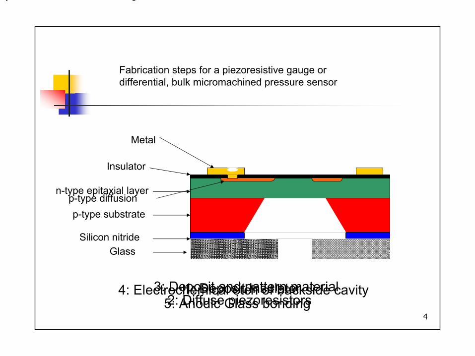
Insulator
n-type epitaxial layer
p-type substrate
Silicon nitride
1: Deposit Insulator
p-type diffusion
2: Diffuse piezoresistors
Metal
3: Deposit and pattern material4: Electrochemical etch of backside cavity
Glass
5: Anodic Glass bonding
Fabrication steps for a piezoresistive gauge or differential, bulk micromachined pressure sensor
PolyMUMPS Surface Micromachining Process
5
5
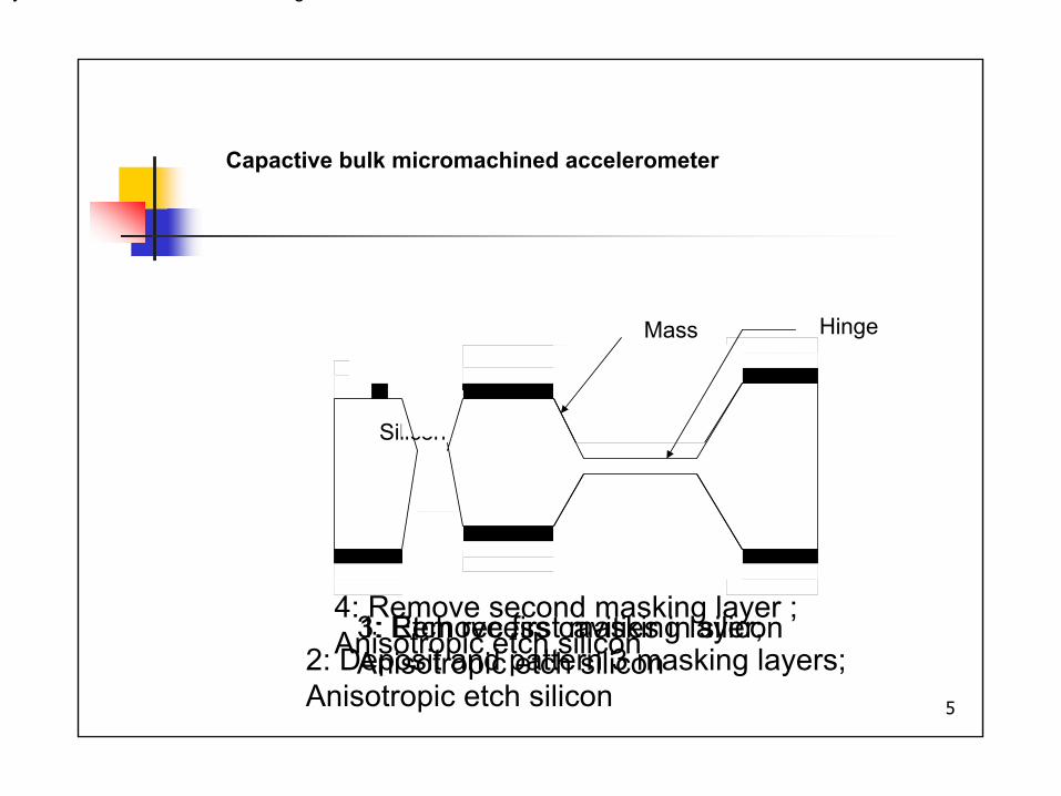
Silicon
1: Etch recess cavities in silicon2: Deposit and pattern 3 masking layers;Anisotropic etch silicon
3: Remove first masking layer;Anisotropic etch silicon
Mass Hinge
4: Remove second masking layer ;Anisotropic etch silicon
Capactive bulk micromachined accelerometer
PolyMUMPS Surface Micromachining Process
6
6
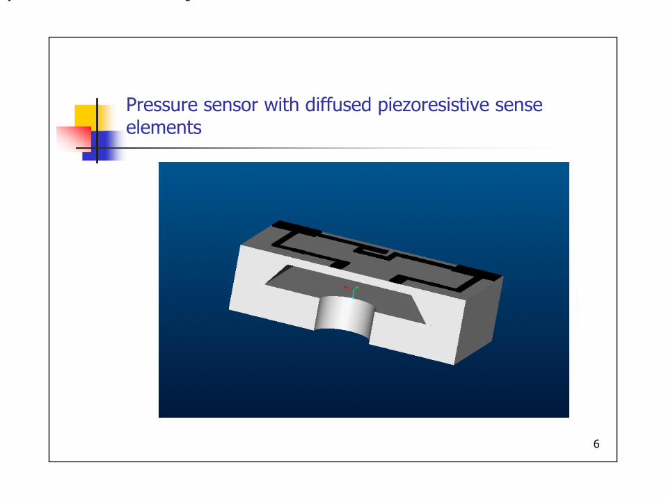
Pressure sensor with diffused piezoresistive sense elements
PolyMUMPS Surface Micromachining Process
7
7
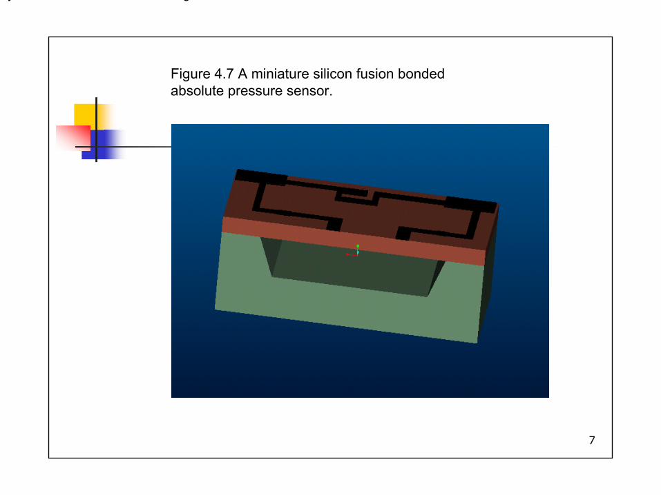
Figure 4.7 A miniature silicon fusion bonded absolute pressure sensor.
PolyMUMPS Surface Micromachining Process
8
8
MUMPs Process
Multi User MEMS processCompany MEMSCAP: offers PolyMUMPS, MetalMUMPS, and SOIMUMPSDeveloped at BSAC (Berkeley Sensors and Actuators Center) in late 80’s
We will study PolyMUMPs a 3 level polysiliconmicromachining process
PolyMUMPS Surface Micromachining Process
9
9
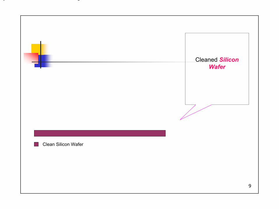
Cleaned Silicon Wafer
Clean Silicon Wafer
PolyMUMPS Surface Micromachining Process
10
10
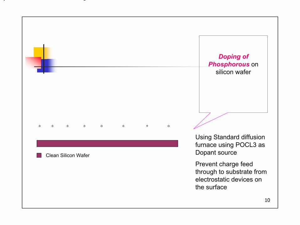
Doping of Phosphorous on
silicon wafer
Using Standard diffusion furnace using POCL3 as Dopant source
Prevent charge feed through to substrate from electrostatic devices on the surface
Clean Silicon Wafer
PolyMUMPS Surface Micromachining Process
11
11
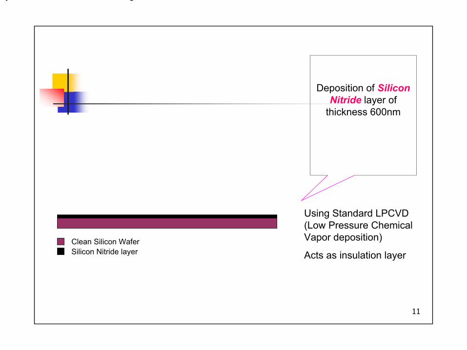
Deposition of Silicon Nitride layer of
thickness 600nm
Using Standard LPCVD (Low Pressure Chemical Vapor deposition)
Acts as insulation layerClean Silicon WaferSilicon Nitride layer
PolyMUMPS Surface Micromachining Process
12
12
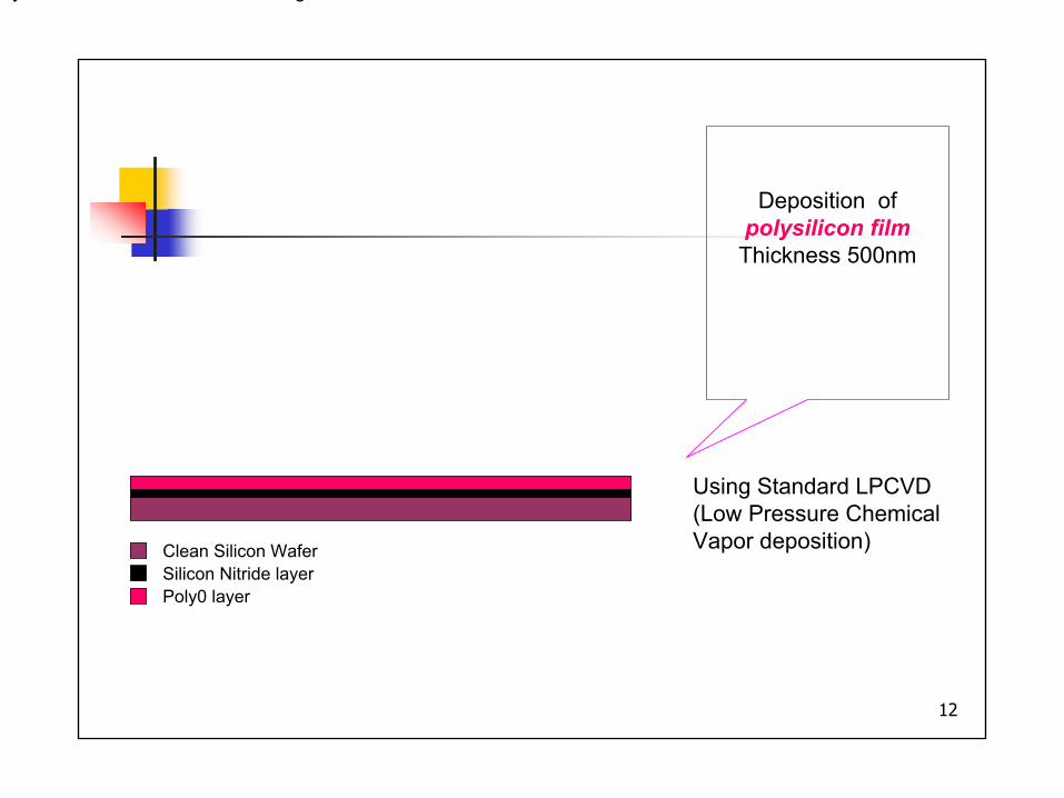
Deposition of polysilicon filmThickness 500nm
Using Standard LPCVD (Low Pressure Chemical Vapor deposition) Clean Silicon Wafer
Silicon Nitride layerPoly0 layer
PolyMUMPS Surface Micromachining Process
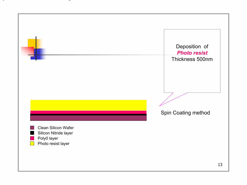
13
13
Deposition of Photo resist
Thickness 500nm
Spin Coating method
Clean Silicon WaferSilicon Nitride layerPoly0 layerPhoto resist layer
PolyMUMPS Surface Micromachining Process
14
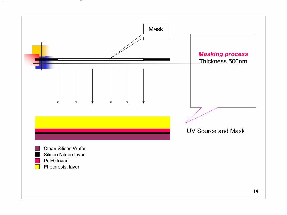
14
Masking processThickness 500nm
Mask
Clean Silicon WaferSilicon Nitride layerPoly0 layerPhotoresist layer
UV Source and Mask
PolyMUMPS Surface Micromachining Process
15
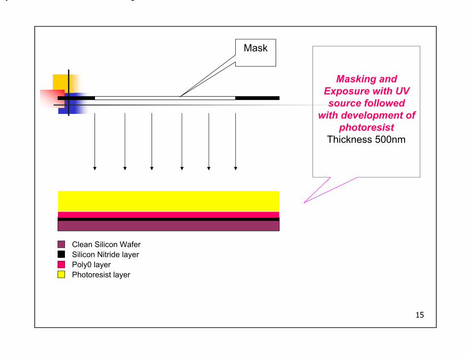
15
Masking and Exposure with UV source followed
with development of photoresist
Thickness 500nm
Mask
Clean Silicon WaferSilicon Nitride layerPoly0 layerPhotoresist layer
PolyMUMPS Surface Micromachining Process
16
16
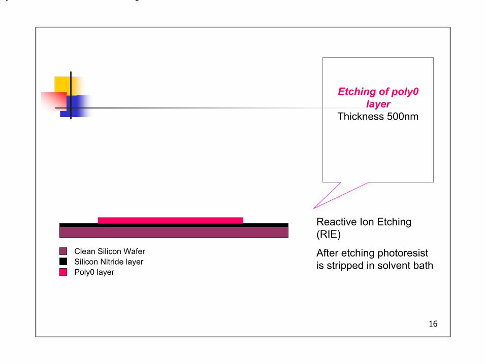
Etching of poly0 layer
Thickness 500nm
Clean Silicon WaferSilicon Nitride layerPoly0 layer
Reactive Ion Etching (RIE)
After etching photoresist is stripped in solvent bath
PolyMUMPS Surface Micromachining Process
17
17
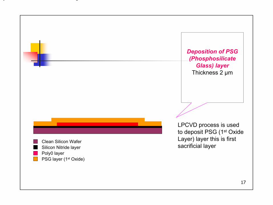
Deposition of PSG (Phosphosilicate
Glass) layer Thickness 2 µm
Clean Silicon WaferSilicon Nitride layerPoly0 layerPSG layer (1st Oxide)
LPCVD process is used to deposit PSG (1st Oxide Layer) layer this is first sacrificial layer
PolyMUMPS Surface Micromachining Process
18
18
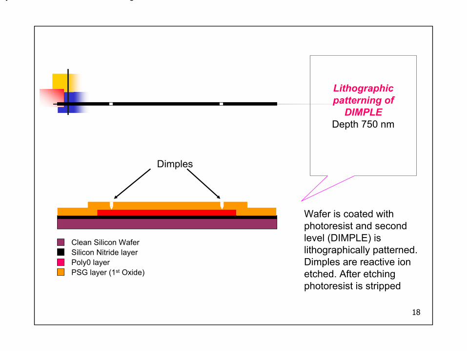
Lithographic patterning of
DIMPLEDepth 750 nm
Clean Silicon WaferSilicon Nitride layerPoly0 layerPSG layer (1st Oxide)
Dimples
Wafer is coated with photoresist and second level (DIMPLE) is lithographically patterned. Dimples are reactive ion etched. After etching photoresist is stripped
PolyMUMPS Surface Micromachining Process
19
19
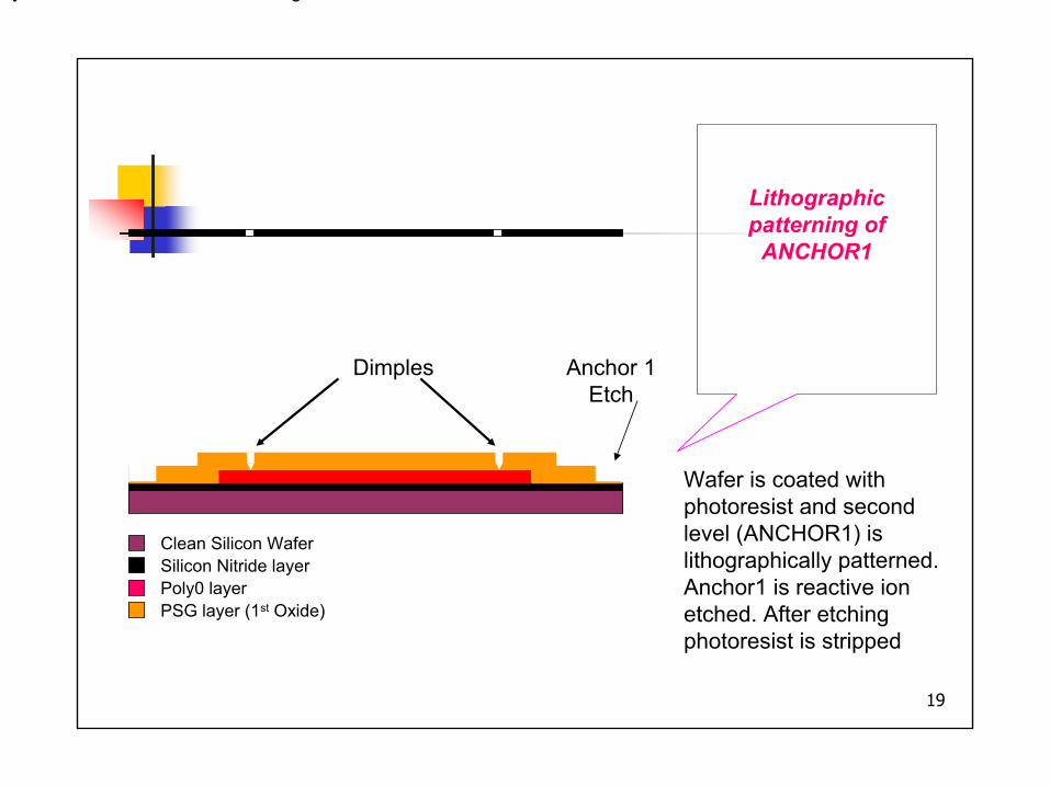
Lithographic patterning of
ANCHOR1
Clean Silicon WaferSilicon Nitride layerPoly0 layerPSG layer (1st Oxide)
Dimples Anchor 1 Etch
Wafer is coated with photoresist and second level (ANCHOR1) is lithographically patterned. Anchor1 is reactive ion etched. After etching photoresist is stripped
PolyMUMPS Surface Micromachining Process
20
20
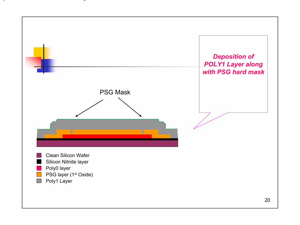
Deposition of POLY1 Layer along with PSG hard mask
Clean Silicon WaferSilicon Nitride layerPoly0 layerPSG layer (1st Oxide)
PSG Mask
Poly1 Layer
PolyMUMPS Surface Micromachining Process
21
21
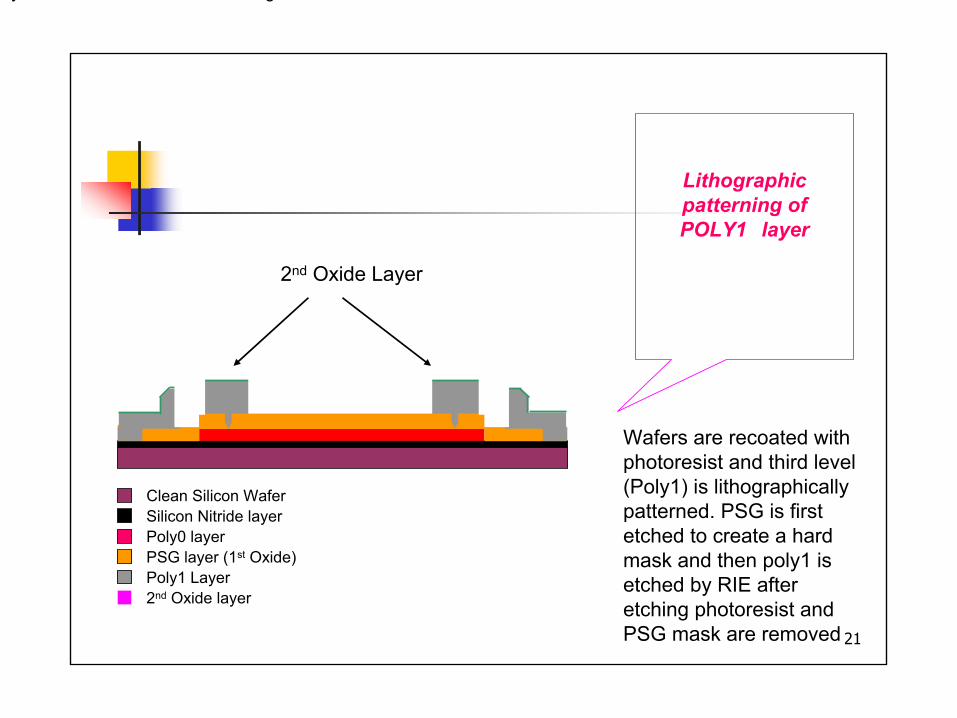
Lithographic patterning of POLY1 layer
Clean Silicon WaferSilicon Nitride layerPoly0 layerPSG layer (1st Oxide)Poly1 Layer
2nd Oxide Layer
2nd Oxide layer
Wafers are recoated with photoresist and third level (Poly1) is lithographically patterned. PSG is first etched to create a hard mask and then poly1 is etched by RIE after etching photoresist and PSG mask are removed
PolyMUMPS Surface Micromachining Process
22
22
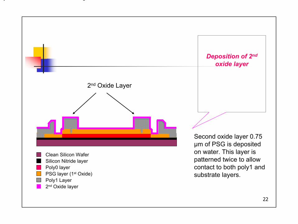
Deposition of 2nd
oxide layer
Clean Silicon WaferSilicon Nitride layerPoly0 layerPSG layer (1st Oxide)Poly1 Layer
2nd Oxide Layer
2nd Oxide layer
Second oxide layer 0.75 µm of PSG is deposited on water. This layer is patterned twice to allow contact to both poly1 and substrate layers.
PolyMUMPS Surface Micromachining Process
23
23
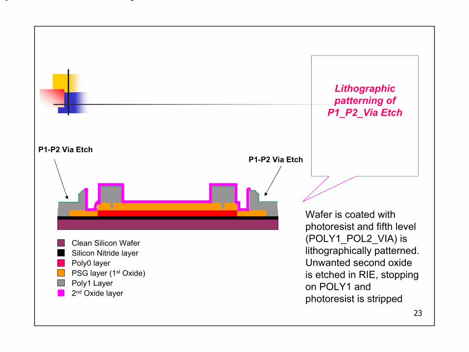
Lithographic patterning of
P1_P2_Via Etch
Clean Silicon WaferSilicon Nitride layerPoly0 layerPSG layer (1st Oxide)Poly1 Layer2nd Oxide layer
P1-P2 Via EtchP1-P2 Via Etch
Wafer is coated with photoresist and fifth level (POLY1_POL2_VIA) is lithographically patterned. Unwanted second oxide is etched in RIE, stopping on POLY1 and photoresist is stripped
PolyMUMPS Surface Micromachining Process
24
24
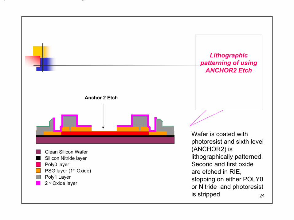
Lithographic patterning of using
ANCHOR2 Etch
Clean Silicon WaferSilicon Nitride layerPoly0 layerPSG layer (1st Oxide)Poly1 Layer2nd Oxide layer
Anchor 2 Etch
Wafer is coated with photoresist and sixth level (ANCHOR2) is lithographically patterned. Second and first oxide are etched in RIE, stopping on either POLY0 or Nitride and photoresist is stripped
PolyMUMPS Surface Micromachining Process
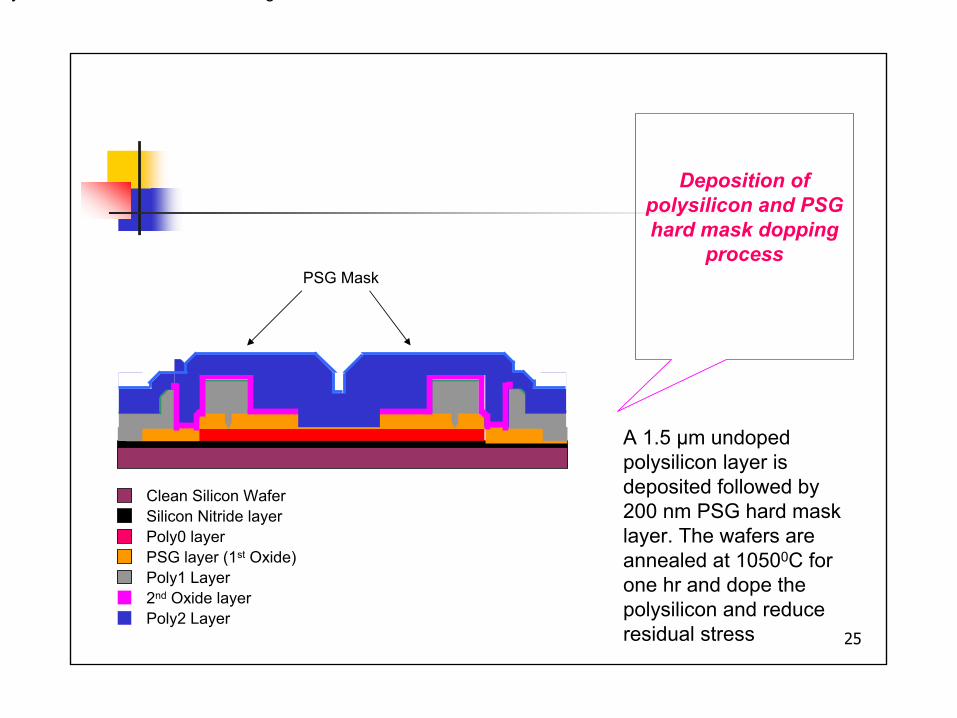
25
25
Deposition of polysilicon and PSG hard mask dopping
process
Clean Silicon WaferSilicon Nitride layerPoly0 layerPSG layer (1st Oxide)Poly1 Layer2nd Oxide layer
PSG Mask
Poly2 Layer
A 1.5 µm undoped polysilicon layer is deposited followed by 200 nm PSG hard mask layer. The wafers are annealed at 10500C for one hr and dope the polysilicon and reduce residual stress
PolyMUMPS Surface Micromachining Process
26
26
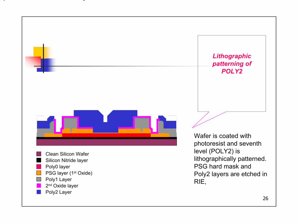
Lithographic patterning of
POLY2
Clean Silicon WaferSilicon Nitride layerPoly0 layerPSG layer (1st Oxide)Poly1 Layer2nd Oxide layerPoly2 Layer
Wafer is coated with photoresist and seventh level (POLY2) is lithographically patterned. PSG hard mask and Poly2 layers are etched in RIE,
PolyMUMPS Surface Micromachining Process
27
27
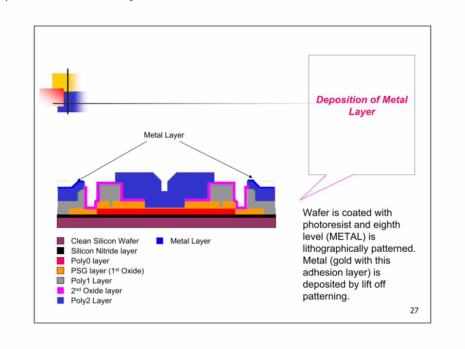
Deposition of Metal Layer
Clean Silicon WaferSilicon Nitride layerPoly0 layerPSG layer (1st Oxide)Poly1 Layer2nd Oxide layer
Metal Layer
Poly2 Layer
Metal Layer
Wafer is coated with photoresist and eighth level (METAL) is lithographically patterned. Metal (gold with this adhesion layer) is deposited by lift off patterning.
PolyMUMPS Surface Micromachining Process
28
28
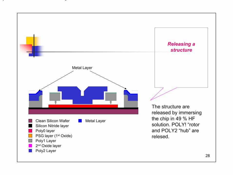
Releasing a structure
Clean Silicon WaferSilicon Nitride layerPoly0 layerPSG layer (1st Oxide)Poly1 Layer2nd Oxide layer
Metal Layer
Poly2 Layer
Metal Layer
The structure are released by immersing the chip in 49 % HF solution. POLY! “rotor and POLY2 “hub” are relesed.
PolyMUMPS Surface Micromachining Process
29
29
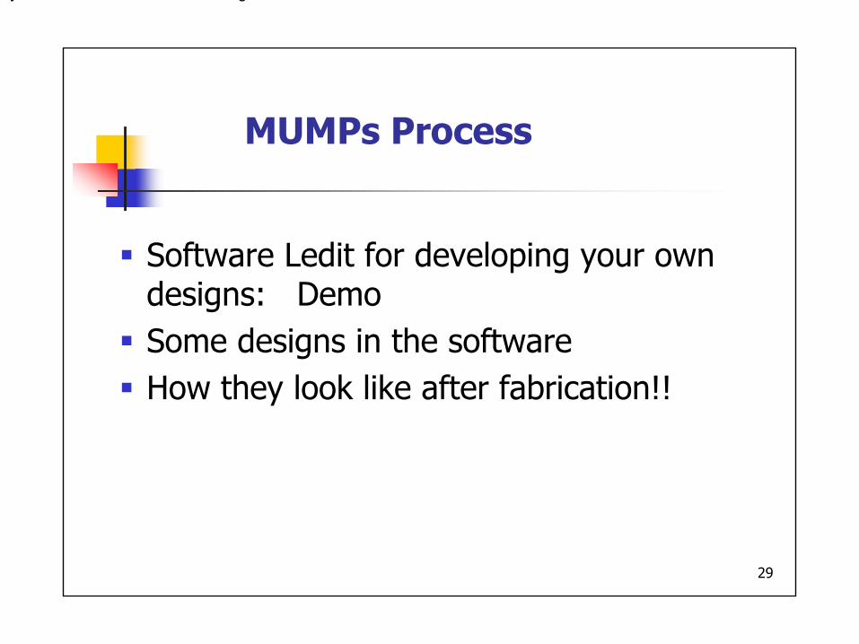
MUMPs Process
Software Ledit for developing your own designs: DemoSome designs in the softwareHow they look like after fabrication!!
PolyMUMPS Surface Micromachining Process
30
30
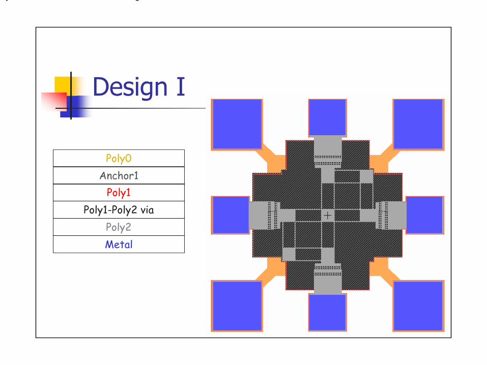
Design I
Poly0
Poly1Poly1-Poly2 via
Poly2Metal
Anchor1
PolyMUMPS Surface Micromachining Process
31
31
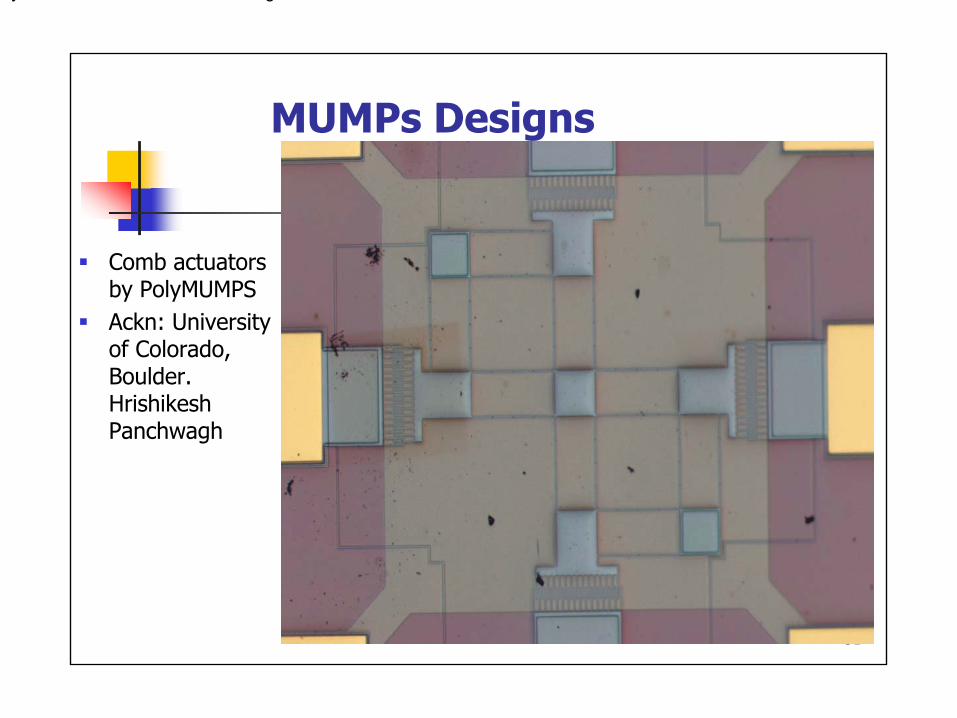
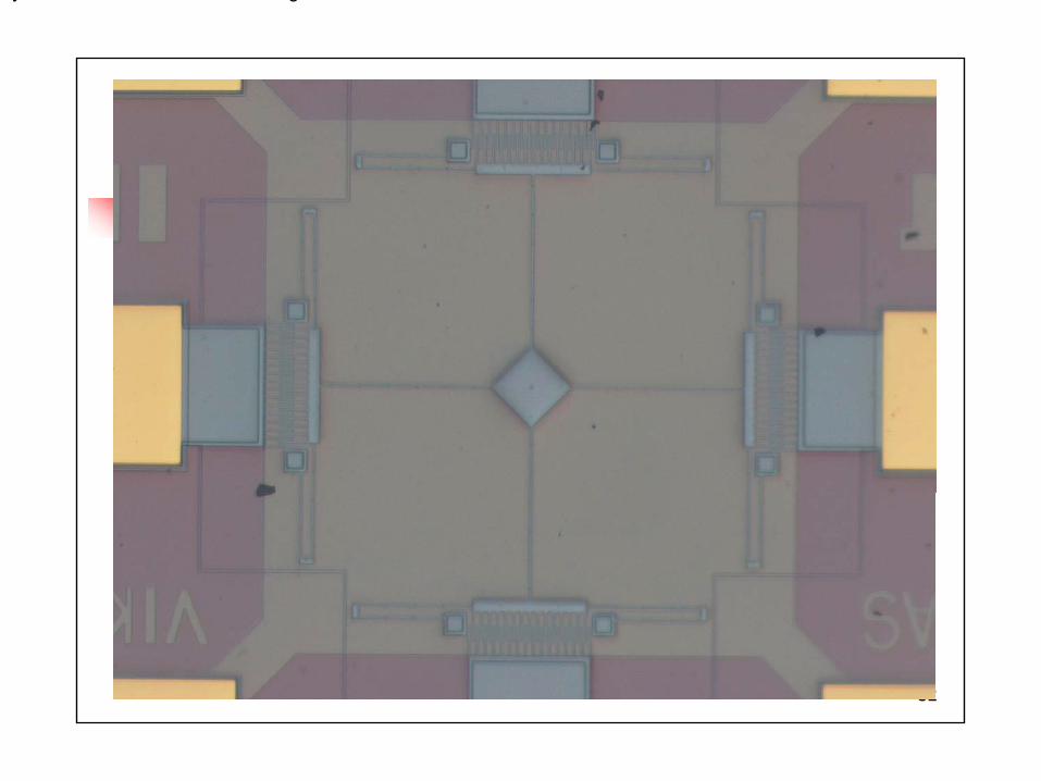
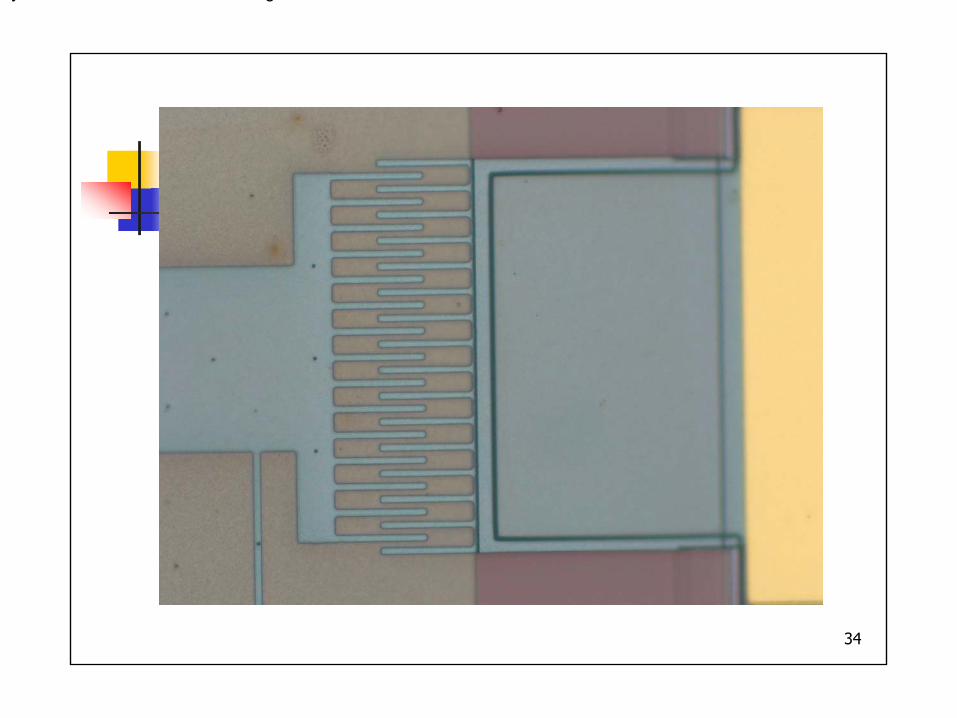
MUMPs Designs and Products
Comb actuators by PolyMUMPSAckn: University of Colorado, Boulder. HrishikeshPanchwagh
PolyMUMPS Surface Micromachining Process
32
32
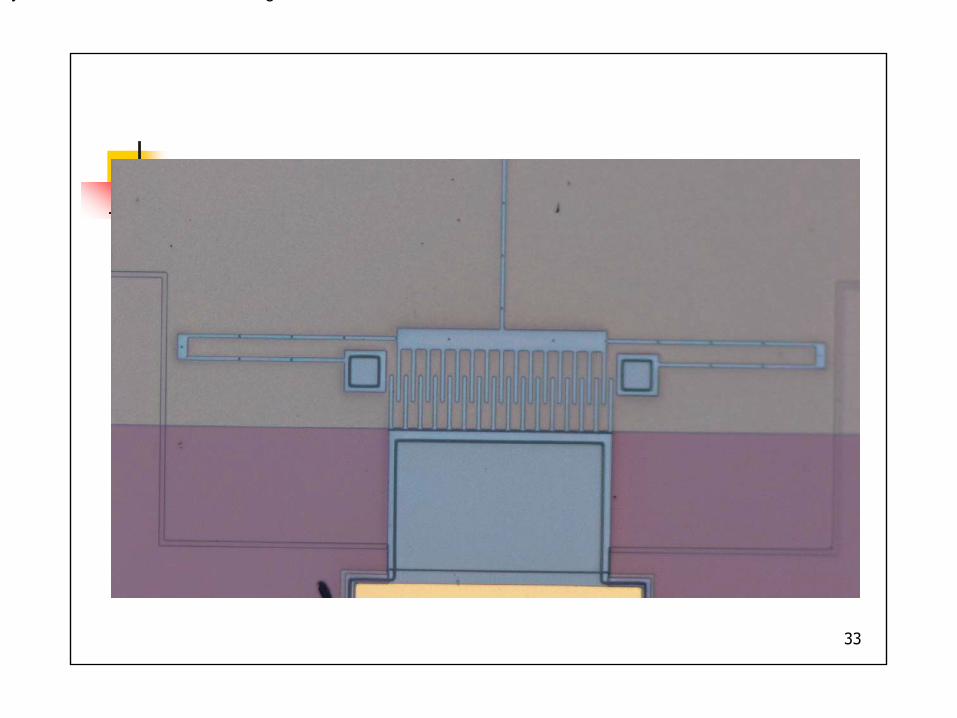
PolyMUMPS Surface Micromachining Process
33
33
PolyMUMPS Surface Micromachining Process
34
34