
LECTURE 10 MOS CAPACITOR MODEL AND LARGE SIGNAL … · Lecture 10 – MOS Capacitor Model and Large...
32
Lecture 10 – MOS Capacitor Model and Large Signal Model Dependence (3/10/14) Page 10-1 CMOS Analog Circuit Design © P.E. Allen - 2016 LECTURE 10 – MOS CAPACITOR MODEL AND LARGE SIGNAL MODEL DEPENDENCE LECTURE ORGANIZATION Outline • MOSFET capacitor model • Dependence of the large signal model on process • Dependence of the large signal model on voltage • Dependence of the large signal model on temperature • MOSFET reliability • Summary CMOS Analog Circuit Design, 3 rd Edition Reference Pages 77-86 and new material
Transcript of LECTURE 10 MOS CAPACITOR MODEL AND LARGE SIGNAL … · Lecture 10 – MOS Capacitor Model and Large...
Lecture 10 – MOS Capacitor Model and Large Signal Model Dependence (3/10/14) Page 10-1
CMOS Analog Circuit Design © P.E. Allen - 2016
LECTURE 10 – MOS CAPACITOR MODEL AND LARGE
SIGNAL MODEL DEPENDENCE
LECTURE ORGANIZATION
Outline
• MOSFET capacitor model
• Dependence of the large signal model on process
• Dependence of the large signal model on voltage
• Dependence of the large signal model on temperature
• MOSFET reliability
• Summary
CMOS Analog Circuit Design, 3rd Edition Reference
Pages 77-86 and new material
Lecture 10 – MOS Capacitor Model and Large Signal Model Dependence (3/10/14) Page 10-2
CMOS Analog Circuit Design © P.E. Allen - 2016
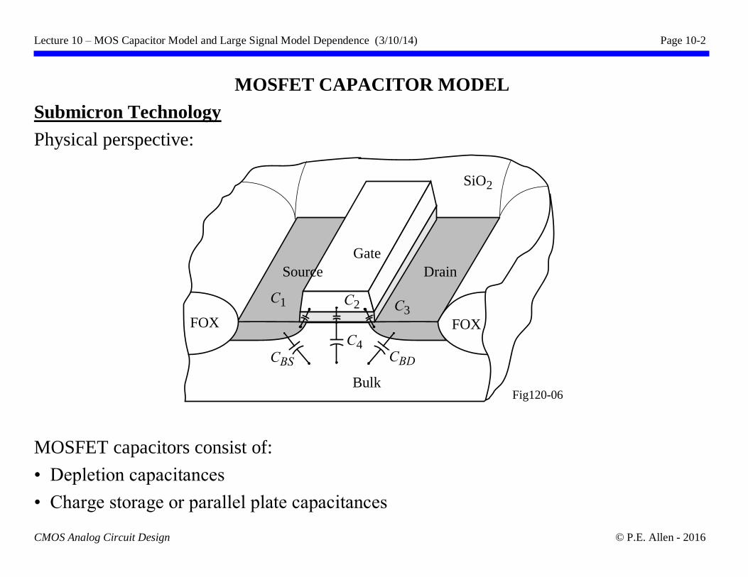
MOSFET CAPACITOR MODEL
Submicron Technology
Physical perspective:
MOSFET capacitors consist of:
• Depletion capacitances
• Charge storage or parallel plate capacitances
SiO2
Bulk
Source Drain
Gate
CBS CBD
C4
C1 C2 C3
Fig120-06
FOX FOX
Lecture 10 – MOS Capacitor Model and Large Signal Model Dependence (3/10/14) Page 10-3
CMOS Analog Circuit Design © P.E. Allen - 2016
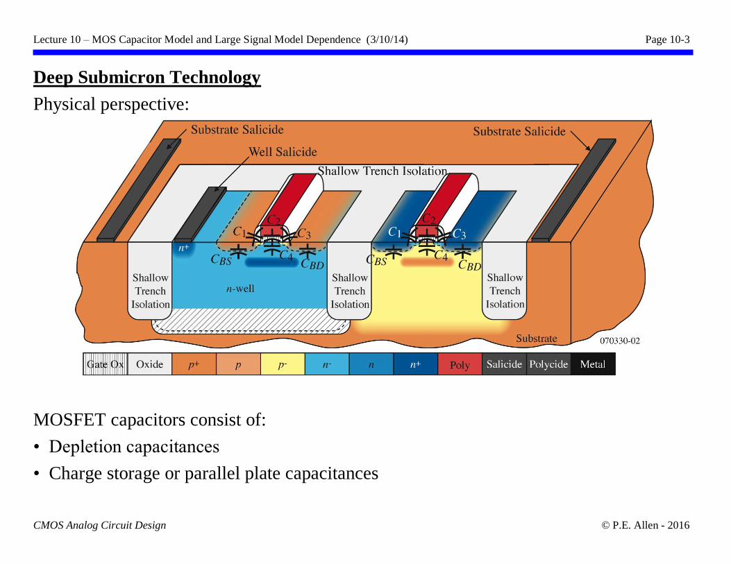
Deep Submicron Technology
Physical perspective:
MOSFET capacitors consist of:
• Depletion capacitances
• Charge storage or parallel plate capacitances
Lecture 10 – MOS Capacitor Model and Large Signal Model Dependence (3/10/14) Page 10-4
CMOS Analog Circuit Design © P.E. Allen - 2016
MOSFET Depletion Capacitors
Model:
1.) vBS FC·PB
CBS = CJ·AS
1 - vBS
PB
MJ
+ CJSW·PS
1 - vBS
PB
MJSW
,
and
2.) vBS> FC·PB
CBS = CJ·AS
1- FC1+MJ
1 - (1+MJ)FC + MJ VBS
PB
+ CJSW·PS
1 - FC1+MJSW
1 - (1+MJSW)FC + MJSW VBS
PB
SiO2
Polysilicon gate
Bulk
A B
CD
EF
GH
Drain bottom = ABCD
Drain sidewall = ABFE + BCGF + DCGH + ADHE
Source Drain
Fig. 120-07
where
AS = area of the source
PS = perimeter of the source
CJSW = zero bias, bulk source sidewall capacitance
MJSW = bulk-source sidewall grading coefficient
For the bulk-drain depletion capacitance replace "S" by "D" in the above.
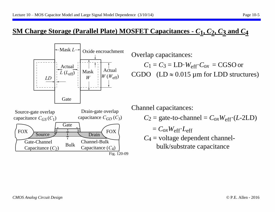
Lecture 10 – MOS Capacitor Model and Large Signal Model Dependence (3/10/14) Page 10-5
CMOS Analog Circuit Design © P.E. Allen - 2016
SM Charge Storage (Parallel Plate) MOSFET Capacitances - C1, C2, C3 and C4
Overlap capacitances:
C1 = C3 = LD·Weff·Cox = CGSO or
CGDO (LD 0.015 µm for LDD structures)
Channel capacitances:
C2 = gate-to-channel = CoxWeff·(L-2LD)
= CoxWeff·Leff
C4 = voltage dependent channel-
bulk/substrate capacitance
Bulk
LD
Mask
W
Oxide encroachment
Actual
L (Leff)
Gate
Mask L
Source-gate overlap
capacitance CGS (C1)
Drain-gate overlap
capacitance CGD (C3)
Actual
W (Weff)
Fig. 120-09
Source
Gate
Drain
Gate-Channel
Capacitance (C2)
Channel-Bulk
Capacitance (C4)
FOX FOX
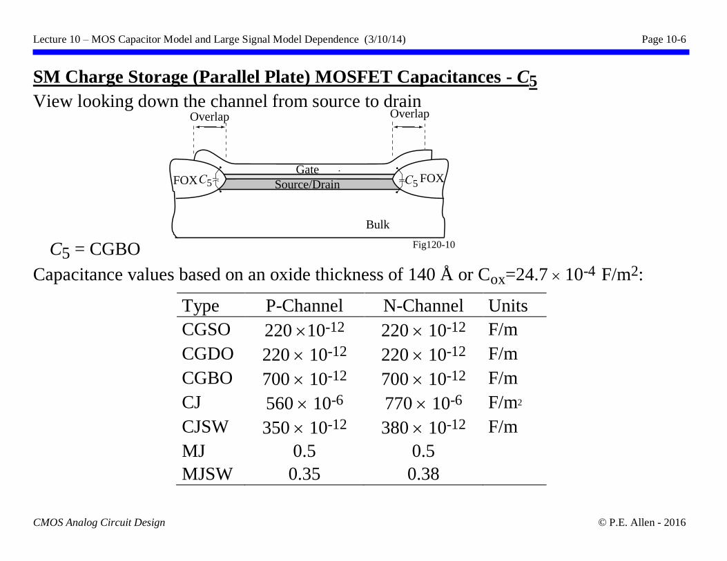
Lecture 10 – MOS Capacitor Model and Large Signal Model Dependence (3/10/14) Page 10-6
CMOS Analog Circuit Design © P.E. Allen - 2016
SM Charge Storage (Parallel Plate) MOSFET Capacitances - C5
View looking down the channel from source to drain
C5 = CGBO
Capacitance values based on an oxide thickness of 140 Å or Cox=24.7 10-4 F/m2:
Type P-Channel N-Channel Units
CGSO 220 10-12 220 10-12 F/m
CGDO 220 10-12 220 10-12 F/m
CGBO 700 10-12 700 10-12 F/m
CJ 560 10-6 770 10-6 F/m2
CJSW 350 10-12 380 10-12 F/m
MJ 0.5 0.5
MJSW 0.35 0.38
Bulk
Overlap Overlap
Source/Drain
GateFOX FOXC5 C5
Fig120-10
Lecture 10 – MOS Capacitor Model and Large Signal Model Dependence (3/10/14) Page 10-7
CMOS Analog Circuit Design © P.E. Allen - 2016
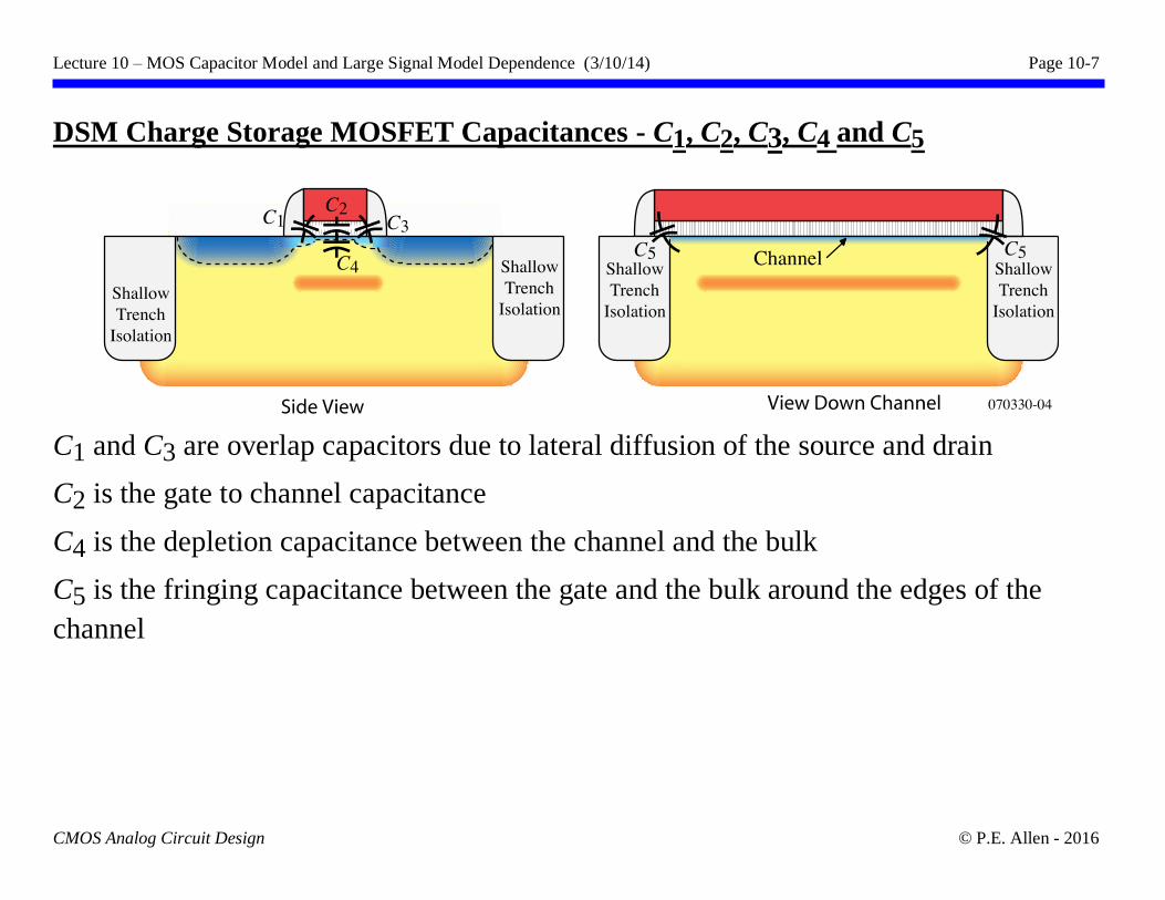
DSM Charge Storage MOSFET Capacitances - C1, C2, C3, C4 and C5
C1 and C3 are overlap capacitors due to lateral diffusion of the source and drain
C2 is the gate to channel capacitance
C4 is the depletion capacitance between the channel and the bulk
C5 is the fringing capacitance between the gate and the bulk around the edges of the
channel
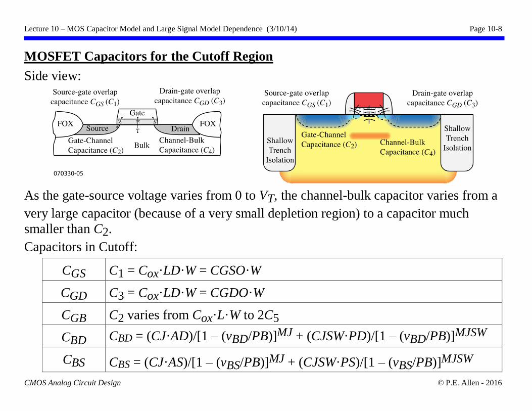
Lecture 10 – MOS Capacitor Model and Large Signal Model Dependence (3/10/14) Page 10-8
CMOS Analog Circuit Design © P.E. Allen - 2016
MOSFET Capacitors for the Cutoff Region
Side view:
As the gate-source voltage varies from 0 to VT, the channel-bulk capacitor varies from a
very large capacitor (because of a very small depletion region) to a capacitor much
smaller than C2.
Capacitors in Cutoff:
CGS C1 = Cox·LD·W = CGSO·W
CGD C3 = Cox·LD·W = CGDO·W
CGB C2 varies from Cox·L·W to 2C5
CBD CBD = (CJ·AD)/[1 – (vBD/PB)]MJ + (CJSW·PD)/[1 – (vBD/PB)]MJSW
CBS CBS = (CJ·AS)/[1 – (vBS/PB)]MJ + (CJSW·PS)/[1 – (vBS/PB)]MJSW
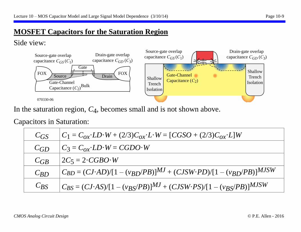
Lecture 10 – MOS Capacitor Model and Large Signal Model Dependence (3/10/14) Page 10-9
CMOS Analog Circuit Design © P.E. Allen - 2016
MOSFET Capacitors for the Saturation Region
Side view:
In the saturation region, C4, becomes small and is not shown above.
Capacitors in Saturation:
CGS C1 = Cox·LD·W + (2/3)Cox·L·W = [CGSO + (2/3)Cox·L]W
CGD C3 = Cox·LD·W = CGDO·W
CGB 2C5 = 2·CGBO·W
CBD CBD = (CJ·AD)/[1 – (vBD/PB)]MJ + (CJSW·PD)/[1 – (vBD/PB)]MJSW
CBS CBS = (CJ·AS)/[1 – (vBS/PB)]MJ + (CJSW·PS)/[1 – (vBS/PB)]MJSW
Bulk
Source-gate overlap
capacitance CGS (C1)
Drain-gate overlap
capacitance CGD (C3)
Source
Gate
Drain
Gate-Channel
Capacitance (C2)
FOX FOXShallow
Trench
Isolation
Shallow
Trench
Isolation
070330-06
Source-gate overlap
capacitance CGS (C1)
Drain-gate overlap
capacitance CGD (C3)
Gate-Channel
Capacitance (C2)
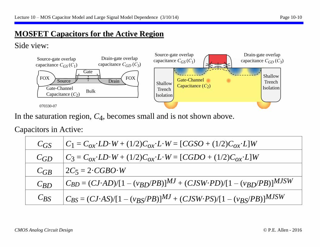
Lecture 10 – MOS Capacitor Model and Large Signal Model Dependence (3/10/14) Page 10-10
CMOS Analog Circuit Design © P.E. Allen - 2016
MOSFET Capacitors for the Active Region
Side view:
In the saturation region, C4, becomes small and is not shown above.
Capacitors in Active:
CGS C1 = Cox·LD·W + (1/2)Cox·L·W = [CGSO + (1/2)Cox·L]W
CGD C3 = Cox·LD·W + (1/2)Cox·L·W = [CGDO + (1/2)Cox·L]W
CGB 2C5 = 2·CGBO·W
CBD CBD = (CJ·AD)/[1 – (vBD/PB)]MJ + (CJSW·PD)/[1 – (vBD/PB)]MJSW
CBS CBS = (CJ·AS)/[1 – (vBS/PB)]MJ + (CJSW·PS)/[1 – (vBS/PB)]MJSW
Bulk
Source-gate overlap
capacitance CGS (C1)
Drain-gate overlap
capacitance CGD (C3)
Source
Gate
Drain
Gate-Channel
Capacitance (C2)
FOX FOXShallow
Trench
Isolation
Shallow
Trench
Isolation
070330-07
Source-gate overlap
capacitance CGS (C1)
Drain-gate overlap
capacitance CGD (C3)
Gate-Channel
Capacitance (C2)
Lecture 10 – MOS Capacitor Model and Large Signal Model Dependence (3/10/14) Page 10-11
CMOS Analog Circuit Design © P.E. Allen - 2016
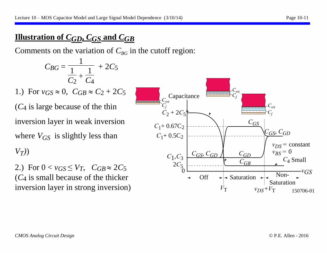
Illustration of CGD, CGS and CGB
Comments on the variation of CBG in the cutoff region:
CBG = 1
1
C2 +
1
C4
+ 2C5
1.) For vGS 0, CGB C2 + 2C5
(C4 is large because of the thin
inversion layer in weak inversion
where VGS is slightly less than
VT))
2.) For 0 < vGS ≤ VT, CGB 2C5 (C4 is small because of the thicker
inversion layer in strong inversion)
0 vGS
CGS
CGS, CGD
CGD
CGB
CGS, CGD
C2 + 2C5
C1+ 0.67C2
C1, C3
2C5
VT vDS +VT
Off Saturation Non-
Saturation
vDS = constant vBS = 0
Capacitance
C1+ 0.5C2
150706-01
C4 Small
CoxCj
CoxCj
Cox
Cj
Lecture 10 – MOS Capacitor Model and Large Signal Model Dependence (3/10/14) Page 10-12
CMOS Analog Circuit Design © P.E. Allen - 2016
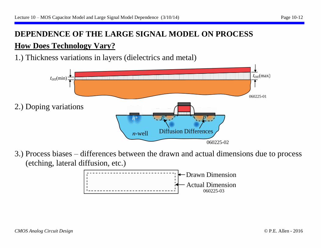
DEPENDENCE OF THE LARGE SIGNAL MODEL ON PROCESS
How Does Technology Vary?
1.) Thickness variations in layers (dielectrics and metal)
2.) Doping variations
3.) Process biases – differences between the drawn and actual dimensions due to process
(etching, lateral diffusion, etc.)
060225-01
tox(min)tox(max)
060225-03
Drawn Dimension
Actual Dimension
060225-02
n-well
p+n+ p+
Diffusion Differences
Lecture 10 – MOS Capacitor Model and Large Signal Model Dependence (3/10/14) Page 10-13
CMOS Analog Circuit Design © P.E. Allen - 2016
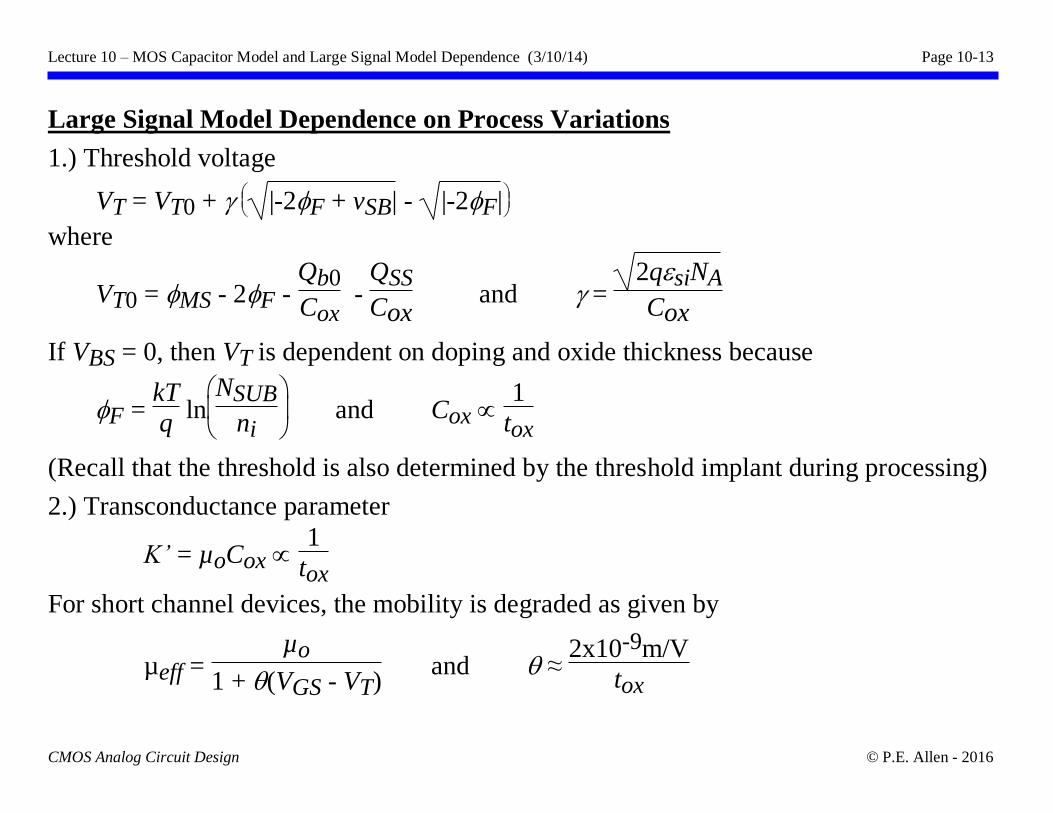
Large Signal Model Dependence on Process Variations
1.) Threshold voltage
VT = VT0 +
|-2F + vSB| - |-2F|
where
VT0 = MS - 2F - Qb0
Cox -
QSS
Cox and =
2qsiNA
Cox
If VBS = 0, then VT is dependent on doping and oxide thickness because
F = kT
q ln
NSUB
ni and Cox
1
tox
(Recall that the threshold is also determined by the threshold implant during processing)
2.) Transconductance parameter
K’ = µoCox 1
tox
For short channel devices, the mobility is degraded as given by
µeff = µo
1 + (VGS - VT) and ≈
2x10⁻⁹m/V
tox
Lecture 10 – MOS Capacitor Model and Large Signal Model Dependence (3/10/14) Page 10-14
CMOS Analog Circuit Design © P.E. Allen - 2016
Process Variation “Corners”
For strong inversion operation, the primary influence is the oxide thickness, tox. We see
that K’ will tend to increase with decreasing oxide thickness whereas VT tends to
decrease.
If the “speed” of a transistor is increased
by increasing K’ and decreasing VT, then
the variation of technology can be
expressed on a two-dimensional graph
resulting in a rectangular area of
“acceptable” process limitation.
Three corner versus five corner models
060118-10
PMOS
Speed
NMOS Speed
Fast
PMOS
Slow
PMOS
Slow
NMOS
Fast
NMOS
Acceptable
Technology
Parameters
Large Kʼ
Small VT
Small Kʼ
Large VT
Lecture 10 – MOS Capacitor Model and Large Signal Model Dependence (3/10/14) Page 10-15
CMOS Analog Circuit Design © P.E. Allen - 2016
DEPENDENCE OF THE LARGE SIGNAL MODEL ON VOLTAGE
What is Voltage Variation?
Voltage variation is the influence of power supply voltage on the component.
(There is also power supply influence on the circuit called power supply rejection ratio,
PSRR. We will deal with this in a later lecture.)
Power supply variation comes from:
1.) Influence of depletion region widths on components.
2.) Nonlinearity (e.g., velocity saturation)
3.) Breakdown voltage
Note: Because the large-signal model for the MOSFET includes all the influences of
voltage on the transistor, we will focus on passive components except for breakdown.
Lecture 10 – MOS Capacitor Model and Large Signal Model Dependence (3/10/14) Page 10-16
CMOS Analog Circuit Design © P.E. Allen - 2016
Models for Voltage Dependence of a Component
1.) ith-order Voltage Coefficients
In general a variable y = f(v) which is a function of voltage, v, can be expressed as a
Taylor series,
y(v = V0) y(V0) + a1(v- V0) + a2(v- V0)2+ a3(v- V0)3 + ···
where the coefficients, ai, are defined as,
a1 = df(v)
dv|
v=V0 , a2 =
1
2 d2f(v)
dv2
|v=V0
, ….
The coefficients, ai, are called the first-order, second-order, …. voltage coefficients.
2.) Fractional Voltage Coefficient or Voltage Coefficient
Generally, only the first-order coefficients are of interest.
In the characterization of temperature dependence, it is common practice to use a term
called fractional voltage coefficient, VCF, which is defined as,
VCF(v=V0) = 1
f(v=V0) df(v)
dv|
v=V0 parts per million/V (ppm/V)
or more simply,
VCF = 1
f(v) df(v)
dv parts per million/V (ppm/V)
Lecture 10 – MOS Capacitor Model and Large Signal Model Dependence (3/10/14) Page 10-17
CMOS Analog Circuit Design © P.E. Allen - 2016
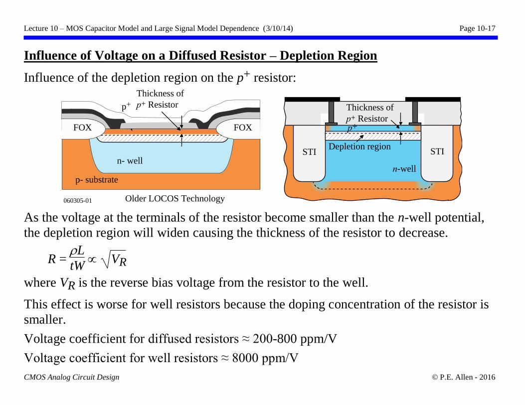
Influence of Voltage on a Diffused Resistor – Depletion Region
Influence of the depletion region on the p+ resistor:
As the voltage at the terminals of the resistor become smaller than the n-well potential,
the depletion region will widen causing the thickness of the resistor to decrease.
R = L
tW VR
where VR is the reverse bias voltage from the resistor to the well.
This effect is worse for well resistors because the doping concentration of the resistor is
smaller.
Voltage coefficient for diffused resistors ≈ 200-800 ppm/V
Voltage coefficient for well resistors ≈ 8000 ppm/V
060305-01
p- substrate
p+
Older LOCOS Technology
p+
n-well
STI STI
p+
Depletion region
Thickness of
p+ Resistor
n- well
FOX FOX
Thickness of
p+ Resistor
Lecture 10 – MOS Capacitor Model and Large Signal Model Dependence (3/10/14) Page 10-18
CMOS Analog Circuit Design © P.E. Allen - 2016
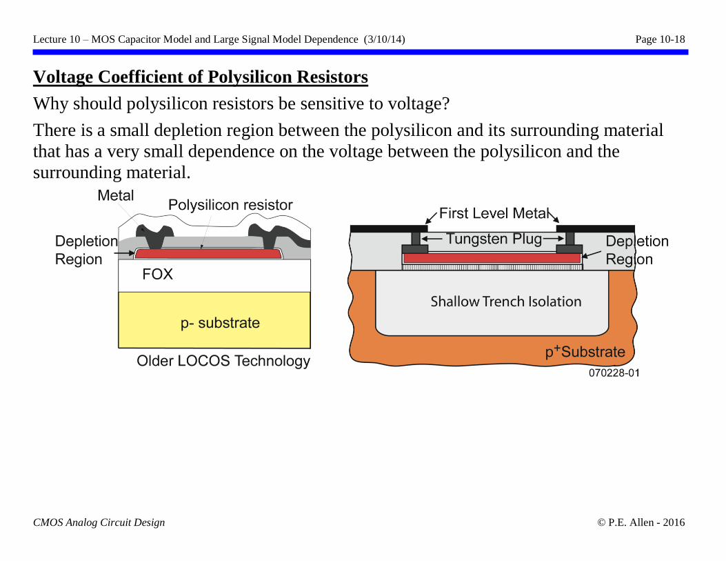
Voltage Coefficient of Polysilicon Resistors
Why should polysilicon resistors be sensitive to voltage?
There is a small depletion region between the polysilicon and its surrounding material
that has a very small dependence on the voltage between the polysilicon and the
surrounding material.
Lecture 10 – MOS Capacitor Model and Large Signal Model Dependence (3/10/14) Page 10-19
CMOS Analog Circuit Design © P.E. Allen - 2016
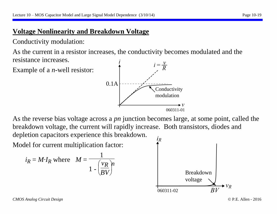
Voltage Nonlinearity and Breakdown Voltage
Conductivity modulation:
As the current in a resistor increases, the conductivity becomes modulated and the
resistance increases.
Example of a n-well resistor:
As the reverse bias voltage across a pn junction becomes large, at some point, called the
breakdown voltage, the current will rapidly increase. Both transistors, diodes and
depletion capacitors experience this breakdown.
Model for current multiplication factor:
iR = M·IR where M = 1
1 -
vR
BV
n
060311-01
i
v
i = vR
Conductivity
modulation
0.1A
060311-02
iR
vR
Breakdown
voltage
BV
Lecture 10 – MOS Capacitor Model and Large Signal Model Dependence (3/10/14) Page 10-20
CMOS Analog Circuit Design © P.E. Allen - 2016
DEPENDENCE OF THE LARGE SIGNAL MODEL ON TEMPERATURE
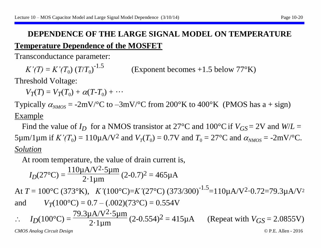
Temperature Dependence of the MOSFET
Transconductance parameter:
K’(T) = K’(T0) (T/T0)-1.5
(Exponent becomes +1.5 below 77°K)
Threshold Voltage:
VT(T) = VT(T0) + (T-T0) + ···
Typically NMOS = -2mV/°C to –3mV/°C from 200°K to 400°K (PMOS has a + sign)
Example
Find the value of ID for a NMOS transistor at 27°C and 100°C if VGS = 2V and W/L =
5µm/1µm if K’(T0) = 110µA/V2 and VT(T0) = 0.7V and T0 = 27°C and NMOS = -2mV/°C.
Solution
At room temperature, the value of drain current is,
ID(27°C) = 110µA/V2·5µm
2·1µm (2-0.7)2 = 465µA
At T = 100°C (373°K), K’(100°C)=K’(27°C) (373/300)-1.5
=110µA/V2·0.72=79.3µA/V2
and VT(100°C) = 0.7 – (.002)(73°C) = 0.554V
ID(100°C) = 79.3µA/V2·5µm
2·1µm (2-0.554)2 = 415µA (Repeat with VGS = 2.0855V)
Lecture 10 – MOS Capacitor Model and Large Signal Model Dependence (3/10/14) Page 10-21
CMOS Analog Circuit Design © P.E. Allen - 2016
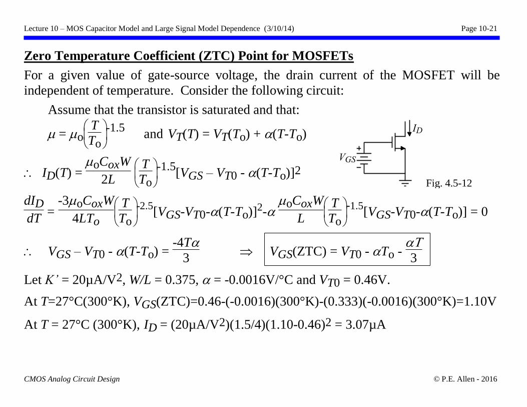
Zero Temperature Coefficient (ZTC) Point for MOSFETs
For a given value of gate-source voltage, the drain current of the MOSFET will be
independent of temperature. Consider the following circuit:
Assume that the transistor is saturated and that:
= o
T
To
-1.5 and VT(T) = VT(To) + (T-To)
ID(T) = oCoxW
2L
T
To
-1.5[VGS – VT0 - (T-To)]2
dIDdT
= -3oCoxW
4LTo
T
To
-2.5[VGS-VT0-(T-To)]2-
oCoxW
L
T
To
-1.5[VGS-VT0-(T-To)] = 0
VGS – VT0 - (T-To) = -4T
3 VGS(ZTC) = VT0 - To -
3
Let K’ = 20µA/V2, W/L = 0.375, = -0.0016V/°C and VT0 = 0.46V.
At T=27°C(300°K), VGS(ZTC)=0.46-(-0.0016)(300°K)-(0.333)(-0.0016)(300°K)=1.10V
At T = 27°C (300°K), ID = (20µA/V2)(1.5/4)(1.10-0.46)2 = 3.07µA
ID
VGS
Fig. 4.5-12
Lecture 10 – MOS Capacitor Model and Large Signal Model Dependence (3/10/14) Page 10-22
CMOS Analog Circuit Design © P.E. Allen - 2016
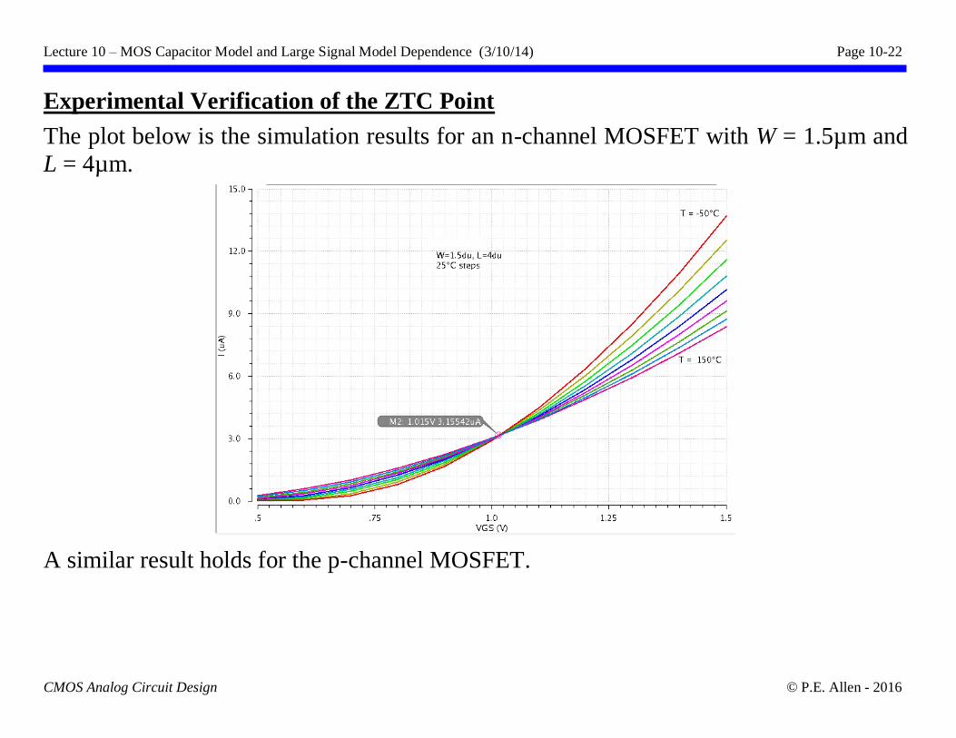
Experimental Verification of the ZTC Point
The plot below is the simulation results for an n-channel MOSFET with W = 1.5µm and
L = 4µm.
A similar result holds for the p-channel MOSFET.
Lecture 10 – MOS Capacitor Model and Large Signal Model Dependence (3/10/14) Page 10-23
CMOS Analog Circuit Design © P.E. Allen - 2016
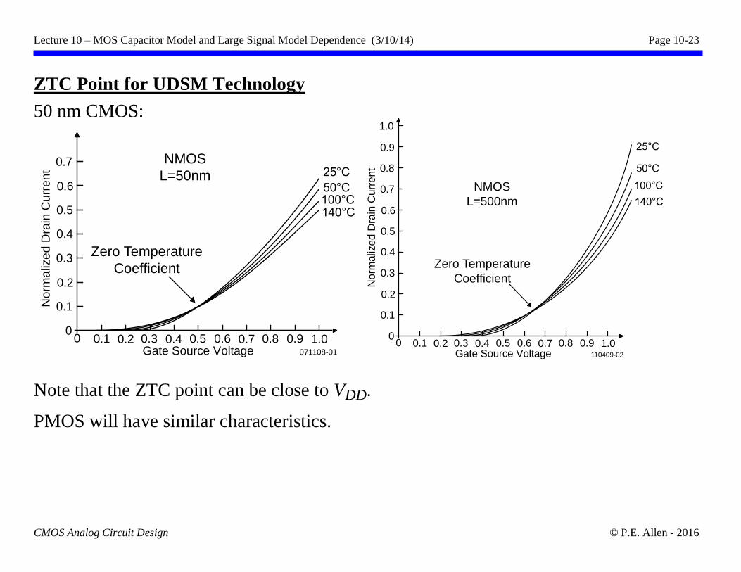
ZTC Point for UDSM Technology
50 nm CMOS:
Note that the ZTC point can be close to VDD.
PMOS will have similar characteristics.
0 0.1 0.2 0.3 0.4 0.5 0.6 0.7 0.8 0.9 1.0
0
0.1
0.2
0.3
0.4
0.5
0.6
0.7
Norm
aliz
ed D
rain
Cu
rre
nt
Gate Source Voltage
25°C
50°C100°C140°C
NMOS
L=50nm
Zero Temperature
Coefficient
071108-010 0.1 0.2 0.3 0.4 0.5 0.6 0.7 0.8 0.9 1.0
0
0.1
0.2
0.3
0.4
0.5
0.6
0.7
No
rmaliz
ed D
rain
Cu
rrent
Gate Source Voltage
25°C
50°C
100°C
140°C
NMOS
L=500nm
Zero Temperature
Coefficient
110409-02
0.8
0.9
1.0
Lecture 10 – MOS Capacitor Model and Large Signal Model Dependence (3/10/14) Page 10-24
CMOS Analog Circuit Design © P.E. Allen - 2016
Bulk-Drain (Bulk-Source) Leakage Currents
Cross-section of a NMOS in a p-well:
VGS>VT:
VGS<VT:
Polysilicon
p+
n- substrate
Fig.3.6-5
VG > VT VD > VDS(sat)
n+n+
Depletion
Region
B S
p-well
Polysilicon
p+
n- substrate
Fig.3.6-6
VG <VT VD > VDS(sat)
n+n+
Depletion
Region
B S
p-well
Lecture 10 – MOS Capacitor Model and Large Signal Model Dependence (3/10/14) Page 10-25
CMOS Analog Circuit Design © P.E. Allen - 2016
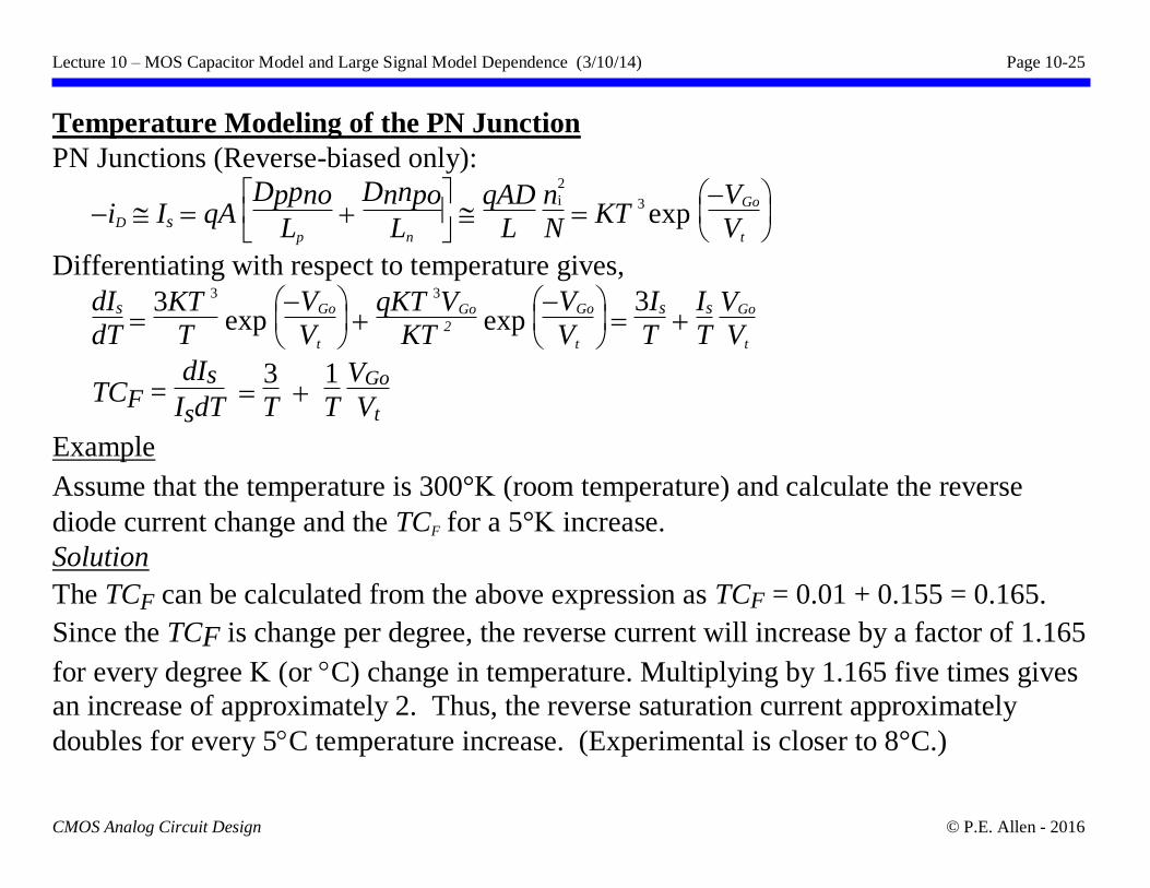
Temperature Modeling of the PN Junction
PN Junctions (Reverse-biased only):
−iD Is = qA
Dppno
Lp
+ Dnnpo
Ln
qAD
L n
2
i
N = KT
3 exp
−VGo
Vt
Differentiating with respect to temperature gives,
dIs
dT =
3KT 3
T exp
−VGo
Vt
+ qKT 3VGo
KT 2 exp
−VGo
Vt
= 3Is
T +
Is
T VGo
Vt
TCF = dIs
IsdT =
3
T +
1
T VGo
Vt
Example
Assume that the temperature is 300° (room temperature) and calculate the reverse
diode current change and the TCF for a 5° increase.
Solution
The TCF can be calculated from the above expression as TCF = 0.01 + 0.155 = 0.165.
Since the TCF is change per degree, the reverse current will increase by a factor of 1.165
for every degree (or C) change in temperature. Multiplying by 1.165 five times gives
an increase of approximately 2. Thus, the reverse saturation current approximately
doubles for every 5C temperature increase. (Experimental is closer to 8°C.)
Lecture 10 – MOS Capacitor Model and Large Signal Model Dependence (3/10/14) Page 10-26
CMOS Analog Circuit Design © P.E. Allen - 2016
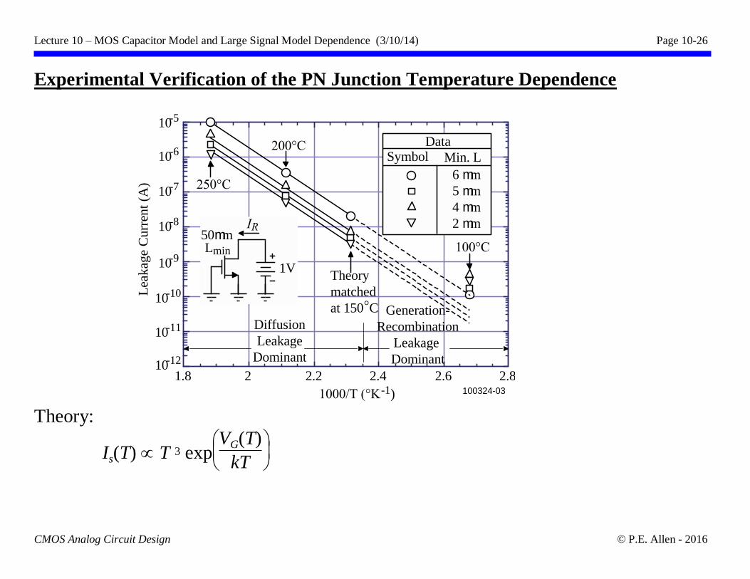
Experimental Verification of the PN Junction Temperature Dependence
Theory:
Is(T) T 3 exp
VG(T)
kT
10-12
10-11
10-10
10-9
10-8
10-7
10-6
10-5
1.8 2 2.2 2.4 2.6 2.8
1000/T (°K-1) 100324-03
Theory
matched
at 150°C
Symbol Min. L
Data
6 mm
5 mm
4 mm
2 mm
Generation-
Recombination
Leakage
Dominant
Diffusion
Leakage
Dominant
Lea
kag
e C
urr
ent
(A) 250°C
200°C
100°C
IR
1V
50mmLmin
Lecture 10 – MOS Capacitor Model and Large Signal Model Dependence (3/10/14) Page 10-27
CMOS Analog Circuit Design © P.E. Allen - 2016
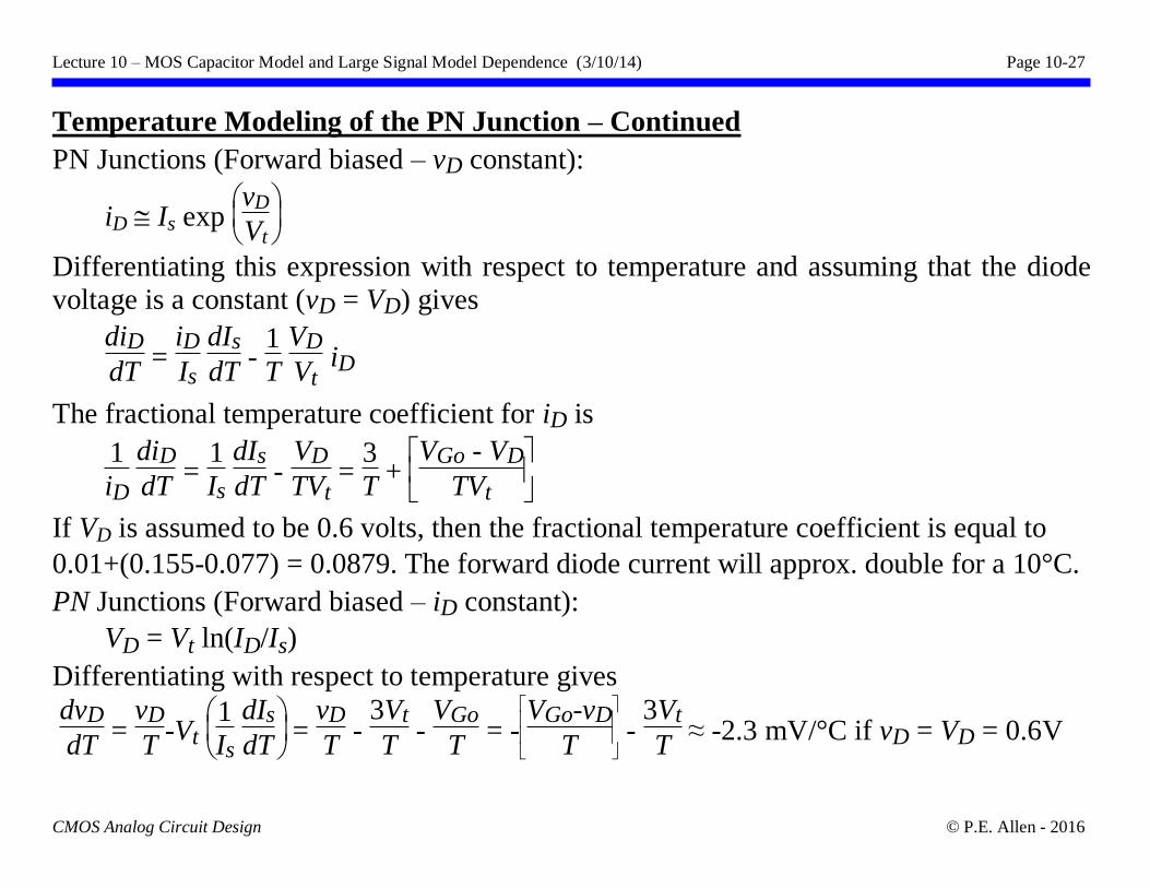
Temperature Modeling of the PN Junction – Continued
PN Junctions (Forward biased – vD constant):
iD Is exp
vD
Vt
Differentiating this expression with respect to temperature and assuming that the diode
voltage is a constant (vD = VD) gives
diDdT
= iDIs
dIs
dT -
1
T VD
Vt iD
The fractional temperature coefficient for iD is
1
iD diDdT
= 1
Is dIs
dT -
VD
TVt =
3
T +
VGo - VD
TVt
If VD is assumed to be 0.6 volts, then the fractional temperature coefficient is equal to
0.01+(0.155-0.077) = 0.0879. The forward diode current will approx. double for a 10°C.
PN Junctions (Forward biased – iD constant):
VD = Vt ln(ID/Is)
Differentiating with respect to temperature gives
dvD
dT =
vD
T-Vt
1
Is dIs
dT =
vD
T -
3Vt
T -
VGo
T = -
VGo-vD
T -
3Vt
T ≈ -2.3 mV/°C if vD = VD = 0.6V
Lecture 10 – MOS Capacitor Model and Large Signal Model Dependence (3/10/14) Page 10-28
CMOS Analog Circuit Design © P.E. Allen - 2016
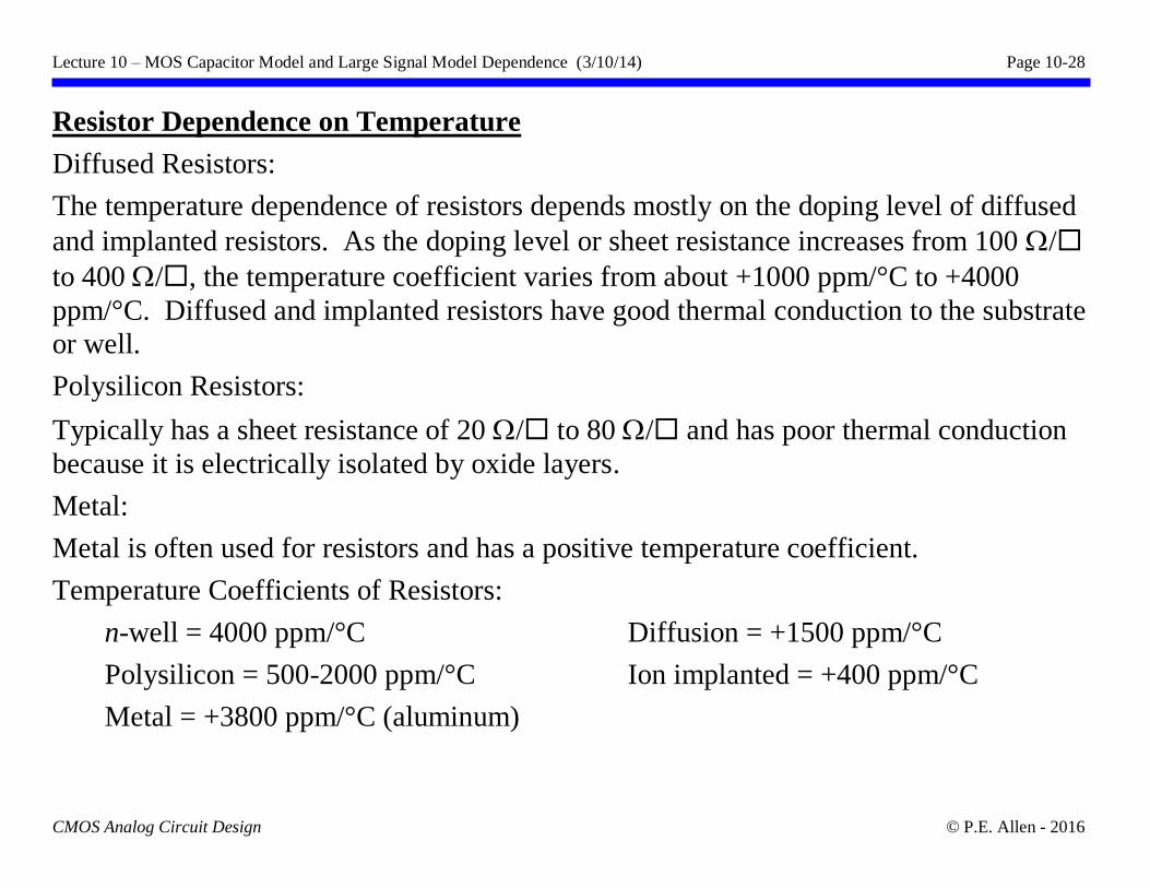
Resistor Dependence on Temperature
Diffused Resistors:
The temperature dependence of resistors depends mostly on the doping level of diffused
and implanted resistors. As the doping level or sheet resistance increases from 100 /
to 400 /, the temperature coefficient varies from about +1000 ppm/°C to +4000
ppm/°C. Diffused and implanted resistors have good thermal conduction to the substrate
or well.
Polysilicon Resistors:
Typically has a sheet resistance of 20 / to 80 / and has poor thermal conduction
because it is electrically isolated by oxide layers.
Metal:
Metal is often used for resistors and has a positive temperature coefficient.
Temperature Coefficients of Resistors:
n-well = 4000 ppm/°C Diffusion = +1500 ppm/°C
Polysilicon = 500-2000 ppm/°C Ion implanted = +400 ppm/°C
Metal = +3800 ppm/°C (aluminum)
Lecture 10 – MOS Capacitor Model and Large Signal Model Dependence (3/10/14) Page 10-29
CMOS Analog Circuit Design © P.E. Allen - 2016
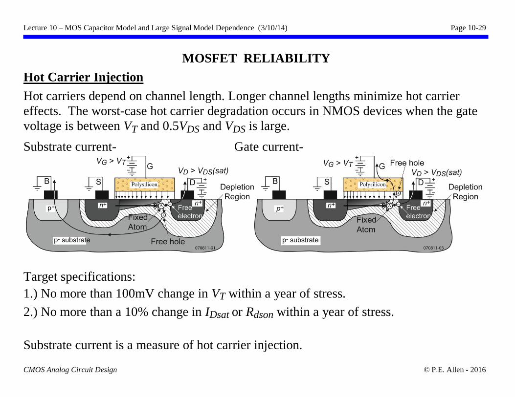
MOSFET RELIABILITY
Hot Carrier Injection
Hot carriers depend on channel length. Longer channel lengths minimize hot carrier
effects. The worst-case hot carrier degradation occurs in NMOS devices when the gate
voltage is between VT and 0.5VDS and VDS is large.
Substrate current- Gate current-
Target specifications:
1.) No more than 100mV change in VT within a year of stress.
2.) No more than a 10% change in IDsat or Rdson within a year of stress.
Substrate current is a measure of hot carrier injection.
Lecture 10 – MOS Capacitor Model and Large Signal Model Dependence (3/10/14) Page 10-30
CMOS Analog Circuit Design © P.E. Allen - 2016
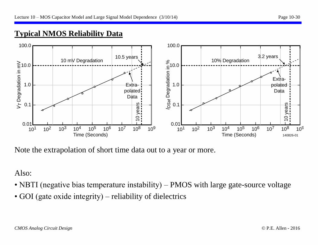
Typical NMOS Reliability Data
Note the extrapolation of short time data out to a year or more.
Also:
• NBTI (negative bias temperature instability) – PMOS with large gate-source voltage
• GOI (gate oxide integrity) – reliability of dielectrics
101 102 103 104 105 106 107 108 1090.01
0.1
1.0
10.0
100.0
VT D
eg
rada
tio
n in
mV
Time (Seconds)
Extra-
polated
Data
10 y
ea
rs
10 mV Degradation
101 102 103 104 105 106 107 108 1090.01
0.1
1.0
10.0
100.0
I DSat D
egra
datio
n in
%
Time (Seconds)
Extra-
polated
Data
10 y
ea
rs
10% Degradation10.5 years 3.2 years
140826-01
Lecture 10 – MOS Capacitor Model and Large Signal Model Dependence (3/10/14) Page 10-31
CMOS Analog Circuit Design © P.E. Allen - 2016
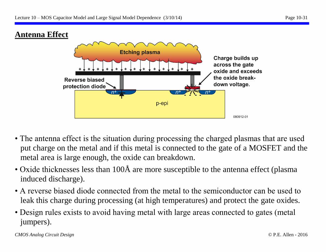
Antenna Effect
• The antenna effect is the situation during processing the charged plasmas that are used
put charge on the metal and if this metal is connected to the gate of a MOSFET and the
metal area is large enough, the oxide can breakdown.
• Oxide thicknesses less than 100Å are more susceptible to the antenna effect (plasma
induced discharge).
• A reverse biased diode connected from the metal to the semiconductor can be used to
leak this charge during processing (at high temperatures) and protect the gate oxides.
• Design rules exists to avoid having metal with large areas connected to gates (metal
jumpers).
Lecture 10 – MOS Capacitor Model and Large Signal Model Dependence (3/10/14) Page 10-32
CMOS Analog Circuit Design © P.E. Allen - 2016
SUMMARY
• The large signal capacitance model includes depletion and parallel plate capacitors
• The depletion capacitors CBD and CBS vary with their reverse bias voltage
• The capacitors CGD, CGS, and CGB have different values for the regions of cutoff,
active and saturated
• The large signal model varies with process primarily through µo and tox
• Voltage dependence of resistors and capacitors is primarily due to the influence of
depletion regions
• The temperature dependent large signal model of the MOSFET yields a gate-source
voltage where the derivative of drain current with respect to temperature is zero
• Other MOSFET temperature dependence comes from the leakage currents across
reverse biased pn junctions
• MOSFET reliability concerns degradation in performance over a specified lifetime


