Lecture 1 Introduction to Semiconductor Devices Reading: Notes
59
ECE 3080 - Dr. Alan Doolittle Georgia Tech Lecture 1 Introduction to Semiconductor Devices Reading: Notes and Anderson 2 Chapters 1.1-1.3, 1.7-1.9
Transcript of Lecture 1 Introduction to Semiconductor Devices Reading: Notes
ECE 3080 - Dr. Alan DoolittleGeorgia Tech
Lecture 1
Introduction to Semiconductor Devices
Reading:
Notes and Anderson2 Chapters 1.1-1.3, 1.7-1.9

ECE 3080 - Dr. Alan DoolittleGeorgia Tech
Atoms to Operational Amplifiers
•The goal of this course is to teach the fundamentals of non-linear circuit elements including diodes, LEDs, LASER diodes, transistors (BJT and FET) , and advanced device concepts such as microwave compound semiconductors and state of the art devices.•Due to the diverse coverage from various professors for ECE3040, you will repeat (for some) some of the material from 3040. Specifically, you will learn about the fundamentals of electron movement in semiconductor materials and develop this basic knowledge of how we can construct devices from these materials that can control the flow of electrons and light in useful ways.

ECE 3080 - Dr. Alan DoolittleGeorgia Tech
Market Study
Silicon is and will for a very long time be the dominant material used for electronics. However, MANY up and coming materials are slowly eating into silicon’s dominance.
Organic and compound semiconductors
Compound semiconductors
Compound semiconductors
ECE 3080 - Dr. Alan DoolittleGeorgia Tech
Devices we will study
Bold indicates devices covered in depth in ECE 3040
P-N diode, heterojunction diodes, ballistic diodes, Schottky barrier diodes, Metal-Semiconductor Contacts, LEDs, Lasers, Solar Cells, Photodetectors, BJT, HBT, MOSFET, MESFET, JFET, Polarization Based Devices (III-Nitrides HEMTs and Ferroelectric transistors), CCD, Microwave transistors, power transistors, organic semiconductors
ECE 3080 - Dr. Alan DoolittleGeorgia Tech
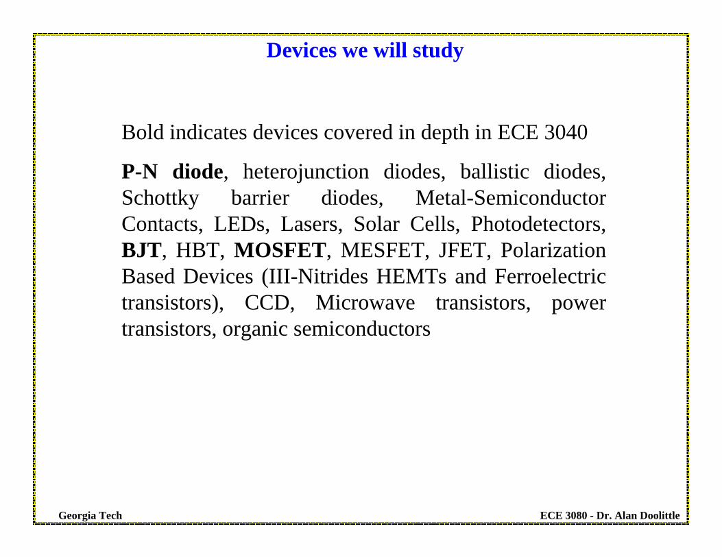
Modern amplifiers consist of extremely small devices
Transistors in the above image are only a few microns (µm or 1e-6 meters) on a side.
Modern devices have lateral dimensions that are only fractions of a micron (~0.1 µm) and vertical dimensions that may be only a few atoms tall.

ECE 3080 - Dr. Alan DoolittleGeorgia Tech
Intel Develops World's Smallest, Fastest CMOS TransistorSANTA CLARA, Calif., Dec. 11, 2000 - Intel Corporation researchers have achieved a significant breakthrough by building the
world's smallest and fastest CMOS transistor. This breakthrough will allow Intel within the next five to 10 years to build microprocessors containing more than 400 million transistors, running at 10 gigahertz (10 billion cycles per second) and operating at less than one volt.
The transistors feature structures just 30 nanometers in size and three atomic layers thick. (Note: A nanometer is one-billionth of a meter). Smaller transistors are faster, and fast transistors are the key building block for fast microprocessors, the brains of computers and countless other smart devices.
These new transistors, which act like switches controlling the flow of electrons inside a microchip, could complete 400 million calculations in the blink an eye or finish two million calculations in the time it takes a speeding bullet to travel one inch.
Scientists expect such powerful microprocessors to allow applications popular in science-fiction stories -- such as instantaneous, real-time voice translation -- to become an everyday reality.
Researchers from Intel Labs are disclosing the details of this advance today in San Francisco at the International Electron Devices Meeting, the premier technical conference for semiconductor engineers and scientists.
"This breakthrough will allow Intel to continue increasing the performance and reducing the cost of microprocessors well into the future," said Dr. Sunlin Chou, vice president and general manager of Intel's Technology and Manufacturing Group. "As our researchers venture into uncharted areas beyond the previously expected limits of silicon scaling, they find Moore's Law still intact."
Intel researchers were able to build these ultra-small transistors by aggressively reducing all of their dimensions. The gate oxides used to build these transistors are just three atomic layers thick. More than 100,000 of these gates would need to be stacked to achieve the thickness of a sheet of paper. Also significant is that these experimental transistors, while featuring capabilities that are generations beyond the most advanced technologies used in manufacturing today, were built using the same physical structure as in today's computer chips.
"Many experts thought it would be impossible to build CMOS transistors this small because of electrical leakage problems," notedDr. Gerald Marcyk, director of Intel's Components Research Lab, Technology and Manufacturing Group. "Our research proves that these smaller transistors behave in the same way as today's devices and shows there are no fundamental barriers to producing these devices in high volume in the future. The most important thing about these 30 nanometer transistors is that they are simultaneously small and fast, and work at low voltage. Typically you can achieve two of the three, but delivering on all facets is a significant accomplishment."
“It's discoveries like these that make me excited about the future," added Chou. "It's one thing to achieve a great technologicalbreakthrough. It's another to have one that is practical and will change everyone's lives. With Intel's 30 nanometer transistor, we have both."
For more information on Intel Silicon Technology Research, please reference Intel's new Silicon Showcase at www.intel.com/research/silicon. Intel, the world's largest chip maker, is also a leading manufacturer of computer, networking and communications products. Additional information about Intel is available at www.intel.com/pressroom. Source: Intel Web Page.
Famous Last Words: “I only want to design computers. I do not need to know about ‘atoms and electrons’ ”. --- A Doomed Computer Engineer

ECE 3080 - Dr. Alan DoolittleGeorgia Tech
•Conductivity, σ, is the ease with which a given material conducts electricity.
•Ohms Law: V=IR or J=σE where J is current density and E is electric field.
•Metals: High conductivity
•Insulators: Low Conductivity
•Semiconductors: Conductivity can be varied by several orders of magnitude.
•It is the ability to control conductivity that make semiconductors useful as “current/voltage control elements”. “Current/Voltage control” is the key to switches (digital logic including microprocessors etc…), amplifiers, LEDs, LASERs, photodetectors, etc...
Control of Conductivity is the Key to Modern Electronic Devices
ECE 3080 - Dr. Alan DoolittleGeorgia Tech
Electrical/Computer engineers like to classify materials based on electrical behavior (insulating, semi-insulating, and metals).
Materials Engineers/Scientists classify materials based on bond type (covalent, ionic, metallic, or van der Waals), or structure (crystalline, polycrystalline, amorphous, etc...).
In 20-50 years, EE’s may not be using semiconductors at all!! Polymers or bio-electronics may replace them! However the materials science will be the same!
Classifications of Electronic Materials

ECE 3080 - Dr. Alan DoolittleGeorgia Tech
•For metals, the electrons can jump from the valence orbits (outermost core energy levels of the atom) to any position within the crystal (free to move throughout the crystal) with no “extra energy needed to be supplied”•For insulators, it is VERY DIFFICULT for the electrons to jump from the valence orbits and requires a huge amount of energy to “free the electron” from the atomic core.•For semiconductors, the electrons can jump from the valence orbits but does require a small amount of energy to “free the electron” from the atomic core.
Classifications of Electronic Materials

ECE 3080 - Dr. Alan DoolittleGeorgia Tech
•Semiconductor materials are a sub-class of materials distinguished by the existence of a range of disallowed energies between the energies of the valence electrons (outermost core electrons) and the energies of electrons free to move throughout the material.•The energy difference (energy gap or bandgap) between the states in which the electron is bound to the atom and when it is free to conduct throughout the crystal is related to the bonding strength of the material, it’s density, the degree of ionicity of the bond, and the chemistry related to the valence of bonding.•High bond strength materials (diamond, SiC, AlN, GaN etc...) tend to have large energy bandgaps.•Lower bond strength materials (Si, Ge, etc...) tend to have smaller energy bandgaps.
Classifications of Electronic Materials

ECE 3080 - Dr. Alan DoolittleGeorgia Tech
Classifications of Electronic Materials
•More formally, the energy gap is derived from the Pauli exclusion principle, where no two electrons occupying the same space, can have the same energy. Thus, as atoms are brought closer towards one another and begin to bond together, their energy levels must split into bands of discrete levels so closely spaced in energy, they can be considered a continuum of allowed energy. •Strongly bonded materials tend to have small interatomic distances between atoms. Thus, the strongly bonded materials can have larger energy bandgaps than do weakly bonded materials.
ECE 3080 - Dr. Alan DoolittleGeorgia Tech
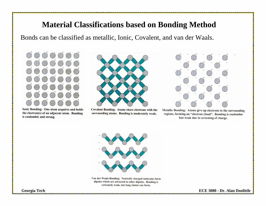
Material Classifications based on Bonding MethodBonds can be classified as metallic, Ionic, Covalent, and van der Waals.

ECE 3080 - Dr. Alan DoolittleGeorgia Tech
Consider the case of the group 4 elements, all** covalently bonded
Element Atomic Radius/Lattice Constant Bandgap(How closely spaced are the atoms?)
C 0.91/3.56 Angstroms 5.47 eV
Si 1.46/5.43 Angstroms 1.12 eV
Ge 1.52/5.65 Angstroms 0.66 eV
α-Sn 1.72/6.49 Angstroms ~0.08 eV*
Pb 1.81/** Angstroms Metal
*Only has a measurable bandgap near 0K
**Different bonding/Crystal Structure due to unfilled higher orbital states

ECE 3080 - Dr. Alan DoolittleGeorgia Tech
Classifications of Electronic MaterialsTypes of Semiconductors:•Elemental: Silicon or Germanium (Si or Ge)•Compound: Gallium Arsenide (GaAs), Indium Phosphide (InP), Silicon Carbide (SiC), CdS and many others
•Note that the sum of the valence adds to 8, a complete outer shell. I.E. 4+4, 3+5, 2+6, etc...

ECE 3080 - Dr. Alan DoolittleGeorgia Tech
Compound Semiconductors: Offer high performance (optical characteristics, higher frequency, higher power) than elemental semiconductors and greater device design flexibility due to mixing of materials.
Binary: GaAs, SiC, etc...
Ternary: AlxGa1-xAs, InxGa1-xN where 0<=x<=1
Quaternary: InxGa1-xAsyP1-y where 0<=x<=1 and 0<=y<=1
Half the total number of atoms must come from group III (Column III) and the other half the atoms must come from group V (Column V) (or more precisely, IV/IV , III/V, or II/VI combinations) leading to the above “reduced semiconductor notation.
Example: Assume a compound semiconductor has 25% “atomic”concentrations of Ga, 25% “atomic” In and 50% “atomic” of N. The chemical formula would be:
Ga0.25In0.25N0.5
But the correct reduced semiconductor formula would be:
Ga0.5In0.5N
Classifications of Electronic Materials

ECE 3080 - Dr. Alan DoolittleGeorgia Tech
Material Classifications based on Crystal Structure
Amorphous MaterialsNo discernible long range atomic order (no detectable crystal structure). Examples are silicon
dioxide (SiO2), amorphous-Si, silicon nitride (Si3N4), and others. Though usually thought of as less perfect than crystalline materials, this class of materials is extremely useful.Polycrystalline Materials
Material consisting of several “domains” of crystalline material. Each domain can be oriented differently than other domains. However, within a single domain, the material is crystalline. The size of the domains may range from cubic nanometers to several cubic centimeters. Many semiconductors are polycrystalline as are most metals.
Crystalline MaterialsCrystalline materials are characterized by an atomic symmetry that repeats spatially. The shape of
the unit cell depends on the bonding of the material. The most common unit cell structures are diamond, zincblende (a derivative of the diamond structure), hexagonal, and rock salt (simple cubic).
Classifications of Electronic Materials

ECE 3080 - Dr. Alan DoolittleGeorgia Tech
Chemical Vapor Deposition
Chemical gas sources are thermally, optically, or electrically (plasma) reacted with a surface to “leave” behind deposits with reaction byproducts pumped out of the reaction tube or vacuum chamber.
ECE 3080 - Dr. Alan DoolittleGeorgia Tech
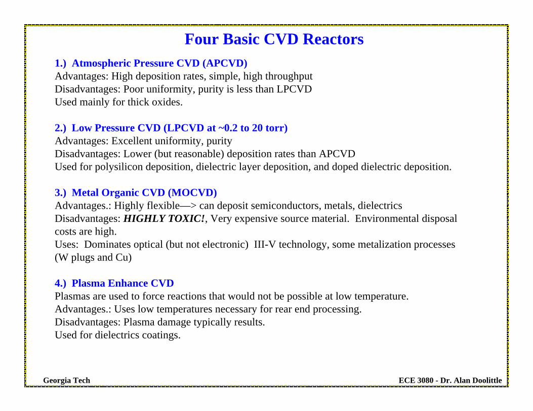
1.) Atmospheric Pressure CVD (APCVD)Advantages: High deposition rates, simple, high throughputDisadvantages: Poor uniformity, purity is less than LPCVDUsed mainly for thick oxides.
2.) Low Pressure CVD (LPCVD at ~0.2 to 20 torr)Advantages: Excellent uniformity, purityDisadvantages: Lower (but reasonable) deposition rates than APCVDUsed for polysilicon deposition, dielectric layer deposition, and doped dielectric deposition.
3.) Metal Organic CVD (MOCVD)Advantages.: Highly flexible—> can deposit semiconductors, metals, dielectricsDisadvantages: HIGHLY TOXIC!, Very expensive source material. Environmental disposal costs are high.Uses: Dominates optical (but not electronic) III-V technology, some metalization processes (W plugs and Cu)
4.) Plasma Enhance CVDPlasmas are used to force reactions that would not be possible at low temperature.Advantages.: Uses low temperatures necessary for rear end processing. Disadvantages: Plasma damage typically results.Used for dielectrics coatings.
Four Basic CVD Reactors

ECE 3080 - Dr. Alan DoolittleGeorgia Tech
LPCVD of OxidesUses:Undoped: Insulator between multilevel metalization, implantation or diffusion mask, increase thermal oxide thickness for high voltage devices.Doped: P-doped is used as a multilevel metalization insulator, final passivation layer (prevents ionic diffusion), or a gettering source.
Undoped Oxide Deposition Methods:Silane SiH4 + O2 —> SiO2 + 2H2 < 500 °C (contain H2O, SiH, and SiOH impurities)DCS (Dichlorosilane) SiCl2H2 + 2N2O —> SiO2 + 2N2 + 2HCL (etches) ~900 °C (contains Cl)TEOS (tetraethoxysilane) Si(OC2H5)4 —> SiO2 + many byproducts 650-750 °CTEOS + Ozone (O3) Ozone is more reactive and lowers deposition temperatures to ~400 °C

ECE 3080 - Dr. Alan DoolittleGeorgia Tech
Doped Oxide Deposition Methods:PSG - Phosphorosilicate Glass4PH3 + 5O2 ----> 2P2O5 + 6H2 ~950-1100 °C for flowed glass and <400 for passivation
BPSG - Borophosphorosilicate GlassPH3 + B2H6 + O2 —> Complex BXPYOZ ~850-950 °C , Flows better than PSG, but can absorb moisture
Doped Oxides (glasses) can be made to “flow” or smooth out. This is particularly useful for smooth interconnects (prevents sharp edges which tend to break metal lines) or for partial global planarization for subsequent lithography steps.
LPCVD of Doped Oxides

ECE 3080 - Dr. Alan DoolittleGeorgia Tech
Single Crystal Semiconductors (Epitaxy)
We can grow* crystalline semiconductors by raising the temperature to allow more surface migration and by using a crystalline substrate (Si, GaAs, InP wafer, etc…)===> Single crystal material mimicking the crystal structure of the layers below it.
Epitaxy
*Instead of the word deposit, we use “grow” to describe the tendency of the deposited material to mimic the crystal structure of crystalline substrate material.
ECE 3080 - Dr. Alan DoolittleGeorgia Tech
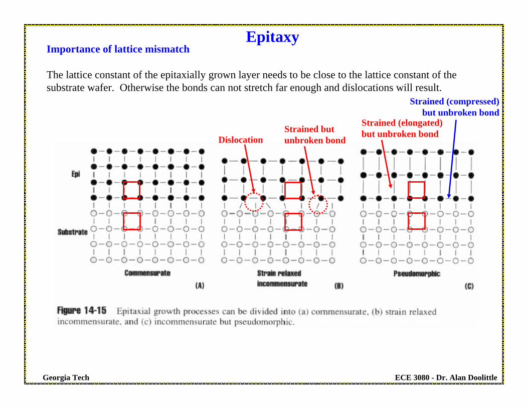
EpitaxyImportance of lattice mismatch
The lattice constant of the epitaxially grown layer needs to be close to the lattice constant of the substrate wafer. Otherwise the bonds can not stretch far enough and dislocations will result.
DislocationStrained but unbroken bond
Strained (elongated) but unbroken bond
Strained (compressed) but unbroken bond

ECE 3080 - Dr. Alan DoolittleGeorgia Tech
EpitaxyImportance of lattice mismatch
The lattice constant of the epitaxially grown layer needs to be close to the lattice constant of the substrate wafer. Otherwise the bonds can not stretch far enough and dislocations will result.

ECE 3080 - Dr. Alan DoolittleGeorgia Tech
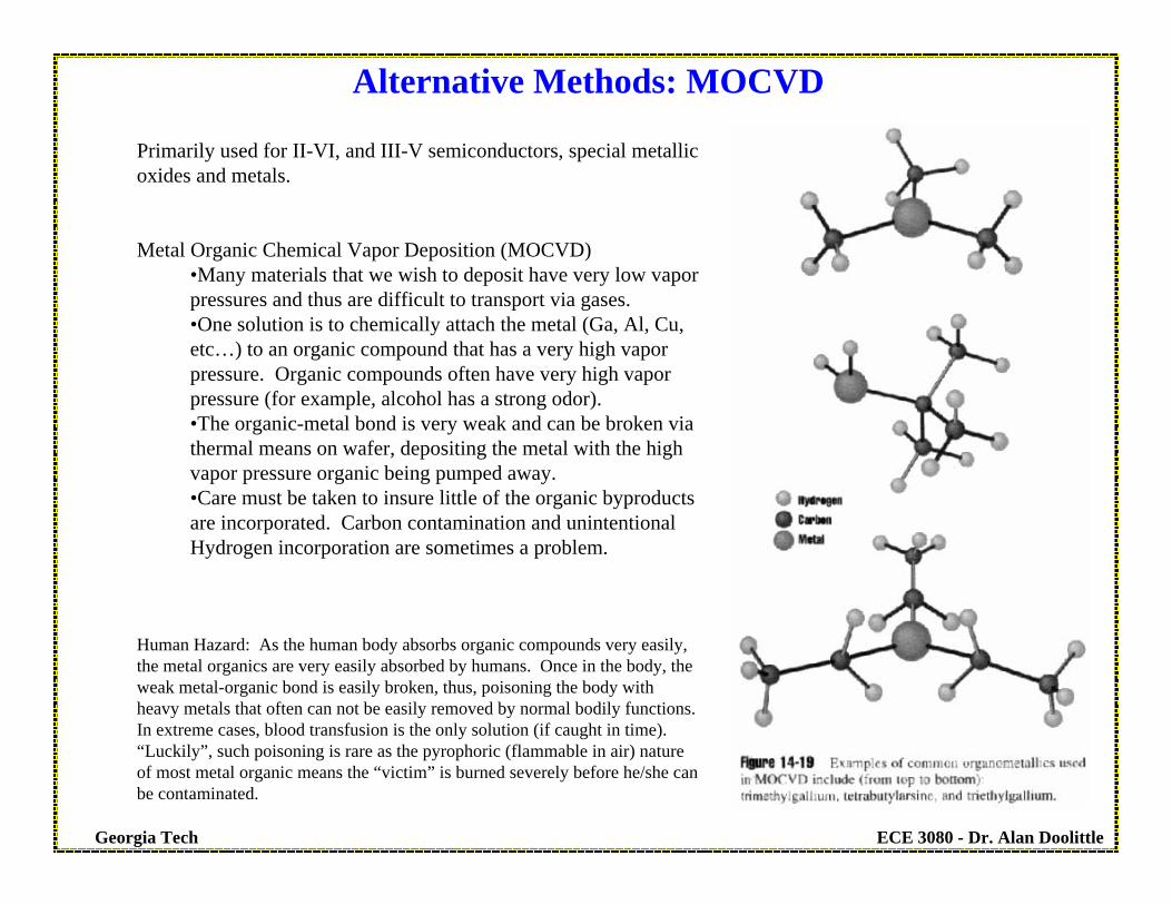
Primarily used for II-VI, and III-V semiconductors, special metallic oxides and metals.
Metal Organic Chemical Vapor Deposition (MOCVD)•Many materials that we wish to deposit have very low vapor pressures and thus are difficult to transport via gases.•One solution is to chemically attach the metal (Ga, Al, Cu, etc…) to an organic compound that has a very high vapor pressure. Organic compounds often have very high vapor pressure (for example, alcohol has a strong odor).•The organic-metal bond is very weak and can be broken via thermal means on wafer, depositing the metal with the high vapor pressure organic being pumped away.•Care must be taken to insure little of the organic byproducts are incorporated. Carbon contamination and unintentional Hydrogen incorporation are sometimes a problem.
Human Hazard: As the human body absorbs organic compounds very easily, the metal organics are very easily absorbed by humans. Once in the body, the weak metal-organic bond is easily broken, thus, poisoning the body with heavy metals that often can not be easily removed by normal bodily functions. In extreme cases, blood transfusion is the only solution (if caught in time).
MOCVD

ECE 3080 - Dr. Alan DoolittleGeorgia Tech
Commercial Thomas Swan® MOCVD

ECE 3080 - Dr. Alan DoolittleGeorgia Tech
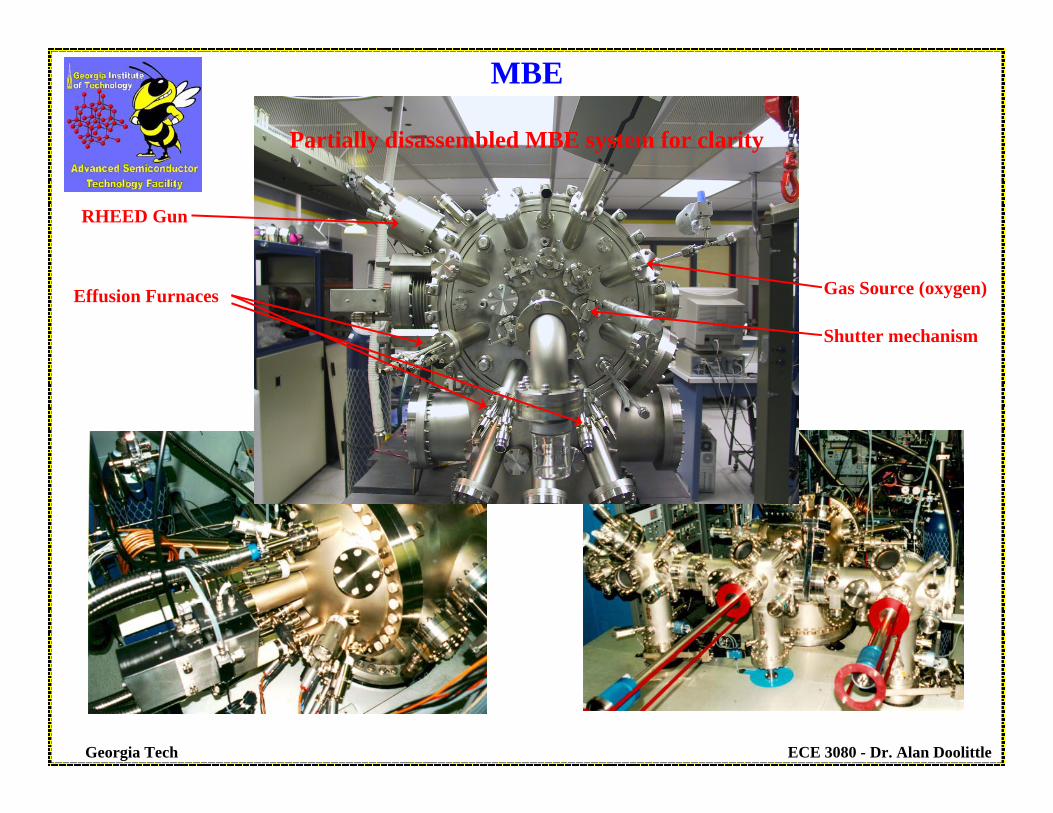
Molecular Beam Epitaxy (MBE)Dominates III-V electronic market and strong competitor in upper end LASER marketOffers the highest purity material (due to UHV conditions) and the best layer control (almost any fraction of an atomic layer can be deposited and layers can be sequenced one layer at a time (for example Ga then As then Ga etc…).
MBE
•In an UHV chamber, ultra high purity materials are evaporated.•Because of the very low pressure, the mean free path is very long (can be hundreds of meters). Thus, the evaporated material travels in a straight line (a molecular beam) toward a hot substrate.•Once on the substrate, the atom or molecule moves around until it finds an atomic site to chemically bond to.•Shutters can be used to turn the beam flux on and off•The flux of atoms/molecules is controlled by the temperature of the “effusion cell”(evaporation source).
ECE 3080 - Dr. Alan DoolittleGeorgia Tech
MBE
Effusion Furnaces
Partially disassembled MBE system for clarity
RHEED Gun
Gas Source (oxygen)
Shutter mechanism
ECE 3080 - Dr. Alan DoolittleGeorgia Tech
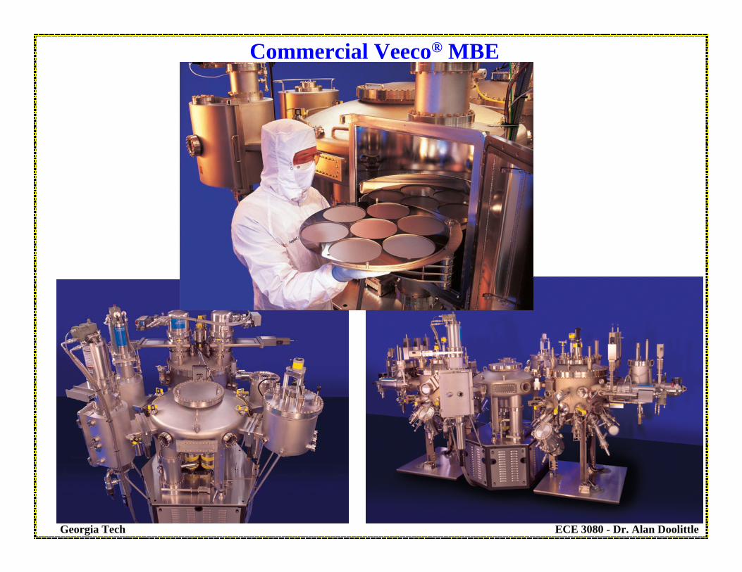
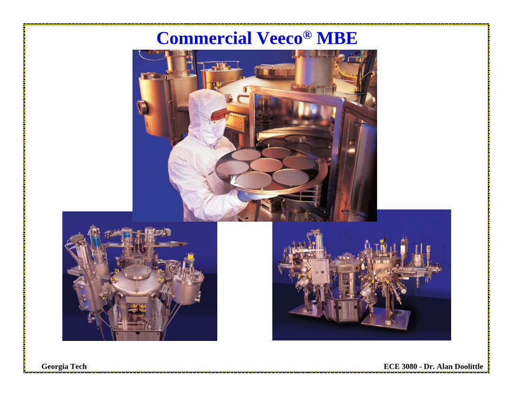
Commercial Veeco® MBE

ECE 3080 - Dr. Alan DoolittleGeorgia Tech
Molecular Beam Epitaxy (MBE)

ECE 3080 - Dr. Alan DoolittleGeorgia Tech
Molecular Beam Epitaxy (MBE)

ECE 3080 - Dr. Alan DoolittleGeorgia Tech
Crystalline Order
Water Molecules, H2O, forming “Snowflakes”Atoms forming a “Semiconductor”
Need two volunteers… (demo on how a crystal forms naturally due to
repulsive electronic bonds)
ECE 3080 - Dr. Alan DoolittleGeorgia Tech
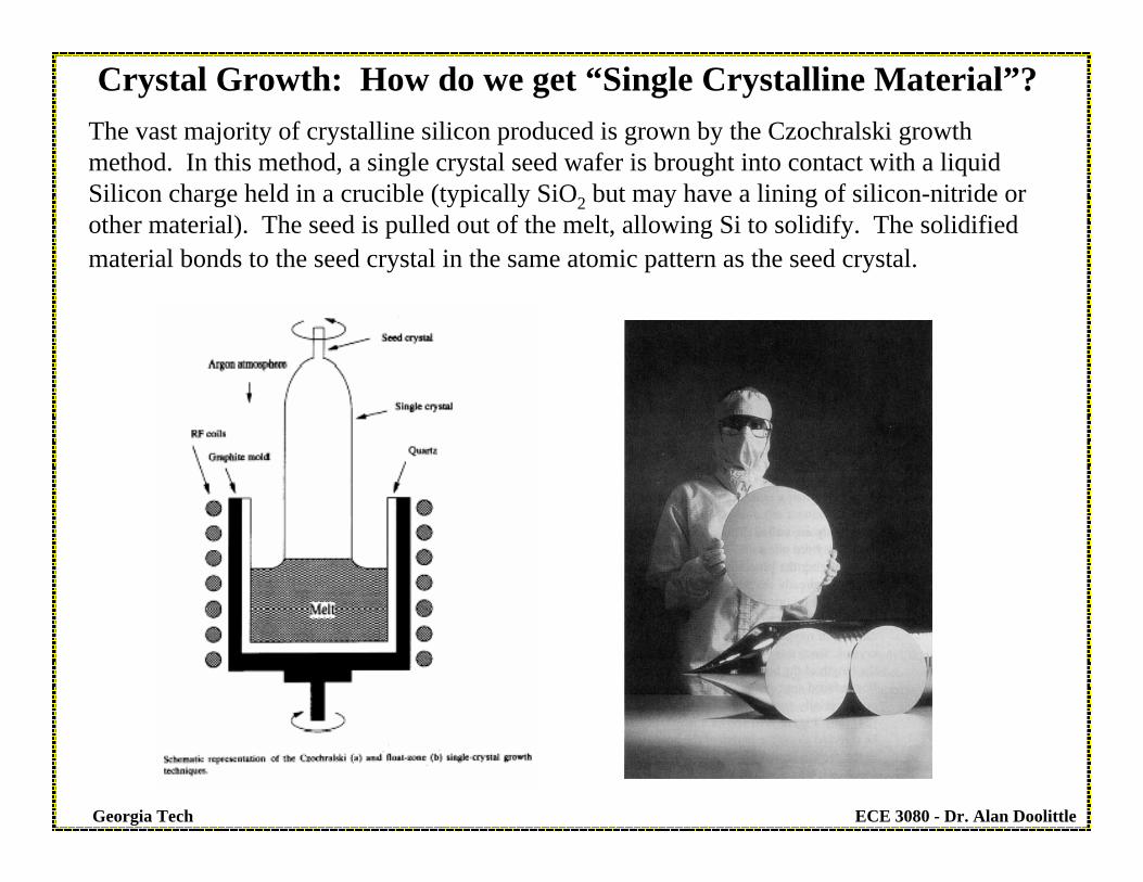
Crystal Growth: How do we get “Single Crystalline Material”?The vast majority of crystalline silicon produced is grown by the Czochralski growth method. In this method, a single crystal seed wafer is brought into contact with a liquid Silicon charge held in a crucible (typically SiO2 but may have a lining of silicon-nitride or other material). The seed is pulled out of the melt, allowing Si to solidify. The solidified material bonds to the seed crystal in the same atomic pattern as the seed crystal.
ECE 3080 - Dr. Alan DoolittleGeorgia Tech
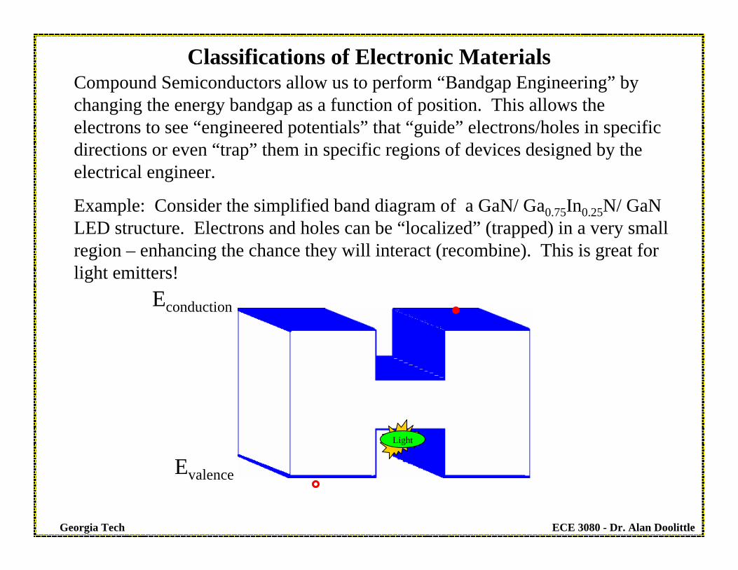
Compound Semiconductors allow us to perform “Bandgap Engineering” by changing the energy bandgap as a function of position. This allows the electrons to see “engineered potentials” that “guide” electrons/holes in specific directions or even “trap” them in specific regions of devices designed by the electrical engineer.
Example: Consider the simplified band diagram of a GaN/ Ga0.75In0.25N/ GaN LED structure. Electrons and holes can be “localized” (trapped) in a very small region – enhancing the chance they will interact (recombine). This is great for light emitters!
Classifications of Electronic Materials
Econduction
Evalence
Light
ECE 3080 - Dr. Alan DoolittleGeorgia Tech
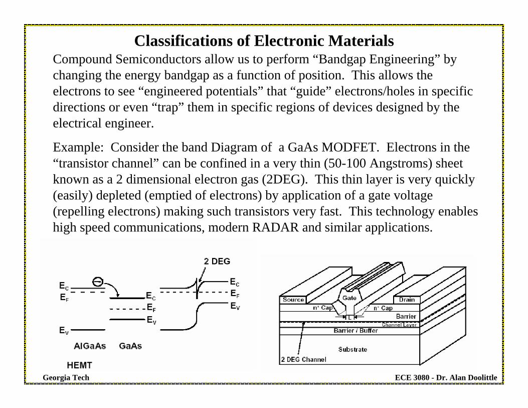
Compound Semiconductors allow us to perform “Bandgap Engineering” by changing the energy bandgap as a function of position. This allows the electrons to see “engineered potentials” that “guide” electrons/holes in specific directions or even “trap” them in specific regions of devices designed by the electrical engineer.
Example: Consider the band Diagram of a GaAs MODFET. Electrons in the “transistor channel” can be confined in a very thin (50-100 Angstroms) sheet known as a 2 dimensional electron gas (2DEG). This thin layer is very quickly (easily) depleted (emptied of electrons) by application of a gate voltage (repelling electrons) making such transistors very fast. This technology enables high speed communications, modern RADAR and similar applications.
Classifications of Electronic Materials
ECE 3080 - Dr. Alan DoolittleGeorgia Tech
How do we produce these Energy Engineered Structures and Devices?
Epitaxial Semiconductor and Dielectric deposition Techniques:•“Epitaxial” is derived from the Greek word for skin, more specifically “thin skin”. Thin layers of materials are deposited on a substrate
•Temperature and substrate determines the physical structure of the deposited films:
•Low Temperatures or non-crystalline substrate:
•Materials end up with amorphous or polycrystalline materials
•High Temperature AND Crystalline substrate
•Need to have an existing crystalline wafer so as to “seed” the crystallization process.
•Films that retain the substrates basic crystal structure are “Epitaxial”
ECE 3080 - Dr. Alan DoolittleGeorgia Tech
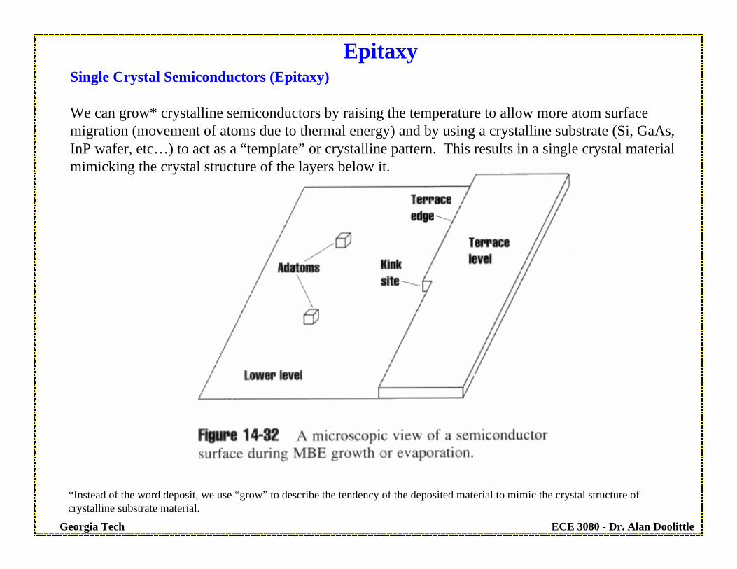
Single Crystal Semiconductors (Epitaxy)
We can grow* crystalline semiconductors by raising the temperature to allow more atom surface migration (movement of atoms due to thermal energy) and by using a crystalline substrate (Si, GaAs, InP wafer, etc…) to act as a “template” or crystalline pattern. This results in a single crystal material mimicking the crystal structure of the layers below it.
Epitaxy
*Instead of the word deposit, we use “grow” to describe the tendency of the deposited material to mimic the crystal structure of crystalline substrate material.

ECE 3080 - Dr. Alan DoolittleGeorgia Tech
Advanced Semiconductor Technology Facility
Dr. W. Alan Doolittle
Contact Information:Phone and Fax: 404-894-9884Email: [email protected]: School of Electrical and Computer EngineeringGeorgia Institute of Technology777 Atlantic Dr.Atlanta, GA 30332-0250
ECE 3080 - Dr. Alan DoolittleGeorgia Tech
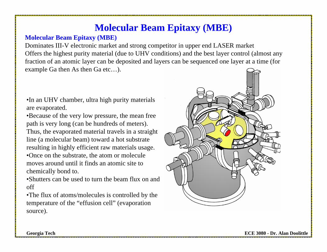
Molecular Beam Epitaxy (MBE)Dominates III-V electronic market and strong competitor in upper end LASER marketOffers the highest purity material (due to UHV conditions) and the best layer control (almost any fraction of an atomic layer can be deposited and layers can be sequenced one layer at a time (for example Ga then As then Ga etc…).
Molecular Beam Epitaxy (MBE)
•In an UHV chamber, ultra high purity materials are evaporated.•Because of the very low pressure, the mean free path is very long (can be hundreds of meters). Thus, the evaporated material travels in a straight line (a molecular beam) toward a hot substrate resulting in highly efficient raw materials usage.•Once on the substrate, the atom or molecule moves around until it finds an atomic site to chemically bond to.•Shutters can be used to turn the beam flux on and off•The flux of atoms/molecules is controlled by the temperature of the “effusion cell” (evaporation source).

ECE 3080 - Dr. Alan DoolittleGeorgia Tech
Molecular Beam Epitaxy (MBE)

ECE 3080 - Dr. Alan DoolittleGeorgia Tech
Molecular Beam Epitaxy (MBE)

ECE 3080 - Dr. Alan DoolittleGeorgia Tech
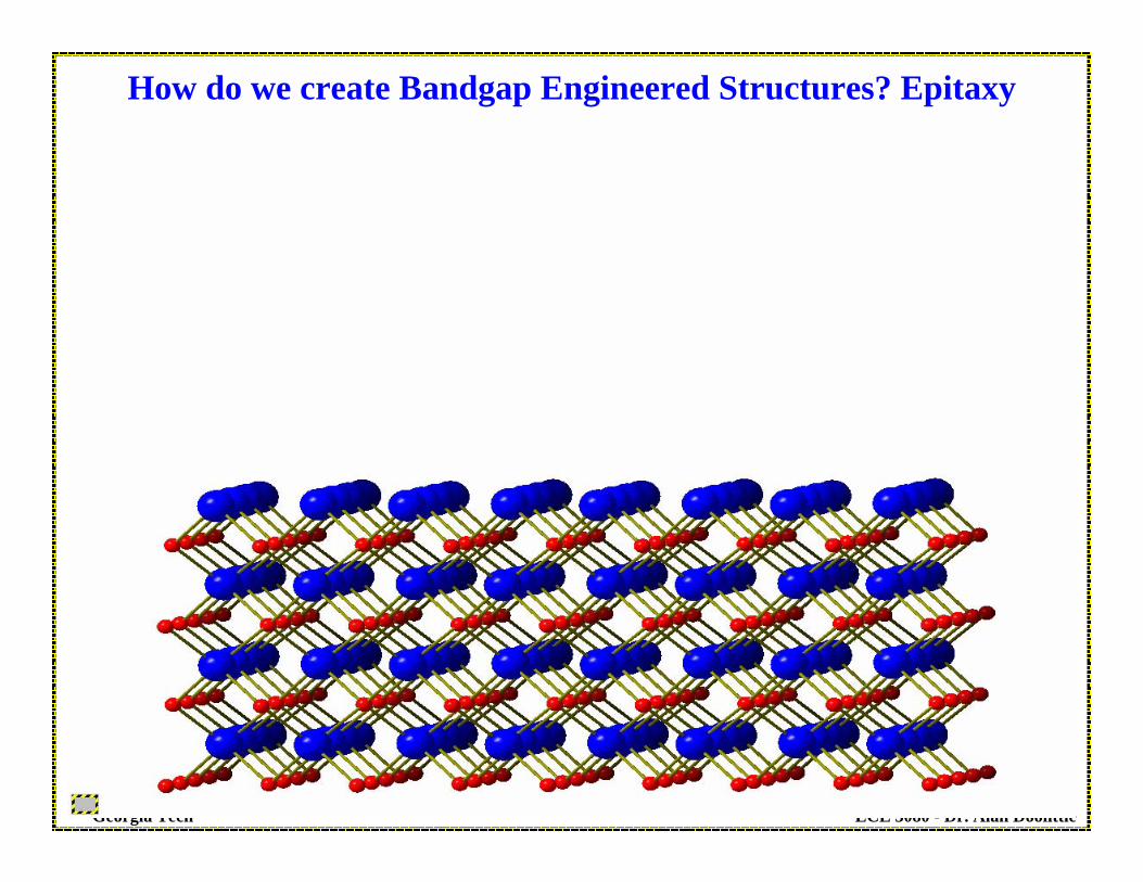
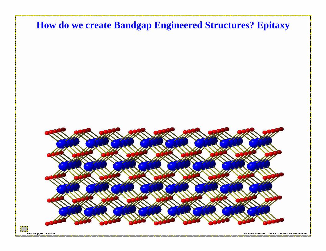
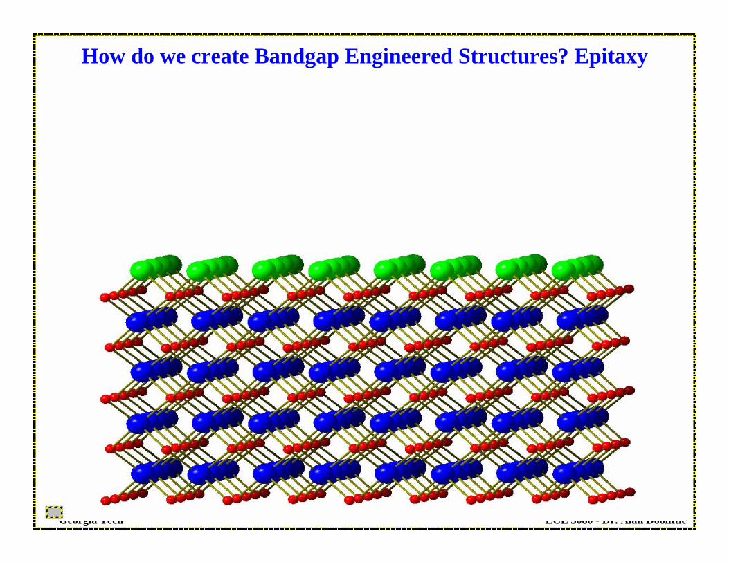
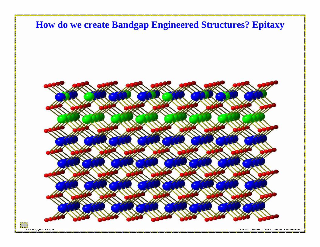
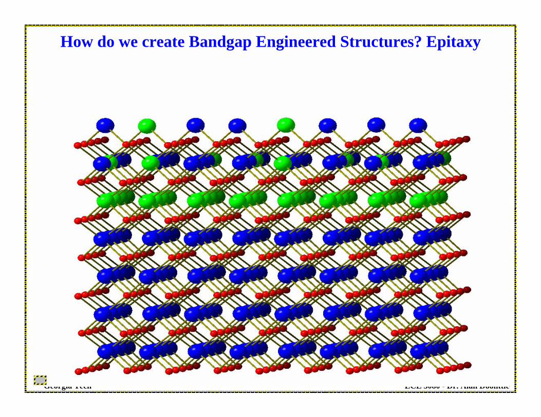
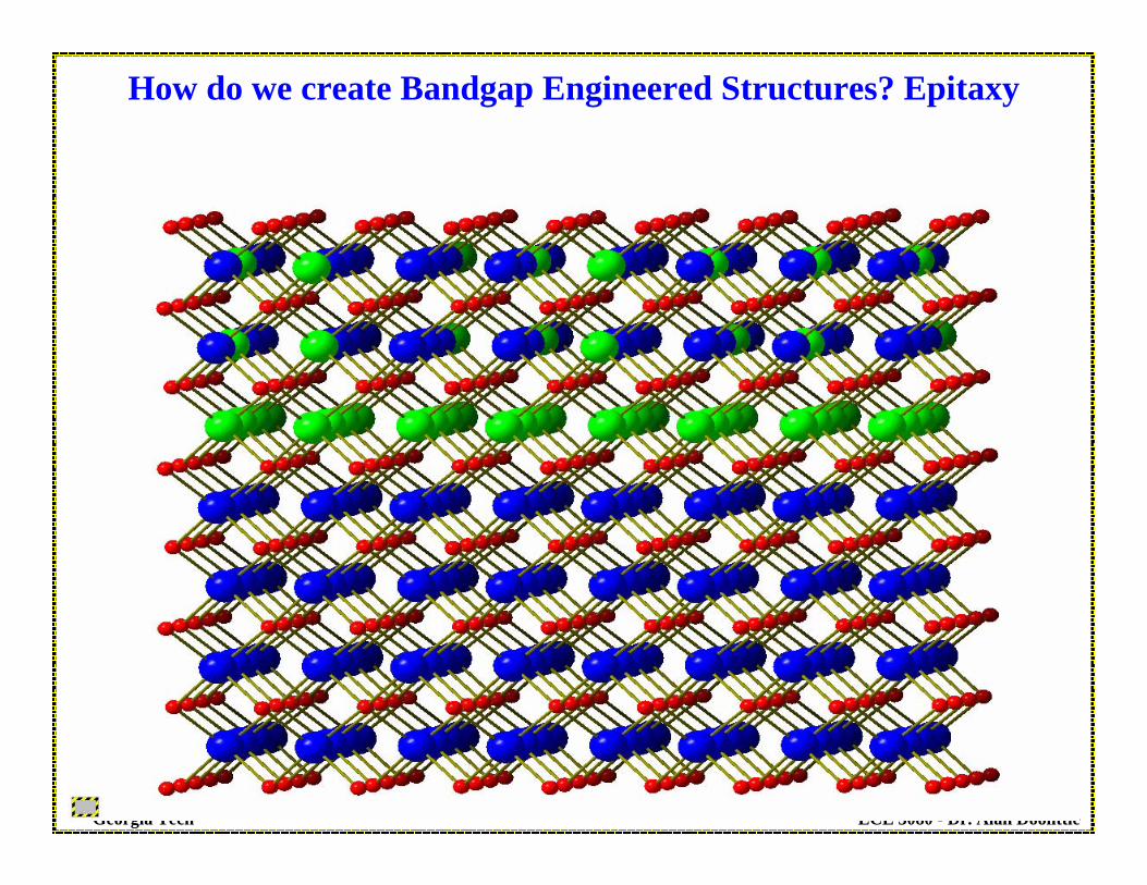
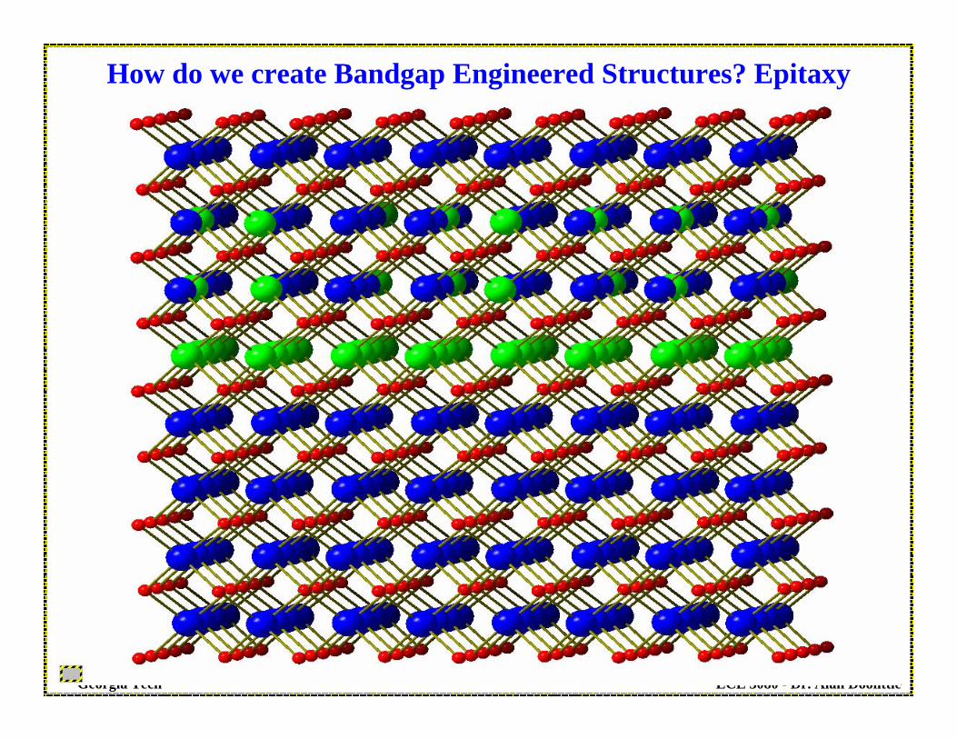
How do we create Bandgap Engineered Structures? Epitaxy
•Repeating a crystalline structure by the atom by atom addition.
•Chemistry controls the epitaxy to insure that, for example, Ga bonds only to N and not Ga-Ga or N-N bonds*.
*A small number of “antisite” defects (Ga-Ga or N-N bonds) actually do form but are typically in the parts per trillion concentration.
ECE 3080 - Dr. Alan DoolittleGeorgia Tech
How do we create Bandgap Engineered Structures? Epitaxy
ECE 3080 - Dr. Alan DoolittleGeorgia Tech
How do we create Bandgap Engineered Structures? Epitaxy
ECE 3080 - Dr. Alan DoolittleGeorgia Tech
How do we create Bandgap Engineered Structures? Epitaxy

ECE 3080 - Dr. Alan DoolittleGeorgia Tech
How do we create Bandgap Engineered Structures? Epitaxy

ECE 3080 - Dr. Alan DoolittleGeorgia Tech
How do we create Bandgap Engineered Structures? Epitaxy
ECE 3080 - Dr. Alan DoolittleGeorgia Tech
How do we create Bandgap Engineered Structures? Epitaxy
ECE 3080 - Dr. Alan DoolittleGeorgia Tech
How do we create Bandgap Engineered Structures? Epitaxy

ECE 3080 - Dr. Alan DoolittleGeorgia Tech
How do we create Bandgap Engineered Structures? Epitaxy
ECE 3080 - Dr. Alan DoolittleGeorgia Tech
How do we create Bandgap Engineered Structures? Epitaxy

ECE 3080 - Dr. Alan DoolittleGeorgia Tech
How do we create Bandgap Engineered Structures? Epitaxy
ECE 3080 - Dr. Alan DoolittleGeorgia Tech
How do we create Bandgap Engineered Structures? Epitaxy

ECE 3080 - Dr. Alan DoolittleGeorgia Tech
How do we create Bandgap Engineered Structures? Epitaxy
GaN
GaN
GaN
GaN
AlN
AlGaN
AlGaN
GaN
Ec Ev

ECE 3080 - Dr. Alan DoolittleGeorgia Tech
Effusion Furnaces
Partially disassembled MBE system for clarity
RHEED Gun
Gas Source (oxygen)
Shutter mechanism
MBE
ECE 3080 - Dr. Alan DoolittleGeorgia Tech
Commercial Veeco® MBE
ECE 3080 - Dr. Alan DoolittleGeorgia Tech
Primarily used for II-VI, and III-V semiconductors, special metallic oxides and metals.
Metal Organic Chemical Vapor Deposition (MOCVD)•Many materials that we wish to deposit have very low vapor pressures and thus are difficult to transport via gases.•One solution is to chemically attach the metal (Ga, Al, Cu, etc…) to an organic compound that has a very high vapor pressure. Organic compounds often have very high vapor pressure (for example, alcohol has a strong odor).•The organic-metal bond is very weak and can be broken via thermal means on wafer, depositing the metal with the high vapor pressure organic being pumped away.•Care must be taken to insure little of the organic byproducts are incorporated. Carbon contamination and unintentional Hydrogen incorporation are sometimes a problem.
Human Hazard: As the human body absorbs organic compounds very easily, the metal organics are very easily absorbed by humans. Once in the body, the weak metal-organic bond is easily broken, thus, poisoning the body with heavy metals that often can not be easily removed by normal bodily functions. In extreme cases, blood transfusion is the only solution (if caught in time). “Luckily”, such poisoning is rare as the pyrophoric (flammable in air) nature of most metal organic means the “victim” is burned severely before he/she can be contaminated.
Alternative Methods: MOCVD

ECE 3080 - Dr. Alan DoolittleGeorgia Tech
Commercial Thomas Swan® MOCVD
ECE 3080 - Dr. Alan DoolittleGeorgia Tech
Ec
Ev
E=-qVArbitrary Reference Energy
Kinetic Energy
Potential Energy
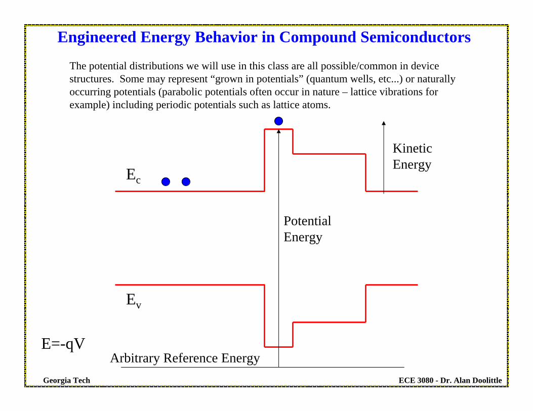
Engineered Energy Behavior in Compound Semiconductors
The potential distributions we will use in this class are all possible/common in device structures. Some may represent “grown in potentials” (quantum wells, etc...) or naturally occurring potentials (parabolic potentials often occur in nature – lattice vibrations for example) including periodic potentials such as lattice atoms.

ECE 3080 - Dr. Alan DoolittleGeorgia Tech
So much for the introduction. Now on to the
meat of the course.