Lec. 27+28: Weather Forecasting & Analysis (Ch 13 + Appendix)
Upload
udai-singhCategory
view
216download
0description

Analog & Digital ElectronicsCourse No: PH-218
Lec-26: Metal Oxide Field Effect Transistors
(MOSFETs)
Department of Physics,
Indian Institute of Technology Guwahati, India 1
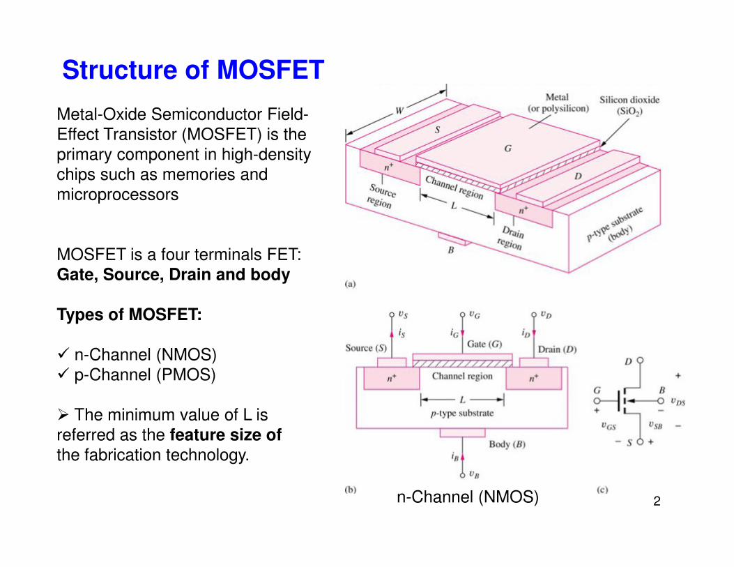
Structure of MOSFET
Metal-Oxide Semiconductor Field-
Effect Transistor (MOSFET) is the
primary component in high-density
chips such as memories and
microprocessors
MOSFET is a four terminals FET:
Gate, Source, Drain and body
Types of MOSFET:
� n-Channel (NMOS)
� p-Channel (PMOS)
� The minimum value of L is
referred as the feature size ofthe fabrication technology.
n-Channel (NMOS) 2

Operation of n channel MOSFET
Body and source are tied to ground.
When VDS= 0 and VGS=0, source-body
and drain-body diode are off hence no
current can flow & MOSFET is in cutoff.
When VDS= 0 and 0 < VGS < Vt ,Vertical
electric field established. Holes repelled electric field established. Holes repelled
and depletion region under gate oxide
forms.
When VDS= 0 and VGS > Vt, A n type
inversion layer formed underneath the
gate oxide when VGS reaches a critical
value Vt, called threshold voltage. The
channel connects source to drain and
current flow between them. 3

Operation of n channel MOSFET� When VGS > Vt and a small VDS is applied
– Current flows from D to S (Electrons flow from S to D) and IDS ∝ VDS
Electric field in the oxide is highest at the source end of channel. Thus many electrons are injected near the source.
Electric field in the oxide is lowest at the drain end of channel. Thus few electrons are induced near the drain.
� Increasing VGS above Vt increases the electron density in the channel, and in
turn increases the conductivity between D & S, hence IDS increases.
� MOSFET behave like a voltage controlled resistor.
4

Operation of n channel MOSFET� Increase VDS Decrease VGD less electrons at the drain side of the channel
� When VDS ≥ VGS – Vt then VGD ≤ Vt so no channel exists at the drain side. The
channel “pinches-off”
� When channel pinches off, electrons still flows from S to D
� Electrons are diffused from the channel to the depletion region near D, where they
are drifted by the lateral E-field to the D
� Further increase of VDS - no effect on the channel - current is “saturated” and the � Further increase of VDS - no effect on the channel - current is “saturated” and the
transistor is in “Saturation Mode”
5

I-V Characteristics of n channel MOSFET� MOS structure looks like a parallel plate capacitor and VGC is composed of two
components: Vt to form the channel and (VGC-Vt) to accumulate negative charges in
the channel.
CVQchannel = LWCt
LWC ox
ox
ox==
ε)
2(
tDSGS
tGCV
VVVVV −
−=−=
L
VEv DS
nn µµ ==
Charge is carried by electrons and
Carrier velocity v is proportional to the
lateral E-field between S and D.DSnV
L
v
Lt
µ
2
==L lateral E-field between S and D.DSnVv µ
6

I-V Characteristics of n channel MOSFET
In the Linear region, drain current depends on
– How much charge is in the channel
– How fast the charge is moving
t
QI channel
= ]2
1)[(
2
DSDStGSoxn VVVV
L
WCI −−=
µ
For V > V and V ≥ V = V – V : I is independent of VFor VGS > Vt and VDS ≥ Vdsat = VGS – Vt : ID is independent of VDS
In Saturation mode
7

Depletion and Enhancement mode MOSFET� A depletion-type MOSFET has a built-in channel by fabrication i.e. It is ON
when no gate-source voltage is applied and need to apply a negative VGS to
turn off device. Vt is negative for NMOS.
� MOSFET is said to be enhancement type if gate-source voltage is applied
to turn on the transistor. Vt is positive for NMOS.
8

Channel length Modulation
9
The effective channel length L
is reduced by ∆L and hence IDS
increases.

P-channel MOSFET (PMOS)
10

Complimentary MOSFET (CMOS)
Complementary MOS or CMOS integrated-circuit technologies provide
both NMOS and PMOS on a same IC
11

Supplement slide: How inversion layer forms?
12
p-Si
Reference: E.F. Schubert, Renesselaer Polytechic Institute 2003

(2) When VG < 0 (Accumulation): Gate bias is –ve so Ef at the gate goes up. Since M and S have much higher
conductivity than O so voltage between Gate and channel mostly drops at oxide. An
Electric field will be generated at oxide.
Supplement slide: Accumulation (VG < 0)
13Reference: E.F. Schubert, Renesselaer Polytechic Institute 2003

Supplement slide: Accumulation (VG < 0)
14
Reference: E.F. Schubert, Renesselaer Polytechic Institute 2003

Supplement slide: Depletion (VG > 0)
15
Reference: E.F. Schubert, Renesselaer Polytechic Institute 2003
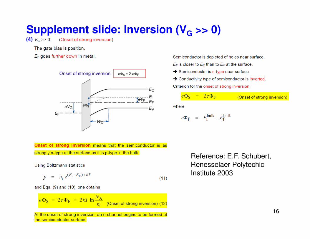
Supplement slide: Inversion (VG >> 0)
16
Reference: E.F. Schubert,
Renesselaer Polytechic
Institute 2003