Leakage Current Optimization and Layout Migration for 90 ...xqi/cktDevMag_paper_print.pdf · S...
9
S ubthreshold leakage currents consume a significant fraction of total circuit power in 90- and 65-nm technologies. Generation of library cells for low-leakage current is important for achieving low-power application- specific integrated circuit (ASIC) designs. Since a typical ASIC library may contain thousands of cells, efficient techniques are required. In this article, a complete automated leakage optimization flow is presented. It includes an efficient circuit optimization engine to optimize device channel length and width while keeping cell delay increase and cell area change minimal. Optimization results show about 30% leakage current reduction with only several percent active area and dynamic power increase. The optimization flow starts with SPICE net lists, including parasitic resistance- capacitance (RC) extracted from the existing library. After leakage optimization, revised cell layouts are generated and characterized based on the optimized net lists. In addition, investigations indicate that the optimization process has little impact on cell noise margins and that new cell layout variations Xiaoning Qi, Sam C. Lo, Alex Gyure, Yansheng Luo, Mahmoud Shahram, Kishore Singhal, and Don B. MacMillen Leakage Current Optimization and Layout Migration for 90- and 65-nm ASIC Libraries ©MASTER SERIES 39 ■ IEEE CIRCUITS & DEVICES MAGAZINE ■ SEPTEMBER/OCTOBER 2006 8755-3996/06/$20.00 ©2006 IEEE
Transcript of Leakage Current Optimization and Layout Migration for 90 ...xqi/cktDevMag_paper_print.pdf · S...

Subthreshold leakage currents consume a significantfraction of total circuit power in 90- and 65-nmtechnologies. Generation of library cells for low-leakagecurrent is important for achieving low-power application-
specific integrated circuit (ASIC) designs. Since a typical ASIClibrary may contain thousands of cells, efficient techniques arerequired. In this article, a complete automated leakageoptimization flow is presented. It includes an efficient circuitoptimization engine to optimize device channel length andwidth while keeping cell delay increase and cell areachange minimal. Optimization results show about 30%leakage current reduction with only several percentactive area and dynamic power increase. Theoptimization flow starts with SPICE netlists, including parasitic resistance-capacitance (RC) extracted from theexisting library. After leakageoptimization, revised cell layouts aregenerated and characterized basedon the optimized net lists. Inaddition, investigations indicatethat the optimization process haslittle impact on cell noise marginsand that new cell layout variations
Xiaoning Qi, Sam C. Lo,Alex Gyure, Yansheng Luo,
Mahmoud Shahram, Kishore Singhal, and
Don B. MacMillen
Leakage Current Optimization and Layout Migration for 90- and 65-nm ASIC Libraries
©MASTER SERIES
39 ■IEEE CIRCUITS & DEVICES MAGAZINE ■ SEPTEMBER/OCTOBER 2006 8755-3996/06/$20.00 ©2006 IEEE

■ 40 IEEE CIRCUITS & DEVICES MAGAZINE ■ SEPTEMBER/OCTOBER 2006
from placement, routing, and compaction have little effect onthe results. This efficient automated layout to layout cellleakage optimization flow is most suitable for leakagereduction and library migration for 90- and 65-nm ASICdesigns and beyond.
Due to aggressive process technology scaling, it is now pos-sible to integrate several billions of transistors onto a singledie. Smaller feature sizes make transistor density higher, andreduction in oxide thickness enables faster transistors. Toachieve low active power in designs, circuit supply voltage andcorresponding transistor threshold voltage must be scaleddown. Unfortunately, the reduction in threshold voltage hasalso resulted in an increase in channel leakage currents thatcan increase total power consumption substantially. Physical
gate lengths will continue to scale down to 8 nm by 2017, aspredicted by the 2005 International Technology Roadmap forSemiconductors (ITRS’05) [1], notwithstanding technicalchallenges such as leakage currents and process variations.Figure 1 plots subthreshold leakage current for different tech-nologies, which shows that the subthreshold leakage (Ioff)
increases exponentially as process technologies scale, includ-ing the projected leakage at the 45-nm technology node. Toensure that designs can benefit from higher density and per-formance in nanometer technologies, leakage optimizationand design-for-manufacturing (DFM) have become essentialelements of nanometer library design.
Leakage mechanisms include subthreshold leakage, gateoxide tunneling leakage, junction leakage, hot-carrier injec-tion leakage, gate-induced drain leakage, and punch-throughleakage currents [2]. In Figure 2, some of these leakage com-ponents are illustrated. At the 180-nm technology node, sub-threshold leakage currents emerge as an issue. At the 90-nmtechnology node, subthreshold leakage and gate leakagebecome a problem. At even smaller gate lengths, all leakagecomponents will be evident. However, studies find that sub-threshold leakage current is the dominant mechanism in 90-and 65-nm technologies. Subthreshold current, also known asweak inversion conduction current, between source and drainin a MOS transistor occurs when the gate voltage is below thetransistor threshold voltage (Vth). Although threshold voltageis decreasing with technology scaling, the subthreshold slope,a measure of transistor switch-off characteristics or transi-tions between weak and strong inversion regions are mainlycontrolled by material properties which have not improveddrastically with scaling.
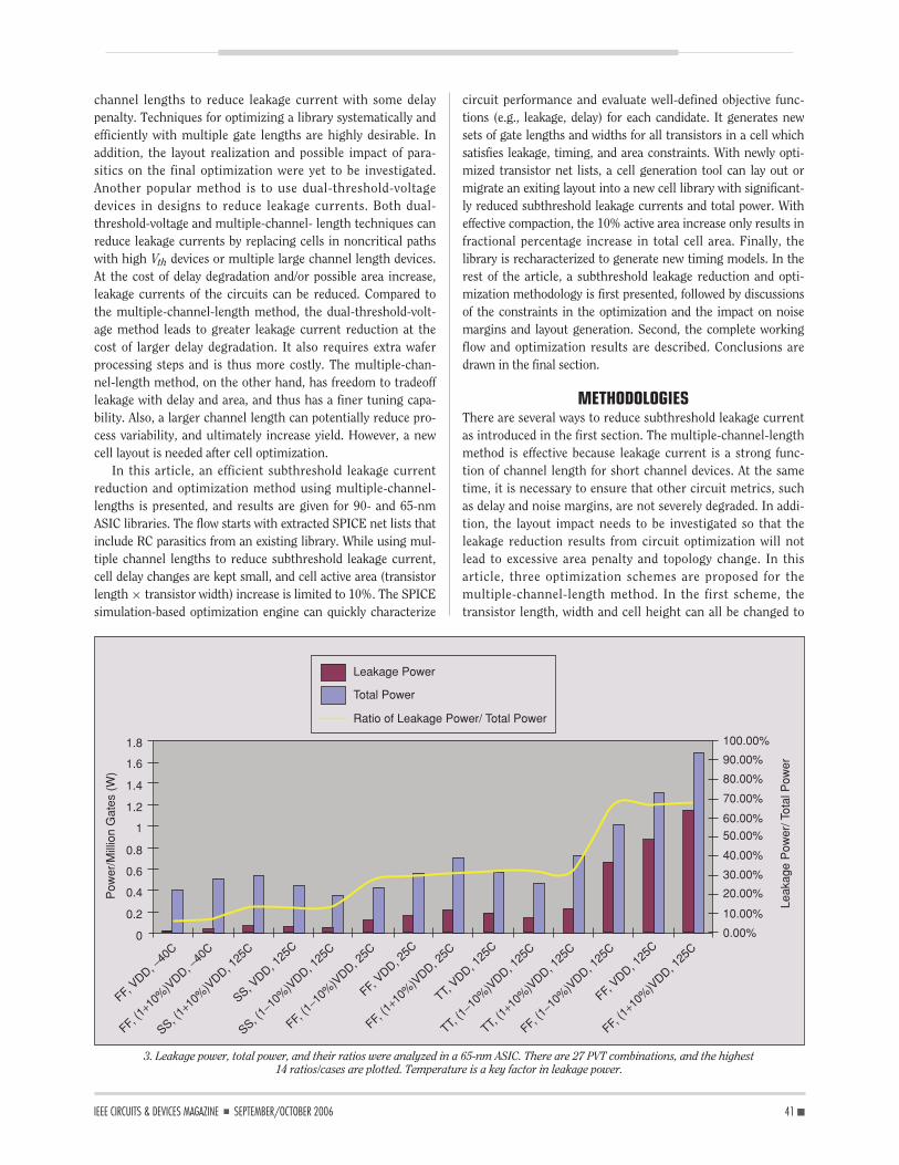
Circuit simulations reveal that in the 65-nm technology,subthreshold leakage power can be as high as 60% of totalchip power as shown in Figure 3, where several process cor-ner, supply voltage, and temperature (PVT) combinations weresimulated for an 800-MHz high-end ASIC. In the simulation,assumptions were made that 95% of gates were quiet, and 5%of gates were switching [3]. It is evident that temperature, aswell as process corners and supply voltage, has significantimpact on leakage currents. As an increasing number ofdesigns move into the 90- and 65-nm technologies, it isimportant to reduce subthreshold leakage current in creatingASIC cell libraries or to migrate an existing library to a low-leakage library to minimize total chip power.
Several techniques have been proposed to reduce sub-threshold leakage currents [2], [4]. These include device andprocess optimization [5] and circuit design techniques toreduce and control subthreshold leakage [6], [7]. More specifi-cally, the techniques involve supply voltage optimization [8],reverse body biasing [9], and multiple-threshold voltage assign-ment and state assignment [10], [11]. Moreover, Yuan proposeda gate replacement method [12] that required leakage-opti-mized gate libraries. Lichtensteiger [13] discussed leakagemodeling to estimate leakage currents in ASIC libraries, butleakage reduction and optimization techniques were not pro-posed. Sirisantana [14] proposed the use of multiple large
1. Sub-threshold leakage currents increase exponentiallywith technologies [2]. Our simulations were based on
third-party foundry technologies.
10,000
1,000
100
10
1
Temperature = 80°C
Intel Data (IEDM'04)Our Simulation250 nm
180 nm
130 nm
90 nm
65 nm45 nm
Technologies
I off
(nA
/m
)
2. Leakage currents include source drain sub-threshold leakagecurrent and gate leakage current. In 90- and 65-nm technologies,
subthreshold leakage current dominates.
Gate Oxide TunnelingLeakage
N+ N+
Punch-Through Leakage
Gate-Induced Drain Leakage
Subthreshold LeakageCurrent
Reverse BiasCurrent
41 ■IEEE CIRCUITS & DEVICES MAGAZINE ■ SEPTEMBER/OCTOBER 2006
channel lengths to reduce leakage current with some delaypenalty. Techniques for optimizing a library systematically andefficiently with multiple gate lengths are highly desirable. Inaddition, the layout realization and possible impact of para-sitics on the final optimization were yet to be investigated.Another popular method is to use dual-threshold-voltagedevices in designs to reduce leakage currents. Both dual-threshold-voltage and multiple-channel- length techniques canreduce leakage currents by replacing cells in noncritical pathswith high Vth devices or multiple large channel length devices.At the cost of delay degradation and/or possible area increase,leakage currents of the circuits can be reduced. Compared tothe multiple-channel-length method, the dual-threshold-volt-age method leads to greater leakage current reduction at thecost of larger delay degradation. It also requires extra waferprocessing steps and is thus more costly. The multiple-chan-nel-length method, on the other hand, has freedom to tradeoffleakage with delay and area, and thus has a finer tuning capa-bility. Also, a larger channel length can potentially reduce pro-cess variability, and ultimately increase yield. However, a newcell layout is needed after cell optimization.
In this article, an efficient subthreshold leakage currentreduction and optimization method using multiple-channel-lengths is presented, and results are given for 90- and 65-nmASIC libraries. The flow starts with extracted SPICE net lists thatinclude RC parasitics from an existing library. While using mul-tiple channel lengths to reduce subthreshold leakage current,cell delay changes are kept small, and cell active area (transistorlength × transistor width) increase is limited to 10%. The SPICEsimulation-based optimization engine can quickly characterize
circuit performance and evaluate well-defined objective func-tions (e.g., leakage, delay) for each candidate. It generates newsets of gate lengths and widths for all transistors in a cell whichsatisfies leakage, timing, and area constraints. With newly opti-mized transistor net lists, a cell generation tool can lay out ormigrate an exiting layout into a new cell library with significant-ly reduced subthreshold leakage currents and total power. Witheffective compaction, the 10% active area increase only results infractional percentage increase in total cell area. Finally, thelibrary is recharacterized to generate new timing models. In therest of the article, a subthreshold leakage reduction and opti-mization methodology is first presented, followed by discussionsof the constraints in the optimization and the impact on noisemargins and layout generation. Second, the complete workingflow and optimization results are described. Conclusions aredrawn in the final section.
METHODOLOGIESThere are several ways to reduce subthreshold leakage currentas introduced in the first section. The multiple-channel-lengthmethod is effective because leakage current is a strong func-tion of channel length for short channel devices. At the sametime, it is necessary to ensure that other circuit metrics, suchas delay and noise margins, are not severely degraded. In addi-tion, the layout impact needs to be investigated so that theleakage reduction results from circuit optimization will notlead to excessive area penalty and topology change. In thisarticle, three optimization schemes are proposed for themultiple-channel-length method. In the first scheme, thetransistor length, width and cell height can all be changed to
3. Leakage power, total power, and their ratios were analyzed in a 65-nm ASIC. There are 27 PVT combinations, and the highest14 ratios/cases are plotted. Temperature is a key factor in leakage power.
1.8
1.6
1.4
1.2
1
0.8
0.6
0.4
0.2
0
Pow
er/M
illio
n G
ates
(W
)
100.00%
90.00%
80.00%
70.00%
60.00%
50.00%
40.00%
30.00%
20.00%
10.00%
0.00%
FF, VDD, −
40C
FF, (1
+10%
)VDD, −
40C
SS, (1+1
0%)V
DD, 125
C
SS, VDD, 1
25C
SS, (1−1
0%)V
DD, 125
C
FF, (1
−10%
)VDD, 2
5C
FF, VDD, 2
5C
FF, (1
+10%
)VDD, 2
5C
TT, VDD, 1
25C
TT, (1
−10%
)VDD, 1
25C
TT, (1
+10%
)VDD, 1
25C
FF, (1
−10%
)VDD, 1
25C
FF, VDD, 1
25C
FF, (1
+10%
)VDD, 1
25C
Leak
age
Pow
er/ T
otal
Pow
er
Leakage Power
Total Power
Ratio of Leakage Power/ Total Power
■ 42 IEEE CIRCUITS & DEVICES MAGAZINE ■ SEPTEMBER/OCTOBER 2006
reduce leakage current while maintaining the circuit delay.This is suitable for generating a new cell library where there isflexibility in cell height. The second scheme is to change tran-sistor length and width, but not the cell height, which leads tomoderate delay degradation and area increase. The thirdscheme is to increase transistor length, but not transistorwidth or the cell height. This scheme leads to minimal cellarea increase with relatively larger delay degradation. Both thesecond and third schemes are suitable for migrating an exitinglibrary to a new low-leakage library. While the transistorlength and width optimization techniques apply to all threeschemes, this article will focus on the second and thirdschemes in terms of layout generation.
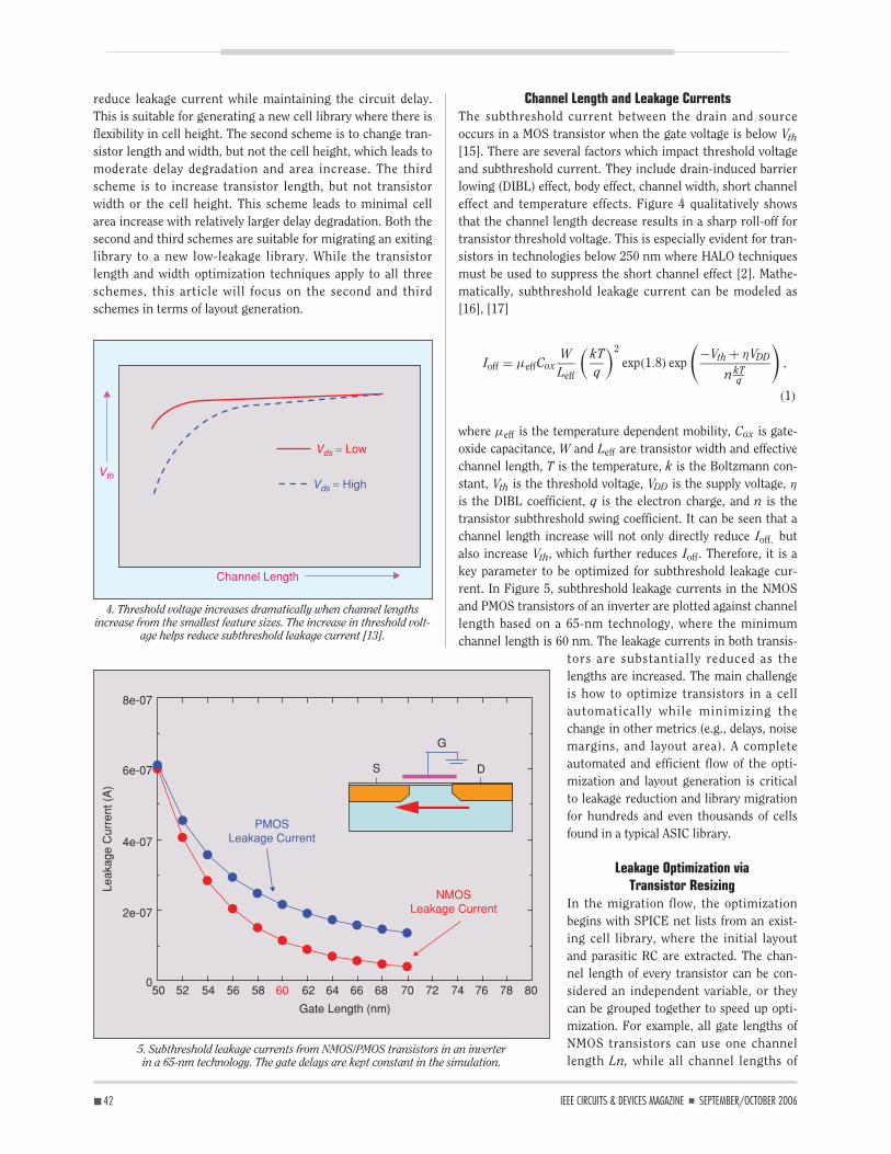
Channel Length and Leakage CurrentsThe subthreshold current between the drain and sourceoccurs in a MOS transistor when the gate voltage is below Vth
[15]. There are several factors which impact threshold voltageand subthreshold current. They include drain-induced barrierlowing (DIBL) effect, body effect, channel width, short channeleffect and temperature effects. Figure 4 qualitatively showsthat the channel length decrease results in a sharp roll-off fortransistor threshold voltage. This is especially evident for tran-sistors in technologies below 250 nm where HALO techniquesmust be used to suppress the short channel effect [2]. Mathe-matically, subthreshold leakage current can be modeled as[16], [17]
Ioff = µeffCoxWLeff
(kTq
)2
exp(1.8) exp
(−Vth + ηVDD
n kTq
),
(1)
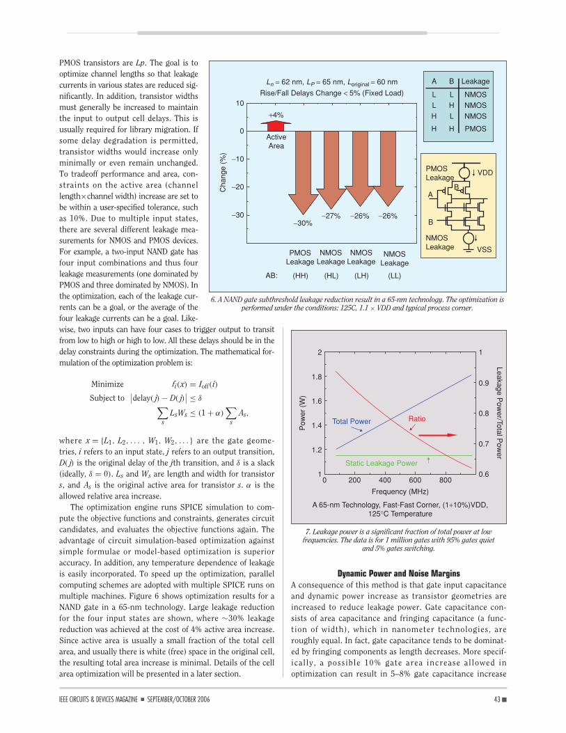
where µeff is the temperature dependent mobility, Cox is gate-oxide capacitance, W and Leff are transistor width and effectivechannel length, T is the temperature, k is the Boltzmann con-stant, Vth is the threshold voltage, VDD is the supply voltage, ηis the DIBL coefficient, q is the electron charge, and n is thetransistor subthreshold swing coefficient. It can be seen that achannel length increase will not only directly reduce Ioff, butalso increase Vth, which further reduces Ioff. Therefore, it is akey parameter to be optimized for subthreshold leakage cur-rent. In Figure 5, subthreshold leakage currents in the NMOSand PMOS transistors of an inverter are plotted against channellength based on a 65-nm technology, where the minimumchannel length is 60 nm. The leakage currents in both transis-
tors are substantially reduced as thelengths are increased. The main challengeis how to optimize transistors in a cellautomatically while minimizing thechange in other metrics (e.g., delays, noisemargins, and layout area). A completeautomated and efficient flow of the opti-mization and layout generation is criticalto leakage reduction and library migrationfor hundreds and even thousands of cellsfound in a typical ASIC library.
Leakage Optimization viaTransistor Resizing
In the migration flow, the optimizationbegins with SPICE net lists from an exist-ing cell library, where the initial layoutand parasitic RC are extracted. The chan-nel length of every transistor can be con-sidered an independent variable, or theycan be grouped together to speed up opti-mization. For example, all gate lengths ofNMOS transistors can use one channellength Ln, while all channel lengths of
5. Subthreshold leakage currents from NMOS/PMOS transistors in an inverterin a 65-nm technology. The gate delays are kept constant in the simulation.
PMOSLeakage Current
NMOSLeakage Current
8e-07
6e-07
4e-07
2e-07
050 52 54 56 58 60 62 64 66 68 70 72 74 76 78 80
Gate Length (nm)
Leak
age
Cur
rent
(A
)
S
G
D
4. Threshold voltage increases dramatically when channel lengthsincrease from the smallest feature sizes. The increase in threshold volt-
age helps reduce subthreshold leakage current [13].
Vds = Low
Vds = HighVth
Channel Length
43 ■IEEE CIRCUITS & DEVICES MAGAZINE ■ SEPTEMBER/OCTOBER 2006
PMOS transistors are Lp. The goal is tooptimize channel lengths so that leakagecurrents in various states are reduced sig-nificantly. In addition, transistor widthsmust generally be increased to maintainthe input to output cell delays. This isusually required for library migration. Ifsome delay degradation is permitted,transistor widths would increase onlyminimally or even remain unchanged.To tradeoff performance and area, con-straints on the active area (channellength×channel width) increase are set tobe within a user-specified tolerance, suchas 10%. Due to multiple input states,there are several different leakage mea-surements for NMOS and PMOS devices.For example, a two-input NAND gate hasfour input combinations and thus fourleakage measurements (one dominated byPMOS and three dominated by NMOS). Inthe optimization, each of the leakage cur-rents can be a goal, or the average of thefour leakage currents can be a goal. Like-wise, two inputs can have four cases to trigger output to transitfrom low to high or high to low. All these delays should be in thedelay constraints during the optimization. The mathematical for-mulation of the optimization problem is:
Minimize fi(x) = Ioff(i)
Subject to∣∣delay( j) − D( j)
∣∣ ≤ δ∑
sLsWs ≤ (1 + α)
∑
sAs,
where x = {L1, L2, . . . , W1, W2, . . . } are the gate geome-tries, i refers to an input state, j refers to an output transition,D( j) is the original delay of the jth transition, and δ is a slack(ideally, δ = 0). Ls and Ws are length and width for transistors, and As is the original active area for transistor s. α is theallowed relative area increase.
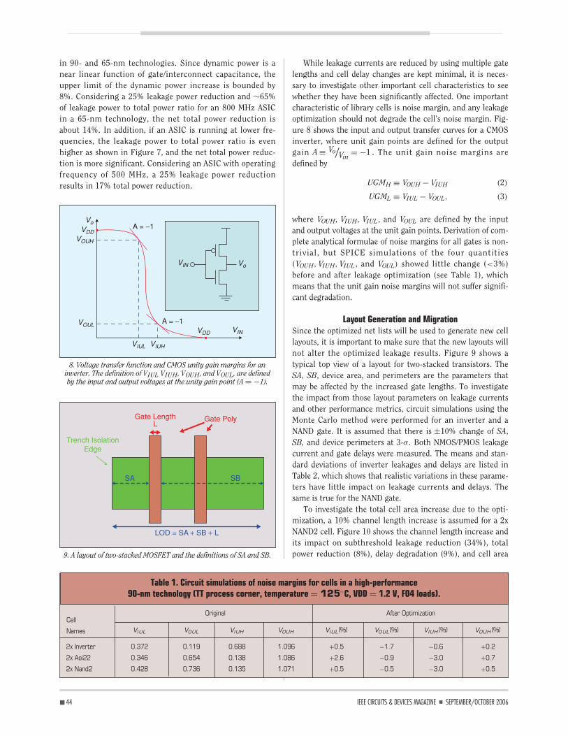
The optimization engine runs SPICE simulation to com-pute the objective functions and constraints, generates circuitcandidates, and evaluates the objective functions again. Theadvantage of circuit simulation-based optimization againstsimple formulae or model-based optimization is superioraccuracy. In addition, any temperature dependence of leakageis easily incorporated. To speed up the optimization, parallelcomputing schemes are adopted with multiple SPICE runs onmultiple machines. Figure 6 shows optimization results for aNAND gate in a 65-nm technology. Large leakage reductionfor the four input states are shown, where ∼30% leakagereduction was achieved at the cost of 4% active area increase.Since active area is usually a small fraction of the total cellarea, and usually there is white (free) space in the original cell,the resulting total area increase is minimal. Details of the cellarea optimization will be presented in a later section.
Dynamic Power and Noise MarginsA consequence of this method is that gate input capacitanceand dynamic power increase as transistor geometries areincreased to reduce leakage power. Gate capacitance con-sists of area capacitance and fringing capacitance (a func-tion of width), which in nanometer technologies, areroughly equal. In fact, gate capacitance tends to be dominat-ed by fringing components as length decreases. More specif-ically, a possible 10% gate area increase allowed inoptimization can result in 5–8% gate capacitance increase
6. A NAND gate subthreshold leakage reduction result in a 65-nm technology. The optimization isperformed under the conditions: 125C, 1.1 × VDD and typical process corner.
+4%
0
10
−10
−30
−20
−30%−27% −26% −26%
PMOSLeakage
NMOSLeakage
NMOSLeakage
NMOSLeakage
AB:
Cha
nge
(%)
ActiveArea
Ln = 62 nm, LP = 65 nm, Loriginal = 60 nm
Rise/Fall Delays Change < 5% (Fixed Load)
A B Leakage
L L
L
L
H
H
H H
NMOS
NMOS
NMOS
PMOS
PMOSLeakage
NMOSLeakage
VDD
B
B
A
VSS
(HH) (HL) (LH) (LL)
7. Leakage power is a significant fraction of total power at lowfrequencies. The data is for 1 million gates with 95% gates quiet
and 5% gates switching.
Total Power Ratio
Static Leakage Power
0 200 400 600 800
Frequency (MHz)
1
1.2
1.4
1.6
1.8
2
Pow
er (
W)
0.6
0.7
0.8
0.9
1
A 65-nm Technology, Fast-Fast Corner, (1+10%)VDD,125°C Temperature
Leakage Pow
er/Total Pow
er
■ 44 IEEE CIRCUITS & DEVICES MAGAZINE ■ SEPTEMBER/OCTOBER 2006
in 90- and 65-nm technologies. Since dynamic power is anear linear function of gate/interconnect capacitance, theupper limit of the dynamic power increase is bounded by8%. Considering a 25% leakage power reduction and ∼65%of leakage power to total power ratio for an 800 MHz ASICin a 65-nm technology, the net total power reduction isabout 14%. In addition, if an ASIC is running at lower fre-quencies, the leakage power to total power ratio is evenhigher as shown in Figure 7, and the net total power reduc-tion is more significant. Considering an ASIC with operatingfrequency of 500 MHz, a 25% leakage power reductionresults in 17% total power reduction.
While leakage currents are reduced by using multiple gatelengths and cell delay changes are kept minimal, it is neces-sary to investigate other important cell characteristics to seewhether they have been significantly affected. One importantcharacteristic of library cells is noise margin, and any leakageoptimization should not degrade the cell’s noise margin. Fig-ure 8 shows the input and output transfer curves for a CMOSinverter, where unit gain points are defined for the outputgain A ≡ Vo
/Vin
= −1 . The unit gain noise margins aredefined by
UGMH ≡ VOUH − VIUH (2)
UGML ≡ VIUL − VOUL, (3)
where VOUH, VIUH, VIUL , and VOUL are defined by the inputand output voltages at the unit gain points. Derivation of com-plete analytical formulae of noise margins for all gates is non-trivial, but SPICE simulations of the four quantities(VOUH, VIUH, VIUL , and VOUL) showed little change (<3%)before and after leakage optimization (see Table 1), whichmeans that the unit gain noise margins will not suffer signifi-cant degradation.
Layout Generation and MigrationSince the optimized net lists will be used to generate new celllayouts, it is important to make sure that the new layouts willnot alter the optimized leakage results. Figure 9 shows a typical top view of a layout for two-stacked transistors. The SA, SB, device area, and perimeters are the parameters thatmay be affected by the increased gate lengths. To investigatethe impact from those layout parameters on leakage currentsand other performance metrics, circuit simulations using theMonte Carlo method were performed for an inverter and aNAND gate. It is assumed that there is ±10% change of SA,SB, and device perimeters at 3-σ . Both NMOS/PMOS leakagecurrent and gate delays were measured. The means and stan-dard deviations of inverter leakages and delays are listed inTable 2, which shows that realistic variations in these parame-ters have little impact on leakage currents and delays. Thesame is true for the NAND gate.
To investigate the total cell area increase due to the opti-mization, a 10% channel length increase is assumed for a 2xNAND2 cell. Figure 10 shows the channel length increase andits impact on subthreshold leakage reduction (34%), totalpower reduction (8%), delay degradation (9%), and cell area
8. Voltage transfer function and CMOS unity gain margins for aninverter. The definition of VIUL VIUH, VOUH, and VOUL, are definedby the input and output voltages at the unity gain point (A = −1).
Vo
VoVDD
VOUH
VOUL
VIUL VIUH
VIN
VDD VIN
A = −1
A = −1
9. A layout of two-stacked MOSFET and the definitions of SA and SB.
SA SB
Trench IsolationEdge
Gate LengthL
Gate Poly
LOD = SA + SB + L
Original After Optimization
VIUL VOUL VIUH VOUH VIUL(%) VOUL(%) VIUH (%) VOUH (%)
2x Inverter 0.372 0.119 0.688 1.096 +0.5 −1.7 −0.6 +0.2
2x Aoi22 0.346 0.654 0.138 1.086 +2.6 −0.9 −3.0 +0.7
2x Nand2 0.428 0.736 0.135 1.071 +0.5 −0.5 −3.0 +0.5
Table 1. Circuit simulations of noise margins for cells in a high-performance90-nm technology (TT process corner, temperature = 125◦C, VDD = 1.2 V, FO4 loads).
Cell
Names

45 ■IEEE CIRCUITS & DEVICES MAGAZINE ■ SEPTEMBER/OCTOBER 2006
change (0%). The new layout generated from Synopsys librarylayout tool CADABRA is shown side by side with the originalcell layout in Figure 11. It is worthwhile noting thatCADABRA has the ability to maintain the important featuresof the source layout, and it can also increase the number ofvias for DFM purposes. The layout migration takes the origi-nal layout as a source layout and maintains the same place-ment and routing topology as far as possible except forincreasing channel lengths. Recompaction is then applied togenerate a new optimized layout for the low-leakage library.Since standard cell widths are in increments of layoutcolumns/grids, quite often the layout optimized cell does notgrow in size unless there is very little white space in the orig-inal layout. Results for more complexcells will be given in the next section.
TOOLS AND RESULTSBased on the methodology describedin the previous section, a leakageoptimized library characterizationflow was developed. This automaticflow consists of several commercialtools: 1) a SPICE simulator, 2) a stan-dard cell library characterization tool,3) a circuit optimizer, 4) a library lay-out generation and migration tool,and 5) a parasitic extraction tool. Thisflow has been applied to an estab-lished commercial library in a 90-nmtechnology. Results show that theflow works efficiently and achievessignificant subthreshold leakagepower reduction.
Optimization FlowThree sets of data are required for the flow: 1) a subset of theLiberty timing library, 2) the GDSII cell layouts, and 3)
Leakage and Delay Mean σ
NMOS Leakage 243.1 nA 1.7 nA
PMOS Leakage 524.2 nA 454.9 pA
Output-Rise Delay 26.2 ps 47.3 fs
Output-Fall Delay 30.4 ps 46.3 fs
Table 2. Monte Carlo simulation of layout impact on aninverter: Leakage currents and delay in a 90-nm technology.
10. A NAND 2x2 cell. Device channel lengths are increased by 10% from 100 nm in a 90-nmtechnology. Simulation is performed under TT process corner, VDD = 1.0 v, and temperature of 125°C.
VDD
PMOSLeakage
NMOSLeakage
VSS
BA
B
Gate Length Changefrom 0.1 µm – 0.11 µm
LeakageCurrent
TotalPower
AverageDelay
CellArea
−34%
−8% 0%
9%
−40
−30
−20
−10
0
10
Cha
nge
Ver
sus
Nom
inal
Cas
e (%
)
11. Migration of NAND 2x2 layout after subthreshold leakage current optimization. There is no cell area increase in the newlayout while channel lengths are increased by 10%.
2.52
µm
2.52
µm
0.1 µm
1.12 µm
0.11 µm
1.12 µm
Source Layout New Layout

■ 46 IEEE CIRCUITS & DEVICES MAGAZINE ■ SEPTEMBER/OCTOBER 2006
postlayout standard cell SPICE net lists. The first step passesthe input files to a standard cell library characterization tool.The tool extracts information from the timing library such as
cell name, input and output pins, timing arc sensitization,loading capacitances, and input slews. The characterizationtool generates SPICE decks with appropriate arc sensitizationand different combinations of input states for each standardcell. Capacitance load and input slew are selected based onthe most commonly expected load and slope values. Measure-ments of leakage current, delay, and active area are generat-ed, which act as constraints for the second step of the flow.The second step is circuit optimization. The circuit optimizeruses the SPICE input decks and performs circuit simulationand optimization. The optimizer changes the channel lengthand width for every transistor in the standard cell. The finalstep is layout and library generation and characterization.During optimization, constraints can be set, for example:
✦ total active area increase is less than 10%✦ channel length increase is less than 10%✦ channel width is within the range of +/− 20%✦ delay change is within +/− 5%✦ target average leakage reduction of 25%.
To make this flow more practical, additional settings are required:✦ optimization step size for widths and lengths should be
on minimum layout grid increment✦ grouping multiple widths or
lengths together based on circuittopology and layout.
Ideally, the channel lengths of every tran-sistor would be an optimization variable.For large standard cells such as AOI, thismay result in a large number of optimiza-tion variables. A more efficient method isto group several widths or lengths intomacrovariables. The reduction in thenumber of free variables yields fasteroptimization run times and reduces lay-out complexity. The circuit optimizerperforms simulations using a commercialHSPICE simulator. Based on the mea-surement of area, delay, and leakage
Original After Optimization
Cell Names Active Area (fm2) Ioff (nA) �Active Area (%) �Ioff (%)
2x Inverter 140 337 10.29 −25.92
4x Buffer 390 1124 7.6 −27.6
1x Delay 265 457 6.04 −25.9
1x Mux2 427 650 4.33 −25.39
2x Xnor2 567 1267 6.24 −32.89
2x Aoi22 560 473 12.06 −26.68
2x Nand2 280 394 9.96 −26.45
6x Nand2 832 1770 7.61 −25.42
Average 432.63 809 8.02 −27.03
Table 3. Circuit optimization results based on a 90-nm CMOShigh performance library.
12. A complete flow of ASIC library optimization for leakage currents.
65- or 90-nm Library
Test Bench Creation
Circuit Optimization
Layout Optimization
Parasitic Extraction
Library Characterization
Optimized Library
DR, DRC, ERC GDSII
Leakage Total Power Delay New Cell Width Cell Width Change Migration Run Time
Cell Name Reduction (%) Reduction (%) Increase (%) (Columns) (1 Column = 0.28 mm) (h:min:sec)
2x Inverter 36 9 9 3 0 0:00:12
4x Buffer 37 11 13 6 0 0:00:28
1x Delay 33 14 11 8 −1 0:00:26
1x Mux2 33 17 13 10 1 0:00:55
2x Xnor2 35 17 11 11 0 0:00:50
2x Aoi22 33 8 11 7 0 0:00:43
2x Nand2 34 8 9 4 0 0:00:16
6x Nand2 35 12 9 11 1 0:00:39
4x D Flip-Flop 35 12 15 29 1 0:12:43
4x Scan Enable D 34 15 15 55 3 0:57:17
Flip-Flop
AVERAGES 35% 12% 12% 00:07:33
Table 4. Circuit optimization and layout migration results for a 90-nm technology CMOS library.

47 ■IEEE CIRCUITS & DEVICES MAGAZINE ■ SEPTEMBER/OCTOBER 2006
current, the circuit optimizer modifies the input variables andthen resimulates. This loop repeats until the optimization tar-gets are met. If the targets cannot be met, the optimizationterminates after a prespecified run time is reached. Once newtransistor sizes are obtained, the new library generation/migra-tion is completed by layout generation and library characteri-zation (see Figure 12).
Circuit Optimization and Layout Migration ResultsThis flow was tested on a production ASIC library in a 90-nmtechnology at 1.2 V supply and 125◦C. Eight representativecombinatorial standard cells were chosen for testing. Theselected cells cover most unique types of standard cells. Asshown in Table 3, an average of 27% subthreshold leakagereduction is achieved at an average 8% active area increase. Inthe table, “Active Area” is the active channel area, and Ioff isthe cell leakage current. The delay degradation is less than 1%.These techniques are also applicable to sequential cells. If moredelay degradation is permitted, one can choose to increasechannel lengths only and maintain the same transistor widths.This can significantly speed up the optimization process. Table4 shows the results of 10% channel length increase for all tran-sistors in eight combinatorial cells and two sequential cells in adifferent library. The average leakage reduction is ∼35% at theaverage cost of 12% delay degradation. The average layoutmigration time is about 7 min on a 3 GHz Intel Xeon Machine.
CONCLUSIONSLeakage current is of great concern for designs in nanometertechnologies. In 90- and 65-nm technologies, subthresholdleakage current dominates total leakage current. For a typicalASIC circuit running at several hundred megahertz frequen-cies, the subthreshold leakage power can be as high as 60% oftotal power. An important method for minimizing power inASIC libraries is reducing leakage current. In this article, acomplete automated leakage optimization flow that changeschannel lengths and widths with cell delay and active areaconstraints was discussed. Optimization results show thatthere is ∼30% leakage current reduction with a few percentactive area and delay increase. There is increase in dynamicpower, but the net total power reduction is significant. A uni-form increase of 10% in gate length results in ∼35% leakagereduction at the cost of ∼12% delay degradation. The total cellarea changes are minimal in both cases. The optimization flowbegins with SPICE net lists from an existing library, optimizesleakage currents subject to performance metrics and activearea increase constraints, and finishes with new layout genera-tion and characterization. Investigations indicate that theleakage optimization has little impact on cell noise marginand layout parasitic modifications do not affect optimizationresults. The efficient automatic layout-to-layout cell leakageoptimization flow is most suitable for leakage minimizationand library migration for 90- and 65-nm ASIC libraries.Future work includes applying the flow to situations wherelayout-dependent DFM and process variation objective func-tions are also optimized.
REFERENCES[1] “2005 international technology roadmap for semiconductor” [Online].
Available: http://public.itrs.net/
[2] K. Roy, S. Mukhopadhyay, and H. Mahmoodi-Meimand, “Leakage cur-rent mechanisms and leakage reduction techniques in deep-submi-crometer CMOS circuits,” Proc. IEEE, vol. 91, no. 2, pp. 305–327, Feb.2003.
[3] A. Chandrakasan, I. Yang, C. Vieri, and D. Antoniads, “Design consider-ations and tools for low-voltage digital system design,” in Proc. DesignAutomation Conf., June 1996, pp. 728–733.
[4] R. Brodersen, M. Horowitz, D. Markovic, B. Nikolic, and V. Stojanovic,“Methods for true power minimization,” in Proc. IEEE Int. Conf. Com-puter-Aided Design, San Jose, CA, 2002, pp. 35–42.
[5] S. Mukhopadhyay, A. Raychowdhury, and K. Roy, “Accurate estimationof total leakage in nanometer-scale bulk CMOS circuits based on devicegeometry and doping profile,” IEEE Trans. Computer-Aided Design, vol.24, no. 3, pp. 363–381, Mar. 2005.
[6] S. Borkar, “Circuit techniques for sub-threshold leakage avoidance,control, and tolerance,” in Proc. IEEE Electron Devices Meeting, SanFrancisco, Dec. 2004, pp. 421–424.
[7] K. Zhang, U. Bhattacharya, Z. Chen, F. Hamzaoglu, D. Murray, N.Vallepalli, Y. Wang, B. Zhang, and M. Bohr, “SRAM design on 65-nmCMOS technology with dynamic sleep transistor for leakage reduction,”IEEE J. Solid-State Circuits, vol. 40, no. 4, pp. 895–901, Apr. 2005.
[8] M. Mui, K. Banerjee, and A. Mehrotra, “Supply and power optimizationin leakage-dominant technologies,” IEEE Trans. Computer- AidedDesign, vol. 24, no. 9, pp. 1362–1371, Sept. 2005.
[9] N. Jayakumar, S. Dhar, and S. Khatri, “A self-adjusting scheme to deter-mine the optimum RBB by monitoring leakage currents,” in Proc.Design Automation Conf., Anaheim, CA, June 2005, pp. 43–46.
[10] F. Gao and J. Hayes, “Total power reduction in CMOS circuits via gatesizing and multiple threshold voltages,” in Proc. Design AutomationConf., Anaheim, CA, June 2005, pp. 31–36.
[11] D. Lee, D. Blaauw, and D. Sylvester, “Static leakage reduction throughsimultaneous Vt/Vox and state assignment,” IEEE Trans. Computer-Aided Design, vol. 24, no. 7, pp. 1014–1029, July 2005.
[12] L. Yuan and G. Qu, “Enhanced leakage reduction technique by gatereplacement,” Proc. Design Automation Conf., Anaheim, CA, June 2005,pp. 47–50.
[13] S. Lichtensteiger, L. Wissel, J. Engel, and P. Sulva, “Modeling leakagein ASIC libraries,” IEEE Custom Integrated Circuits Conf., San Jose, CA,Sept. 2005, pp. 609–612.
[14] N. Sirisantana, L. Wei, and K. Roy, “High-performance low-powerCMOS circuits using multiple channel length and multiple oxide thick-ness,” in Proc. IEEE Int. Conf. Computer Design: VLSI Computers Pro-cessors, 2000, pp. 227–232.
[15] Y. Taur and T.H. Ning, Fundamentals of Modern VLSI Devices. Cam-bridge, U.K.: Cambridge Univ. Press, 1998, ch. 2, pp. 94–95.
[16] B.J. Sheu, D.L. Scharfetter, P.K. Ko, and M.C. Jeng, “BSIM: Berkeleyshort-channel IGFET model for MOS transistors,” IEEE J. Solid-StateCircuits, vol. 22, no. 4, pp. 558–566, Aug. 1987.
[17] B. Chatterjee, M. Sachdev, S. Hsu, R. Krishnamurthy, and S. Borkar,“Effectiveness and scaling trends of leakage control techniques for sub-100 nm CMOS technologies,” in Proc. Int. Symp. Low-PowerElectronics, Seoul, Korea, 2003, pp. 122–127.
Xiaoning Qi , Sam C. Lo , Alex Gyure , Yansheng Luo ,Mahmoud Shahram, Kishore Singhal, and Don B. MacMillenare with Synopsys, Inc, Mountain View, California. E-mail:[email protected].