LEAD-FREE SOLDERING PROCESSES IN THE ELECTRONIC … · lead-free solders in the soldering processes...
15
Lead-Free Soldering Implementation Rolim do Carmo et al. Ciência e Tecnologia dos Materiais, Vol. 19, n.º 3/4, 2007 15 2ª MENÇÃO HONROSA (OE) – DIA MUNDIAL DOS MATERIAIS 2007 LEAD-FREE SOLDERING PROCESSES IN THE ELECTRONIC INDUSTRY – INDUSTRIAL IMPLEMENTATION AT SMES ROLIM DO CARMO 1 , MARGARIDA PINTO 1 , ROGÉRIO COLAÇO 2 , DAG ANDERSSON 3 1 Instituto de Soldadura e Qualidade ([email protected] ; [email protected]) 2 Instituto Superior Técnico ([email protected]) 3 IVF - Industrial Research and Development Corporation ([email protected]) ABSTRACT: Following the implementation of the new European environmental directives, Restriction of the Use of Certain Hazardous Substances (RoHS) and Waste Electrical and Electronic Equipment (WEEE), which involve the ban of lead from electronic and electrical products, this work presents process development work, production and reliability testing of real products from several electric and electronic assemblers using lead-free commercial solders that have been tested and monitored to ensure the reliability of the final products. The results were compared with the ones using tin/lead solders, in terms of performance and reliability of the joints obtained. This work aims to help the implementation of the lead-free solders in the soldering processes and supply the SMEs more information about real products and conditions that might be compared with theirs. The reliability tests and characterisation of the real products from several companies showed that the lead-free boards demonstrated a good performance under testing, being equivalent or better than the tin/lead ones. The defects or anomalies found in most of the joints (voiding and pad lifting) result from the manufacturing process. Most of the defects were found in through-hole devices and were due to component failures and not from the joint integrity. The degradation after the reliability tests of both types of solders is similar. The SMEs are engaged in taking this opportunity to reach a higher quality performance level in their processes. Some of the companies embraced this “forced” transition to upgrade and improve their process and facilities, bringing better capabilities and opportunities to their businesses. The objective of this work aims to be a tool of information to the SMEs of the electrical and electronic sector, in order to help them in the transition to lead-free soldering. Keywords: Lead-free solder, Soldering, Electronics, Reliability, PCB, RoHS. RESUMO: No decorrer da implementação das recentes directivas ambientais Europeias: Restrição do Uso de Substâncias Perigosas (RUSP) e Resíduos de Equipamentos Eléctricos e Electrónicos (REEE) surge a proibição do uso de chumbo em produtos eléctricos e electrónicos. Este trabalho apresenta o estudo de desenvolvimento de processo, produção e testes de fiabilidade em produtos reais de diversas empresas do sector eléctrico e electrónico. Vários tipos de soldas comerciais foram usadas e testadas de modo a permitir a comparação em termos de performance das soldas sem chumbo face às com chumbo. O presente trabalho tem como objectivo o apoio às PMEs (Pequenas e Médias Empresas) durante a implementação da soldadura sem chumbo nos seus processos industriais e fornecer-lhes mais informação sobre produtos reais que lhes permita comparar com a sua própria produção. Os testes de fiabilidade e a caracterização feita nos produtos em estudo demonstraram que as placas soldadas sem chumbo possuem uma boa performance em teste e são equivalentes ou superiores às placas soldadas com soldas com chumbo. Os defeitos e anomalias encontradas nas juntas soldadas resultam, essencialmente, do processo de fabrico e não das pastas e soldas utilizadas. Na sua maioria, as falhas encontradas nas placas são devidas a falha de componentes e não da integridade das juntas. A degradação das soldas após teste é similar nos dois tipos de solda. As PMEs estão motivadas em aproveitar esta transição “forçada” para melhorar as suas capacidades, equipamentos, processo e oportunidades de negócio. O objectivo final deste trabalho é fornecer informação às PMEs do sector eléctrico e electrónico, de modo a apoiar a sua transição para a soldadura sem chumbo. Palavras chave: Solda sem chumbo, Soldadura, Electrónica, Fiabilidade, PCB, RUSP.
Transcript of LEAD-FREE SOLDERING PROCESSES IN THE ELECTRONIC … · lead-free solders in the soldering processes...

Lead-Free Soldering Implementation Rolim do Carmo et al.
Ciência e Tecnologia dos Materiais, Vol. 19, n.º 3/4, 2007 15
2ª MENÇÃO HONROSA (OE) – DIA MUNDIAL DOS MATERIAIS 2007
LEAD-FREE SOLDERING PROCESSES IN THE ELECTRONIC INDUSTRY – INDUSTRIAL
IMPLEMENTATION AT SMES
ROLIM DO CARMO1, MARGARIDA PINTO
1, ROGÉRIO COLAÇO
2, DAG ANDERSSON
3
1 Instituto de Soldadura e Qualidade ([email protected]; [email protected])
2 Instituto Superior Técnico ([email protected])
3 IVF - Industrial Research and Development Corporation ([email protected])
ABSTRACT: Following the implementation of the new European environmental directives, Restriction of the Use of
Certain Hazardous Substances (RoHS) and Waste Electrical and Electronic Equipment (WEEE), which involve the ban of
lead from electronic and electrical products, this work presents process development work, production and reliability
testing of real products from several electric and electronic assemblers using lead-free commercial solders that have been
tested and monitored to ensure the reliability of the final products. The results were compared with the ones using tin/lead
solders, in terms of performance and reliability of the joints obtained. This work aims to help the implementation of the
lead-free solders in the soldering processes and supply the SMEs more information about real products and conditions that
might be compared with theirs.
The reliability tests and characterisation of the real products from several companies showed that the lead-free boards
demonstrated a good performance under testing, being equivalent or better than the tin/lead ones. The defects or anomalies
found in most of the joints (voiding and pad lifting) result from the manufacturing process. Most of the defects were found
in through-hole devices and were due to component failures and not from the joint integrity. The degradation after the
reliability tests of both types of solders is similar.
The SMEs are engaged in taking this opportunity to reach a higher quality performance level in their processes. Some of
the companies embraced this “forced” transition to upgrade and improve their process and facilities, bringing better
capabilities and opportunities to their businesses.
The objective of this work aims to be a tool of information to the SMEs of the electrical and electronic sector, in order to
help them in the transition to lead-free soldering.
Keywords: Lead-free solder, Soldering, Electronics, Reliability, PCB, RoHS.
RESUMO: No decorrer da implementação das recentes directivas ambientais Europeias: Restrição do Uso de Substâncias
Perigosas (RUSP) e Resíduos de Equipamentos Eléctricos e Electrónicos (REEE) surge a proibição do uso de chumbo em
produtos eléctricos e electrónicos. Este trabalho apresenta o estudo de desenvolvimento de processo, produção e testes de
fiabilidade em produtos reais de diversas empresas do sector eléctrico e electrónico. Vários tipos de soldas comerciais
foram usadas e testadas de modo a permitir a comparação em termos de performance das soldas sem chumbo face às com
chumbo. O presente trabalho tem como objectivo o apoio às PMEs (Pequenas e Médias Empresas) durante a
implementação da soldadura sem chumbo nos seus processos industriais e fornecer-lhes mais informação sobre produtos
reais que lhes permita comparar com a sua própria produção.
Os testes de fiabilidade e a caracterização feita nos produtos em estudo demonstraram que as placas soldadas sem chumbo
possuem uma boa performance em teste e são equivalentes ou superiores às placas soldadas com soldas com chumbo. Os
defeitos e anomalias encontradas nas juntas soldadas resultam, essencialmente, do processo de fabrico e não das pastas e
soldas utilizadas. Na sua maioria, as falhas encontradas nas placas são devidas a falha de componentes e não da
integridade das juntas. A degradação das soldas após teste é similar nos dois tipos de solda.
As PMEs estão motivadas em aproveitar esta transição “forçada” para melhorar as suas capacidades, equipamentos,
processo e oportunidades de negócio.
O objectivo final deste trabalho é fornecer informação às PMEs do sector eléctrico e electrónico, de modo a apoiar a sua
transição para a soldadura sem chumbo.
Palavras chave: Solda sem chumbo, Soldadura, Electrónica, Fiabilidade, PCB, RUSP.

Rolim do Carmo et al. Lead-Free Soldering Implementation
16 Ciência e Tecnologia dos Materiais, Vol. 19, n.º 3/4, 2007
1. Introduction
1.1 Objectives
This work results from the implementation of the new
European environmental directives, particularly the
Restriction of the Use of Certain Hazardous Substances
(RoHS). From all the restrictions imposed by the Restriction
of the Use of Certain Hazardous Substances (RoHS) and
Waste Electrical and Electronic Equipment (WEEE)
directives, banning of lead from electronic and electrical
products had one of the biggest impacts on this industrial
sector (see sub-chapters 2.1.1 and 2.1.2). Small and Medium
Enterprises (SME) that have to strive with the huge
competitiveness of the market are now facing a new
obstacle, the substitution of solder alloys and all the
consequences that this change implies.
This work presents process development work, production
and reliability testing of real products from several partners
with commercial solders that have been tested and
monitored to ensure the required reliability of the new lead-
free solders and compare them with the previous lead
containing ones. It aims to help the implementation of the
lead-free solders in the soldering processes and supply to the
SMEs more information about real products and conditions
that might be compared with theirs, and not only results
obtained from ideal conditions as in the laboratory. Finally
the objective of this work is to be a tool of information to
the SMEs of the electrical and electronic sector, in order to
help them in the transition to lead-free soldering.
1.2 Workplan
The present work is based in an industrial research project
and compiles in a brief manner several of the main results
obtained with electric and electronic industrial assemblers
from Portugal, Spain and United Kingdom. The first part of
this work brings an analysis of the European directives and
their impact in industry, and some information about the
basic principles of soldering in electronics. A description of
the work carried out and results are presented in the second
part. Finally the economical and environmental impacts are
evaluated, and the discussion and conclusions of the work is
presented. Several industrial products were selected from
each of the industrial partners for the work presented in the
second part of this thesis. These products were
manufactured and all data recorded, including the level of
the defects found for each type of solder tested. The boards
were visually inspected before and after the reliability and
functionality tested. Some joints from each board were then
selected and characterised by optical and electronic
microscopy.
2. Electronic industry issues related to European directives
2.1 European directives
2.1.1 RoHS
The Restriction of the Use of Certain Hazardous Substances
in Electrical and Electronic Equipment – RoHS Directive –
implements the provisions of the European Parliament and
Council under the Directive 2002/95/EC. The RoHS
Directive bans the introduction on the EU market of new
Electrical and Electronic Equipment (EEE) containing more
than the permitted levels of lead, cadmium, mercury,
hexavalent chromium and both polybrominated biphenyl
(PBB) and polybrominated diphenyl ether (PBDE) flame
retardants from 1st July 2006. Manufacturers will need to
ensure that their products - components and sub-assemblies
of such products - comply with the requirements of the
RoHS Directive. [1, 2]
2.1.2 WEEE
The Waste Electrical and Electronic Equipment Directive
(WEEE Directive) is the European Community Directive
2002/96/EC on waste electrical and electronic equipment.
The purpose of this directive is the prevention of WEEE,
and in addition, to regulate/stimulate the reuse, recycling
and other forms of recovery of such wastes so as to reduce
the disposal of waste [3]. The directive imposes the
responsibility for the disposal of WEEE on the
manufacturers of such equipment. Those companies should
establish an infrastructure for collecting WEEE, in such a
way that "Users of electrical and electronic equipment from
private households should have the possibility of returning
WEEE at least free of charge". Also, the companies are
compelled to use the collected waste in an ecological-
friendly manner, either by ecological disposal or by
reuse/refurbishment of the collected WEEE. [4, 5]
2.2 Lead-free industrial implementation concerns
The main issue that comes from the prohibition of lead alloy
solders is the increase of the melting point that is inherent to
the alternative solders. This increase of the melting point of
the solders has several important implications to the
manufacturing process. Surveys were carried out before the
implementation of the RoHS directive to the electric and
electronic industry participating in the project, in order to
investigate their concerns and possible problems. The results
showed that the main concerns were related to [6]:
• Investment in new equipment or upgrades;
• Thermal limitations of some components and materials;
• Thermal profile and temperatures to be used;
• Low cost reliable solders;
• Reliability of the products;
• Bath contamination on wave soldering;
• Solderability on rework process;
• Differences in the joint appearance that has a great
impact in inspection.
Some of these concerns have become a reality with the
transition to the lead-free process, others have been
overcome or even not found at all, e.g. decrease of the
products reliability under single standard tests. A lot of work
has been done in this area and a lot more still has to be done,
not only to achieve the implementation of the directives but
to take the electric and electronic sector to another level.

Lead-Free Soldering Implementation Rolim do Carmo et al.
Ciência e Tecnologia dos Materiais, Vol. 19, n.º 3/4, 2007 17
3. Soldering in electronics 3.1 Basic principles of soldering
Soldering is one of the oldest processes that use melting to
join two metals. It is defined to be all the joining processes
that do not melt the base material, the joint is produced by
heating and adding another metallic alloy, which melting
point is lower than the “solidus” temperature of the base
material. The alloy penetrates the joint, filling it, by
capillarity [7]. Efficient functioning of electrical and
electronic equipment is in many ways dependent on the
correct interconnection of electrical components. This
interconnection relies to the most part on soldering.
In electronics, Printed Circuit Boards (PCB) are commonly
used to mechanically support and electrically connect
electronic components using conductive copper paths
laminated onto a non conductive substrate. Some PCB’s are
composed of one up to more than twenty-four conductive
layers separated by other layers of insulating material
laminated together. The conductive layers are almost
invariably made of copper in all types of boards [8]. Layers
may be connected together through drilled holes (vias), to
form an electrical connection. These vias can be
electroplated or alternately small rivets can be inserted. In
every PCB small copper traces or tracks are visible on the
surface, these traces are made by adhering a layer of copper
over the entire substrate and then removing the unwanted
copper by etching, using a mask, leaving only the desired
copper traces. Pads to which components will be mounted
are normally plated, because bare copper oxidizes quickly,
reducing solderabillity. Platings like OSP (organic surface
preservative), Immersion silver and ENIG (electroless nickel
with immersion gold) are used [9].
3.1.1 Thermal aspects
In soldering one of the most important parameters is the
soldering temperature (Tsd). As regarding Tsd there is a
dilemma: the parts to be soldered should be heated to a
temperature high enough to be wetted by the solder but on
the other hand, the temperature that the components suffer
during the assembly process should not be so high that can
affect their operating characteristics. This issue has become
more problematic with the introduction of lead-free solders.
The components have to withstand temperatures higher than
217ºC (lead-free solder melting point), instead of 183ºC
(lead solder melting point) with the eutectic tin/lead solders.
Some components are not prepared for this process
changeover and cannot stand the higher temperature
demands (Fig. 1).
Figure 1 – Example of a capacitor that was not suited to
lead-free soldering temperatures [6].
Each component has its size, geometry, heat capacity and
other characteristics that should be kept in mind. To achieve
a good solderability over the whole board a well designed
temperature profile has to be used, especially with lead-free
and the consequent decrease of the process window. The
process window T changed from 40-45ºC to 10-15ºC
leaving almost no margin between the melting point and the
damaging point [8]. Lead-free solder have smaller process
windows because the temperatures of the reflow soldering
process are basically determined by the melting point of the
solder alloy. For adequate soldering, every point in the
board has to reach at least the melting point of the alloy.
This means that we have to deliver at least 20ºC higher than
the melting point for even distribution of temperatures. On
the other hand, components have a maximum temperature
that they can endure without damage. Thus, in the lead-free
solders with higher soldering temperature the gap to max
component temperature is decreased [6].
Pre-heating is very important in all lead-free soldering
processes in order to facilitate wetting, reduce contact time,
prevent thermal shock from room temperature to soldering
temperature and to activate the flux agent [8]. To avoid the
thermal differences in the board pre-heat should be use in all
processes (reflow, wave, selective soldering…).
Temperature profiling is essential in order to assure that the
peak temperatures of the components are not being
compromised. Using a set of thermocouples attached on the
boards can give valuable information about the temperatures
distribution among board, components and solder. This is an
excellent tool for setting up the process.
3.2 Fluxes
One of the primary purposes of fluxes is to prevent
oxidation in the base material (substrate). Solders can attach
very well to copper (Cu), but poorly if copper oxide is
present, which form quickly at high temperatures. Fluxes are
to a large extent inert at room temperature, but become
strongly reducing at high temperatures, mitigating the
formation of metal oxides. The second objective of fluxes is
to act as a wetting agent in the soldering process, increasing
the surface tension of the substrate and promote wettability.
And the third objective is to aid the heat transfer to the joint
area [8].
3.3 Solder Alloys
3.3.1 Alloys
Lead containing solders have been used extensively in
microelectronic applications to form electrical
interconnections between packaging levels, to facilitate heat
dissipation, to provide mechanical/physical support and to
serve as a solderable surface finish layer on PCB’s and lead
frames [10]. This wide use of lead containing solders is due
to the low melting point of the tin (Sn)/lead (Pb) alloy
(183ºC), good wettability, good mechanical and electrical
properties, and relative low cost.
As mentioned before, due to European restrictions lead has
been banned from solder alloys and a new era has begun.
The demand for new lead-free alloys was a priority concern

Rolim do Carmo et al. Lead-Free Soldering Implementation
18 Ciência e Tecnologia dos Materiais, Vol. 19, n.º 3/4, 2007
and several alloys were tested and are currently being
experimented. In the following table some examples of
solder alloys commercially used are presented:
Table 1 – Examples of commercial solder alloys
compositions and their melting points [6].
Solder Alloy Melting Point
(ºC)
63Sn/37Pb 183
60Sn/40Pb 183-187 Lead
62Sn/36Pb/2Ag 179
96.5Sn/3.5Ag 221
99.3Sn/0.7Cu 227
96.3Sn/3.2Ag/0.5Cu 217-218 Lead-free
96Sn/3.8Ag/0.7Cu 218
3.3.2 Metallurgy
Lead alloys
Alloys of this simple eutectic system are composed of
primary dendrites of either tin-rich or lead-rich solid
solution surrounded by eutectic. The eutectic occurs at
61.9% tin (183ºC) and consists of lead-rich and tin-rich
phases either lamellae or globules, depending on the
solidification rate. The higher the solidification rate the
greater the probability of formation of a globular eutectic.
These solders have relatively fast solid state reactions with
other elements such as copper, leading to the formation of
intermetallic compounds in the vicinity of the solder. The
molten eutectic tin/lead solder during solidification
separates into two different solids, a lead-rich phase and a
tin-rich phase.
Sn/Ag/Cu alloys
Tin/silver eutectic formation is very important for lead-free
solders in electronic industry. The eutectic composition for
this alloy is located at 96.5 wt% (Sn) and 3.5 wt% (Ag),
with a melting point of 221ºC. During solidification, when
the temperature reaches below the eutectic tie-line, the (Sn)
solid phase and intermediate phase form heterogeneously
together from the liquid (L).
)%2.73()%100()%5.96(º221 SnSnSnSnL C γβ +−⎯⎯ →⎯
(1)
As the (Sn) phase grows, the excess (Ag) atoms in the liquid
are rejected from the tips of the (Sn) phase, and will diffuse
laterally in a short distance to the phase (Ag3Sn). On the
other hand, the excess of (Sn) atoms rejected from the
phase will diffuse to the tips of the near (Sn) phase. The
(Sn) phase in the eutectic composition 96.5 Sn/3.5 Ag
predominates over the phase; the (Ag) solute is dissolved
in the (Sn) phase due to the longer distance to the phase.
The (Ag) enrichment in the liquid (the ones that do not
incorporate the phase) may cause constitutive super-
cooling and lead to the formation to dendrites, with phase
growing between the dendrite arms.
Another important eutectic formation for the solder alloys is
the tin/copper eutectic. This eutectic is located at 99.3 wt%
(Sn) and 0.7 wt% (Cu) with a melting point of 227ºC. As
previously discussed, this alloy also has a eutectic
transformation similar to the Sn/Ag eutectic.
)%9.60()%100()%99(º227 SnSnSnSnL C ηβ +−⎯⎯ →⎯
(2)
The corresponds to the Cu6Sn5 phase at 45.45 at% (Sn).
There are two possible binary eutectic reactions in the Sn-
rich region of the ternary system Sn/Ag/Cu. These reactions
are shown in the circle on the ternary phase diagram of
figure 2. Copper reacts with (Sn) to form a eutectic structure
of Sn-matrix phase and intermetallic compound phase
(Cu6Sn5) at 227ºC. A reaction between (Ag) and (Sn) forms
a eutectic structure of Sn-matrix phase and intermetallic
phase (Ag3Sn) at 221ºC. Finally, (Sn) solidifies in the end
leading to the ternary invariant eutectic point U7. (Ag) also
reacts with (Cu) to form a eutectic structure of Ag-rich
phase and Cu-rich phase at 779ºC. However, this
transformation is not detected in the solidification, is
thermodynamically favourable for (Ag) or (Cu) to react with
(Sn) to form the presented intermetallic compounds. The
ternary solder alloy Sn/Ag/Cu consists of a Sn-matrix phase,
intermetallic phase (Ag3Sn) and intermetallic compound
phase (Cu6Sn5) [11].
Figure 2 – Tin/silver/copper ternary phase diagram [12].
In terms of mechanical behaviour, in the Sn/Ag/Cu solders
the thermomechanical strains will concentrate near the pad
interfaces creating regions of high plastic deformation. In
these regions the (Sn) phase will recrystallise above room
temperature, producing fine grains that are more susceptible
to creep deformation (grain boundary sliding or cracking)
than the initial microstructure. Thus, providing an easy path
for crack propagation during thermo cycles and decreasing
the thermal fatigue life. In the Sn/Pb solders the fractures
appear on the same locations but due to the microstructural
coarsening of the (Sn) and (Pb) phases near the interface,
leading to a local softening and to fatigue crack propagation
[10].

Lead-Free Soldering Implementation Rolim do Carmo et al.
Ciência e Tecnologia dos Materiais, Vol. 19, n.º 3/4, 2007 19
3.3.3 Intermetallics
In the soldering process there are interfacial reactions
between two different materials. When the solder touches
the pad, two reactions take place at the interface solder/base
material (joint):
• Dissolution of the base material into the molten solder;
• Formation of an interfacial reaction product, consisting
of one or more elements from each of the solder and
base material compositions.
An intermetallic compound is one type of intermediate
phase that is a solid solution with intermediate ranges of
composition. Intermetallic compounds may form when two
metal elements have a limited mutual solubility. These
compounds possess new compositions of a certain
stoichiometric ratio of the two component elements for a
binary system. The new phases have different crystal
structures from those of their elemental components. The
properties of the resulting intermetallic compound generally
differ from those of the component metal, exhibiting fewer
metallic characteristics, such as reduced ductility, reduced
density and reduced conductivity [11].
The relatively hard Ag3Sn and Cu6Sn5 particles in the Sn-
matrix of Sn/Ag/Cu alloys can strengthen the alloy through
the building of long-range internal stress. These hard
particles can also serve as the most effective blocks for
fatigue crack propagation. The formation of these particles
can lead to finer grains, the finer the intermetallic particles
are, the finer the microstructure will be. This facilitates the
grain boundary gliding mechanisms leading to extended
fatigue lifetime under elevated temperatures. The thin
intermetallic layers provide the necessary permanent bond
with the substrate, acting as “fixation phase”. However, if
the intermetallic layers become thicker the mechanical
properties of the solder joint will weaken, due to the brittle
nature of the compounds and to the difference of the thermal
expansion between the intermetallics and the bulk solder.
This can lead to internal stress development, resulting in
crack formation along the solder/substrate interface.
Optimum thickness is expected to be in the range of 1 to 5
micron [11]. A nickel barrier can be applied over the copper
substrate to control the (Cu) dissolution and intermetallic
compound growth. This will lead to different reactions. If
the (Cu) pads are protected will an OSP coating, this one
will vaporize on reflow allowing the solder to touch the bare
(Cu) and form the intermetallics described above. When the
pads are protected with an ENIG (electroless
nickel/immersion gold) finish, the (Au) gold dissolves and
migrates into the solder promoting the intermetallic layer
formation between (Sn) and (Ni) – Ni3Sn4 or ternaries (Cu,
Ni)3Sn, (Cu, Ni)6Sn5. Literature presents the following
relationships [13]:
• Hardness (HV0.2: GPa) - (Cu, Ni)3Sn (5.5) > (Cu,
Ni)6Sn5 (4.9) > Cu6Sn5 (4.6) > Ni3Sn4 (4.3) > Ag3Sn
(1.4).
• Poisson ratio - Ag3Sn (0.35) > Cu6Sn5 (0.32) > (Cu,
Ni)6Sn5 (0.30) > (Cu, Ni)3Sn (0.27) > Ni3Sn4 (0.27).
• Young’s Modulus (GPa) - (Cu, Ni)3Sn (152) > (Cu,
Ni)6Sn5 (100)> Ni3Sn4 (58)> Cu6Sn5 (57)> Ag3Sn (55).
The Hardness and Young’s Modulus for the Sn/Ag/Cu
solder are 0.16 GPa and 50GPa, respectively. Ternary
intermetallic compounds like (Cu, Ni)3Sn and (Cu, Ni)6Sn5
are hard and brittle but appear only on second reflows and
are not usually observed. The Ag3Sn, Cu6Sn5 and Ni3Sn4
(with (Ni) barrier present) are more common. From the
relationships above, in comparison with the solder
properties these intermetallics present harder and more
brittle properties, which represent weaker zones in the
structure. Due to its elongated plate-like shape, the A3Sn
presents more damage in case of excess. This intermetallic
nucleates in front of the Cu6Sn5 layer and can grow rapidly
during cooling. The structural differences between the (Sn)
and Ag3Sn will induce a strain at the boundary between
them, leading to a preferential crack-propagation path,
especially when the Ag3Sn plates are aligned in the direction
of the crack propagation [14, 15].
3.4 Industrial soldering processes
There are at least two steps that a board must undergo before
the soldering stage: printing and component placement.
Soldering processes can be divided in the methods that
involve application of solder and heat simultaneously to the
parts to be soldered like wave soldering, and the reflow
method in which the solder and the heat are applied
separately. In the reflow method the heat can be local
(LASER, hot gas, hand soldering) or can be general (hot air
convection, infra-red radiation, a combination of both,
vapour phase) [8].
3.4.1 Reflow soldering
After the component placement on the pads (with the paste)
the boards will move in a conveyor to the reflow machine
(oven). The ovens produce heat by radiation through
ceramic infra-red heaters, it may also have fans to force
heated air to the assembly which is called infra-red
convention ovens. Normally, the reflow ovens are divided in
the following zones: pre-heat, soak, reflow and cooling,
following the same stages of a temperature profile. Reflow
ovens from 4 to 12 zones are available on the market.
3.4.2 Wave soldering
Wave soldering uses a pot with molten solder, the
components are placed on the PCB and pass through a wave
of solder, which is pumped from the pot. Wave soldering is
used for both through-hole and surface mount printed circuit
assemblies. For through-hole, the PCB touches the
“cascade” of molten solder and by capillarity the solder rises
through the holes and will form the joints. In the case of
SMDs, the components are placed with adhesives on the
PCB surface before being run through the molten solder
wave. A standard wave solder machine consists of three
zones: the fluxing zone, the pre-heating zone and the
soldering zone. An additional zone, cleaning, can be used
depending on the type of flux used [8].

Rolim do Carmo et al. Lead-Free Soldering Implementation
20 Ciência e Tecnologia dos Materiais, Vol. 19, n.º 3/4, 2007
3.5 Solder joints
3.5.1 Joint defects
Some of the examples that will be presented are not
considered as defects by IPC-610-D Standard, but for
simplifications purposes it shall be include this
“abnormalities” in the defect section. The IPC-A-610-D
standard presents acceptance requirements for the
manufacture of electronic assemblies. It is a manual that
includes detailed information, pictures and illustrations
portraying what is or not expected to encounter on an
electronic product [16]
The most common defects that can be found are described
bellow:
Solder shorts
The boards and components are getting smaller, and with
this also is the distance between components and
terminations. This effect appears mostly in wave processes
in which the solder does not separate from two or more
leads before the solder solidifies creating a short. Increasing
the flux quantity, optimise pre-heat, adjust process (speed)
can help to mitigate this problem [17].
Solder balls
Solder balls on the topside of the board after reflow
processes can be caused by the incompatibility between the
solder resist and solder paste. Solder resist affects the
mobility of the paste in the liquid state during reflow, as the
paste reflows and coalesces, some small parts of the solder
do not flow back to the joint (Fig. 3). It also can be due to
poor flux pre-heating [17].
Figure 3 – Solder balls defect. [16]
Voids
Most of the voids are caused by moisture that becomes
water vapour during the soldering process and expands,
sometimes voids can come out of solder while the solder is
in the liquid state, producing blow holes or non metallic
material that is trapped in the printed board and it is not
displaced during the soldering. Voids can be seen mostly on
the base of the board because the solder solidifies firstly on
the top and entraps them there. It reduces the joint strength
but it is not necessarily a reliability issue, if not in excess. A
good humidity storage control and baking the boards before
soldering can eliminate the moisture [17]. Figure 4 shows an
X-ray image of SOT23 (Small Outline Transistor) solder
joints after reflow on a lead free production line, where it
can be seen the voids in the solder.
Figure 4 – X-Ray image of a SOT23 presenting voiding on
all the joints [17].
Poor or incomplete filling
The hole is poorly filled or is not filled completely, the IPC
standard states that 75% of the hole must be filled (Fig. 5).
There are some possible reasons for this but the most
common are fluxing and heating issues [17].
Figure 5 – Example of poor wetting defect. [16]
3.5.2 Inspection and characterisation techniques
The inspection and characterisation can be made through
optical and/or electronic microscopy. The optical inspection
is done through an optical microscope following the
requisites of the standard IPC A-610-D class 3 and aims to
determine the quality of the joints with respect to visual
defects. The characterisation of solder joints implies the
preparation of the samples for inspection. That process
includes the micro-sectioning of the components, mounting
in resin, grinding and polishing. Only then the sample is
ready to be observed in the SEM (Scanning Electron
Microscope). This equipment allows seeing all the internal
and metallurgical defects present on the solder joint.
4. Lead-free process validation of commercial solders in industrial boards – Results overview
4.1 Introduction
In this chapter information is presented related with the
boards that were studied as well as all the results extracted
from the assembly process, visual inspection, reliability
tests, optical and electronic microscopy of the sectioned
samples. All the boards previously described were inspected
and tested.

Lead-Free Soldering Implementation Rolim do Carmo et al.
Ciência e Tecnologia dos Materiais, Vol. 19, n.º 3/4, 2007 21
4.2 Soldering of industrial boards
Information about the boards used in the present work is
briefly presented here:
Board A
This product, part of a video monitor unit, is a single sided
through-hole circuit board, with both leaded and surface
mount components. Surface mount components were placed
on the board using reflow cured adhesive and then soldered
along with the leaded components by wave soldering.
Table 2 – Summary of the board A soldering trials data.
Tin/Lead
Process Alloy Flux ProcessData Board
Wave 63Sn/37Pb
No clean,
rosin free
Alpha
Metals
E191/1
250°COSP
coated
Lead - Free
Wave SN100C
Sn/Cu/Ni
Water-
based, VOC
free, spray
DKL
Metals E-
Qual 355
flux
266°C
(two
waves)
OSP
coated
Board B
This product, part of an intercom system used in theatres, is
a single sided through-hole circuit board, with leaded
components only.
Table 3 – Summary of the board B soldering trials data.
Tin/Lead
Process Alloy Flux ProcessData Board
Hand 60Sn/40Pb
No-clean,
rosin free,
Interflux
IF14 fluxed
solder wire
350°C
(iron tip)
Sn/Pb
HASL
Lead - Free
Wave SN100C
Sn/Cu/Ni
Water-
based, VOC
free, spray
DKL Metals
E-Qual flux
255°C
(single
wave)
Lead-
free
HASL
Board C
This product is an assembly that is used in door lock
mechanisms in hotels. It has a reflow soldered, surface
mount circuit board, with surface mount devices only.
Table 4 – Summary of the board C soldering trials data.
Tin/Lead
Process Alloy Flux ProcessData Board
Reflow 62Sn/36Pb/2Ag
ROL0
no-clean
Koki
SE48-
M955
-Sn/Pb
HASL
Lead - Free
Reflow 96.5Sn/3.0Ag/0.5Cu
Koki
Eco Plus
S3X58-
M406
-Sn
finish
Board D
This product is used in telephone systems as part of a call
charging unit. The assembly has a double sided, plated
through-hole, mixed technology circuit board, with both
leaded and surface mount components on the top side only.
Surface mount components were reflow soldered to the
board, followed by wave soldering of the through-hole
components.
Table 5 – Summary of the board D soldering trials data.
Tin/Lead
Process Alloy Flux ProcessData Board
Reflow 62Sn/36Pb/2Ag
No-clean,
Alpha
Metals
UP78-T
-Au/Ni
plated
Wave 60Sn/40Pb
No-clean,
alcohol
based
flux;
Multicore
X33 12i
250°CAu/Ni
plated
Lead - Free
Reflow
95.5Sn/3.8Ag/0.7Cu
(4 boards)
96.5Sn/3.0Ag/0.5Cu
(4 boards)
95.5Sn/3.8Ag/0.7Cu
(8 boards)
Multicore
LF310
Alpha
metals
OM338
Multicore
LF318
-Au/Ni
plated
Wave SN100C
Sn/Cu/Ni
Hand–
sprayed,
no clean,
alcohol
based
flux;
Multicore
X33 12i
270ºCAu/Ni
plated
Board E
This product is part of a Taxicab display sign. It has a
double sided, plated through-hole circuit board, with both
leaded and surface mount components. The through-hole
components and surface mount chip resistors were
assembled by wave soldering, the connector was hand
soldered to the board.

Rolim do Carmo et al. Lead-Free Soldering Implementation
22 Ciência e Tecnologia dos Materiais, Vol. 19, n.º 3/4, 2007
Table 6 – Summary of the board E soldering trials data.
Tin/Lead
Process Alloy Flux ProcessData Board
Wave 63Sn/37Pb
No-clean,
rosin-free
foam
Kester
950E flux
250°CSn/Pb
HASL
Lead - Free
Wave 96.5Sn/3.0Ag/0.5Cu
No-clean,
rosin-free,
water
based
spray
Warton
Ecowave
45 flux
260°C
Lead-
free
HASL
Board F
This is a product used in digital display devices such as
LCD monitors to improve the image quality. The assembly
has a double sided, plated through-hole, mixed technology
circuit board, with both leaded and surface mount
components on the top side only. Surface mount
components were reflow soldered to the board, followed by
wave soldering of the through-hole components. The
tin/lead through-hole components were attached using the
lead-free process.
Table 7 – Summary of the board F soldering trials data.
Tin/Lead
Process Alloy Flux ProcessData Board
Reflow 63Sn/37Pb
No-clean,
ROL0,
Indium
Corporation
NC-SMQ-
92J
- ENIG
Lead - Free
Reflow 96.5Sn/3.0Ag/0.5Cu
No-clean,
Alpha
Metals
OM-338
- ENIG
Wave SACX
Sn/Ag/Cu/Bi
No-clean,
rosin based,
sprayed
Alpha
Metals EF-
6000 flux
260ºC ENIG
4.3 Reliability tests
The objective of the reliability trials is to determine if there
are significant differences in the performance between the
conventional tin/lead and lead-free solder joints in the real
products provided by the industrial assemblers. For this
purpose some tests have been selected according to each
product’s requirements, in order to accelerate the stresses
that solder joints will suffer in service. Several boards from
each assembler were selected and submitted to various
reliability tests, in table II-1 it is showed the distribution of
boards to each test.
Table 8 - Summary of test standards and test methods
Test Standard Conditions
Visual
inspection
Standard IPC-
A-610-D-
Low
temperature
storage
EN 60068-2-
1Section 2.
Test Ab
Conditions
Temperature (-40°C)
Duration 72 h
High
temperature
storage
EN 60068-2-2
Section 2. Test
Bb
Temperature +100°C
Duration 168 h or 672
h
Thermal
cycling
IPC 9701 Cats
1,2 & 3 Test
Condition 1
NTC level E
0°C to 100°C 3000
cycles or 6000 cycles
Mechanical
shock
EN 60068-2-32
Part 2.1 Test
Ed: Free Fall
1000 mm vertical drop
steel surface. Number
of falls 2
Thermal shock
Standard EN
60068-2-14
Part 2 Test Na
(or Nb)
Conditions air to air
temperature range (-
40°C) to +100°C. 5
cycles, 3h/ 25 s/3h
Vibration EN 60068-2-64
Random excitation: f1
=5Hz, f2 =1000 Hz
Duration of exposure:
30 minutes
Vibration axis: one
each in the X, Y and Z
directions
Component
attachment
strength
EN 60068-2-21
Test Ue3 Shear
Test. Test
Method 8.5.3.2
10N for 10s. Then
destructive at 0.2mm/s
The assemblies were sent to the assemblers for electrical
functional test before and after the reliability tests, the tests
were selected in a way that may give information about the
joints and their failure, and to avoid tests that can lead to
failure in different parts of the assemblies.
4.4 Characterisation of the tested boards
All boards were visually inspected after the soldering trials,
before and after the reliability tests. The visual inspection of
the boards was carried out following the standard IPC-A-
610D class 3.
4.4.1 Results before reliability testing
Before the reliability tests the following anomalies were
found:
Board A
Some bridging, misaligned components, solder balling and
solder residues were found in both types of solder and
boards. Rework was carried out on most of the tin/lead and
in all the lead-free assemblies. The following defects were
present:

Lead-Free Soldering Implementation Rolim do Carmo et al.
Ciência e Tecnologia dos Materiais, Vol. 19, n.º 3/4, 2007 23
• One open joint in the tin/lead and lead-free boards;
• Two components placed with inversed polarity.
Figure 6 – Example of defect found: open joint.
Board D
Barrel fill was not complete on some leads of the heavier
leaded components, although for most components, a good
topside fillet was formed. The tin/lead boards showed less
problems and only insufficient barrel fill and solder splash
was found. The lead-free boards present more problems
related to poor wetting, flux residues, defects like a blow-
hole, solder spikes and blistering of a component were also
found.
Figure 7 – Example of defect found: Blistering of the
plastic coating.
4.4.2 Results after reliability testing
After the reliability testing the boards were submitted to
functionality tests and visual inspection. The main issues
reported are described in the following points:
Low temperature storage test
All the boards submitted to the low temperature storage test
presented no visual change or damage. All the boards passed
the functionality tests except the tin/lead versions of boards
D and E. The origin of the faults was not identified. No
solder joint damaged was visually evident.
High temperature storage test
No significant changes were noted in the boards, apart from
some change in the appearance of the flux residue and slight
discoloration.
• Board A: both tin/lead and lead-free failed the
functional tests. No visually damage was found. Possibly
component failure led to the fault.
• Board B: both solders failed in the electrical functional
test due to one component distortion during the high
temperature test.
• Board C: No visible changes found. All boards passed
the functional tests.
• Board D: No other changes except some change in
appearance of residues on board were found on the
boards. Only the tin/lead board has failed the functional
test due to component failure.
• Board E: One tin/lead board has failed the functional
test, but no visible solder joint damage was located.
• Board F: No visible changes. All boards passed the
functional tests.
Thermal cycling test
This test was very severe for all the boards. About 54% of
the boards failed to function.
• Board A: Both solders failed the functional tests. Some
joints showed signs of severe degradation but failure
could be due to component failure. Some components
are susceptible to failure when temperatures reach
100ºC.
• Board B: All boards passed the electrical tests at 3000
cycles except for one lead-free board that had a
component failure. On the 6000 cycles only one tin/lead
board survived, the remaining boards presented open
joints and severe degradation.
• Board C: All boards passed the electrical tests. No
significant changes apart from discoloration and joint
degradation were observed.
• Board D: All boards have failed on the functionality
tests. Cracks on the joints near the lead and the pad,
damaged electrolytic capacitors (Fig. 8 a) and fillet
tearing was observed (Fig. 8 b). The failures come from
the two electrolytic capacitors, after replacing those
components the boards became functional. There is a
doubt if the failure is due to component or joint failure,
because in most of the boards swelling and sometimes
burst of these components was verified.
• Board E: Only two tin/lead boards have failed the
electrical tests. These boards showed severe degradation
of the tin/lead through-hole joints. Solder joint failure
was likely to be the route cause of this result.
• Board F: All boards failed the electrical tests. The joints
presented severe degradation and cracks near the leads.
Figure 8 – Defects found on board D. a) Damaged
electrolytic capacitor. b) Fillet tearing.
a
b

Rolim do Carmo et al. Lead-Free Soldering Implementation
24 Ciência e Tecnologia dos Materiais, Vol. 19, n.º 3/4, 2007
Thermal shock test
The thermal shock test showed no significant change in the
visual inspection and only one lead-free component from
board B has failed in the electrical functional test due to
component internal damage.
Vibration test
No significant change in the visual inspection was found in
all the boards and all have passed in the electrical functional
test.
Component attachment strength test
All the boards showed good component strength,
maintaining their initial values after testing (comparing with
the non tested sample). The tin/lead boards that were
submitted to the thermal cycling test have shown a decrease
in the component strength. Lead-free ones presented equal
performance comparing with the reserve boards and some
showed slightly higher component strength after reliability
testing.
4.5 Characterisation of solder joints by microscopy techniques
4.5.1 Optical microscopy
Board A
The tin/lead SMD’s presented good joint appearance, the
lead-free samples presented some voiding.
Board B
All the samples from board B showed good wettability.
Both tin/lead and lead-free reserve samples (non-tested)
showed good joints. The tin/lead samples did not have
defects in any of them, the lead-free samples had voids in all
the samples and cracks in the thermal cycling one.
Board C
In Board C the tin/lead reserve sample presented solder
wicking (see arrow in Fig. 9). The solder wicking defect is
characterised by the solder paste tending to wet the
component termination rather than the pad and lead. This is
due to the slow wetting of the pad and faster wetting of the
termination, tin/lead terminations in lead-free alloys can
produce this effect, because the tin/lead coating wets very
fast and drags the solder up, can be caused by the profile or
the soldering process. Pad solderability can be tested to
compare different boards or process parameters. It can be
seen that the solder is on both sides of the termination,
nevertheless this joint is considered satisfactory. The
tin/lead and lead-free samples did not have any degradation
due to testing, except for the lead-free submitted to thermal
cycling that had a small crack. All the lead-free samples had
voids and cracks on the thermal cycled samples (see arrows
in Fig. 10).
Figure 9 – Optical micrograph of sample board C:
62Sn/36Pb/2Ag; reserve (40X). Presents solder wicking
(arrow).
Figure 10 – Optical micrograph of sample board C:
96.5Sn/3.0Ag/0.5Cu; thermal cycling (3000 cycles; 0ºC to
100ºC) (100X). Crack propagation near the lead and pad
(arrows).
Board D
These boards presented poor wetting, insufficient fill on the
through-hole joints (less than 75% fill on the barrel), some
cracks on the through-hole joints that suffered the thermal
cycling test.
Board E
The tin/lead reserve sample presented good joints. In the
lead-free solder joints some voiding is present. High
temperature storage and thermal shock sample from both
solders did not have any visible problems. For thermal
cycling the tin/lead samples showed crack and the lead-free
sample had little cracks. One of the tin/lead samples that
was subjected to thermal cycling had an intergranular crack
propagation near the interface between the solder and the
lead (Fig. 11).
Figure 11 – Optical micrograph of sample from board E:
63Sn/37Pb; thermal cycling (3000 cycles; 0ºC to 100ºC)
(100X). Intergranular crack propagation near the lead
(arrow).
Lead-Free Soldering Implementation Rolim do Carmo et al.
Ciência e Tecnologia dos Materiais, Vol. 19, n.º 3/4, 2007 25
Board F
All through-hole components of the board F samples presented
complete fill and good wettability. The lead-free through-hole
joints submitted to the thermal cycling test presented cracks near
the pad (Fig. 12 a); pad lifting appeared in almost every
component (Fig. 12 b). The SMD joints showed good quality
after testing and the tin-lead joints were in good conditions with
only some voiding present.
Figure 12 – Optical micrographs of samples from board F.
a) 96Sn/3.0Ag/0.7Cu; thermal cycling (3000 cycles; 0ºC to
100ºC) (100X). Crack propagation near the pad (arrow). b)
96Sn/3.0Ag/0.7Cu; thermal cycling (3000 cycles; 0ºC to
100ºC) (200X). Pad lifting (arrow).
4.5.2 Scanning electron microscopy
Some samples were also analysed by scanning electron
microscopy (SEM). Figure 13 shows, as an example, the
reaction that takes place at the solder/pad interface. The
micrograph was taken in a tin/lead joint of board F. It is
observed that the entire intermetallic layer is composed of
two sub-layers: the Cu6Sn5 near to the solder and the Cu3Sn
next to the copper substrate. It is normal to observe only the
Cu6Sn5, because the overall layer development is not very
extensive on service conditions.
Figure 13 – Scanning electron micrograph of board F:
63Sn/37Pb microstructure near the copper pad.
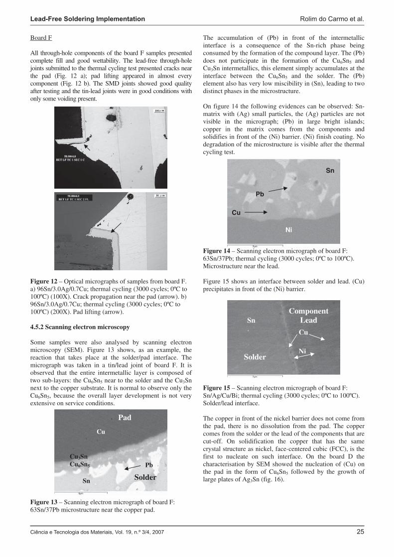
The accumulation of (Pb) in front of the intermetallic
interface is a consequence of the Sn-rich phase being
consumed by the formation of the compound layer. The (Pb)
does not participate in the formation of the Cu6Sn5 and
Cu3Sn intermetallics, this element simply accumulates at the
interface between the Cu6Sn5 and the solder. The (Pb)
element also has very low miscibility in (Sn), leading to two
distinct phases in the microstructure.
On figure 14 the following evidences can be observed: Sn-
matrix with (Ag) small particles, the (Ag) particles are not
visible in the micrograph; (Pb) in large bright islands;
copper in the matrix comes from the components and
solidifies in front of the (Ni) barrier. (Ni) finish coating. No
degradation of the microstructure is visible after the thermal
cycling test.
Figure 14 – Scanning electron micrograph of board F:
63Sn/37Pb; thermal cycling (3000 cycles; 0ºC to 100ºC).
Microstructure near the lead.
Figure 15 shows an interface between solder and lead. (Cu)
precipitates in front of the (Ni) barrier.
Figure 15 – Scanning electron micrograph of board F:
Sn/Ag/Cu/Bi; thermal cycling (3000 cycles; 0ºC to 100ºC).
Solder/lead interface.
The copper in front of the nickel barrier does not come from
the pad, there is no dissolution from the pad. The copper
comes from the solder or the lead of the components that are
cut-off. On solidification the copper that has the same
crystal structure as nickel, face-centered cubic (FCC), is the
first to nucleate on such interface. On the board D the
characterisation by SEM showed the nucleation of (Cu) on
the pad in the form of Cu6Sn5 followed by the growth of
large plates of Ag3Sn (fig. 16).
Pb
Sn
Ni
Cu
Cu
Ni
SnComponent
Lead
Solder
Sn
Pb
Cu
Cu3SnCu6Sn5
Pad
Solder
b

Rolim do Carmo et al. Lead-Free Soldering Implementation
26 Ciência e Tecnologia dos Materiais, Vol. 19, n.º 3/4, 2007
Figure 16 - Scanning electron micrograph of board D. a)
Sn/Ag/Cu eutectic microstructure; b) intermetallics at the
solder/pad interface.
In this characterisation it was also found a very well known
defect: pad lifting.
Figure 17 shows a detail of pad lifting effect and the
consequent crack on the board.
Figure 17 – Scanning electron micrograph of board F:
Sn/Ag/Cu/Bi; Thermal cycling (3000 cycles; 0ºC to 100ºC).
Evident pad lifting (arrow).
The pad lifting phenomenon is due to the mismatch between
the coefficients of thermal expansion (CTE) of the
components during the manufacturing. In table 9 it is shown
the CTE’s of the main constitutive elements of the board’s
components. In this case, the solder is mainly constituted by
tin that has a higher CTE (23.5x10⁻⁶
/K) than the board
(17x10-6
/K). The board expands during soldering, when the
solder solidifies and the board cools down then the solder
contracts more than the board, the pad edges contracts and
can be lifted from the surface of the laminate.
Table 9 – Coefficients of Thermal Expansion of the
different joint materials [8, 13].
Material CTE (x10-6/K)Sn 23.5
Ag 18.9
Cu 17
Ni 13
Pb 29
Cu3Sn 18.4
Cu6Sn5 20
Laminate 17
4.6 Conclusions
In soldering trials carried out at the assembler’s industrial
facilities no major difficulties in the lead-free soldering
process were reported. Especially reflow soldering process
has been carried out with very few problems. Some
soldering defects were experienced with the lead-free
soldered products; namely bridging, solder balls, incomplete
barrel filling. Blistering of some components in board D was
also found. These defects and issues found during the
soldering trials were standard problems, often seen in the
lead processes. Most of them can be attributed to pre-heat
and soldering temperatures in the process. The blistering
found on some components of the board D is due to the
incapability of some components to withstand the higher
lead-free temperatures and/or to the presence of moisture
and consequent poor storage of components.
After the reliability tests, most of the boards passed the
electrical functionality tests, except for the thermal cycled
ones. In general the lead-free joints showed good
performance on the reliability tests carried out. The SMD
(Surface Mount Devices) are less degraded than the through-
hole joints for majority of the tests, this can be due to
assembly process conditions and to expected performance of
the through-hole joints under testing. The through-hole
joints showed more defects than the other regular solders,
like pad lifting, and crack propagation near the pads in
almost all joints after the thermal cycling test. The board D
samples that were submitted to thermal cycling have all
failed the functionality tests. Although some cracks were
found on the joints of the electrolytic capacitors it was not
concluded that the faults come from these cracks, because
these components do not stand the high temperatures
imposed by the thermal cycle test. The lead-free through-
hole joints of the board F samples showed poor
performance, presenting more degradation on the lead-free
joints, especially under the thermal cycling test. This can be
related to the new lead-free wave solder alloy with corrosion
inhibitors used by that company to replace the tin/lead alloy
in the wave solder process.
From the reliability tests and after the characterisation can
be concluded that the lead-free boards showed a good
performance under testing, being equivalent or better than
the tin/lead ones. The defects or anomalies found in most of
the joints result from the manufacture process (voiding and
pad lifting). For the through-hole joints the cracks that can
be seen in some of the samples are always away from the
interface and follow an intergranular fracture mode. The
cracks did not propagate very far in the joint neither through
the intermetallic layer, thus, indicating a good connection
between materials, strong intermetallics, in both tin/lead and
lead-free solders, and it should not compromise the integrity
and functionality of the product.
5. General overview – environmental and economical impact
5.1 Environmental impact and main relevant factors of lead-free soldering
To producers and manufacturers, waste reduction, recovery
and recycling should be and will inevitably be treated as a
long-term goal with an ongoing effort. A product should be
designed for minimal environmental impact with its full
lifecycle in mind. Lifecycle assessment includes all the
Cu6Sn5Ag3Sn

Lead-Free Soldering Implementation Rolim do Carmo et al.
Ciência e Tecnologia dos Materiais, Vol. 19, n.º 3/4, 2007 27
energy and resource inputs to a product, the associated
wastes, and the resulting health and ecological burdens. The
goal is to reduce environmental impacts from cradle to
grave.
Lead is considered to be a cumulative poison; significant
amounts can bring discomfort and disability. Some specific
potential health problems include disorder of the nervous
and reproductive systems, reduced production of
haemoglobin, anaemia and hypertension. The main concerns
related to the use of lead in the industry are:
• Landfill contamination;
• Effluent discharge from the production process;
• Worker’s exposure through fume, dust inhalation and
direct ingestion [11].
The environmental issues bring new concerns to the
produces and manufactures that have to cope with these new
changes. It is this side of the business that has to study and
balance the alternatives in terms of cost and benefit.
Fumes emissions, leaching tests and occupational health
In terms of environmental studies several tests were carried
out in some of the assembler’s facilities. The objective was
to investigate the environmental impact associated with the
lead-free process and waste treatment in manufacturing,
through the evaluation of pollution level involved by the use
of lead-free solder during the assembly processes.
Therefore, three main tests have been carried out in order to
compare the results between the lead and lead-free solders:
• Sampling and analysis of fume emissions;
• Occupational exposure measurements;
• Leaching tests of soldered printed circuits and dross of
the wave processes.
Samples from the reflow, wave and hand soldering
processes, with different solder alloys, have been collected
and analysed. In the environmental measurements carried
out at the companies participating in the project it was
observed that all emission results using lead-free solder
pastes were lower than the obtained with lead containing
alloys. For boards containing lead solders, the lead content
values implies that should be considered as hazardous waste
acceptable only at landfills for hazardous waste. For boards
containing lead-free solders, the values were below the
detection limits and can be considered as inert waste. In the
occupational health measurements, these were under the
limit values for organic compounds and metals in both types
of solders.
5.2 Industrial guidelines for lead-free implementation
5.2.1 Economical study
In terms of economics the lead-free changeover brings big
impacts to the assemblers and manufactures. The RoHS
directive affects areas like: manufacturing, quality, design,
purchasing, marketing, sales, finance and management. The
first question that emerges from this directive is: what do I
need to change/invest to cope with the new demands?
Each producer has to know their own process and some
questions have to be answered:
• Is the present equipment is capable of lead-free
manufacturing, in terms of temperature, process control,
material)?
• Are the current facilities are capable? (separate
manufacturing lines, stocks handling)
• Is new equipment is needed? (Soldering irons, wave
soldering…)
• Is personnel training is needed? (purchasing, technical
staff, engineers, designers)
Regarding equipment issues the wave process is the one that
presents more difficulties due to the bath temperature
increase, increased pre-heat temperatures, flux changes,
longer wave contact time and high contents of tin in the
solders. The following image shows the corrosion of a pot
with lead-free solders where the assembler just removed the
old bath and introduced the lead-free one on the same pot.
The pots have to be prepared to the high contents of tin, new
pots and coatings are available in the market and suitable for
lead-free solders.
Figure 18 – Tin corrosion on a wave soldering machine pot
[18].
The cost of producing is not a simple and straightforward
issue. Many factors contribute for the overall cost:
• Solder product cost;
• Operational cost;
• PCB and component cost;
• Equipment cost;
• System cost.
The solder product cost includes metal elemental price, alloy
compositional cost and production. Metal prices fluctuate
with the market demand and the higher the content of an
expensive metal in the alloy the higher the price of the
solder. Production like ingots, powder, adding flux in the
solder and others, bring indirect costs to the final price of
the solder. The operational costs are different for reflow and
wave. In reflow process using solder paste the main factors
are:
• Electrical consumption for oven operation;
• Reflow oven maintenance;
• PCB change (if applicable);
• Component change (if applicable);
• Machine modification (if applicable);
• Nitrogen usage (if applicable);

Rolim do Carmo et al. Lead-Free Soldering Implementation
28 Ciência e Tecnologia dos Materiais, Vol. 19, n.º 3/4, 2007
In a wave soldering process:
• Solder replenishment required due to dross;
• Solder replenishment required due to compositional
stability;
• Pot stability;
• Electrical consumption;
• PCB change (if applicable);
• Component change (if applicable);
• Machine modification (if applicable);
• Nitrogen usage (if applicable);
• Wave machine maintenance.
PCB and component cost are related mainly to the higher
process temperature required. A change to a different PCB
or component delivering a higher temperature tolerance may
involve additional costs.
Regarding equipment most of the companies did not have
any problems in adapting their reflow ovens to the lead-free
processes, with a good profiling and optimisation the
existing ovens can still be used. In the wave process the
companies found more difficulties due to the higher process
temperatures and two approaches were observed: some
adapt their wave machines for lead-free (e.g. new pots and
other parts), which represent a relatively low investment;
and others calculated the estimated time for failure
(corrosion in the pot, etc), ran the lead-free process in their
old machines and bought a new wave machine at the end of
the calculated lifetime.
The system costs involve the overall assessment of costs:
solder material; process operational cost; component and
PCB cost; equipment cost and amortisation; defects; product
performance and reliability. The defects and reliability of
the product are the most important factors of the system
costs. A product failure is very expensive [19]. Most of the
costs related with lead-free are coming from new
equipments; energy consumption, due to higher
temperatures and re-training the staff.
6. Final conclusions and future work
6.1 Final conclusions
This work presents a brief introduction to the area of
soldering in electronics where a great evolution and effort in
research and development of new solders and equipments
can be seen. The lead-free “obligation” brought a new boost
in this area, leading engineers to discover new solder alloys
with the addition of elements, changing properties and
characteristics, optimising processes.
From the practical part of this work it can be concluded that
the SMEs were prepared for transition and are engaged in
taking this opportunity to reach a higher level of
performance. Some of the companies embraced this
“forced” transition to upgrade and improve their process and
facilities, bringing better capabilities and opportunities in
their businesses. In the Economical chapter (5.2.1) some
factors that should be taken into consideration when
implementing the lead-free process are mentioned. It is
natural that an SME prefers not to invest in new equipment
but the companies present in this study showed that the
purchase of new equipment that is suited and prepared to
run lead-free brought less defects, easier transition, higher
production levels; and on the other hand the companies that
have chosen to adapt their process showed higher defect
levels and more time consumed in tuning up the process.
These factors also bring costs that sometimes are not visible,
it should be the companies’ choice to calculate and decide
whether or not to invest in new equipment. The main issue
found in manufacturing and in reliability of the products is a
component problem, an effort has to be made in order to fit
the components in the lead-free processes and increase their
availability on the market. Components should not only be
RoHS compliant but they have to be able to withstand the
temperatures imposed by the lead-free process.
The defects or anomalies found in most of the assemblers
samples result from the manufacturing process (voiding and
pad lifting). This shows the need for process optimisation
(temperature profiles, fluxing, pre-heating…) in the
manufacturing stage. The wave soldering is by far the most
problematic process.
From the reliability tests it can be concluded that most of the
faults found were due to component failures and not from
the joint integrity. The degradation of both types of solders
is similar, but the operators should be trained to identify the
differences between the lead and lead-free solders. The
inferior wettability and dull aspect of the lead-free alloys
should be taken in account when doing visual inspection,
non trained operators can be misled to classify those
products as defective.
Comparing to the lead process the lead-free soldering
process presented equal or better performance. The
problems found in the new lead-free solders and processes it
should not constitute a major problem in the reliability of
the products. This shows that the lead-free soldering is ready
to be implemented in the small to medium size enterprises,
despite the issues that may be encountered on the way.
These issues can be easily overcome with continuously
process monitoring and tuning up. It is important to keep in
mind that in order to reduce the cost of the soldering process
and increase the reliability of the solder joints, companies
should monitor or continue to monitor their processes and
defects.
This work also allows to conclude that the partnership
between universities, research and development centres and
industry is a must for the evolution and improvement of the
companies processes and products. A lot of work was done
that brought great benefits to this sector.
6.2 Future Work
Following the trend of the electric and electronic
industry and the ELFNET Roadmap [20], some
recommendations for the future work should be approached:
• Thermally compatible components;
• Design for reliability – new tools and processes for high
reliability products;

Lead-Free Soldering Implementation Rolim do Carmo et al.
Ciência e Tecnologia dos Materiais, Vol. 19, n.º 3/4, 2007 29
• High reliability solders – modifications of alloys
(adding ternary elements, nano particles to improve
properties);
• New materials to CTE matching – decrease the CTE’s
differences in a board;
• Improvement in the soldering and de-soldering
processes including rework and repair – new heat
management to mitigate collateral damage (laser
soldering, low temperature soldering, vapour phase
soldering, optimised selective soldering);
• Harmonised reliability standards and data for the lead-
free soldering;
• New technologies for inspection and testing of
components and joints;
• Use of refurbishment material for low cost reliable
reusable components.
7. ACKNOWLEDGEMENTS
The authors are grateful to the partners of the LEADOUT
project that contributed to the work carried out. Thanks to
the SMEs, who have provided the industrial products, as
well as to TWI, Ltd (UK), and INASMET (SP).
8. REFERENCES
[1] Directive 2002/95/EC of the European Parliament and
of the Council of 27 January 2003 on the Restriction of
the use of Certain Hazardous Substances in Electrical
and Electronic Equipment.
[2] Department for Business, Enterprise and Regulatory
Reform. www.berr.gov.uk
[3] Directive 2002/96/EC of the European Parliament and
of the Council of 27 January 2003 on waste Electrical
and Electronic Equipment.
[4] “Transposition of the WEEE and RoHS Directives in
other EU member states”; Government and Legislative
Affairs Consultants – Perchards; 2005.
[5] WEEE Registration and Compliance.
www.weeeregistration.com
[6] European Commission Funded Project – LEADOUT.
www.leadoutproject.com
[7] J. Oliveira Santos, L. Quintino; “Processos de
Soldadura”; Instituto de Soldadura e Qualidade; 1998.
[8] R. Klein Wassink; “Soldering in Electronics”;
Electrochemical Publications; 1989
[9] B. Willis; “Introductory Printed Board Assembly
Guide for Lead-Free Assembly”.
[10] S. Kang; “Microstructure and mechanical properties of
lead-free solders and solder joints used in
microelectronic applications”; IBM J. Res & Dev.;
Vol. 49; No. 4/5; 2005.
[11] J. Hwang; “Environment-Friendly Electronics: Lead-
Free Technology”; Electrochemical Publications Ltd;
2001.
[12] P.Villars, A. Prince, H. Okamoto; “Handbook of
Ternary Alloy Phase Diagrams”; ASM International;
1995.
[13] B. Vandevelde; “Influence of PCB properties on solder
joint fatigue life of assembled IC packages”; European
Microelectronics and Packaging Symposion; 2004.
[14] H. Albrecht; “Interface reactions in microelectronic
solder joints and associated intermetallic compounds:
an investigation of their mechanical properties using
nanoindention”; Electronics Packaging Technology
Conference; 2003.
[15] G. Jang; “The nanoidentation characteristics of
Cu6Sn5, Cu3Sn and Ni3Sn4 intermetallic compounds in
the solder bump.
[16] IPC-A-610D; “Acceptability of Electronic
Assemblies”; IPC Association Connecting Electronics
Industries; 2005.
[17] B. Willis; “Lead-free Defect Guide”; SMART Group.
[18] G. Diepstraten; “Lead-Free and its Effects on
Soldering Process Parameters”; Vitronic Soltec.
[19] J. Hwang; “Implementing lead-free electronics – a
manufacturing guide”; McGraw-Hill; 2004.
[20] ELFNET Roadmap; European Electronics
Interconnection - www.europeanleadfree.net