LCD MODULE SPECIFICATION - · PDF fileThe CT025TN01 is a color active matrix Thin Film...
24
The copyright belongs to InnoLux. Any unauthorized use is prohibited. INNO L U X DISPLAY CORPORATION LCD MODULE SPECIFICATION Customer: Model Name: CT025TN01 Spec. No.: C025-01-TT-01 Data: 2008/01/02 Version: 04 □ Preliminary Specification ■ Final Specification For Customer’s Acceptance Approved by Comment Approved by Reviewed by Prepared by Rock Chi 2008/01/10 Jack Huang 2008/01/07 Kevin Chen 2008/01/07
Transcript of LCD MODULE SPECIFICATION - · PDF fileThe CT025TN01 is a color active matrix Thin Film...
The copyright belongs to InnoLux. Any unauthorized use is prohibited.
INNOLUX DISPLAY CORPORATION LCD MODULE
SPECIFICATION
Customer: Model Name: CT025TN01 Spec. No.: C025-01-TT-01 Data: 2008/01/02 Version: 04
Preliminary Specification
Final Specification
For Customer ’s Acceptance
Approved by Comment
Approved by Reviewed by Prepared by
Rock Chi
2008/01/10
Jack Huang
2008/01/07
Kevin Chen
2008/01/07
The copyright belongs to InnoLux. Any unauthorized use is prohibited.
Record of Revision
Version Revise Date Page Content
Pre-SPEC 01 2007/02/16 All Initial release
02 2007/02/27 1,6,13 Color arrangement change to RGB-stripe
03 2007/04/19 2 Update Block Diagram
3 Update Pin Assignment
15 Update Mechanical Drawing
04 2007/06/15 1 Update General Specifications
2 Update Block Diagram
5~9 Update Electrical Specifications
8 Update VDD
12 Add the tolerance of the white Color chromaticity
19 Update the lable of Mechanical Drawing
Final-SPEC 01 2007/07/04 1 Update General Specifications
3 Modify Pin 7 from NC to VCOMH
Add remark for pin 7 and pin 8
12 Add Min. Values of Color Gamut
Add Min. Values of Luminance Uniformity
Add Min. Values of Viewing Angle
17 Update Note1 and Note2
19 Add DC number of the Mechanical Drawing
20,21 Add Package Drawing
02 2007/08/16 8 Add Power on sequence
03 2007/12/07 1 Modify Weight Specification
14 Modify Fig. 1 Definition of uniformity 16 Modify Fig. 2 Definition of viewing direction for display 19 Modify Mechanical Drawing
20 Modify Weight Specification
04 2008/01/02 19 Modify Mechanical Drawing
The copyright belongs to InnoLux. Any unauthorized use is prohibited.
Contents 1. General Specifications........................................................................................................... 1
2. Block Diagram ....................................................................................................................... 2
3. Pin Assignments.................................................................................................................... 3
4. Electrical Specifications......................................................................................................... 5
4.1. Absolute Maximum Ratings............................................................................................. 5
4.2.Typical Operation Conditions ........................................................................................... 5
4.3.Backlight Unit (LED Type) ................................................................................................ 7
4.4.Instruction List.................................................................................................................. 7
4.5.Instruction Setting Flow.................................................................................................... 8
4.6.Timing Characteristics...................................................................................................... 9
4.6.1 SPI Interface Timing...................................................................................................... 9
4.6.2 Parallel RGB Interface Timing..................................................................................... 10
5. Optical Specifications .......................................................................................................... 12
6. Reliability Test Items............................................................................................................ 17
7. Handling Precautions .......................................................................................................... 18 7.1 Safety............................................................................................................................. 18
7.2.Handling......................................................................................................................... 18
7.3.Static Electricity .............................................................................................................. 18
7.4.Storage........................................................................................................................... 18
7.5.Cleaning......................................................................................................................... 18
8 Mechanical Drawing ............................................................................................................ 19
9 Package Drawing ................................................................................................................ 20
9.1.Packaging Material Table ............................................................................................... 20
9.2.Packaging Quantity ........................................................................................................ 20
9.3.Package Drawing........................................................................................................... 21

SPEC.NO.: C025-01-TT-04 PAGE: 1/21
The copyright belongs to InnoLux. Any unauthorized use is prohibited
1. General Specifications 1.1. Description
The CT025TN01 is a color active matrix Thin Film Transistor (TFT) Liquid Crystal Display (LCD) that uses amorphous silicon (a-Si) TFT as a switching device. This module is composed of a single 2.5 inches transmissive type main TFT-LCD Panel. The resolution of the panel is 320x240 pixels and can display 262K color.
1.2. Features:
-TM type for main TFT-LCD panel
-One backlight with 3 white LED
-RGB interface
-Full, Still & Standby mode are available
1.3. Application:
-Display terminals for host computer
1.4. General Specifications
No. Item Specification Unit Remark
1 LCD Size 2.5 (diagonal)(landscape) Inch -
2 Panel Type a-Si TFT - -
3 Resolution 320(RGB) x 240 Pixel -
4 Display Mode Normally white, Transmissive - -
5 Display Number of Colors 262 K - -
6 Viewing Direction 12 o’clock - Note 1
7 Module Size 56.40(W) x 49.12(L) x 2.70(T) mm Note 1
8 Active Area 49.92(W) x 37.44(L) mm -
9 Pixel Pitch 52 x 156 um -
10 Weight 15.4 g -
11 Color Arrangement RGB Stripe - -
12 Polarizer Surface Treatment Hard Coating - -
13 Driver IC ILI9322 - -
14 Light Source 3 white LEDs - -
15 Interface RGB - -
Note 1: Refer to mechanical drawing.
SPEC.NO.: C025-01-TT-04 PAGE: 2/21
The copyright belongs to InnoLux. Any unauthorized use is prohibited
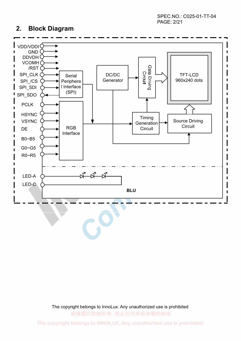
2. Block Diagram
TFT-LCD960x240 dots
Source Driving CircuitRGB
Interface
DC/DC Generator
Timing Generation
Circuit
GND
SPI_/CS
B0~B5
G0~G5R0~R5
HSYNC
VDD/VDDI
BLULED-C
LED-A
SPI_SDI
Serial Peripheral Interface
(SPI)
VSYNC
DE
PCLK
SPI_CLK/RST
DDVDH
SPI_SDO
VCOMH

SPEC.NO.: C025-01-TT-04 PAGE: 3/21
The copyright belongs to InnoLux. Any unauthorized use is prohibited
3. Pin Assignments (ZIF Molex SD-54393-3918)
Pin No. Symbol I/O Function Remark
1 LED-A P Anode for LEDs -
2 LED-C P Cathode for LEDs -
3 VDDI P Voltage input for I/O logic -
4 VDD P Voltage supply pin for analog circuit -
5 GND P Ground -
6 GPIO P Ground -
7 VCOMH P Test pad for OTP Only for Innolux
8 DDVDH P Power supply for OTP Only for Innolux
9 NC - - -
10 SPI_/CS I Chip select pin of serial interface -
11 SPI_SDI I Data input pin in serial mode -
12 SPI_SDO O Data output pin in serial mode -
13 SPI_CLK I Clock pin of serial interface -
14 NC - - -
15 /RST I Reset Signal Pin -
16 B0 I Blue Data (Bit 0) -
17 B1 I Blue Data (Bit 1) -
18 B2 I Blue Data (Bit 2) -
19 B3 I Blue Data (Bit 3) -
20 B4 I Blue Data (Bit 4) -
21 B5 I Blue Data (Bit 5) -
22 G0 I Green Data (Bit 0) -
23 G1 I Green Data (Bit 1) -
24 G2 I Green Data (Bit 2) -
25 G3 I Green Data (Bit 3) -
26 G4 I Green Data (Bit 4) -
27 G5 I Green Data (Bit 5) -
28 R0 I Red Data (Bit 0) -
29 R1 I Red Data (Bit 1) -
30 R2 I Red Data (Bit 2) -
31 R3 I Red Data (Bit 3) -
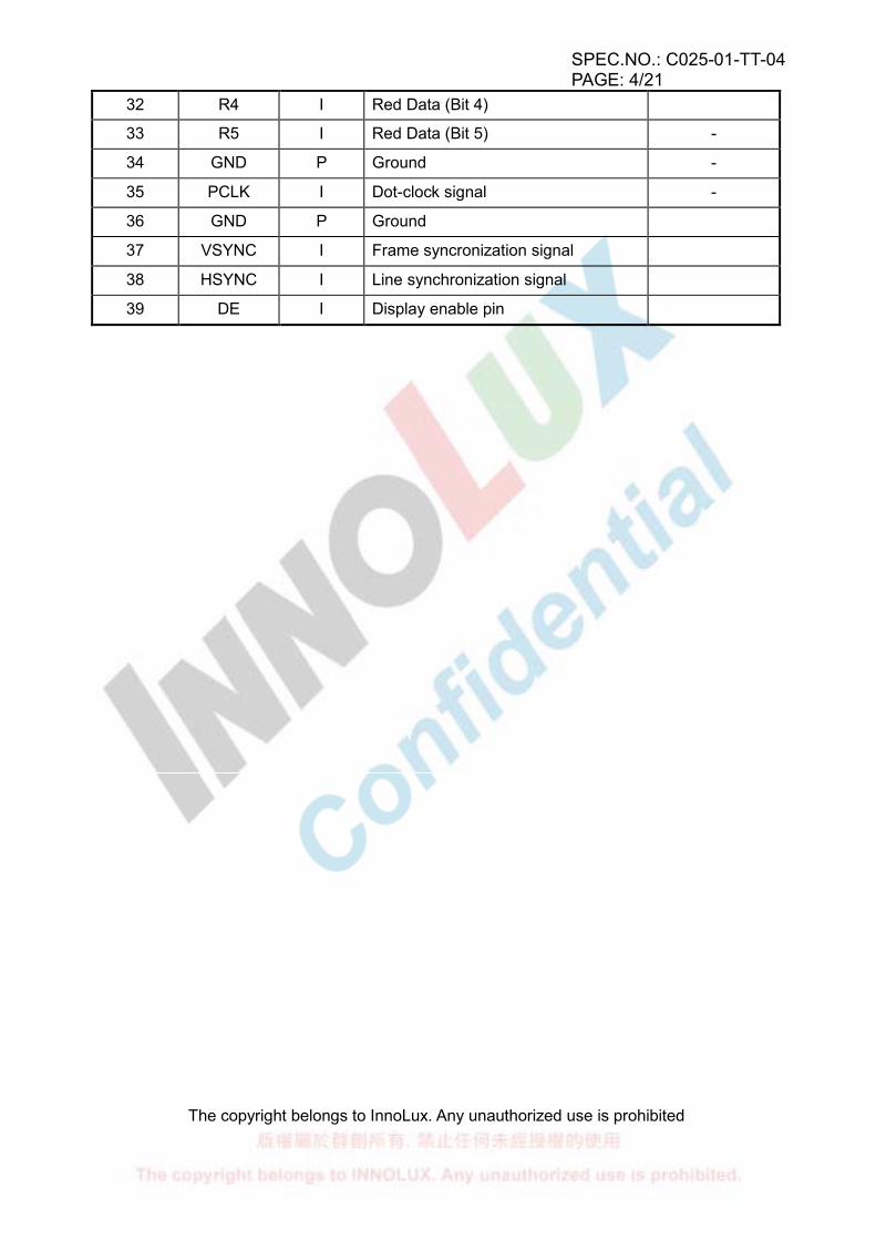
SPEC.NO.: C025-01-TT-04 PAGE: 4/21
The copyright belongs to InnoLux. Any unauthorized use is prohibited
32 R4 I Red Data (Bit 4)
33 R5 I Red Data (Bit 5) -
34 GND P Ground -
35 PCLK I Dot-clock signal -
36 GND P Ground
37 VSYNC I Frame syncronization signal
38 HSYNC I Line synchronization signal
39 DE I Display enable pin

SPEC.NO.: C025-01-TT-04 PAGE: 5/21
The copyright belongs to InnoLux. Any unauthorized use is prohibited
4. Electrical Specifications 4.1. Absolute Maximum Ratings
Values Item Symbol Min. Max.
Unit Remark
Logic Supply Voltage VDDI -0.3 +4.6 V Note 1 TFT Module
Analog Supply Voltage VDD -0.3 +4.6 V Note 1
Current IB - 30 mA Note 2 Backlight Unit
Power Consumption PBL - 324 mW Note 2
Note1: Permanent damage to the device may occur if maximum values are exceeded or reverse voltage is applied.
Note2: Without LED driver IC, please refer to 4.3.
4.2.Typical Operation Conditions 4.2.1 DC Characteristics
(Ta=+25к, VDD =+3.3V)
Values
Item Symbol
Min. Typ. Max. Unit Remark
Logic Supply Voltage VDDI 3.13 3.3 3.46 V
Analog Supply Voltage VDD 3.13 3.3 3.46 V
Input High Voltage VIH 0.7VDDI - VDDI V
Input Low Voltage VIL GND - 0.3VDDI V
Output High Voltage VOH GND - - V
Output Low Voltage VOL VDDI-0.4 - VDDI V
Frame Frequency fFRAME - 70 - HZ
Ta=25к
Note: To prevent IC latch up or DC operation in LCD panel, the power on/off sequence should
follow the driver IC specification.
SPEC.NO.: C025-01-TT-04 PAGE: 6/21
The copyright belongs to InnoLux. Any unauthorized use is prohibited
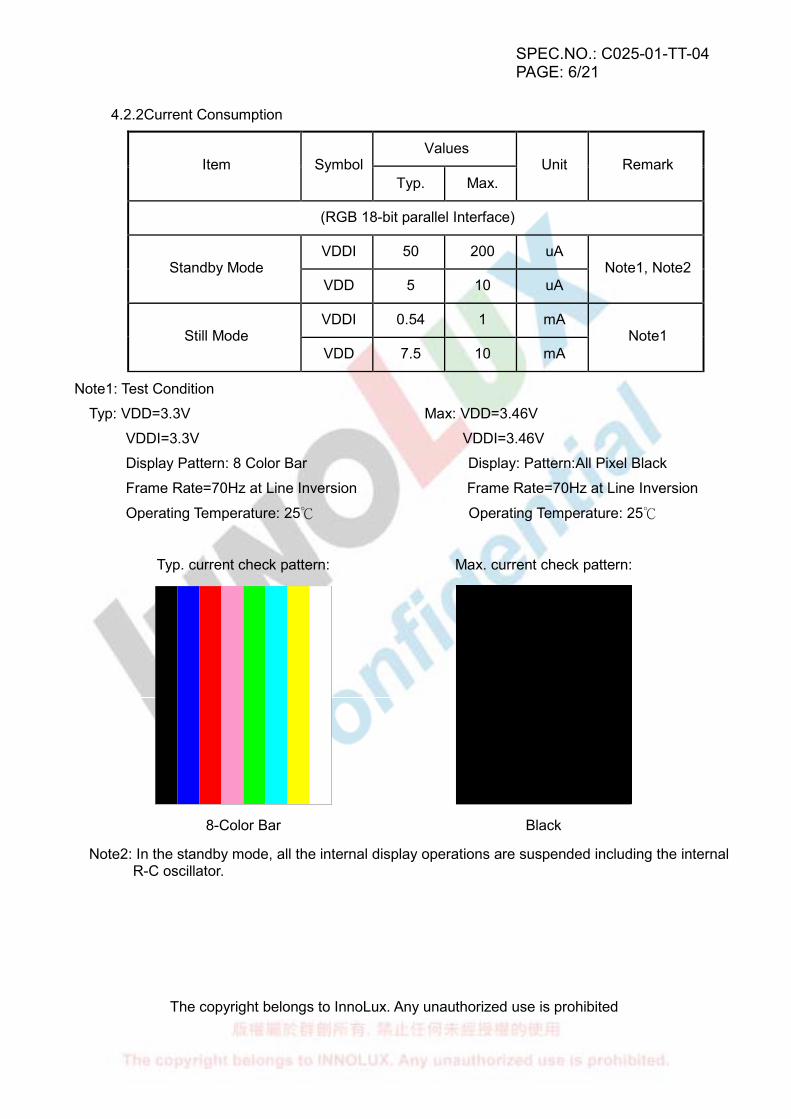
4.2.2Current Consumption
Values Item Symbol
Typ. Max. Unit Remark
(RGB 18-bit parallel Interface)
VDDI 50 200 uA Standby Mode
VDD 5 10 uA Note1, Note2
VDDI 0.54 1 mA Still Mode
VDD 7.5 10 mA Note1
Note1: Test Condition
Typ: VDD=3.3V Max: VDD=3.46V
VDDI=3.3V VDDI=3.46V
Display Pattern: 8 Color Bar Display: Pattern:All Pixel Black
Frame Rate=70Hz at Line Inversion Frame Rate=70Hz at Line Inversion
Operating Temperature: 25к Operating Temperature: 25к
Typ. current check pattern: Max. current check pattern:
8-Color Bar Black
Note2: In the standby mode, all the internal display operations are suspended including the internal R-C oscillator.

SPEC.NO.: C025-01-TT-04 PAGE: 7/21
The copyright belongs to InnoLux. Any unauthorized use is prohibited
4.3.Backlight Unit (LED Type) The backlight system is an edge lighting type with 3 white LEDs.
Values Item Symbol
Min. Typ. Max. Unit Remark
Current IB - 20 - mA Note 1
Power Consumption PBL - 217.5 - mW Note 1,2
Note1: 3 LEDs are connected in serial; LED current consumption is 20 mA
Note2: Where IB= 20mA, PBL = IB x VBL
4.4.Instruction List
Register Description Value Remark
R01 VCOM Amplitude 0x0F - R02 VCOM High Voltage 0x2C - R03 VREG1OUT Voltage 0x0B - R05 Power Setting 0x25 - R06 Entry Control 0x6C - R07 Power Control 0xEF - R08 Vertical Back Porch 0x11 - R09 Horizontal Back Porch 0x80 - R0A Polarity 0x49 - R0B Display 0x01 - R0C DC/DC 0x24 - R0D Driving 0x0A - R0E CONTRAST 0x08 - R0F BRIGHT 0x82 - R10 Gamma1 0x6B - R11 Gamma2 0x6F - R12 Gamma3 0x69 - R13 Gamma4 0x68 - R14 Gamma5 0x6A - R15 Gamma6 0x5C - R16 Gamma7 0x6F - R17 Gamma8 0x5B - R30 Power 0x09 -
R42 OTP Program 0x40 -
VBL
IB

SPEC.NO.: C025-01-TT-04 PAGE: 8/21
The copyright belongs to InnoLux. Any unauthorized use is prohibited
4.5. Instruction Setting Flow Power ON Sequence Power OFF Sequence
Power on sequence
ˣ ˸ ʳ ˢ ˹ ˹ ʳ ˦ ˸ ˼ ˺ʻ ˥ ˃ ˊ ˻ ː ˃ ˘ ˘ ʳ ʳ ˦ ˧ ˕ ʳ ˼ ː ˟ ʼ
˪ ˴ ˼ ʳ ˴ ʳ ˿ ˸ ˴ ʳ ˈ ʳ ˹ ˴ ˸
˗ ˖ ˟ ˞ ʳ ˦
˗ ˼ ˿ ˴ ʳ ˢ ˹ ˹
˦ ˸ ʳ ˣ ˸ ʳ ˢ
˪ ˴ ˼ ʳ ˅ ˃
˥ ˸ ˸ ʳ ˜ ˟ ˜ ˌ ˆ ˅ ˅
˜ ˸ ˹ ˴ ˶ ˸ ʳ ˼ ˺ ˴ ˿˦ ˴ ʳ
˪ ˴ ˼ ʳ ˄ ˃
ˣ ˸ ʳ ˢ ʳ ˦ ˸ ˼ ˺ʻ ˥ ˃ ˊ ˻ ː ˃ ˘ ˙ ʳ ʳ ˦ ˧ ˕ ʳ ˼ ː ˛ ˼ ˺ ˻ ʼ
˥ ˸ ˺ ˼ ˸ ʳ ˦ ˸ ˼ ˺
˪ ˴ ˼ ʳ ˄ ˃ ʳ ʳ ˋ ˃ ʳ ˹ ˴ ˸
˗ ˼ ˿ ˴ ʳ ˢ

SPEC.NO.: C025-01-TT-04 PAGE: 9/21
The copyright belongs to InnoLux. Any unauthorized use is prohibited
Standby Mode Sequence
4.6.Timing Characteristics 4.6.1 SPI Interface Timing
Serial Peripheral Interface (SPI) Timing Characteristics
Item Symbol Min. Typ. Max. Unit
Setup Time tCS 50 - - SPI_/CS to CLK Hold Time tCE 50 - -
ns
SPI_CLK Period tSCK 50 - - ns
SPI_CLK High Period tSKH 25 - - ns
SPI_CLK Low Period tSKL 25 - - ns
SPI_SDI Data Setup Time tSU 15 - - ns
SPI_SDI Data Hold Time tHD 15 - - ns
SPI_/CS High Pulse Period tCH 50 - - ns
˘˸ ʳ˼ʳ ˴ ˷˵ʳ˷˸
˪˴ ˼ʳ˴ ʳ˿˸ ˴ ʳˈʳ˹˴˸
˗˖˟˞ʳ˦
˦ ˴ ˷˵
ˣ ˸ ʳˢ˹˹ʳ˦ ˸ ˼˺ʻ˥˃ˊ˻ː˃˘˘ʳʳ˦ ˧˕ʳ˼ː˟ʼ
˘˼ʳ˹ʳ ˴ ˷˵ʳ˷˸
ˣ ˸ ʳˢ˹˹ʳ˦ ˸ ˼˺ʻ˥˃ˊ˻ː˃˘˙ʳʳ˦ ˧˕ʳ˼ː˛˼˺˻ʼ
˪˴ ˼ʳ˴ ʳ˿˸ ˴ ʳ˄˃ʳʳˋ˃ʳ˹˴˸
ˡ˴ ˿ʳ˸ ˴ ˼
˗˖˟˞ʳ˦ ˴

SPEC.NO.: C025-01-TT-04 PAGE: 10/21
The copyright belongs to InnoLux. Any unauthorized use is prohibited
˔ˉ ˔ˈ ˔ˇ ˔ˆ ˔˅ ˔˄ ˔˃ ˗ˊ ˗ˉ ˗ˈ ˗ˇ ˗ˆ ˗˅ ˗˄ ˗˃˥˂˪˦ ˣ ˜˲˦˗˜
˦ ˣ ˜˲˖˟˞
˦ˣ ˜˲˂˖˦
˖˦ ˦˖˞ ˦˞˛
˦˞˟
˖˘
˖˛
˦˨ ˛˗
˥˂˪ʳːʳ˄ʳʿʳ˥˸˴˷ʳˠ˷˸ʳ˥˂˪ʳːʳ˃ʳʿʳ˪˼˸ʳˠ˷˸
4.6.2 Parallel RGB Interface Timing
RGB Digital Timing Characteristics
Parameter Symbol Min. Typ. Max. Unit. Note
DCLK Frequency 1/tDCLK - 6.4 10 MHz -
Period tH 360 408 - tDCLK -
Display Period tHD 320 320 320 tDCLK -
Back Porch tHB 38 38 - tDCLK -
Front Porch tHF 12 50 - tDCLK -
HSYNC
Pulse Width tHP 1 1 - tDCLK -
Period tV 244 262 - tH -
Display Period tVD 240 240 240 tH -
Back Porch tVB 2 18 - tH -
Front Porch tVF 2 4 - tH -
VSYNC
Pulse Width tVP 1 1 - tH -
Data setup time tSU 12 - - ns -
Data hold time tHOLD 12 - - ns -

SPEC.NO.: C025-01-TT-04 PAGE: 11/21
The copyright belongs to InnoLux. Any unauthorized use is prohibited
˩˦ˬˡ˖
˛˦ˬˡ˖
˗˘
˂˂˂˂˂˂˂˂
˵
˹˷
˄˛
˂˂˂˂˂˂˂˂
˂˂˂˂˂˂˂˂
˛˦ˬˡ˖
˗˘
˗ˮ ˍ˃˰ ˼˴ ˿˼˷ ˄ ʳ˿˼ ˸ ˅˷ʳ˿˼˸ ˆ˷ʳ˿˼˸ ˿˴ ʳ˿˼˸ ˼˴ ˿˼˷
˛˦ˬˡ˖
˗˖˟˞˂˂˂˂˂˂˂˂
˻
˻˵
˻
˻˹˻˷
˄˂˗˖˟˞
˂˂˂˂˂˂˂˂
˗˘˂˂˂˂˂˂˂˂
˂˂˂˂˂˂˂˂
˂˂˂˂˂˂˂˂˥˄ ˥˅
˥ˆ˅˃
˼˴ ˿˼˷˼˴ ˿˼˷˗˃ˮ ˍ˃˰ ˥ˆ ˥ˇ
˂˂˂˂˂˂˂˂
˂˂˂˂˂˂˂˂˚˄ ˚˅
˚ˆ˅˃
˼˴ ˿˼˷˼˴ ˿˼˷˗˄ˮˊˍ˃˰ ˚ˆ ˚ˇ
˂˂˂˂˂˂˂˂
˂˂˂˂˂˂˂˂˕˄ ˕˅
˕ˆ˅˃
˼˴ ˿˼˷˼˴ ˿˼˷˗˅ˮˊˍ˃˰ ˕ˆ ˕ˇ
˥ˆ˄ˌ
˚ˆ˄ˌ
˕ˆ˄ˌ
˥ˈ
˚ˈ
˕ˈ
˗˖˟˞
˕˿˴˾˼˺ʳ˷˴ ˴
˕˿˴ ˾˼˺ʳ˷˴ ˴
˕˿˴ ˾˼˺ʳ˷˴ ˴
˻˿˷
˗˖˟˞
˗˃ˮˊˍ˃˰
˗˄ˮˊˍ˃˰
˗˅ˮˊˍ˃˰
˥˄ ˥˅ ˥ˆ ˥ˇ ˥ˈ
˚˄
˕˄
˚˅
˕˅
˚ˆ
˕ˆ
˚ˇ
˕ˇ
˚ˈ
˕ˈ
˗˘
˥ˉ
˚ˉ
˕ˉ

SPEC.NO.: C025-01-TT-04 PAGE: 12/21
The copyright belongs to InnoLux. Any unauthorized use is prohibited
5. Optical Specifications (Ta=+25 , VDD=+к 3.3V, IB=20mA)
Values Item Symbol Condition
Min. Typ. Max. Unit Remark
Response time Ton +Toff Normal θ=Ф=0˚ - 30 50 ms Note 2
Contrast ratio CR At optimized viewing angle
150 250 - - Note 3
Luminance L Normal θ=Ф=0˚ 200 250 - cd/m2 Note 4,6
Wx 0.26 0.31 0.36 Color chromaticity (CIE1931)
White Wy
Normal θ=Ф=0˚ 0.28 0.33 0.38
- Note 5,6
Left ФL 40 45 -
Right ФR 40 45 -
Top ФT 50 55 - Viewing angle
Bottom ФB
CR 10Њ
10 15 -
Degree Note 10
Color Gamut CIE1931 40 50 - % -
Luminance uniformity UL Normal θ=Ф=0˚ 70 75 - % Note 7
Flicker - Not visible - Note 8
Cross talk - Not visible - Note 9

SPEC.NO.: C025-01-TT-04 PAGE: 13/21
The copyright belongs to InnoLux. Any unauthorized use is prohibited
Note 1: Definition of optical measurement system. The optical characteristics should be measured in dark room and with ambient temperature Ta=25C. After 30 minutes operation, the optical properties are measured at center point of the LCD screen. (Equipment: Photo detector TOPCON BM-5A or BM-7 /Field of view: 1˚ /Height: 500mm.)
Photo detector
Ф=270˚
6 o’clock direction
Fig. 1 Optical measurement system setup
Note 2: Definition of response time The response time is defined as the LCD optical switching time interval between “White” state and
“Black” state. Rise time (TON) is the time between photo detector output intensity changed from 90% to 10%. And fall time (TOFF) is the time between photo detector output intensity changed from 10% to 90%.
Fig. 2 Definition of response time
100% 90%
10% 0%
Ф=270˚
6 Ф=180˚
Ton Toff
White (TFT OFF)
Black (TFT ON)
White (TFT OFF)
500mm
Ф=180˚ Active Area
LCD Panel
12 o’clock direction Ф=90˚
Normal line θ=Ф=0˚
Ф=0˚

SPEC.NO.: C025-01-TT-04 PAGE: 14/21
The copyright belongs to InnoLux. Any unauthorized use is prohibited
Note 3: Definition of contrast ratio
state Black"" the on LCD whenmeasured Luminancestate White"" the on LCD whenmeasured Luminance
(CR) ratio Contrast =
Note 4: Definition of luminance: Luminance of “white” state measured at the center point of LCD.
Note 5: Definition of color chromaticity (CIE1931). Color coordinates measured at the center point of LCD when panel is driven at “White” state respectively.
Note 6: Measured at the center area of the panel when all the input terminals of LCD panel are electrically opened.
Note 7: Definition of uniformity: To test for uniformity, the tested area is divided into 3 rows and 3 columns. The measurement spot is placed at the center of each box.
Luminance Uniformity (UL) =max
min
LL
W-------Active area width L----- Active area length
W
L
W/6 W/3 W/3
L/6
L/3
L/3
Fig. 3 Definition of uniformity
maxL : The measured maximum luminance of all measurement position.
minL : The measured minimum luminance of all measurement position.

SPEC.NO.: C025-01-TT-04 PAGE: 15/21
The copyright belongs to InnoLux. Any unauthorized use is prohibited
Note 8: Definition of flicker: There should be no visible flicker in the display when the following figures are loaded.
Fig. 4 Flicker check pattern
Note 9: Definition of crosstalk: There should be no visible crosstalk in normal direction of the display when the following figures are loaded
Fig. 5 Crosstalk check pattern

SPEC.NO.: C025-01-TT-04 PAGE: 16/21
The copyright belongs to InnoLux. Any unauthorized use is prohibited
Note 10: Definition of viewing angle range
Fig. 6 Definition of viewing angle
Fig. 7 Definition of viewing direction for display
θB
Left
Bottom
Right
Normal line θ=Φ=0°
Φ=270°
6 o’clock direction
Φ=0° Φ=180°
Active Area
θL θT
θB θR
Φ=90°
12 o’clock direction

SPEC.NO.: C025-01-TT-04 PAGE: 17/21
The copyright belongs to InnoLux. Any unauthorized use is prohibited
6. Reliability Test Items (Note1)
Test Items Test Conditions Remark
High Temperature Storage +70 ±3 for 240 hoursк к Note2
Low Temperature Storage -20 ±3 for 240 hoursк к Note2 High Temperature Operation +60 ±3 for 240 hoursк к Note2
Low Temperature Operation -10 ±3 for 240 hoursк к Note2
Operate at High Temperature and Humidity +60 ±3 , 90%±3%RH max. for 240 hoursк к Note2
Thermal Shock -20к/0.5h ~ +70 /0.5h for a total 100 cycles, кStart with cold temp and end with high temp Note2
Vibration Test
Frequency range:10~55Hz Stoke:1.5mm Sweep:10Hz~55Hz~10Hz 2 hours for each direction of X. Y. Z. (6 hours for total)
JIS C7021 A-10 Condition A
Mechanical Shock 100G 6ms,±X, ±Y, ±Z 3 times for each direction
JIS C7021 A-7 Condition C
Package Vibration Test
Random Vibration : 0.015G2/Hz from 5-200Hz, -6dB/Octave from 200-500Hz 2 hours for each direction of X. Y. Z. (6 hours for total)
IEC 68-34
Package Drop Test Height:72cm(Weight 10kg);Љ 60cm(Weight 10kg)Њ 1 corner, 3 edges, 6 surfaces
JIS Z0202
Electro Static Discharge ± 2KV, Human Body Mode, 100pF/1500Ω, LCM Power ON
Note1: In the standard condition, there shall be no practical problem that may affect the display function. After the reliability test, the product only guarantees operation, but doesn't guarantee all the cosmetic specification.
Note2: Before cosmetic and function tests , the product must have enough recovery time,at least 2 hours at room temperature.

SPEC.NO.: C025-01-TT-04 PAGE: 18/21
The copyright belongs to InnoLux. Any unauthorized use is prohibited
7. Handling Precautions 7.1 Safety 7.1.1The liquid crystal in the LCD is poisonous. DO NOT put it in your mouth. If the liquid crystal
touches your skin or clothes, wash it off immediately using soap and water.
7.2.Handling 7.2.1.The LCD panel is plate glass. DO NOT subject the panel to mechanical shock or to excessive
force on its surface.
7.2.2.The polarizer attached to the display is very easy to damage, handle it with careful attention.
7.2.3.To avoid contamination on the display surface, DO NOT touches the display surface with bare hands.
7.2.4.Provide a space so that the LCD panel does not come into contact with other components.
7.2.5.To protect the LCD panel from external pressure, put covering glass (acrylic board or similar board) keeping appropriate gap between them.
7.2.6.Transparent electrodes may be disconnected if you use the LCD panel under environmental conditions where dew condensation occurs.
7.2.7.Property of semiconductor devices may be affected when they are exposed to light, possibly resulting in malfunctioning of the ICs.
7.2.8.To prevent such malfunctioning of the ICs, your design and mounting layout done are so that the IC is not exposed to light in actual use.
7.3.Static Electricity 7.3.1.Ground soldering iron tips, tools and testers when you operate.
7.3.2.Ground your body when handling the products.
7.3.3.DO NOT apply voltage to the input terminal without applying power supply.
7.3.4.DO NOT apply voltage which exceeds the absolute maximum rating.
7.3.5.Store the products in an anti-electrostatic container.
7.4.Storage 7.4.1.Store the products in a dark place at +25 ±10 , low humidity (65%RH or less).к к
7.4.2.DO NOT store the products in an atmosphere containing organic solvents or corrosive gases.
7.5.Cleaning 7.5.1DO NOT wipe the polarizer with dry cloth, as it might cause scratch.
7.5.2Wipe the polarizer with a soft cloth soaked with petroleum IPA, other chemical might damage.
SPEC.NO.: C025-01-TT-04 PAGE: 19/21
The copyright belongs to InnoLux. Any unauthorized use is prohibited
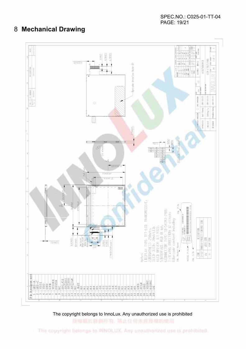
8 Mechanical Drawing Pin Assignment
1 2 3 4 5 6 7 8 9 10 11 12 13 14 15 16 17 18 19 20 21 22 23 24 25 26 27 28 29 30 31 32 33 34 35
GPIO
36 37 38 39
LED-
ALED-
CVD
DIVD
D
SPI_SD
ISP
I_SD
OSP
I_CL
K
R2 R3 R4 R5 PCLK
GND VSYN
CHS
YNC
DENC /RST
B0 G0
G1
G2
G3
G4
G5
R0 R1 GNDGND VCOMH
DDVD
HNC SP
I_/CS
B1 B2 B3 B4 B5

SPEC.NO.: C025-01-TT-04 PAGE: 20/21
The copyright belongs to InnoLux. Any unauthorized use is prohibited
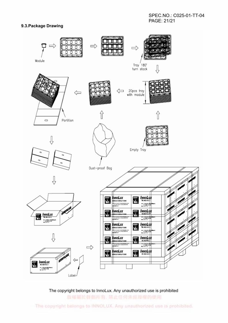
9 Package Drawing 9.1.Packaging Material Table
Per Carton
No Item Model (Material) Dimensions(mm) Unit Weight(Kg) Quantity Remark
1 LCM module CT025TN01 56.4×49.12×2.7 0.015 480
2 Tray PE 345×245×18 0.090 42 Anti-static
3 Dust-Proof Bag PE 410×365×0.8 0.048 2
4 Partition Corrugated Paper 340×254×230 0.220 2
5 Carton Corrugated Paper 530×355×255 1.100 1
6 Total weight 12.800kg±5%
9.2.Packaging Quantity
(1) LCM quantity in per Tray: 12 pcs
(2) Total LCM quantity in per Carton: 2 set x 12pcs per tray x20 pcs tray = 480pcs
SPEC.NO.: C025-01-TT-04 PAGE: 21/21
The copyright belongs to InnoLux. Any unauthorized use is prohibited
9.3.Package Drawing


![Requirements for the floating structure (Demo 1) · [R05] IEC 61400-3 “Wind turbines: design requirements for offshore wind turbines” [R06] “ode for construction and equipment](https://static.fdocuments.in/doc/165x107/60723a69583caa4770307f37/requirements-for-the-floating-structure-demo-1-r05-iec-61400-3-aoewind-turbines.jpg)