LCD Datasheet By · PDF fileFig9à9ÚInput/Output signal waveforms 22 ......
33
LQ065T5AR01 Color TFT LCD Module (Model Number: LQ065T5AR01) Specifications Spec No.: LCY-01096B Dated: May 31. 2002
Transcript of LCD Datasheet By · PDF fileFig9à9ÚInput/Output signal waveforms 22 ......

LQ065T5AR01 Color TFT LCD Module
(Model Number: LQ065T5AR01)
Specifications
Spec No.: LCY-01096B
Dated: May 31. 2002

PREPARED BY: DATE SPEC No. LCY-01096B
FILE No.
APPROVED BY: DATE ISSUE: Jan. 24. 2002
PAGE : 29 pages
MOBILE LIQUID CRYSTAL
DISPLAY GROUP
SHARP CORPORATION
SPECIFICATIONSPECIFICATIONSPECIFICATIONSPECIFICATION
APPLICABLE GROUP
LIQUID CRYSTAL DISPLAY GROUP
DEVICE SPECIFICATION FOR
TFT TFT TFT TFT 㵨㵨㵨㵨 LCD module LCD module LCD module LCD module
MODEL No. LQ065T5AR01MODEL No. LQ065T5AR01MODEL No. LQ065T5AR01MODEL No. LQ065T5AR01
CUSTOMER'S APPROVAL
DATE
PRESENTED
BY BY
S.YASUDA
Department General manager
Engineering department 㸈
Mobile LCD design cen䌴er
MOBILE LIQUID CRYSTAL DISPLAY GROUP
SHARP CORPORATION
RECORDS OF REVISION 㧹㧻㧰㧱㧸 㧺㨛㧦㧸㧽㧜㧢㧡㨀㧡㧭㧾㧜㧝
SPEC No. DATE REVISED
No. PAGE
SUMMARY NOTE
LCY-01096 2001.11. 9. - - 1 st Issue
2001.12.18 A 3 add a postscript(Fig.7)
8 change temperature of Absolute maximum
ratings.(Ta=25͠ψ-30㨪+85͠)
15,19 change protection film
16 correct a error word(Fig.7ψFig.8)
19 add a postscript(depth of mounting hole)
2002.01.24 B - change PWB for improve of coupling issue
(DUNTK2959TPZZ ψ DUNTK3028TPZZ)

LCY01096㧙1
NOTICE
This publication is the proprietary of SHARP and is copyrighted, with all rights reserved. Under the copyright laws, no part of this publication may be reproduced or transmitted in any form or by any means, electronic or mechanical for any purpose, in whole or in part, without the express written permission of SHARP. Express written permission is also required before any use of this publication may be made by a third party. The application circuit examples in this publication are provided to explain the representative applications of SHARP's devices and are not intended to guarantee any circuit design or permit any industrial property right or other rights to be executed. SHARP takes no responsibility for any problems related to any industrial property right or a third party resulting from the use of SHARP's devices, except for those resulting directly from device manufacturing processes. In the absence of confirmation by device specification sheets, SHARP takes no responsibility for any defects that occur in equipment using any of SHARP's devices, shown in catalogs, data books, etc. Contact SHARP in order to obtain the latest device specification sheets before using any SHARP's device. SHARP reserves the right to make changes in the specifications, characteristics, data, materials, structures and other contents described herein at any time without notice in order to improve design or reliability. Contact SHARP in order to obtain the latest specification sheets before using any SHARP's device. Manufacturing locations are also subject to change without notice. Observe the following points when using any device in this publication. SHARP takes no responsibility for damage caused by improper use of the devices. The devices in this publication are designed for use in general electronic equipment designs,such as: Automotive auxiliary information display Car Navigation system Automotive audio visual equipment The appropriate design measures should be taken to ensure reliability and safety when SHARP's devices are used for equipment such as: Transportation control and safety equipment(i.e.,aircraft,trains,automobiles,etc.) Gas leakage sensor breakers Traffic signals .Various safety devices etc Alarm equipment SHARP's devices shall not be used for equipment that requires extremely high level of reliability, such as: Nuclear power control equipment Military and space applications Medical equipment for life support Contact a SHARP representative, in advance, when intending to use SHARP's devices for any "specific" applications other than those recommended by SHARP. Contact and consult with a SHARP representative if there are any questions about the contents of this publication.
LCY01096㧙2
C O N T E N T S
Page 㧔㧝㧕 Introduction ̖̖̖̖̖̖̖̖̖̖̖̖̖̖̖ 㧟 㧔㧞㧕 Features ̖̖̖̖̖̖̖̖̖̖̖̖̖̖̖ 㧟 㧔㧟㧕 Construction and Outline ̖̖̖̖̖̖̖̖̖̖̖̖̖̖̖ 㧟 㧔㧠㧕 Module geometry ̖̖̖̖̖̖̖̖̖̖̖̖̖̖̖ 㧟 㧔㧡㧕 Input/Output symbol and description ̖̖̖̖̖̖̖̖̖̖̖̖̖̖̖ 㧠 㧔㧢㧕 Absolute maximum ratings ̖̖̖̖̖̖̖̖̖̖̖̖̖̖̖ 㧤 㧔㧣㧕 Electrical characteristics ̖̖̖̖̖̖̖̖̖̖̖̖̖̖̖ 㧥 㧔㧤㧕 Optical characteristics ̖̖̖̖̖̖̖̖̖̖̖̖̖̖̖ 12 㧔㧥㧕 Mechanical characteristics ̖̖̖̖̖̖̖̖̖̖̖̖̖̖̖ 13 㧔10㧕 Display quality ̖̖̖̖̖̖̖̖̖̖̖̖̖̖̖ 15 㧔11㧕 Mechanical Noise ̖̖̖̖̖̖̖̖̖̖̖̖̖̖̖ 15 㧔12㧕 Handling instruction ̖̖̖̖̖̖̖̖̖̖̖̖̖̖̖ 15 㧔13㧕 Shipping requirements ̖̖̖̖̖̖̖̖̖̖̖̖̖̖̖ 16 㧔14㧕 Reliability test conditions ̖̖̖̖̖̖̖̖̖̖̖̖̖̖̖ 17 㧔15㧕 Others ̖̖̖̖̖̖̖̖̖̖̖̖̖̖̖ 17 Attached Figures
Fig 1㧚Outline dimension of TFT-LCD module ̖̖̖̖̖̖̖ 19 Fig 2㧚Circuit block diagram of TFT-LCD module ̖̖̖̖̖̖̖ 20 Fig 3㧚Recommended circuit to be refered ̖̖̖̖̖̖̖ 21
Fig㧠㧚Input/Output signal waveforms ̖̖̖̖̖̖̖ 22 Fig㧡㧚Optical characteristics ̖̖̖̖̖̖̖ 26
Fig㧢㧚Clock and Video signal timing (Reference) ̖̖̖̖̖̖̖ 27 Fig㧣㧚Construction of TFT-LCD module ̖̖̖̖̖̖̖ 28 Fig㧤㧚Packing form ̖̖̖̖̖̖̖ 29

LCY01096㧙3
(1) Introduction The SHARP color TFT-LCD module is an active matrix LCD (Liquid Crystal Display) produced by making the most of Sharp’s expertise in liquid-crystal and semiconductor technologies. The active device is amorphous silicon TFT (Thin Film Transistor). The module has a 16:9 aspect ratio and accepts full color video signal conforming to the NTSC and PAL systems. An outline of the module is shown in Table 1. (2) Features .aspect ratio suitable for the wide-screen systems 16:9 a variety of display modes can be selected without any loss of wide-screen characteristics The 6.5 screen produces a high resolution image that is composed of 93,600 pixel elements in a
stripe arrangement. .Wide viewing angle technology is adopted
(The direction which has earlier inversion of gray scale image 㧦6 o'clock direction.) .External clock synchronization allows an extremely clear image to be displayed TFT-active matrix-LCD drive system with high contrast [standards (GB)NTSC (M) and PAL] Dual mode type -MBK-PAL which enables the 234-scanning lines panel to display a picture with virtually 274
scanning lines. -Reduced reflection as a result of low reflectance black matrix and an antiglare (AG) and anti reflection (㧭R) polarizer being adopted. A thin, lightweight and compact
ԘEffective area/Outline area= 82% ԙThickness= 16.0 mmԚMass= 240g(max) Through the use of TN-normally white mode, an image with highly natural color reproduction is
realized. .It is possible to reverse the display direction (right㧛left and up㧛down) Semi Self–heating Backlight that is excellent of brightness rising characteristics at low
temperature in consideration of automotive application
(3) Construction and Outline Outline dimension of TFT-LCD module : Fig.㧝
The module consists of the TFT-LCD panel, driver ICs, control PWB mounted with electronic circuits, semi self-heating backlight, frame, inverter, DC/DC for single supply voltage, front and rear shielding cases.:Fig.7
(4)Module geometry(Mechanical specifications) Table 1
Parameter Specifications Units Remarks 93,600 pixels Display format
1200(W)�234(H) dots Active area 143.4㧔W㧕�79.326㧔H㧕 mm Screen size (Diagonal) 16.5 [6.5̍] cm Dot pitch 0.1195㧔W㧕�0.339㧔H㧕 mm Pixel configuration R,G,B Stripe configuration Outline dimension 155(W)�89.2(H)�16.0(D) mm ޣNote4-1ޤ Mass 240 㨓 Max
.This measurement is typical,and see Fig .1 for the detailsޤNote4-1ޣ

LCY01096㧙4
(5)Input/Output terminal and their descriptions 5-1)TFT-LCD panel driving section Table 2 (Hi and Lo means digital input voltage㧕
Pin No. Symbol i/o Description Remarks 㧝 TEST 㨕 㧞 㧯㧸㧷㧯 㨕 Selection for input/output direction of
HSY,VSY, CLK+,CLK㧙 ޤNote5-1ޣ
㧟 㧴㧿㨅 㨕㧛㨛 Input/Output horizontal sync. signal (low active) ޣNote5-2ޤ 㧠 㨂㧿㨅 㨕㧛㨛 Input/Output vertical sync. signal (low active) ޣNote5-3ޤ 㧡 㧼㨃㧹㧿 㨛 Timing signal for PWM dimming of backlight ޣNote5-4ޤ 㧢 㧺㨀㧼 㨕 Selection for NTSC or PAL ޣNote5-5ޤ 㧣 㧴㧾㨂 㨕 Selection for horizontal scanning direction ޣNote5-6ޤ 㧤 㨂㧾㨂 㨕 Selection for vertical scanning direction ޣNote5-7ޤ 㧥 㧹㧻㧰㧿 㨕 Selection for display mode ޣNote5-8ޤ 㧝㧜 㧹㧻㧰㨃 㨕 Selection for display mode ޣNote5-8ޤ 㧝㧝 㧹㧻㧰㧺 㨕 Selection for display mode ޣNote5-8ޤ 㧝㧞 㨂㧵㧺 㨕 Positive power supply voltage 㧝㧟 㨂㧮㧿 㨕 Composite sync.signal (low active) ޣNote5-9ޤ 㧝㧠 㧮㧾㨀 㨕 Brightness adjusting terminal ޣNote5-10ޤ 㧝㧡 㨂㧾㧝 㨕 Color video signal (Red)㧝 Positive (On when
VSW=Hi.) 㧝㧢 㨂㧳㧝 㨕 Color video signal (Green)㧝 Ditto 㧝㧣 㨂㧮㧝 㨕 Color video signal (Blue)㧝 Ditto 㧝㧤 㧳㧺㧰㧝 㨕 Ground 㧝㧥 㨂㧾㧞 㨕 Color video signal (Red)㧞 Positive (On when
VSW=Lo.) 㧞㧜 㨂㧳㧞 㨕 Color video signal (Green)㧞 Ditto 㧞㧝 㨂㧮㧞 㨕 Color video signal (Blue)㧞 Ditto 㧞㧞 㧳㧺㧰㧝 㨕 Ground 㧞㧟 㧯㧸㧷㧙 㨕 Clock signal (LVDS㧙) ޣNote5-11ޤ 㧞㧠 㧯㧸㧷㧗 㨕 Clock signal (LVDS㧗) ޣNote5-11ޤ 㧞㧡 㨂㧿㨃 㨕 Selection signal of two sets of video signals ޣNote5-12ޤ 㧞㧢 㧼㨃㧹㧵 㨕 Input signal for backlight dimming ޣNote5-13ޤ 㧞㧣 㨂㧮㧸 㨕 Power supply for BackLight 㧞㧤 㨂㧮㧸 㨕 Power supply for BackLight 㧞㧥 㧳㧺㧰㧞 㨕 Ground for BackLight 㧟㧜 㧳㧺㧰㧞 㨕 Ground for BackLight .CLKC = "Hi": HSY and VSY terminals are the output mode ޤNote5-1ޣ CLKC = "Lo": CLK㧗,CLK㧙, HSY and VSY terminals are the input mode. .If CLKC="Hi", this terminal outputs horizontal sync. signal in phase with VBS ޤNote5-2ޣ
If CLKC="Lo", this terminal will be external horizontal sync. input terminal. .If CLKC="Hi", this terminal outputs vertical sync. signal in phase with VBS ޤNote5-3ޣ
If CLKC="Lo", this terminal will be external vertical sync. input terminal. PWM signal is used for the PWM dimming frequency and it is possible to control ޤNote5-4ޣ
the PWM signal dimming by combining both HSY and PWM signal. But, please use this PWM signal just in case of inputting standard NTSC or PAL signal.
NTP = "Hi": NTSC system ޤNote5-5ޣNTP = "Lo": PAL system
HRV = "Hi": Normal video ޤNote5-6ޣHRV = "Lo": Reversed video on horizontal direction
VRV = "Hi": Normal video ޤNote5-7ޣVRV = "Lo": Reversed video on vertical direction
.Display mode settings are shown in Table 3 ޤNote5-8ޣ The sync. Signal which will be input, is negative polarity, and is applicable to ޤNote5-9ޣ standard composite sync. signal, negative one, in the same pulse level.
LCY01096㧙5
.Brightness is adjusted by the DC voltage supplied to this pin ޤNote5-10ޣThey are adjusted to the optimum value on shipping, but, they can be re-adjusted by external circuit.
.When CLKC="Lo", this terminal will be external clock input terminal ޤNote5-11ޣThis signal should correspond to sampling timing of the horizontal direction image. NTP, MODS, MODW, and MODN should be "Hi" when CLKC="Lo".
.When VSW=”Hi”, CH1 (VR1, VG1, VB1) is selected ޤNote5-12ޣWhen VSW=”Low”, CH2 (VR2, VG2, VB2) is selected.
.The signal of PWMI is used for control of ON/OFF switch of backlight ޤNote5-13ޣWhen PWMI=”Hi”, the backlight is lighted. When PWMI=”Low”, the backlight puts the light out. And, PWMS signal is used for the PWMI dimming frequency and it is easy to get PWM signal dimming by combining both HSY and PWMS signal. But please use this PWMS signal just in case of inputting standard NTSC or PAL signal.

LCY01096㧙6
Table 3 Display Method and Characteristics
MODS MODW MODN Display mode
Characteristics Source example
H H H Full mode
The picture is displayed with uniform enlargement in the horizontal direction, and the horizontal retrace line of the input signal cannot be seen. If the video sampling frequency of the image is fixed and a 4:3 video signal is displayed, the picture will be prominently oblong.
4:3 signal, Navigationsignal
Fig.3)-1
H H L Wide 1 mode
A 4:3 video signal is displayed with less feeling of incongruity than that in the full screen mode. Since the video horizontal sampling frequency is modulated in the horizontal direction, the degree of perfect roundness in the center of the screen is improved over that of the full screen mode.
4:3 signal Fig.3)-2
H L H Normal mode
When displaying a 4:3 video signal, the displayed image is slightly less than perfectly round and the horizontal retrace line period is displayed at the two edges of the screen. With respect to the video horizontal sampling frequency, the center portion of the screen is slightly lower and the two edges become slightly higher.
4:3 signal Fig.3)-3
H L L Cinema mode
A letter-box type image (16:9 signal) is displayed over the central width of the screen. In the horizontal direction, full screen display is utilized. Due to the display being extended in the vertical direction, a slightly less than perfectly round image is displayed.
letter box type wide signal(16:9signal)
Fig.3)-4
L H H Wide 2 mode
In the horizontal direction, the Wide 1 display mode is employed. Due to the display being extended in the vertical direction, the portion of the picture in the center of the screen is slightly less than perfectly round. Also due to extending in the vertical direction, the upper and lower potions of the image are not displayed.
4:3 signal Fig.3)-5
L H L test This mode is unusable as it is the test mode. 㧙 㧙 L L H test This mode is unusable as it is the test mode. 㧙 㧙 L L L test This mode is unusable as it is the test mode. 㧙 㧙

LCY01096㧙7
Fig.3)-5 Wide 2 mode
Fig.3)-4 Cinema mode
Fig.3)-3 Normal mode
Fig.3)-2 Wide 1 mode
Fig.3)-1 Full mode

LCY01096㧙8
5-2)Functions, Modes and Terminals㧔Table㧠㧕 Mode terminals Sync,signal I/O terminals
CLKC NTP MODS MODW MODN 㧴㧿㨅 㨂㧿㨅 㧯㧸㧷㧙, 㧯㧸㧷㧗
㨂㧮㧿 Remarks
H H or L
L L L
H L L
L H L
H sync. output
V sync. output
-
Composite sync. input
test mode
H H or L
H L H H sync. output
V sync. output - Composite
sync. input NTSC or PAL mode (Normal mode)
H H or L
other H or L settings
H sync. output
V sync. output - Composite
sync. input NTSC or PAL mode (Full,Wide,Cinema㧕
L H H H H H sync. input
V sync. input
Pixel clock input
input Hi or Lo fixed value
External clock synchronous mode
(6) Absolute maximum ratings Table 5 㧳㧺㧰㧩㧜㨂ޔ㨀㨍㧩-30㨪+85͠
Parameter Symbol 㧹㧵㧺 㧹㧭㨄 Unit Note Positive power supply voltage 㨂㧵㧺 -0.3 9.0 㨂 Positive power supply voltage 㨂㧮㧸 -0.3 9.0 㨂 Analog Input signals 㨂㧵㧭 - 2.0 Vp-p [terminal 6-1] Digital Input signals 㨂㧵㧰 -0.3 5.3 㨂 [terminal 6-2] Digital Output signals 㨂㧻㧰 -0.3 5.3 㨂 [terminal 6-3] LVDS Input signals LIS -0.3 5.3 㨂 [terminal 6-4] Brightness adjusting voltage VBRT 㧜 5.0 㨂 Storage temperature 㨀stg -40 85 ͠ ޣNote 6-1,2ޤ Operating temperature 㧔panel surface㧕
㨀opr1 -30 85 ͠ ޣNote 6-2,3,4ޤ
Operating temperature 㧔Ambient temperature㧕
㨀opr2 -30 65 ͠ ޣNote 6-4,5ޤ
[terminal 6-1] 㨂㧮㧿㧘㨂㧾㧝㧘㨂㧳㧝㧘㨂㧮㧝㧘㨂㧾㧞㧘㨂㧳㧞㧘㨂㧮㧞 terminals(Video signal) [terminal 6-2] 㧴㧿㨅㧘㧺㨀㧼㧘㨂㧿㨅㧘㧴㧾㨂㧘㨂㧾㨂㧘㧯㧸㧷㧯㧘㨂㧹㧿㨃㧘㧹㧻㧰㧿㧘㧯㧸㧷㧘㧹
㧻㧰㨃㧘㧹㧻㧰㧺㧘 terminals [terminal 6-3] 㧴㧿㨅㧘㨂㧿㨅㧘㧼㨃㧹㧿 terminals [terminal 6-4] CLK㧙,CLK+ terminals .This rating is applied to all parts of the module and should not be exceeded ޤNote 6-1ޣ Maximum wet-bulb temperature is less than 58͠. Condensation of dew must be ޤNote 6-2ޣ
avoided as electrical current leaks will occur, causing a degradation of performance specifications.
.Please measure in the effective display area only ޤNote 6-3ޣ ,The operating temperature only guarantees operation of the circuit. For contrast ޤNote 6-4ޣ
speed response, and other factors related to display quality, determine operating temperature using the formula Ta=㧗25͠
.Ambient temperature when the backlight is lit (reference value) ޤNote 6-5ޣ

LCY01096㧙9
(7) Electrical characteristics 7-1)Recommended operating conditions A)TFT-LCD panel driving section Table 6 㧳㧺㧰㧩㧜㨂㧘㨀opr1㧩㧙30㨪85͠
Parameter Symbol 㧹㧵㧺 㨀㨅㧼 㧹㧭㨄 Unit Remarks Power supply voltage 㨂㧮㧸 +7.2 +8.0 +8.5 V Power supply voltage 㨂㧵㧺 +7.2 +8.0 +8.8 V
Power supply voltage rising time ǼVIN 60 ms ޣNote 7-1ޤ 㨂㧮㧿 0.7 1.0 2.0 Vp-p Analog
Input voltage Amplitude
VI - 0.7 - Vp-p ޣNote 7-2ޤ 㧰㧯 component VIDC -1.0 0 +1.0 V ޣNote 7-3ޤ
㧴㨕 VIH +3.5 - +5.0 V 㧸㨛 VIL 0 - +0.5 V
Digital Input voltage
Histeresis VH +0.2 - - V
ޤNote 7-4ޣ
㧴㨕 VOH +4.0 - +5.0 V Digital output voltage 㧸㨛 VOL 0 - +1.0 V
ޤNote 7-5ޣ
Differential Input High Threshold
VTH +100
mV
Differential Input Low Threshold
VTL 㧙100
mV
LVDS Input signal
frequency fCLI 7.2 8.0 8.8 MHz
CLKC=”Lo” ޤNote 7-6ޣ
Input horizontal frequency NTSC fH(N) 15.13 15.73 16.33 kHz CLKC=‘Hi’ sync. signal PAL fH(P) 15.03 15.63 16.23 kHz ޣNote 7-7ޤ pulse NTSC ǼHI(N) 4.2 4.7 5.2 Ǵs width PAL ǼHI(P) 4.2 4.7 5.2 Ǵs rising time ǼrHI1 - - 0.5 Ǵs falling time ǼfHI1 - - 0.5 Ǵs Input vertical frequency NTSC fV(N) fH/284 fH/262.5 fH/258 Hz CLKC=‘Hi’ sync. signal PAL fV(P) fH/344 fH/312.5 fH/304 Hz ޣNote 7-8ޤ pulse NTSC ǼVI(N) - 3H - Ǵs
width PAL ǼVI(P) - 2.5H - Ǵs rising time ǼrVI - - 0.5 Ǵs CLKC=‘Hi’ or ‘Lo’
falling time ǼfVI - - 0.5 Ǵs Input horizontal frequency fHI fCLI/550 fCLI/508 fCLI/490 kHz CLKC=‘Lo’ sync. signal pulse width ǼHI 1 5 9 Ǵs ޣNote 7-9ޤ rising time ǼrHI2 - - 0.05 Ǵs falling time ǼfHI2 - - 0.05 Ǵs Input vertical sync. signal
frequency fVI 50 fHI/262 fHI/258 Hz CLKC=‘Lo’ ޤNote 7-10ޣ
pulse width ǼVI 1H 3H 5H Ǵs Data setup time tSU1 24 - - ns CLKC=‘Lo’ Data hold time tHO1 44 - - ns ޣNote 7-6,9,11ޤ Data setup time tSU2 1.0 - - Ǵs CLKC=‘Lo’ Data hold time tHO2 1.0 - - Ǵs ޣNote 7-6,10,12ޤ Caution: Signals must input after power has been turned on. ޤNote 7-1ޣ
㨂㧵㧺 0.6V
7.2V
Ǽ㨂㧵㧺

LCY01096㧙10
㨂㧾㧝㧘㨂㧳㧝㧘㨂㧮㧝㧘㨂㧾㧞㧘㨂㧳㧞㧘㨂㧮㧞 terminals (Video signal) ޤNote 7-2ޣ 㨂㧮㧿㧘㨂㧾㧝㧘㨂㧳㧝㧘㨂㧮㧝㧘㨂㧾㧞㧘㨂㧳㧞㧘㨂㧮㧞 terminals ޤNote 7-3ޣ 㧴㧿㨅㧘㧺㨀㧼㧘㨂㧿㨅㧘㧴㧾㨂㧘㨂㧾㨂㧘㧯㧸㧷㧯㧘㨂㧿㨃㧘㧹㧻㧰㧿㧘 ޤNote 7-4ޣ
㧹㧻㧰㨃㧘㧹㧻㧰㧺㧘㧼㨃㧹㧵 terminals 㧴㧿㨅㧘㨂㧿㨅㧘㧼㨃㧹㧿 terminals ޤNote 7-5ޣ CLK㧙,CLK+ (DS90C402 : LVDS Receiver made by National Semiconductor) ޤNote 7-6ޣ ( Adaptation LVDS Transmitter : DS90C401) 㨂㧮㧿(horizontal sync. component) terminal ޤNote 7-7ޣ 㨂㧮㧿(vertical sync. component) terminal ޤNote 7-8ޣ 㧴㧿㨅 terminal ޤNote 7-9ޣ 㨂㧿㨅 terminal ޤNote 7-10ޣ During the clock input mode, CLK㧙,CLK+ and the HSY input signal are out ofޤNote 7-11ޣ
phase. In this mode, the HSY input signal is effected by the rise time of the CLK+ input signal.
.During the clock input mode, HSY and the VSY input signal are out of phase ޤNote 7-12ޣIn this mode, the VSY input signal is effected by the rise time of the HSY input signal.
7-2)Power consumption Table 7 㨀㨍㧩-30㨪+85͠ Parameter Symbol Conditions 㧹㧵㧺 㨀㨅㧼 㧹㧭㨄 Unit Remarks Positive supply current IIN VIN=8.0V - 160 210 mA Positive supply current IBL VBL=8.0V - 750 950 mA
Total - 7.28 9.20 W 7-3)Input/Output signal timing chart Table 8 CLKC=Hi VIN=+8.0,GND=0V NTSC:fH=15.73kHz,fv=60Hz,ǼHI=4.7Ǵs PAL:fH=15.63kHz,fV=50Hz,ǼHI=4.7Ǵs
This is changed by the value of Ǽpd1 ޤNote7-13ޣ Center position : Ǽpd1= 1.6r0.4 Ǵ㨟 (NTSC mode) ޤNote7-14ޣ Clock and Video signal timing : Fig.6 ޤNote7-15ޣ
Parameter Symbol MIN TYP MAX Unit Remarks Horizontal sync. Output
frequency fHO - fH - kHz
pulse width ǼHO 2.0 4.6 8.0 Ǵs ޣNote 7-13ޤ rising time ǼrHO - - 0.5 Ǵs CL=10pF falling time ǼfHO - - 0.5 Ǵs CL=10pF Horizontal sync. phase difference
HSY falling time
Ǽpd1 0.5 1.6 3.0 Ǵs ޣNote 7-14ޤ
HSY rising time Ǽpd2 1.6 3.4 Ǵs Vertical sync. frequency fVO - Fv - Hz Output pulse width ǼVO - 4H - Ǵs 1H=1/fH sync. output
difference ǼVHO - 11 29 Ǵs
rising time ǼrVO - - 2.0 Ǵs CL=10pF falling time ǼfVO - - 2.0 Ǵs CL=10pF Vertical sync. Phase
odd field ǼDV1 - 1H - Ǵs
Difference
even field ǼDV2 -
0.5H -
Clock and Video signal timing ޤReference valueޣ
td 40 65 90 ns ޣNote7-15ޤ

LCY01096㧙11
7-4) Display time range (1) NTSC(M) mode (NTP='Hi',CLKC='Hi')
(a1) Horizontal Direction (full,wide1,2,cinema) 13.1 㨪 63.2 Ǵs from the falling edge of HSY. (a2) Horizontal Direction (normal) 8.0 㨪 68.3 Ǵs from the falling edge of HSY (b1) Vertical Direction (full,wide1,normal) 20 㨪 253 H from the falling edge of VSY (b2) Vertical Direction (Cinema) 49 㨪 224 H from the falling edge of VSY (b3) Vertical Direction (Wide2) 42 㨪 228 H from the falling edge of VSY
(2)PAL(B㨯G) mode (NTP='Lo',CLKC='Hi') (a1) Horizontal Direction (full,wide1,2,cinema) 13.3 㨪 63.2 Ǵs from the falling edge of HSY (a2) Horizontal Direction (normal) 8.1 㨪 68.4 Ǵs from the falling edge of HSY. (Normal) (b1) Vertical Direction (full,wide1,normal) 26 㨪 298 H from the falling edge of VSY However, the video signals of (14n+12)H,(14n+20)H/Even field. (14n+17)H,(14n+23)H/Odd field (n=1,2㨯㨯㨯, 20) are not displayed on the module. (b2) Vertical Direction (cinema) 49 㨪 282 H from the falling edge of VSY (b3) Vertical Direction (wide2) 35 㨪 291 H from the falling edge of VSY However, the video signals of (22n+14)H,(22n+21)H/Even field. (22n+25)H,(22n+32)H/Odd field (n=1,2㨯㨯㨯, 12) are not displayed on the module.
(3) External clock mode (NTP='Hi',CLKC='Lo') Displaying the following range within video signals.
(a) Horizontal Direction : 86 㨪 485 clk from the falling edge of HSY. (clk means input external clock.) (b) Vertical Direction : 20 㨪 253H from the falling edge of VSY.
7-5)Backlight driving section
Usable area for Backlight lighting PWM Dimming Duty=100%㨪5% (Please use this PWMS signal just in case of inputting standard NTSC or PAL signal) DC/AC inverter driving frequency = 65kHz (reference value)

LCY01096㧙12
(8)Optical characteristics Table 9 VIN=+8.0V㧘VBL=+8.0V Ta=25͠ Parameter Symbol Condition Min Typ Max Unit Remarks ٌǰ11 60 65 - q(degree) ޣNote8-1,2,3ޤ Viewing angle range ٌǰ12 CR҈㧡 35 40 - q(degree) ٌǰ2 60 65 - q(degree) Contrast ratio CRmax Optimal
viewing angle ޤNote8-1,3ޣ - - 60
Response Rise Ǽr - 30 60 ms ޣNote8-1,4ޤ time Fall Ǽd ǰ㧩㧜q - 50 100 ms Luminance Y ǰ㧩㧜q 315 420 - cd/m2 ޣNote8-1,5ޤ White chromaticity x 0.263 0.313 0.363 ޣNote8-1,5ޤ y
ǰ㧩㧜q 0.279 0.329 0.379
Lamp life +25͠ - Continuation 10,000 - - hour ޣNote8-1,6ޤ time -30͠ - Intermission 2,000 - - time ޣNote8-1,7ޤ Applied voltage condition for the measurement㧦 γ㧕Bright adjustment voltage (BRT) to be opened δ㧕Video signal of standard black level and 100% white level Measuring method : Fig.5ޤNote 8-1ޣ .Viewing angle range is defined as followsޤNote 8-2ޣ
6 o’clock direction
Normal line
ǰ2
ǰ2 ǰ12 ǰ11
definition for viewing angle :Contrast ratio is defined as follows ޤNote 8-3ޣ Photodetector output with LCD being "white" Contrast ratio = Photodetechor output with LCD being "black" Response time is obtained by measuring the transition time of photodetector ޤNote 8-4ޣ
output, when input signals are applied so as to make the area "black" to and from "white".

LCY01096㧙13
㧜㧑 㧝㧜㧑
㧥㧜㧑 㧝㧜㧜㧑
Black White White
Ǽ㨐 Ǽ㨞 Time
2JQVQFGVGEVGT�QWVRWV�
CTDKVTCT[�WPKV��
Measured on the center area of the panel at a viewing cone 1q ޤNote 8-5ޣ by TOPCON luminance meter BM-7.(After 30 minutes operation) Lamp life time is defined as the time when brightness not to become under 50% ޤNote 8-6ޣ
of the original value in the continuous operation under the condition of PWM dimming duty 100%㨪5% (Ta=25͠).
The intermittent cycles is defined as a time when brightness not to become under 50% ޤNote 8-7ޣof the original value under the condition of following cycle.
Ambient temperature:-30͠
(9)Mechanical characteristics 9-1) External appearance
Extreme defects should not exist. (See Fig. 1) 9-2) Panel toughness
The panel shall not be broken,when 19N is pressed on the center of the panel by a smooth sphere having 15 mm diameter. Caution: In spite of very soft toughness, if, in the long-term, add pressure on the active area, it is possible to occur the functional damage.
ON
OFF
5min 5min 5min 5min
LCY01096㧙14
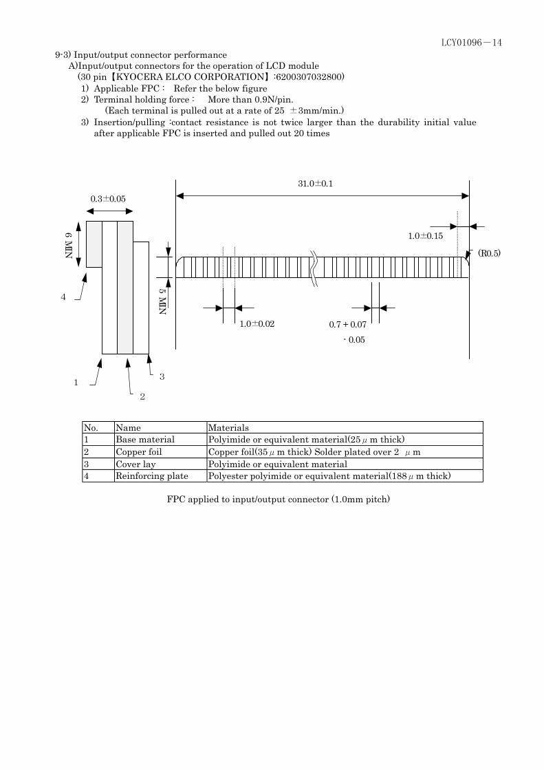
9-3) Input/output connector performance A)Input/output connectors for the operation of LCD module (30 pinޣKYOCERA ELCO CORPORATION6200307032800:ޤ)
1) Applicable FPC : Refer the below figure 2) Terminal holding force : More than 0.9N/pin.
(Each terminal is pulled out at a rate of 25 r3mm/min.) 3) Insertion/pulling :contact resistance is not twice larger than the durability initial value
after applicable FPC is inserted and pulled out 20 times
31.0r0.1 0.3r0.05
5 MIN
6 MIN
㧠
㧝 㧞
㧟
0.7 + 0.07 - 0.05
1.0r0.15
1.0r0.02
(R0.5)
No. Name Materials 1 Base material Polyimide or equivalent material(25Ǵm thick) 2 Copper foil Copper foil(35Ǵm thick) Solder plated over 2 Ǵm 3 Cover lay Polyimide or equivalent material 4 Reinforcing plate Polyester polyimide or equivalent material(188Ǵm thick)
FPC applied to input/output connector (1.0mm pitch)

LCY01096㧙15
(10) Display quality The display quality of the color TFT-LCD module shall be in compliance with the Incoming Inspection Standard.
(11) Mechanical Noise No abnormal mechanical noise which can be easily recognized when the module is shaken
by hand.
(12) Handling instructions 12-1) Mounting of module
The TFT-LCD module is designed to be mounted on equipment using the mounting tabs in the four corners of the module at the rear side. On mounting the module, as the M2.6 tapping screw fastening torque is 0.3 through 0.5N㨯m is recommended, be sure to fix the module on the same plane, taking care not to wrap or twist the module. Don't reach the pressure of touch-switches of the set side to a module directly, because images may be disturbed. Please power off the module when you connect the input/output connector.
12-2) Precautions in mounting
Polarizer which is made of soft material and susceptible to flaw must be handled carefully. Protective film (Laminator) is applied on the surface to protect it against scratches and dirts. It is recommended to peel off the laminator immediately before the use, taking care of static electricity. Precautions in peeling off the laminator
A) Working environment When the laminator is peeled off, static electricity may cause dust to stick to the polarizer surface. To avoid this, the following working environment is desirable. a) Floor : Conductive treatment of 1Mǡ or more on the tile. (conductive mat or
conductive paint on the tile) b) Clean room free form dust and with an adhensive mat on the doorway c) Advisable humidity:50%㨪70% Advisable temperature:15͠㨪27͠ d) Workers shall wear conductive shoes, conductive work clothes, conductive gloves
and an earth band. B) Working procedures
a) Direct the wind of discharging blower somewhat downward to ensure that module is blown sufficiently. Keep the distance between module and discharging blower within 20 cm.
b) Attach adhensive tape to the laminator part near discharging blower so as to protect polarizer against flaw.
c) Peel off laminator, pulling adhesive tape slowly to your side. d) On peeling off the laminator, pass the module to the next work process to prevent
the module to get dust.
discharging blower
less than 20cm m odule
D irection of w ind of blow er
Adhesive tape input connector
e) Method of removing dust from polarizer
• Blow off dust with N2 blower for which static electricity preventive measure has been taken. Ionized air gun (Hugle Electronics Co.) is recommended.
• Since polarizer is vulnerable, wiping should be avoided.

LCY01096㧙16
But when the panel has stain or grease, we recommend to use adhesive tape to softly remove them from the panel.
When metal part of the TFT-LCD module (shielding lid and rear case) is soiled, wipe it with soft dry cloth. For stubborn dirt, wipe the part, breathing on it. Wipe off water drop or finger grease immediately. Long contact with water may cause discoloration or spots. Since TFT-LCD module uses glass which breaks or cracks easily if dropped or bumped on hard surface, handle with care. Since CMOS LSI is used in this module, take care of static electricity and earth your body when handling.
12-3) Precautions in adjusting module Adjusting volumes on the rear face of the module have been set optimally before shipment. Therefore, do not change any adjusted values. If adjusted values are changed, the specifications described here may not be satisfied.
12-4) Caution of product design
The LCD module shall be protected against water salt-water by the waterproof cover. Please take measures to interferential radiation from module, to do not interfere surrounding appliances.
12-5)Mounting direction Mounting direction of the TFT-LCD module to the application needs to be carefully fixed by evaluating display performance.
12-6)Others
Do not expose the module to direct sunlight or intensive ultraviolet rays for many hours; liquid crystal is deteriorated by ultraviolet rays. Store the module at a temperature near the room temperature. At lower than the rated storage temperature, liquid crystal solidifies, causing the panel to be damaged. At higher than the rated storage temperature, liquid crystal turns into isotropic liquid and may not recover. The voltage of beginning electric discharge may over the normal voltage because of leakage current from approach conductor by to draw lump read lead line around. If LCD panel breaks, there may be a possibility that the liquid crystal escapes from the panel. Since the liquid crystal is injurious, do not put it into the eyes or mouth. When liquid crystal sticks to hands, feet or clothes, wash it out immediately with soap. Observe all other precautionary requirements in handling general electronic components.
(13) Shipping requirements
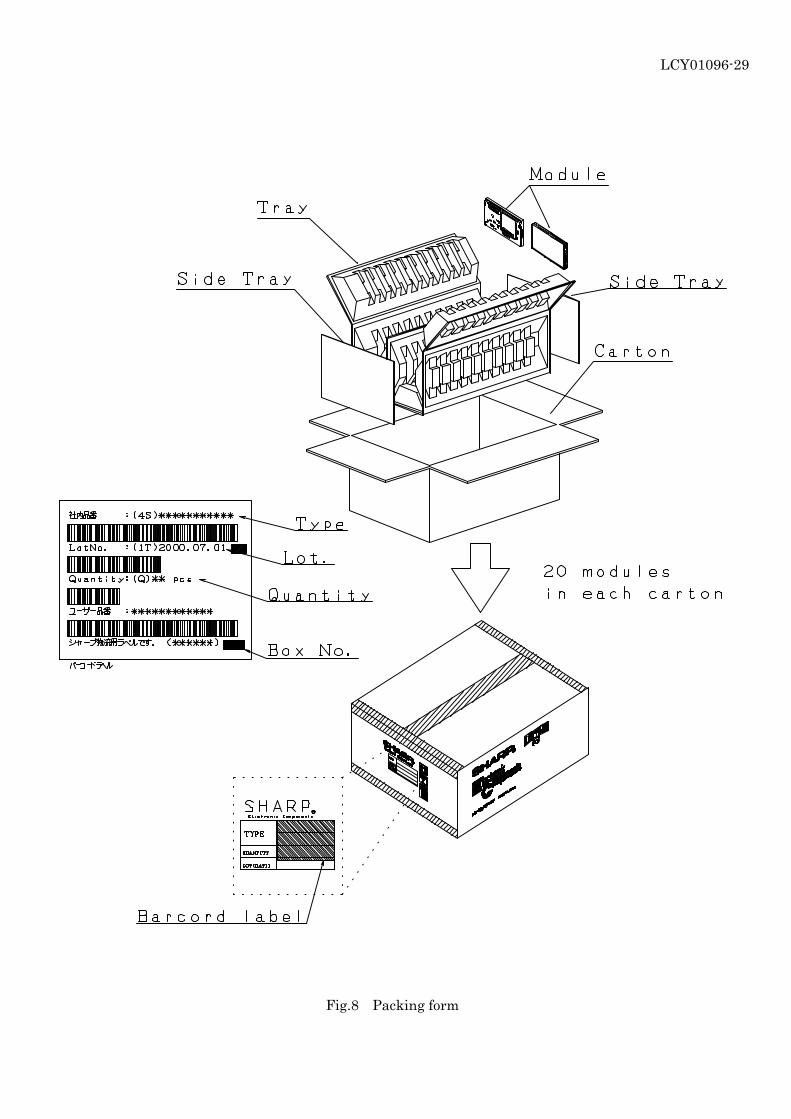
13-1) Packing form is shown in Fig.8. 13-2) Carton storage condition
Ԙ Number of layers of cartons in pile : 10 layers max. ԙ Environmental condition
㨯 Temperature 0͠ to 40͠ 㨯 Humidity 60 %PH or less (at 40͠) No dew condition even at a low temperature and high humidity 㨯 Atmosphere Harmful gases such as acid and alkali which corrode electronic components and wires must not be detected. 㨯 Storage period About 3 months 㨯 Opening of package To prevent TFT-LCD module from being damaged by static electricity, adjust the room humidity to 50%PH or higher and provide an appropriate measure for electrostatic earthing before opening the package.

LCY01096㧙17
(14)Reliability test conditions Reliability test conditions for the TFT-LCD module are shown in Table 10. (15)Others 15-1)Indication of lot number The lot number is shown on a label. Attached location is shown in Fig.1(Outline Dimensions). Indicated contents of the label
LQ065T5AR01 ٤٤٤٤٤٤٤٤٤٤ model No. lot No. Contents of lot No. the 1st figure ̕ production year (ex.1999 : 9) the 2nd figure ̕ production month 1,2,3,̖̖,9,X,Y,Z the 3rd~8th figure ̕ serial No. 00001㨪 the 9th figure ̕ revision marks blank or A,B,C ̖ the 10th figure ̕ production factory code blank or A,B,C ̖

LCY01096㧙18
Reliability test conditions for TFT-LCD module Table 10
Remark) Temperature condition is based on operating temperature conditions on (6)-Table 5
No. Test items Test conditions 1
High temperature storage test
Ta=+85͠ 240h
2
Low temperature storage test
Ta=-40͠ 240h
3
High temperature And high humidity operating test
Ta=+60͠, 90%RH 240h
4
High temperature operating test
Tp=+85͠㧔Ta=+65͠㧕 240h
5
Low temperature operating test
Ta=-30͠ 240h
6
Electro static discharge test
r200V, 200pF(0ǡ) 1 times for each terminals
7
Shock test
980m/s㧞㨯6ms, rX, rY, rZ 3times for each direction (JIS C0041,A-7 condition C)
8
Vibration test
Frequency range : 8㨪33.3Hz Stroke : 1.3mm Sweep : 33.3Hz㨪400Hz Acceleration : 28.4 m/s㧞 Cycle : 15 minutes X,Z 2 hours for each directions, 4 hours for Y direction (total 8 hours) ޣcautionޤ (JIS D1601)
9
Heat shock test storage test
Ta=-30㨪+85͠ / 200cycles (0.5h) (0.5h)
Ta=Ambient temperature, Tp=Panel temperatureޤNoteޣ In the standard condition, there shall be no practical problems that may affectޤCheck itemsޣ the display function. X,Y,Z directions are shown as followsޤCautionޣ
䌘 䌙
䌚

LCY01096-19
Fig.1 Outline dimensions of TFT-LCD module

.
Fig.2 Circuit block diagram of the module
Gate driver
Source driver
䌔䌆䌔䋭䌌䌃䌄
Power supply circuit
Control circuit
Video interface circuit Common
electrode driving signal circuit
Backlight Backlight driving circuit
Gate driver driving signal
Source driver driving signal
䋯䋯䋯
Common electrode driving signal
LCD driving signal
11112222 VINVINVINVIN
㧞㧞㧞㧞 CLKCCLKCCLKCCLKC
23232323 CLKCLKCLKCLK----
㧟㧟㧟㧟 HSYHSYHSYHSY
㧠㧠㧠㧠 VSYVSYVSYVSY
㧢㧢㧢㧢 NTPNTPNTPNTP
25252525 VSWVSWVSWVSW
13131313 VBSVBSVBSVBS
17171717 16161616 15151515 VR1,VG1,VB1VR1,VG1,VB1VR1,VG1,VB1VR1,VG1,VB1
21212121 20202020 11119999 VR2,VG2,VB2VR2,VG2,VB2VR2,VG2,VB2VR2,VG2,VB2
VBLVBLVBLVBL 28282828 27272727
24242424 CLK+CLK+CLK+CLK+
26262626 PWMIPWMIPWMIPWMI
㧡㧡㧡㧡 PWMSPWMSPWMSPWMS
11111111 11110000 㧥㧥㧥㧥 MODSMODSMODSMODS,MODW,,MODW,,MODW,,MODW,MODNMODNMODNMODN
14141414 BRTBRTBRTBRT
㧤㧤㧤㧤 VRVVRVVRVVRV
㧣㧣㧣㧣 HRVHRVHRVHRV
䋯䋯䋯
Backlight driving signal
+8.0V
+8.0V
LC
Y01096
䋭20
LVDS Receiver


䌖䌂䌓 䌖䌓䌙 VIDEO
(R,G,B㧕 䌈䌓䌙
Fig.4㧙A Input / Output signal waveforms(CLKC=̍Hi̍)
3䌈(NTSC)
16.7ms(NTSC) odd field even field
1.0Vp-p
LCY01096-22
2.5䌈(PAL)
20.0ms(PAL)
㱠pv1 㱠pv2
㱠VS
0.7Vp-p
㱠fvo
㱠VHO
㱠fHO 㱠rHO
㱠VHO
㱠rVO
Vertically display period
detailed
VSY
HSY

Fig.4㧙B Input/Output signal waveforms (CLKC=̍Hi̍)
LCY01096-23
50%
90%
10%
㱠fHO 㱠rHO 㱠HS2
�H=63.5㱘s(NTSC)
�H=64.0㱘s(PAL)
㱠pd
㱠HS1
Horizontally display area
VBS
HSY
Video signal
VR�㨪VB� or
VR2㨪VB2

㧴 㧿 㨅㧴 㧿 㨅㧴 㧿 㨅㧴 㧿 㨅
C L K +C L K +C L K +C L K + C L KC L KC L KC L K 㧙㧙㧙㧙
㧴㧿㨅㧴㧿㨅㧴㧿㨅㧴㧿㨅
tSU1 tHO 1
Ǽ fHI2 Ǽ rHI2 Ǽ HI
㧴㧿㨅㧴㧿㨅㧴㧿㨅㧴㧿㨅
㨂㧿㨅㨂㧿㨅㨂㧿㨅㨂㧿㨅
1H
Ǽ rVO
tSU2
㨂㧿㨅㨂㧿㨅㨂㧿㨅㨂㧿㨅
㧴㧿㨅㧴㧿㨅㧴㧿㨅㧴㧿㨅
tH02
Ǽ fVO
Fig. 4㧙C Input/Output signal waveforms (external clock mode NTP=”Hi”, CLKC=”Lo”)
LCY01096���

P W MP W MP W MP W M SSSS ( N T S C )( N T S C )( N T S C )( N T S C )
P W MP W MP W MP W M SSSS ( P A L )( P A L )( P A L )( P A L )
P W MP W MP W MP W M SSSS
V S YV S YV S YV S Y
H S YH S YH S YH S Y
㨂 㧿 㨅㨂 㧿 㨅㨂 㧿 㨅㨂 㧿 㨅
䋶 䋲 䋵 䌈 䋨 䌐 䌁 䌌 䋩
䋵 䋲 䋵 䌈 䋨 䌎 䌔 䌓 䌃 䋩
䋸 䋹 䌈
䋱 䋰 䋵 䌈
䋶 䋲 䋵 䌈 䋨 䌐 䌁 䌌 䋩
䋵 䋲 䋵 䌈 䋨 䌎 䌔 䌓 䌃 䋩
䌮 䌈
䌮 䌈
䋱 䌈
䋱 䋯 䋲 䌈 䋱 䋯 䋲 䌈
䋸 䋹 䌈
䋱 䋰 䋵 䌈
i n v e r t e r o s c i l l a t i o n n o i n v e r t e r o s c i l l a t i o n
m a g n i f y t i m e r a n g e
䋱 䋯 䋲 䌈 䋱 䋯 䋲 䌈
P W MP W MP W MP W M IIII
Fig. 4-D PWM dimming timing
.%;���������

LCY01096㧙26
Photodetector
(including luminosity factor)
Center
TFT-LCD module LCD panel
Fig. 5 Measuring method of optical characteristics

LCY01096㧙27
ޤReferenceޣClock and Video signal timing [Input Condition]
DotClock frequency 㨒CLK = 8.0MHz Hsyn. frequency fH㧩15.748kHz Vsyn. Frequency fV㧩60.107Hz Video Signal Cross-Hatching
(To show white lines every 24 dots with the background display of Balck) Amplitude = 0.7Vpp TVr㧩TVf㧩17ns TVH㧩125ns
Fig.6 Clock and Video signal timing
φ black level
CLK -
Input Video 0.7Vpp
CLK +
φ white level
TVH㧩㧩㧩㧩125ns
TVr TVf
㨠㨠㨠㨠d
White Vertical Line

LCY01096-28
Fig.7 Construction of TFT-LCD module
LCY01096-29
Fig.8 Packing form

SPECIFICATIONS ARE SUBJECT TO CHANGE WITHOUT NOTICE.Suggested applications (if any) are for standard use; See Important Restrictions for limitations on special applications. See Limited �Warranty for SHARP’s product warranty. The Limited Warranty is in lieu, and exclusive of, all other warranties, express or implied. �ALL EXPRESS AND IMPLIED WARRANTIES, INCLUDING THE WARRANTIES OF MERCHANTABILITY, FITNESS FOR USE AND �FITNESS FOR A PARTICULAR PURPOSE, ARE SPECIFICALLY EXCLUDED. In no event will SHARP be liable, or in any way responsible,�for any incidental or consequential economic or property damage.
NORTH AMERICA EUROPE JAPAN
SHARP Microelectronics of the Americas5700 NW Pacific Rim Blvd.Camas, WA 98607, U.S.A.Phone: (1) 360-834-2500Fax: (1) 360-834-8903Fast Info: (1) 800-833-9437www.sharpsma.com
SHARP Microelectronics EuropeDivision of Sharp Electronics (Europe) GmbHSonninstrasse 320097 Hamburg, GermanyPhone: (49) 40-2376-2286Fax: (49) 40-2376-2232www.sharpsme.com
SHARP CorporationElectronic Components & Devices22-22 Nagaike-cho, Abeno-KuOsaka 545-8522, JapanPhone: (81) 6-6621-1221Fax: (81) 6117-725300/6117-725301www.sharp-world.com
TAIWAN SINGAPORE KOREA
SHARP Electronic Components(Taiwan) Corporation8F-A, No. 16, Sec. 4, Nanking E. Rd.Taipei, Taiwan, Republic of ChinaPhone: (886) 2-2577-7341Fax: (886) 2-2577-7326/2-2577-7328
SHARP Electronics (Singapore) PTE., Ltd.438A, Alexandra Road, #05-01/02Alexandra Technopark, Singapore 119967Phone: (65) 271-3566Fax: (65) 271-3855
SHARP Electronic Components(Korea) CorporationRM 501 Geosung B/D, 541Dohwa-dong, Mapo-kuSeoul 121-701, KoreaPhone: (82) 2-711-5813 ~ 8Fax: (82) 2-711-5819
CHINA HONG KONG
SHARP Microelectronics of China(Shanghai) Co., Ltd.28 Xin Jin Qiao Road King Tower 16FPudong Shanghai, 201206 P.R. ChinaPhone: (86) 21-5854-7710/21-5834-6056Fax: (86) 21-5854-4340/21-5834-6057Head Office:No. 360, Bashen Road, Xin Development Bldg. 22Waigaoqiao Free Trade Zone Shanghai200131 P.R. ChinaEmail: [email protected]
SHARP-ROXY (Hong Kong) Ltd.3rd Business Division,17/F, Admiralty Centre, Tower 118 Harcourt Road, Hong KongPhone: (852) 28229311Fax: (852) 28660779www.sharp.com.hkShenzhen Representative Office:Room 13B1, Tower C,Electronics Science & Technology BuildingShen Nan Zhong RoadShenzhen, P.R. ChinaPhone: (86) 755-3273731Fax: (86) 755-3273735