LCD Color Television - Cjoint.com · LCD Color Television 40LV733G Ver. 2.00 ... Run the program...
66
SERVICE MANUAL LCD Color Television 40LV733G Ver. 2.00 This model is classified as a green product (*1), as indicated by the underlined serial number. This Service Manual describes replacement parts for the green product. When repairing this green product, use the part(s) described in this manual and lead-free solder (*2). For (*1) and (*2), refer to GREEN PRODUCT PROCUREMENT and LEAD-FREE SOLDER. © TOSHIBA CORPORATION
Transcript of LCD Color Television - Cjoint.com · LCD Color Television 40LV733G Ver. 2.00 ... Run the program...
SERVICE MANUAL
LCD Color Television
40LV733G Ver. 2.00
This model is classified as a green product (*1), as indicated by the underlined serial number.
This Service Manual describes replacement parts for the green product. When repairing this
green product, use the part(s) described in this manual and lead-free solder (*2).
For (*1) and (*2), refer to GREEN PRODUCT PROCUREMENT and LEAD-FREE
SOLDER.
© TOSHIBA CORPORATION
IMPORTANT NOTICE
WARNING:
You are requested that you shall not modify or alter the information or data
provided herein without prior written consent by Toshiba. Toshiba shall not
be liable to anybody for any damages, losses, expenses or costs, if any,
incurred in connection with or as a result of such modification or alteration.
THE INFORMATION OR DATA HEREIN SHALL BE PROVIDED "AS IS"
WITHOUT ANY WARRANTY OF ANY KIND, EITHER EXPRESS OR IMPLIED
WARRANTY OF MERCHANTABILITY AND FITNESS FOR A PARTICULAR
PURPOSE.
Toshiba shall not be liable for any damages, losses, expenses or costs, if
any, incurred in connection with or as a result of use of any information or
data provided herein.
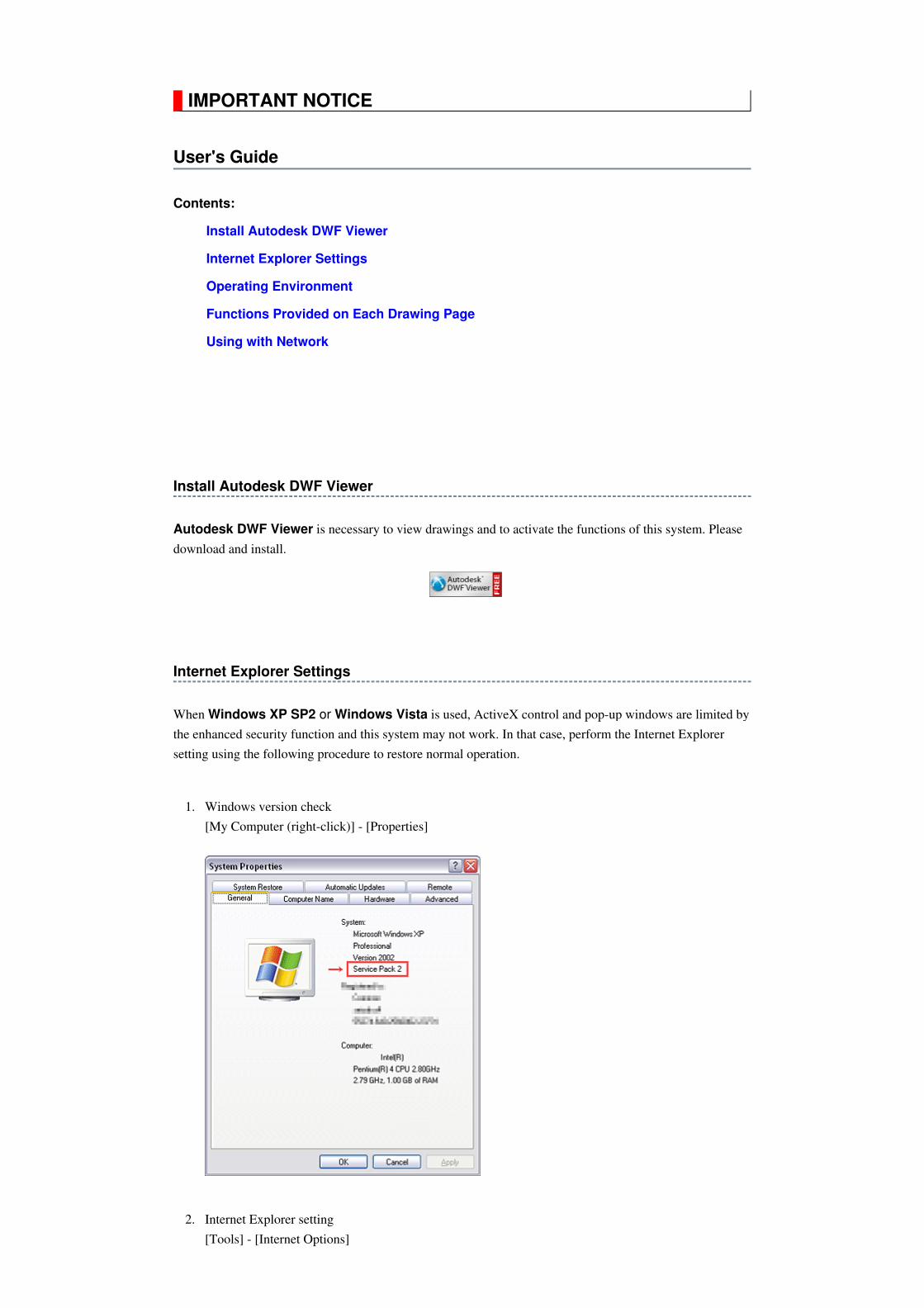
IMPORTANT NOTICE
User's Guide
Contents:
Install Autodesk DWF Viewer
Internet Explorer Settings
Operating Environment
Functions Provided on Each Drawing Page
Using with Network
Install Autodesk DWF Viewer
Autodesk DWF Viewer is necessary to view drawings and to activate the functions of this system. Please
download and install.
Internet Explorer Settings
When Windows XP SP2 or Windows Vista is used, ActiveX control and pop-up windows are limited by
the enhanced security function and this system may not work. In that case, perform the Internet Explorer
setting using the following procedure to restore normal operation.
1. Windows version check
[My Computer (right-click)] - [Properties]
2. Internet Explorer setting
[Tools] - [Internet Options]
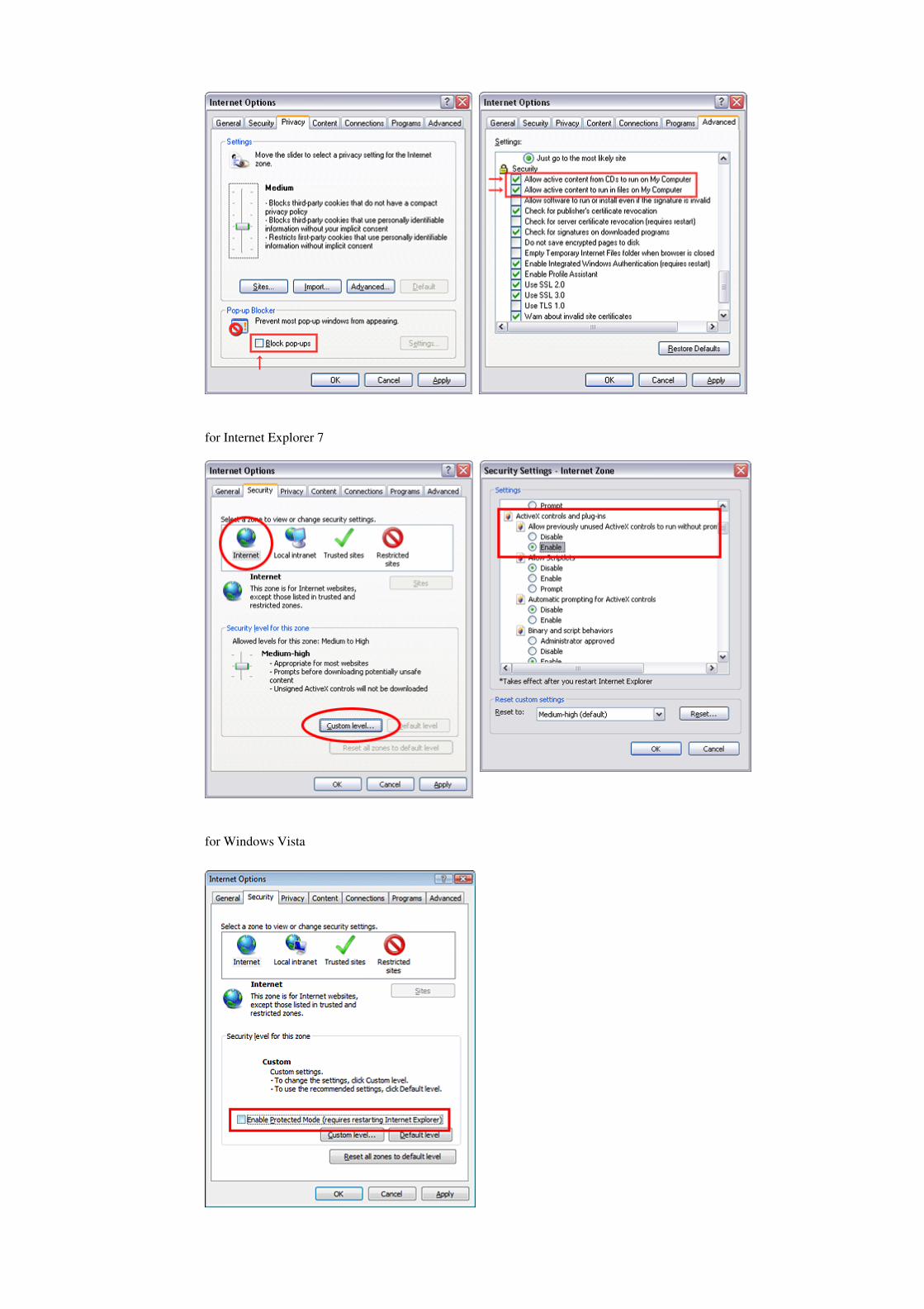
for Internet Explorer 7
for Windows Vista
Operating Environment
Functions Provided on Each Drawing Page
Parts Information Reference Function
When the character string of a part on the drawing is clicked, its information is popped up at the location.
You can get any parts information immediately on the screen without referring to the maintenance parts list.
Parts Search Function
You can search any part within the displayed drawing or within the whole schematic diagram/board view by
specifying a location number. The pop-up window displayed by clicking a part 's character string allows to
search the part within the applicable schematic diagram, board view or spare parts list.
A circle appears when the part is found, showing the part's location within the drawing.
Signal Line/Connector Destination Display Function
When a name at the end of a signal line in a divided schematic diagram is clicked, the destination of the
signal is searched and the display changes to the destination. Connecter destinations can also be searched in
the same way.
When two or more search results are provided, their drawing names are displayed, allowing you to choose a
desired drawing to display.
Layer Display Changing Function
When any of the color buttons on the toolbar is clicked, it can be selected to display desired layer in its color
or not to display each layer. This allows you to see the pattern layer only by setting other layers to "non-
display".
PC Board View Pattern Highlighting Function
When a pattern on a board view is clicked, it is highlighted in green. This allows easy pattern tracing.
Specified Area Printing Function
The Autodesk DWF Viewer enables to print the displayed drawing region as it is on a printer. It also allows
to print a large-sized drawing in multiple pieces (tile printing).
Using with Network
PRECAUTION
To use ZEUS Service Manual Ver.2 with network, the file-path names written on the source files of each
PC : Pentium III or higher recommended
Monitor : 1024 x 768 or higher resolution recommended
Mouse : A mouse with wheel recommended
OS : Microsoft Windows 2000 SP4 / XP / Vista
Browser : Microsoft Internet Explorer 6.0 / 7.0
Drawing viewer : Autodesk DWF Viewer 6.0 / 7.0
* Use the software following respective license terms and conditions.
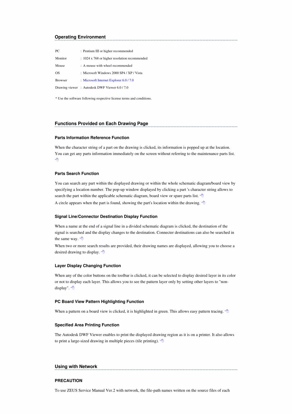
ZEUS Engine Program Ver.2 and ZEUS Service Manual Ver.2 are to be modified.
Perform the procedure described below.
Preparation
1. Run the program file zuesFPch.exe to install the program file for File-Path to the Local PC.
-> Download zeusFPch_setup.zip (2.3MB)
2. Run the program file ZeusSetup_v2.0.exe to install the ZEUS Engine Program in C:\Program
Files\zeus of the local PC. This can be done by running the installer program provided.
3. Create the appropriate folder where the ZEUS Engine Program Ver.2 and the ZEUS Service Manual
Ver.2 to be stored in the server.
4. Move the ZEUS Engine Program of step 2 to the folder created at step 3 in the Server.
5. Detach the ZEUS Service Manual Ver.2 to the folder created at step 3 in the Server.
6. Unzip the ZEUS Service Manual Ver.2 within the folder in the Server.
Example of folder
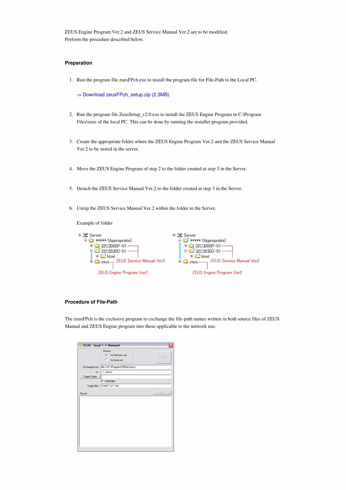
Procedure of File-Path
The zeusFPch is the exclusive program to exchange the file-path names written in both source files of ZEUS
Manual and ZEUS Engine program into those applicable to the network use.
1. Whenever changing the file-path of both ZEUS Engine Program and ZEUS Service Manual to use with
network, pay the attention to set the "Exchange to" column that should have a proper relation between
ZEUS Engine Program and ZEUS Service Manual with referring the following.
Run the zeusFPch and set "Exchange to" by referring to the examples below.
Example 1 :
In the "Exchange to" column shows the relation between ZEUS Service Manual and ZEUS Engine
Program.
../ counts the relation between.
Thus in this case, it must be ../../zeus/ (2 counts).
Example 2 :
In this case, it must be ../../../zeus/ (3 counts).
2. Run the zeusFPch to change the path in the ZEUS Engine Program Ver.2.
3. Set ZEUS Engine Program in the created folder in the server to the "Target Folder", and then press
"START".
(This procedure is one time only)
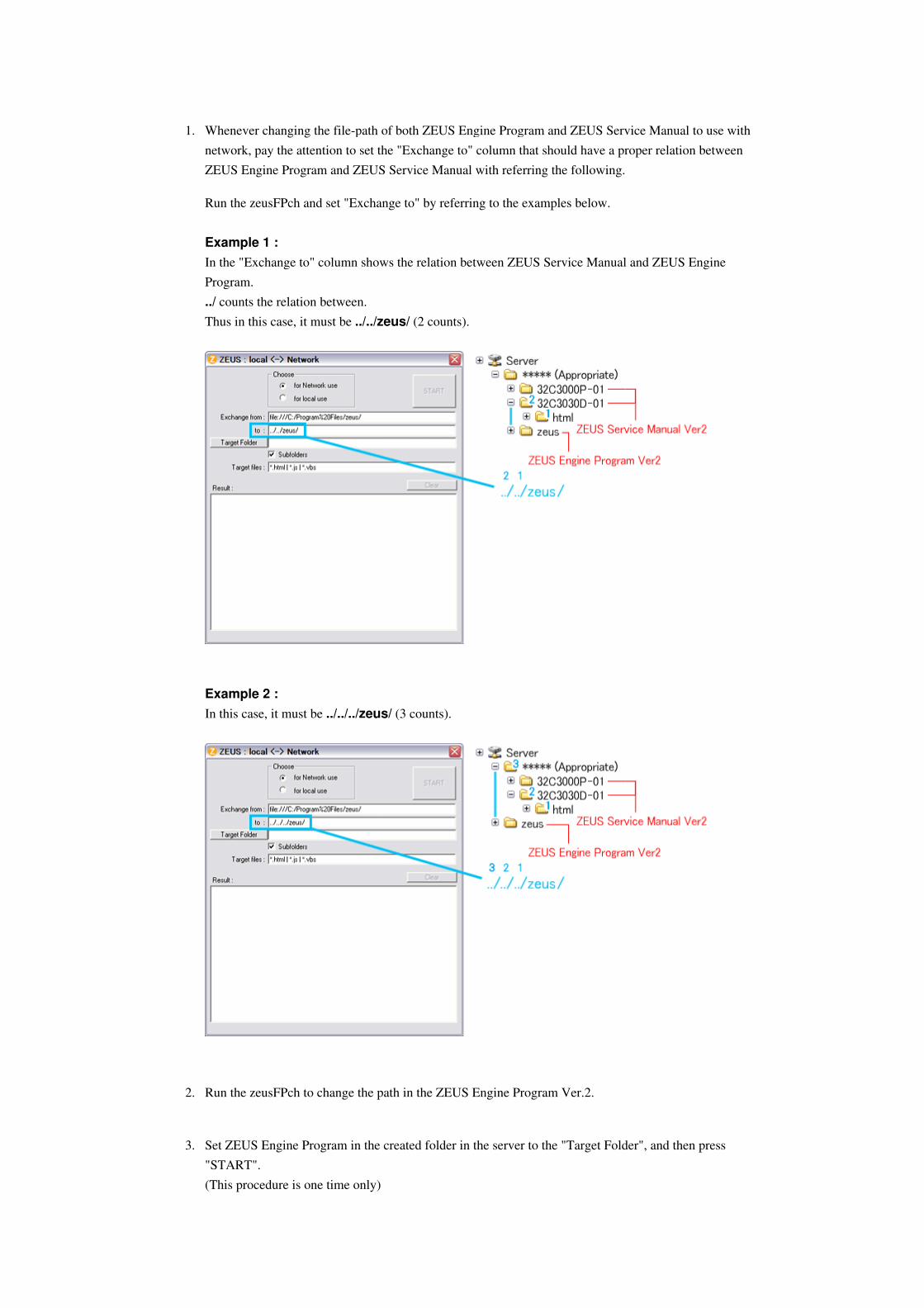
4. Run the ZeusFPch to change the path in the ZEUS Service Manual Ver2.
5. Set unzipped ZEUS Service Manual in the created folder in the server to the "Target Folder", and then
press "START".
(This procedure is required whenever placing service manual.)
Confirmation
Confirm that service manual on the server can be operated normally by client PC.
Note:
In case of accessing the ZEUS Manual through WEB site, the small pop-up window appears at the left
bottom corner on the screen whenever searching the location links. This is not malfunction.
IMPORTANT NOTICE
A Known Malfunction
Autodesk® DWF™ Viewer version (Free software provided through WEB)
Use Autodesk DWF Viewer ver. 6.0.
Through WEB, ver. 6.5 has been released but with it, the linking function in this manual may
not work properly.
If ver. 6.5 has been installed, uninstall it and reinstall ver. 6.0.
To get ver. 6.0, click the icon, or contact to the nearest Toshiba Service Centre for further
assistance.
Freezing windows opened (Cannot close the open windows)
This may happen occasionally.
In case of encountering this, follow the procedure below.
1. Press [Ctrl], [Alt] and [Delete] keys at the same time to engage windows security
windows.
2. Then, choose TASK manager and Application tab, and select TOSHIBA SERVICE
MANUAL-Microsoft Internet Explorer.
3. Click TASK-end.
Main Window back forwarded
The real cause has not been found yet but with this condition, nothing disturbs the service
manual operation.
Continue to use by operating the windows.
Precaution when opening the diagrams
While opening the diagrams, the menu in the left frame changes its color to GRAY. This is
an indication that the viewer is processing.
With this condition, the menu indication color may stick to the GRAY color or Windows
may freeze if clicking other menu.
To avoid such things, do not operate any others while menu turns GRAY color.
If entering this, re-open the service manual or refresh the left frame.

GREEN PRODUCT PROCUREMENT
The EC is actively promoting the WEEE & RoHS Directives that define standards for
recycling and reuse of Waste Electrical and Electronic Equipment and for the Restriction of
the use of certain Hazardous Substances. From July 1, 2006, the RoHS Directive will
prohibit any marketing of new products containing the restricted substances.
Increasing attention is given to issues related to the global environmental. Toshiba
Corporation recognizes environmental protection as a key management tasks, and is doing its
utmost to enhance and improve the quality and scope of its environmental activities. In line
with this, Toshiba proactively promotes Green Procurement, and seeks to purchase and use
products, parts and materials that have low environmental impacts.
Green procurement of parts is not only confined to manufacture. The same green parts used
in manufacture must also be used as replacement parts.

LEAD-FREE SOLDER
This product is manufactured using lead-free solder as a part of a movement within the
consumer products industry at large to be environmentally responsible. Lead-free solder must
be used in the servicing and repair of this product.
The melting temperature of lead-free solder is higher than that of leaded solder by 86ºF to
104ºF (30ºC to 40ºC). Use of a soldering iron designed for lead-based solders to repair
product made with lead-free solder may result in damage to the component and or PCB being
soldered. Great care should be made to ensure high-quality soldering when servicing this
product especially when soldering large components, through-hole pins, and on PCBs as the
level of heat required to melt lead-free solder is high.
WARNING: This product is manufactured using lead free solder.
DO NOT USE LEAD BASED SOLDER TO REPAIR THIS PRODUCT!
SAFETY INSTRUCTION
Safety Precaution
1. An isolation transformer should be connected in the power line between the receiver
and the AC line before any service is performed on the receiver.
2. Always disconnect the power plug before any disassembling of the product. It may
result in electrical shock.
3. When replacing a chassis in the cabinet, always be certain that all the protective
devices are put back in place, such as nonmetallic control knobs, insulating covers,
shields, isolation resistor-capacitor network, etc.
4. Always keep tools, components of the product, etc away from the children, These items
may cause injury to children.
5. Depending on the model, use an isolation transformer or wear suitable gloves when
servicing with the power on, and disconnect the power plug to avoid electrical shock
when replacing parts. In some cases, alternating current is also impressed in the
chassis, so electrical shock is possible if the chassis is contacted with the power on.
6. Always use the replacement parts specified for the particular model when making
repairs. The parts used in products require special safety characteristics such as
inflammability, voltage resistance, etc. therefore, use only replacement parts that have
these same characteristics. Use only the specified parts when the mark is indicated
in the circuit diagram or parts list.
7. Parts mounting and routing dressing of wirings should be the same as that used
originally. For safety purposes, insulating materials such as isolation tube or tape are
sometimes used and printed circuit boards are sometimes mounted floating. Also make
sure that wirings is routed and clamped to avoid parts that generate heat and which use
high voltage. Always follow the manufactured wiring routes / dressings.
8. Always ensure that all internal wirings are in accordance before re-assembling the
external casing after a repairing completed. Do not allow internal wiring to be pinched
by cabinets, panels, etc. Any error in reassembly or wiring can result in electrical
leakage, flame, etc., and may be hazardous.
9. NEVER remodel the product in any way. Remodeling can result in improper operation,
malfunction, or electrical leakage and flame, which may be hazardous.
WARNING: BEFORE SERVICING THIS CHASSIS, READ THE "SAFETY
PRECAUTION" AND "PRODUCT SAFETY NOTICE" INSTRUCTIONS BELOW.
WARNING: SERVICING SHOULD NOT BE ATTEMPTED BY ANYONE
UNFAMILIAR WITH THE NECESSARY PRECAUTIONS ON THIS RECEIVER.
THE FOLLOWING ARE THE NECESSARY PRECAUTIONS TO BE OBSERVED
BEFORE SERVICING THIS CHASSIS.

10. Touch current check. (After completing the work, measure touch current to prevent an
electric shock.)
Plug the AC cord directly into the AC outlet. Do NOT use an isolation transformer
for this check.
Connect a measuring network for touch currents between each exposed metallic part
on the set and a good earth ground such as a water pipe.
The potential at any point (TOUCH CURRENT) expressed as voltage and
does not exceed the following value:
Product Safety Notice
Many electrical and mechanical parts in this chassis have special safety-related
Annex D
(normative)
Measuring network for TOUCH CURRENTS
Resistance values in orms (Ω).
Input resistance : 1 MΩ Input capacitance : 200 pF
Frequency range : 15 Hz to 1 MHz and d.c. respectively
Note: Appropriate measures should be taken to obtain the correct value in case of non
sinusoidal waveforms.
The measuring instrument is calibrated by comparing the frequency factor of with the
solid line in figure F.2 of IEC 60990 at various frequencies. A calibration curve is
constructed showing the deviation of from the ideal curve as a function of frequency.
TOUCH CURRENT = /500 (peak value).
V: Voltmeter or oscilloscope
(r.m.s. or peak reading)
The part or contact of a TERMINAL is not HAZARDOUS LIVE if:
Note: The limit values of = 0.35 V (peak) for a.c. and = 1.0 V for d.c. correspond to
the values 0.7 mA (peak) a.c. and 2.0 mA d.c.
a) The open-circuit voltage should not exceed 35 V (peak) a.c. or 60 V d.c. or, if a) is not
met.
b) The measurement of the TOUCH CURRENT shall be carried out in accordance with
IEC 60990, with the measuring network described in Annex D of this standard.
The TOUCH CURRENT expressed as voltages and , does not exceed the
following values:
- for a.c. : = 35 V (peak) and = 0.35 V (peak); - for d.c. : = 1.0 V

characteristics. These characteristics are often passed unnoticed by a visual inspection and
the protection afforded by them cannot necessarily be obtained by using replacement
components rated for higher voltage, wattage, etc. Replacement parts which have these
special safety characteristics are identified in this manual and its supplements; electrical
components having such features are identified by the international hazard symbols on the
schematic diagram and the parts list.
Before replacing any of these components, read the parts list in this manual carefully. The
use of substitute replacement parts which do not have the same safety characteristics as
specified in the parts list may create electrical shock, fire, or other hazards.
SAFETY INSTRUCTION
Handling the LCD Module
Safety Precaution
In the event that the screen is damaged or the liquid crystal (fluid) leaks, do not breathe in or
drink this fluid.
Also, never touch this fluid. Such actions could cause toxicity or skin irritation. If this fluid
should enter the mouth, rinse the mouth thoroughly with water. If the fluid should contact the
skin or clothing, wipe off with alcohol, etc., and rinse thoroughly with water. If the fluid
should enter the eyes, immediately rinse the eyes thoroughly with running water.
Precautions for Handling the LCD Module
The LCD module can easily be damaged during disassembly or reassembly; therefore,
always observe the following precautions when handling the module.
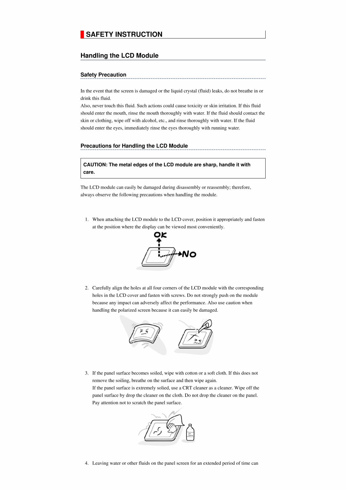
1. When attaching the LCD module to the LCD cover, position it appropriately and fasten
at the position where the display can be viewed most conveniently.
2. Carefully align the holes at all four corners of the LCD module with the corresponding
holes in the LCD cover and fasten with screws. Do not strongly push on the module
because any impact can adversely affect the performance. Also use caution when
handling the polarized screen because it can easily be damaged.
3. If the panel surface becomes soiled, wipe with cotton or a soft cloth. If this does not
remove the soiling, breathe on the surface and then wipe again.
If the panel surface is extremely solied, use a CRT cleaner as a cleaner. Wipe off the
panel surface by drop the cleaner on the cloth. Do not drop the cleaner on the panel.
Pay attention not to scratch the panel surface.
4. Leaving water or other fluids on the panel screen for an extended period of time can
CAUTION: The metal edges of the LCD module are sharp, handle it with
care.
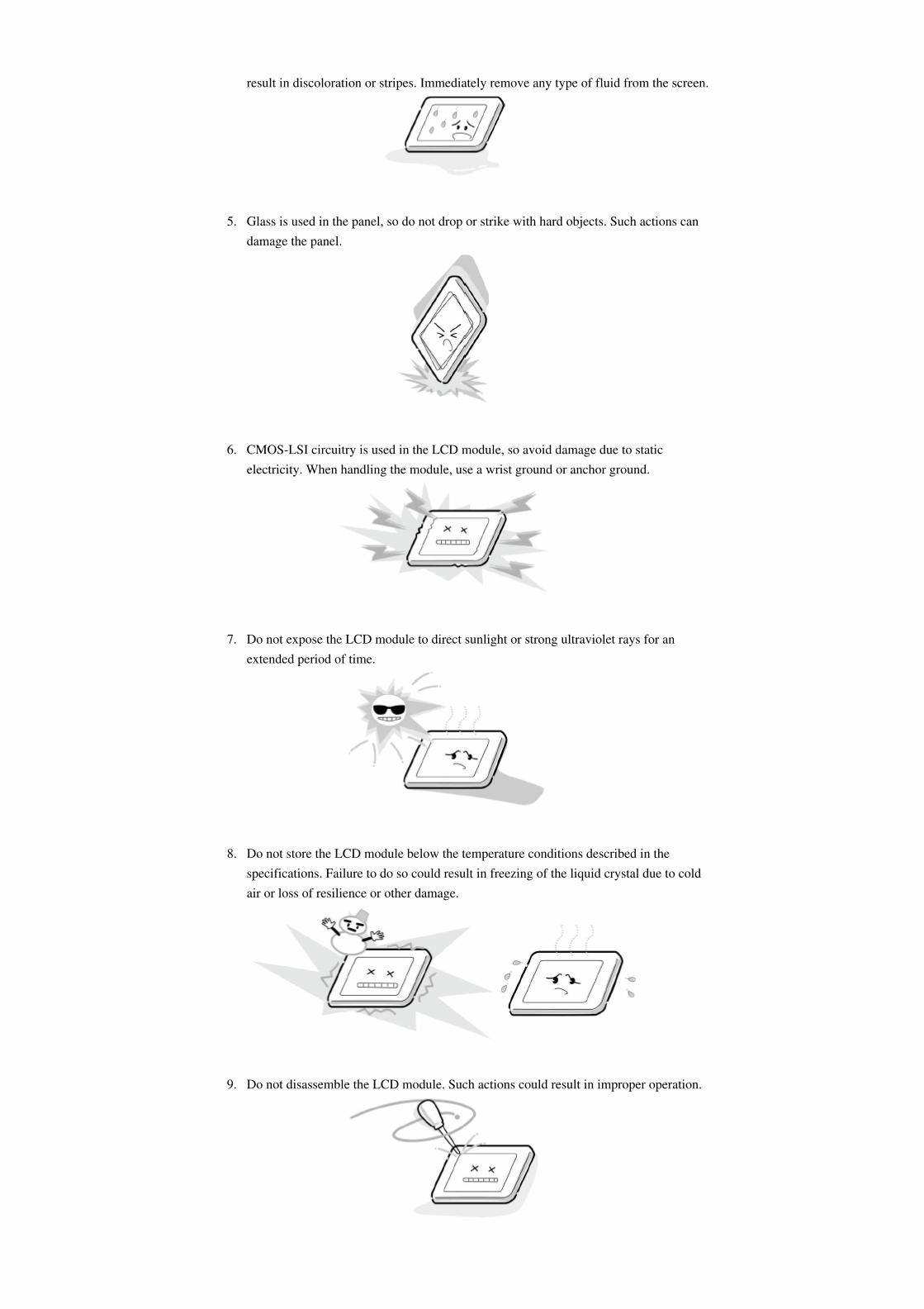
result in discoloration or stripes. Immediately remove any type of fluid from the screen.
5. Glass is used in the panel, so do not drop or strike with hard objects. Such actions can
damage the panel.
6. CMOS-LSI circuitry is used in the LCD module, so avoid damage due to static
electricity. When handling the module, use a wrist ground or anchor ground.
7. Do not expose the LCD module to direct sunlight or strong ultraviolet rays for an
extended period of time.
8. Do not store the LCD module below the temperature conditions described in the
specifications. Failure to do so could result in freezing of the liquid crystal due to cold
air or loss of resilience or other damage.
9. Do not disassemble the LCD module. Such actions could result in improper operation.

10. When transporting the LCD module, do not use packing containing epoxy resin
(amine) or silicon resin (alcohol or oxim). The gas generated by these materials can
cause loss of polarity.
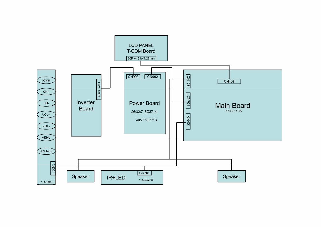
LCD PANEL
T-COM Board
30P or 51p/1.25mm
power 14
P/
CN903 CN902
CN408
CN
128
Main BoardPower BoardInverter
Board
CH+
CH-
/2.0
mm C
N701
715G370526/32:715G3714VOL+
VOL-
MENU
CN
401
40:715G3713
SOURCE
CCN
00
1
Speaker IR+LED SpeakerCN201
715G3945715G3730
To Panel
U401
SCALER
MT5363
BGA522
CVBS
HDMI3
HDMI1
U602
Sound AMP
BD5444EFV
SCART1/2 Audio
Component Audio
VGA/HDMI Audio
Side AV Audio
USB
HDMI2
SCART1
Component
Side I/O
VGA SCART1
Audio OUT
PCMCIADATA/ADDR
U402
EEPROM
M24C02
SCART2
VDAC_Out2
Half In/Monitor out
Full In/TV out
IFS P/N
CVBS2
IF P/N TV
TS In
SCART2
Audio OUT
U128
HDMI SW
SiI9187
26"
32"/37"/42"10W / 6Ohm
5W / 8Ohm
26"/32" WXGA
37"/40" FHD
USB P/M
Rx InTx 0-2, Txc
SPK_Out_L/R
Head Phone
Side I/O
KEYPAD
IR
LED
KEYPAD/IR
BOARD
SPDIF Optical
I/O 0_7
SY0/SC0
16MB NAND Flash
U405
YPbPr0
RGB/HV
SY1/SC1
CVBS3
DDR2
32MB x 16
U402/U403
ASPDIF
OSCL0
OSDA0
ORESET#
EEPROM
M24C32
U609
U410
Reset
MAX809ST
IFT P/NTU101
Tuner
ENV57S01D8FIFC P/N
TS Out
U606
HP AMP
TPA6132
U605
Line Driver
DRV602
HP_Out_L/R HP_Out_LT/RT
U604
Line Driver
DRV602
SCART1_Out_L/R
SCART2_Out_L/R
SCART1 L/R
SCART2 L/R
VDAC_Out2
YPbPr1
AIN3/4
AIN0/1
AIN2
AIN6
AIN5
AL1
AR1
AL0
AR0
AL2
AR2
AL3
AR3
TS INU610
DVB-C
Si2163
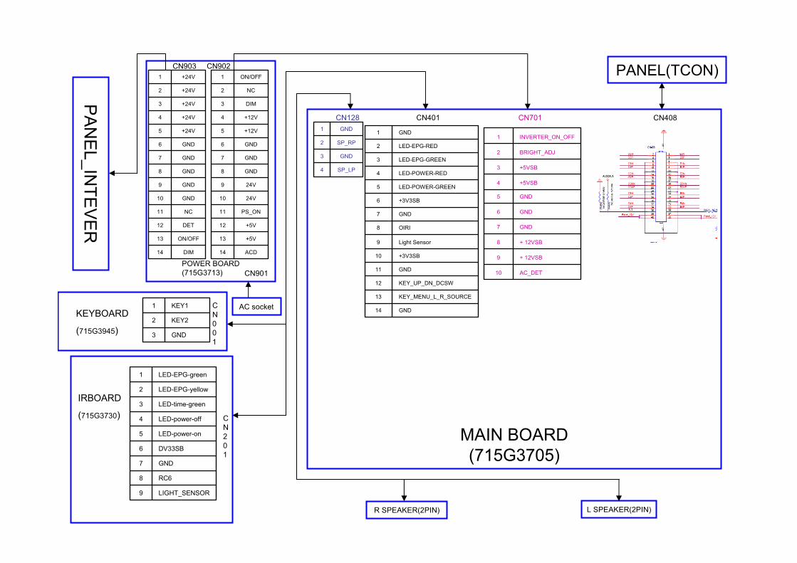
MAIN BOARD
(715G3705)
POWER BOARD
(715G3713)
PA
NE
L_IN
TE
VE
R
CN902
CN701CN401CN128
L SPEAKER(2PIN)R SPEAKER(2PIN)
CN408
PANEL(TCON)
PS_ON11
+5V12
+5V13
ACD14
24V10
24V9
GND8
GND7
GND6
+12V5
+12V4
DIM3
NC2
ON/OFF1
AC_DET10
+ 12VSB9
+ 12VSB8
GND7
GND6
GND5
+5VSB4
+5VSB3
BRIGHT_ADJ2
INVERTER_ON_OFF1
KEY_MENU_L_R_SOURCE13
KEY_UP_DN_DCSW12
GND11
GND14
+3V3SB10
Light Sensor9
OIRI8
GND7
+3V3SB6
LED-POWER-GREEN5
LED-POWER-RED4
LED-EPG-GREEN3
LED-EPG-RED2
GND1
SP_LP4
GND3
SP_RP2
GND1
C
N
2
0
1
C
N
0
0
1
CN901
AC socketKEYBOARD
(715G3945)
IRBOARD
(715G3730)
LIGHT_SENSOR9
RC68
GND7
DV33SB6
LED-power-on5
LED-power-off4
LED-time-green3
LED-EPG-yellow2
LED-EPG-green1
GND3
KEY22
KEY11
CN903
ON/OFF13
DET12
NC11
DIM14
GND10
GND9
GND8
GND7
GND6
+24V5
+24V4
+24V3
+24V2
+24V1
SCHEMATIC DIAGRAM
Precaution
Note:
1. RESISTOR
Resistance is shown in ohm [K=1,000, M=1,000,000]. All resistors are 1/6 W and 5 %
tolerance carbon resistor, unless otherwise noted as the following marks.
2. CAPACITOR
Unless otherwise noted in schematic, all capacitor values less than 1 are expressed in
µF, and the values more than 1 in pF.
All capacitors are ceramic 50 V, unless otherwise noted as the following marks.
3. The parts indicated with " " have special characteristics, and should be replaced with
identical parts only.
4. Voltages read with DIGITAL MULTI-METER from point indicated to chassis ground,
using a color bar signal with all controls at normal, line voltage at nominal AC volts.
5. Waveforms are taken receiving color bar signal with enough sensitivity.
6. Voltage reading shown are nominal values and may vary ±20 % except H.V.
WARNING: BEFORE SERVICING THIS CHASSIS, READ THE "X-RAY
RADIATION PRECAUTION" FOR DIRECT VIEW CTV ONLY, "SAFETY
PRECAUTION" AND "PRODUCT SAFETY NOTICE" OF THIS MANUAL.
CAUTION: The international hazard symbols " " in the schematic diagram
and the parts list designate components which have special characteristics
important for safety and should be replaced only with types identical to
those in the original circuit or specified in the parts list.
The mounting position of replacements is to be identical with originals.
Before replacing any of these components, read carefully the SAFETY
PRECAUTION and PRODUCT SAFETY NOTICE.
Do not degrade the safety of the receiver through improper servicing.
1/2R : Metal or Metal oxide of 1/2 watt
1/2S : Carbon composition of 1/2 watt
1RF : Fuse resistor of 1 watt
10 W : Cement of 10 watt
K : ±10 %
G : ±2 %
F : ±1 %
= Electrolytic capacitor
= Mylar capacitor
A
A
B
B
C
C
D
D
E
E
4 4
3 3
2 2
1 1
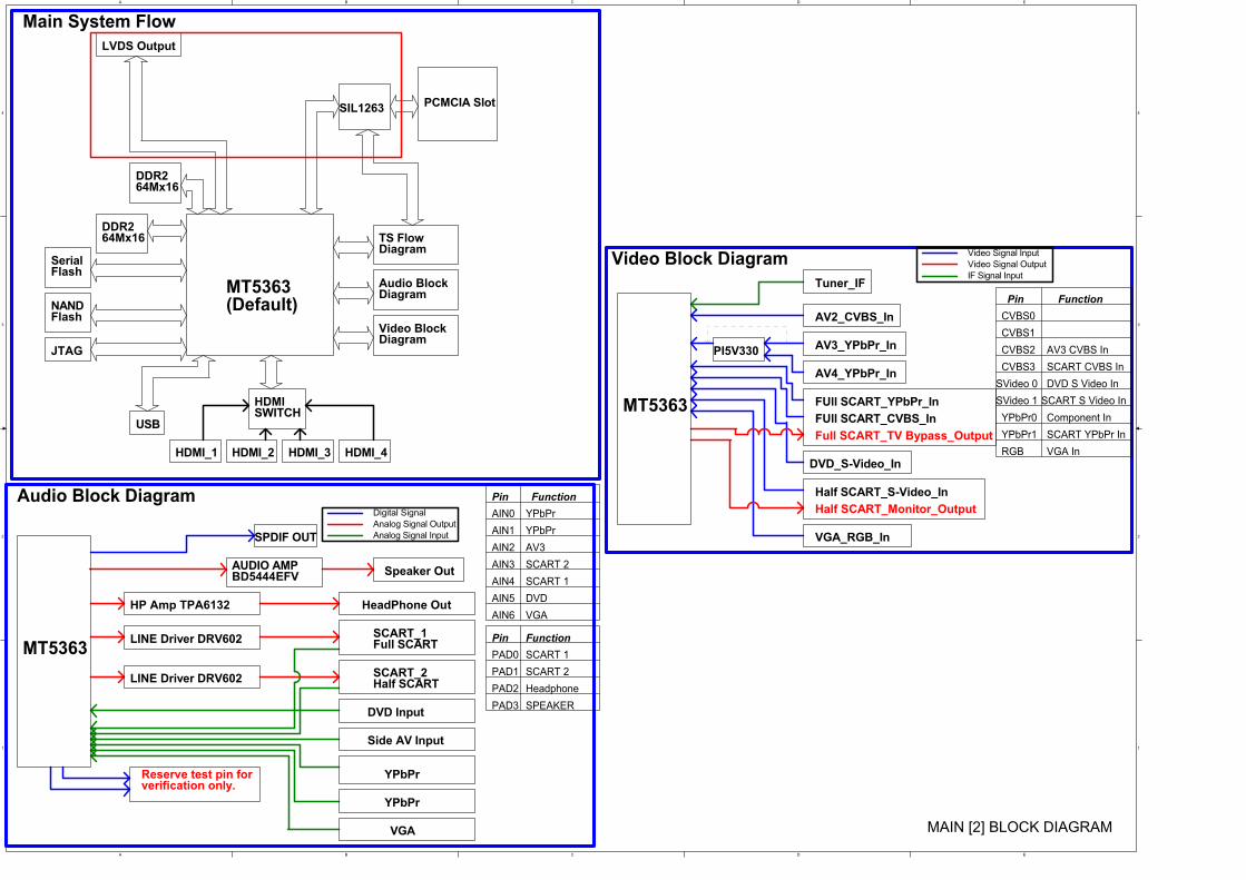
MT5363
Side AV Input
YPbPr
VGA
AUDIO AMPBD5444EFV
HP Amp TPA6132
Speaker Out
SPDIF OUT
HeadPhone Out
SCART_1Full SCART
SCART_2Half SCART
Reserve test pin forverification only.
Audio Block DiagramDigital Signal
Analog Signal Output
Analog Signal Input
AIN0
AIN1
AIN2
AIN3
AIN4
AIN5
AIN6
Pin
VGA
YPbPr
DVD
AV3
SCART 2
SCART 1
Function
FunctionPin
PAD0
PAD1
PAD2
SCART 1
Headphone
SCART 2
MT5363FUll SCART_CVBS_In
FUll SCART_YPbPr_In
AV2_CVBS_In
DVD_S-Video_In
Half SCART_Monitor_Output
Half SCART_S-Video_In
Full SCART_TV Bypass_Output
AV3_YPbPr_In
VGA_RGB_In
Tuner_IF
Video Block DiagramVideo Signal Input
Video Signal Output
IF Signal Input
CVBS0
Pin Function
CVBS1
CVBS2
CVBS3 SCART CVBS In
SVideo 0 DVD S Video In
SCART S Video InSVideo 1
YPbPr0 Component In
YPbPr1
VGA InRGB
SCART YPbPr In
MT5363(Default)
LVDS Output
DDR264Mx16
DDR264Mx16
SIL1263PCMCIA Slot
HDMI_1 HDMI_2
USB
SerialFlash
NANDFlash
JTAG
Audio Block Diagram
Video Block Diagram
Main System Flow
TS Flow Diagram
HDMISWITCH
HDMI_4HDMI_3
AV4_YPbPr_In
PI5V330
YPbPr
YPbPr
LINE Driver DRV602
LINE Driver DRV602
DVD InputPAD3 SPEAKER
AV3 CVBS In
MAIN [2] BLOCK DIAGRAM
A
A
B
B
C
C
D
D
E
E
4 4
3 3
2 2
1 1
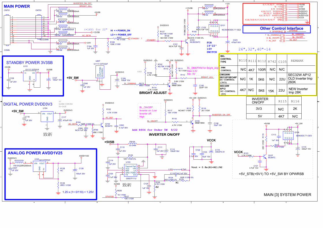
HI = > POWER_ON
LO = > POWER_OFF
MAIN POWER
STANDBY POWER 3V3SB
DIGITAL POWER DVDD3V3
Other Control Interface(+16V) for 22"
IC
G1084-33TU3Uf
TO-263T
1.25 x (1+ 0/110) = 1.25V
ANALOG POWER AVDD1V25
FOR
19"22"
16V
SWITCH
BL_ON/OFF
Inverter on: Low
Inverter off:
High
INVERTER ON/OFF
Add R904 for Under 5W 9/22
R1
Vout = 0.8x(R1+R2)/R2
R2
N/C 2K
4K7
INVERTERON/OFF
N/C5V
3V3
+5V_STB(+5V1) TO +5V_SW BY OPWRSB
R115 R116
BL_DIM(PWM for Bright_Adj):
Max:3.3V
Min: 0V0303
BRIGHT ADJUST
C105
5K6
R112
SEC32W
AP12
N/C100R
1K
R111
26",32",40"-14
BKL
CONTROL
TYPE
22U
4K7
CMO26W/
SEC32F/SEC40FDC-CONTROL
(3V3)
DC-CONTROL
(5V)
R110
N/CPWM
CONTROL
N/C
4K7
N/C
SEC32W AP12OLD Inverter lmp260K
N/C
22U5K6
R742
15K
N/C
REMARK
NEW Inverterlmp 28K
OPWRSB
AC_DET#
INVERTER_ON_OFF
BRIGHT_ADJ
AC_DET#
AC_DET
STANDBY
INVERTER_ON_OFF
BL_ON/OFF
OPWRSB
BL_DIMMING
BL_ON/OFF
AC_DET
BL_DIMMING
BRIGHT_ADJ
AVDD3V38,9,15,17
VCCK4GND4,5,6,7,8,9,10,11,12,13,14,15,16,17
+5VSB6,11,14,16,17
3V3SB6,16
OPWRSB6
STANDBY 7
AVDD1V254,5,7,8,15,17
DVDD3V34,5,6,7,9,17
+12V15
BL_DIMMING7
BL_ON/OFF8
AC_DET7
VCCK
+5VSB
3V3SB
AVDD3V3
+5VSB
3V3SB
+12VSB
+24V
+5VSB
DVDD3V3
AVDD1V25
DVDD3V3
+5V_SW
+12V
DVDD3V3
AVDD1V25
+12V
+12VSB
DVDD3V3+5V_SWDVDD3V3
+5VSB
3V3SB
VCCK
+5VSB
VCCK
+5V_SW
+5V_SW
AVDD3V3
DVDD3V3
DVDD3V3
DVDD3V3 +5V_SW DVDD3V3
R110
NC
/4K
7 1
/10W
C547
1uF 25V
Q101
NC/Si5403DC-T1-GE3
12345 6 7 8
DDDGS D D D
C552
0.1uF 50V
Q105MMBT3904
3
1
2
C125
1uF 16V
U607
G1117-33T43UF
123
AD
J(G
ND
)V
OU
T(T
AB
)V
IN
R104100R 1/10W 5%
R749
68K 1/10W
U103
G5627F11U
1234 5
6789
VCCREFGNDFB EN
PGNDLX
VINThermal Pad
+ C126
100uF 25V
C116
1uF 25V
C1214.7UF 10V
R108100K 1/10W
Q102BC847C
C122
0.1uF 50V
C1041uF 25V
Q104MMBT3904
3
1
2
C550NC/0.1uF 50V
FB109
33 OHMC111
1uF 25V
R112
5.6K 1/10W
C10810uF 10V
+ C115330uF 10V
C10522UF 10V
Q106
Si5403DC-T1-GE3
12345 6 7 8
DDDGS D D D
U104
3 2
1
VIN VOUT
GN
D
R120
10R 1/10W 5%
R103N
C/2
2K
1/1
0W
FB104
120R/6000mA1 2
R137NC/10K 1/10W
R102
4.7K 1/10W
+ C107100uF 10V
R1130R01 1/10W
R106NC/10K 1/10W
R1111K 1/10W
R12151K 1/10W
U105 G1117T63Uf
3
1
2
4
VIN
GN
D
VOUT
TH
R11710K 1/10W
L101 4.7uH
+C117
470uF/10V
C101NC/4.7UF 10V
FB103 120R/6000mA1 2
+ C323
470uF/16V
R1071K 1/10W
C546
1uF 25V
C102NC/4.7UF 10V
R118
4.7K 1/10W
Q107BC847C
R128NC
C114
1uF 25V
+ C109100uF 10V
FB105
120R/6000mA1 2
FB102 220R/2000mA1 2
C113
1uF 16V
R1290R01 1/10W
FB108 220R/2000mA1 2
R119
22K
1/1
0W
+ C112100uF/16V
U101
G1117-33T63Uf
3 2
1 4
VI VO
GN
D
4
CN703
NC/CONN
12345678910
R12710K 1/10W
Q103NC/BC847C
C120
0.1uF 50V
R1144.7K 1/10W
FB107 220R/2000mA1 2
R115NC/4K7 1/10W
C123
10uF 10V
C106
1uF 25V
FB135220R/2000mA
1 2
C110
1uF 25V
C118 NC/1nF 50V
R1264.7K 1/10W
FB139 120R/6000mA1 2
R105
NC/51K 1/10W 5%
R1094.7K 1/10W
FB101 220R/2000mA1 2
CN701
CONN
12345678910111213
R1241K8 1/10W 1%
R626
1K 1/10W
R1232.7K 1/10W
+ C119330UF6.3V
FB106 120R/6000mA1 2
R742NC/15K 1/10W
R125100R 1/10W 5%
R1162K 1/10W
MAIN [3] SYSTEM POWER
5
5
4
4
3
3
2
2
1
1
D D
C C
B B
A A
Bottom Side
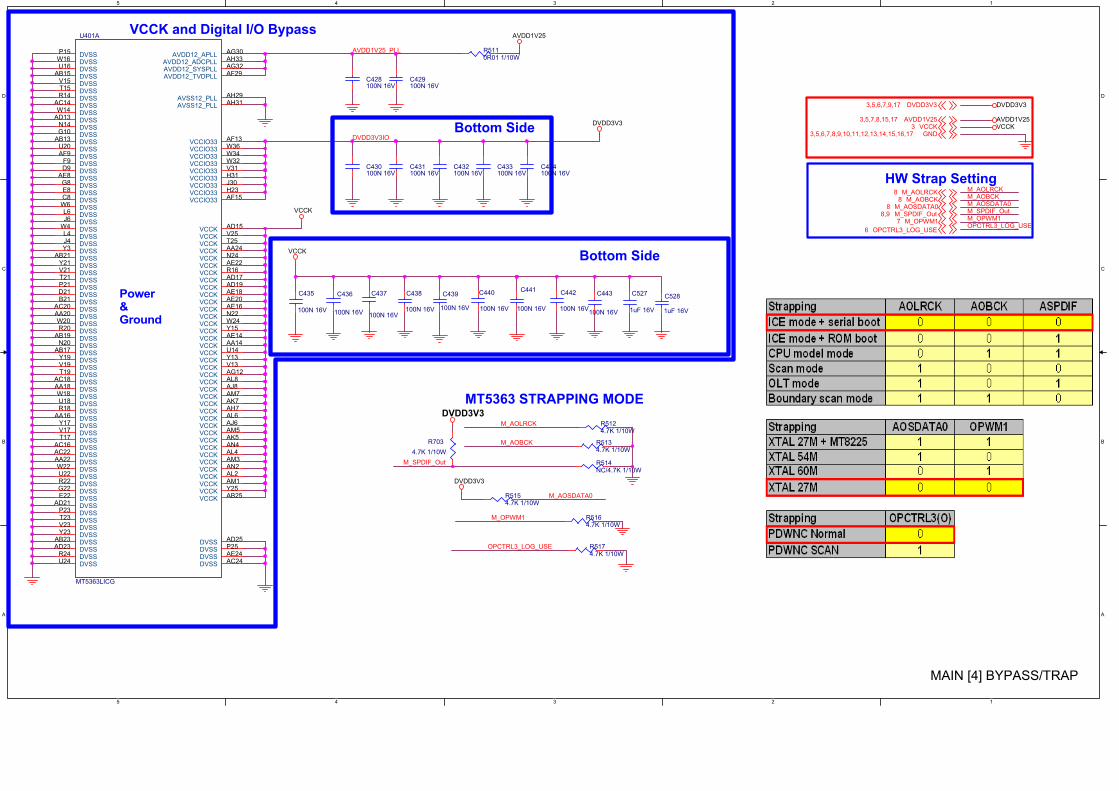
VCCK and Digital I/O Bypass
Bottom Side
HW Strap Setting
MT5363 STRAPPING MODE
AVDD1V25_PLL
M_SPDIF_OutM_OPWM1
M_AOLRCKM_AOBCKM_AOSDATA0
M_AOBCK
M_AOLRCK
M_OPWM1
M_AOSDATA0
OPCTRL3_LOG_USE
OPCTRL3_LOG_USE
M_SPDIF_Out
DVDD3V3IO
DVDD3V33,5,6,7,9,17
AVDD1V253,5,7,8,15,17
M_AOLRCK8
GND3,5,6,7,8,9,10,11,12,13,14,15,16,17VCCK3
M_AOSDATA08M_AOBCK8
M_OPWM17M_SPDIF_Out8,9
OPCTRL3_LOG_USE6
AVDD1V25
VCCK
DVDD3V3
VCCK
VCCK
DVDD3V3
AVDD1V25
DVDD3V3
DVDD3V3
R5134.7K 1/10W
C430100N 16V
C436
100N 16V
C442
100N 16V
C528
1uF 16V
Power&Ground
U401A
MT5363LICG
AF29AG32AH33AG30
Y3J4L4
W4J6L6
W6C8E8G8
AE8D9F9
AF9
G10AB13
AD13N14
R14
W14AC14
P15
T15V15
AB15U16W16
AA16
AC16T17V17Y17
AB17
R18U18W18
AA18AC18
T19V19Y19
AB19N20
R20
U20
W20AA20AC20
B21D21P21T21V21Y21
AB21
AD21E22G22R22U22W22
AA22AC22
AM1AL2AN2AM3AL4AN4AK5AM5AJ6AL6AH7AK7AM7AJ8AL8AG12V13Y13U14AA14AE14Y15
AD15
R16
AE16
AD17
AE18AD19
AE20
N22
AE22N24
W24
AA24T25V25
H23J30H31V31W32W34W36AF13
AH29AH31
P23T23V23Y23
AB23AD23
R24U24 AC24
AE24P25AD25
Y25AB25
AF15
AVDD12_TVDPLLAVDD12_SYSPLLAVDD12_ADCPLL
AVDD12_APLL
DVSSDVSSDVSSDVSSDVSSDVSSDVSSDVSSDVSSDVSSDVSSDVSSDVSSDVSS
DVSSDVSS
DVSSDVSS
DVSS
DVSSDVSS
DVSS
DVSSDVSSDVSSDVSSDVSS
DVSS
DVSSDVSSDVSSDVSS
DVSS
DVSSDVSSDVSSDVSSDVSSDVSSDVSSDVSS
DVSSDVSS
DVSS
DVSS
DVSSDVSSDVSSDVSSDVSSDVSSDVSSDVSSDVSSDVSS
DVSSDVSSDVSSDVSSDVSSDVSSDVSSDVSS
VCCKVCCKVCCKVCCKVCCKVCCKVCCKVCCKVCCKVCCKVCCKVCCKVCCKVCCKVCCKVCCKVCCKVCCKVCCKVCCKVCCKVCCK
VCCK
VCCK
VCCK
VCCK
VCCKVCCK
VCCK
VCCK
VCCKVCCK
VCCK
VCCKVCCKVCCK
VCCIO33VCCIO33VCCIO33VCCIO33VCCIO33VCCIO33VCCIO33VCCIO33
AVSS12_PLLAVSS12_PLL
DVSSDVSSDVSSDVSSDVSSDVSSDVSSDVSS DVSS
DVSSDVSSDVSS
VCCKVCCK
VCCIO33
C428100N 16V
C429100N 16V
C432100N 16V
C431100N 16V
R5174.7K 1/10W
R5164.7K 1/10W
C433100N 16V
R514NC/4.7K 1/10W
C439
100N 16V
C441
100N 16V
C443
100N 16V
R5110R01 1/10W
C438
100N 16V
C434100N 16V
R5124.7K 1/10W
R703
4.7K 1/10W
C440
100N 16V
C435
100N 16V
C437
100N 16V
C527
1uF 16V
R5154.7K 1/10W
MAIN [4] BYPASS/TRAP
5
5
4
4
3
3
2
2
1
1
D D
C C
B B
A A
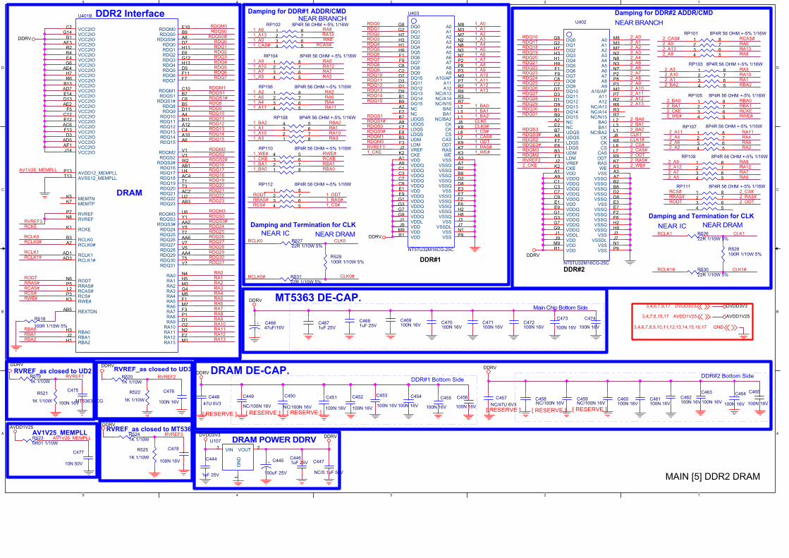
DDR#2 Bottom Side
[ RESERVE ]
DRAM DE-CAP.DDR#1 Bottom Side
[ RESERVE ] [ RESERVE ][ RESERVE ][ RESERVE ][ RESERVE ]
DDR2 InterfaceNEAR BRANCH
NEAR IC NEAR DRAM
Damping and Termination for CLK
Damping for DDR#1 ADDR/CMD
DDR#1
NEAR IC
DDR#2
Damping and Termination for CLK
NEAR DRAM
Damping for DDR#2 ADDR/CMD
NEAR BRANCH
RVREF_as closed to UD3
RVREF_as closed to MT5363AV1V25_MEMPLL
RVREF_as closed to UD2
MT5363 DE-CAP.Main Chip Bottom Side
DRAM POWER DDRV
RDQ27
RODT
RCAS#
RCLK1#
RRAS#
RDQS2#
RDQ18
RA8
RDQ10
RA2
RDQ0
RCLK1
RDQ16
RA6
RDQ3
RA13
RDQM2
RDQS3#
RDQ19
RA12
RA3
RDQ8
RDQ24
RDQS1#
RA5
RDQ9
RDQS0#
RDQ2
AV1V25_MEMPLL
RDQ20
RDQ25
RA9
RWE#
RDQ17
RA1
RDQ22
RBA0
RA7
RDQ1
RDQ12
RA10
RCKE
RDQ6
RDQM0
RVREF3
RBA1
RDQ29
RDQ14
RCS#
RDQS2
RDQM3
RDQ5
RDQM1
RDQ7
RDQ30
RDQS0
RCLK0
RA11
RDQ31
RDQ26
RDQ11
RDQS1
RDQ15
RDQ21
RDQ13
RDQS3
RA0
RDQ23
RDQ28
RDQ4
RA4
RBA2
RCLK0#
1_A5
1_CKE
CLK0
RDQ11
RBA0
1_WE#
RCAS#
1_A4
1_A2
1_CAS#
RDQ15
1_CS#
1_A12
RDQ6
CLK0#RDQS0#
RDQ10
1_CKE
RCLK0#
1_A7
RCLK0
1_RAS#
1_A11
1_A6
1_A6
1_CS#
RDQ3
RDQS1
RA8
1_CAS#
1_ODT
RDQ2
RDQ14
1_BA0
RA5
RA12
1_BA11_BA0
RDQ5
1_A9 1_A7
1_WE#
RDQ4
RDQ1
RDQM1
RWE#
RA9
RDQ91_A12
1_A1RDQ0
RDQS0
1_BA1
1_A31_A2
1_RAS#RDQM0
RCKE
RA13
RRAS#
1_A13
1_A8
1_A0
RDQ7
1_A10
RDQ13
RDQS1#
1_A5
1_A13
RCS#
RODT
RDQ12
1_A9
1_A4
1_BA2
RVREF1
RA0
1_ODT
RDQ8
RBA1
RA7
1_A0
1_A8
1_A11
1_BA2RA1
1_A3
RBA2
RA31_A101_A1
RA10
RA2
RA4RA11
RA6
CLK0
CLK0#
2_A8
2_A11
2_A6
RA0
RCLK1
RDQ22
RBA0
2_CKE
2_A1
2_BA2
CLK1#
RBA1
RDQ27
CLK1#2_CS#
2_A13
2_RAS#
RA11
2_ODT
RDQS2#
2_A0
2_A5
RBA2
2_A3
RA12
RVREF2
2_CKE
RDQM3
RCLK1#
RDQS2
RA8
2_A4
2_BA0
RA2RA6
RDQ20
2_WE#
RA10
2_A0
2_A9RDQ25
2_A7
RDQ21
RA4
RA3
2_A7
RWE#
RA13
2_BA0
2_A11
RDQ23
RDQ16
RDQ28
RRAS#
2_A12
RDQ17
2_A2
RDQM2
RDQ18
RCKE
2_A10
2_ODTRODT
RCAS#
RA7
RDQS3
CLK1
RDQ31
RDQ29
2_A5
2_A12
2_A4
2_A13
2_A1
2_BA1
RA9
2_A10
2_A2
2_CAS#
2_A3
RDQ30
2_A9
RCS#
CLK1
2_CS#
RDQ24
2_BA1
RA1
2_A8
RDQS3#
RDQ26
2_CAS#
2_A6
RDQ19
2_RAS#
2_BA2
2_WE#
RA5
RVREF3AV1V25_MEMPLL
RVREF1 RVREF2
AVDD1V253,4,7,8,15,17
GND3,4,6,7,8,9,10,11,12,13,14,15,16,17
DVDD3V33,4,6,7,9,17
DDRV
DDRV
DDRV
DDRV DDRV
DDRVAVDD1V25
DDRV
DVDD3V3
AVDD1V25
DDRVDDRV
DDRVDVDD3V3
C454
100N 16V
C462100N 16V
C453
100N 16V
C463
100N 16V
U107
3 2
1
VIN VOUT
GN
D
R522
1K 1/10WC451
100N 16V
U402
NT5TU32M16CG-25C
A1
A2
A3A7
A8
A9
B1
B2
B3
B7
B8
B9
C1
C2
C3C7
C8
C9
D1
D2
D3D7
D8
D9
E1
E2
E3E7
E8
E9
F1
F2
F3
F7
F8
F9
G1
G2
G7
G8
G9
H1
H2
H3H7
H8
H9
J1
J2
J3J7
J8
J9
K2 K3K7
K8
K9
L1
L2L3
L7L8
M2
M3M7
M8
M9 N1
N2
N3N7
N8
P2
P3
P7
P8
P9R1
R2
R3R7
R8
G3
VDD
NC
VSSVSSQ
UDQS
VDDQ
DQ14
VSSQ
UDM
UDQS
VSSQ
DQ15
VDDQ
DQ9
VDDQVDDQ
DQ8
VDDQ
DQ12
VSSQ
DQ11DQ10
VSSQ
DQ13
VDD
NC
VSSVSSQ
LDQS
VDDQ
DQ6
VSSQ
LDM
LDQS
VSSQ
DQ7
VDDQ
DQ1
VDDQ
DQ0
VDDQ
DQ4
VSSQ
DQ3DQ2
VSSQ
DQ5
VDDL
VREF
VSSVSSDL
CK
VDD
CKE WERAS
CK
ODT
NC/BA2
BA0BA1
CASCS
A10/AP
A1A2
A0
VDD VSS
A3
A5A6
A4
A7
A9
A11
A8
VSSVDD
A12
NC/A14NC/N15
NC/A13
VDDQ
R525
1K 1/10W
C461100N 16V
RP110 8P4R 56 OHM +-5% 1/16W
1234
8765
RP103 8P4R 56 OHM +-5% 1/16W
1234
8765
C465
100N 16V
RP109 8P4R 56 OHM +-5% 1/16W
1234
8765
C474
100N 16V
R53122R 1/10W 5%
C4681uF 25V
C471100N 16V
R521
1K 1/10W
RP104 8P4R 56 OHM +-5% 1/16W
1234
8765
C478
100N 16V
C470100N 16V
C472100N 16V
C4671uF 25V
RP111 8P4R 56 OHM +-5% 1/16W
1234
8765
DRAM
U401B
MT5363LICG
N6
L2
N2
D1
K3
T3
V1
Y1
U4
AD3
P5
M5
H5
G2
U2
W2
AA2
AC4
P3
P1
K1
H1
AC2
V3
T1
AD1
A2
N4
J2
F1
AB3
T7
AB1
B3
M7
E2
G4
V5
U6
V7
AB5
B5
A4
M3
H3
AA4
Y5
D11
D7
F3
T5Y7
AA6
C6
B11
D5
B7
F11
G12
A8B9E10
E6
A6
C10
H13
F7
C4A10
H11
A12
B1
AF1
C2
R2
AE2
D3
AF3
E4R4
AE4
F5
AD5
G6
R6
AC6
H7
AD7
C12E12
B13
D13
F13
E14
G14
M1
P7N8
P13T13
K7K5
J14
RODT
RCAS#
RA11
RA9
RWE#
RDQ20
RDQM2
RDQS3
RDQ17
RCLK1#
RRAS#
RA4
RA1
RA10
RDQ22
RDQS2#
RDQS3#
RDQ18
RCS#
RA8
RCKE
RBA2
RDQ21
RDQS2
RDQ19
RCLK1
RCLK0#
RA0
RBA1
RA5
RDQ23
RDQ25
RDQ16
RCLK0
RA6
RA12
RA3
RDQ28
RDQM3
RDQ27
REXTDN
RDQ8
RDQ10
RA2
RBA0
RDQ29
RDQ24
RDQ9
RDQ0
RA7
RDQ30RDQ31
RDQ26
RDQS1#
RDQ11
RDQ5
RDQS1
RDQ6
RDQ3
RDQS0#RDQS0RDQM0
RDQ2
RDQ15
RDQM1
RDQ4
RDQ7
RDQ13RDQ14
RDQ1
RDQ12
VCC2IO
VCC2IO
VCC2IO
VCC2IO
VCC2IO
VCC2IO
VCC2IO
VCC2IOVCC2IO
VCC2IO
VCC2IO
VCC2IO
VCC2IO
VCC2IO
VCC2IO
VCC2IO
VCC2IO
VCC2IOVCC2IO
VCC2IO
VCC2IO
VCC2IO
VCC2IO
VCC2IO
RA13
RVREFRVREF
AVDD12_MEMPLLAVSS12_MEMPLL
MEMTPMEMTN
VCC2IO
C448
47U 6V3
C444
1uF 25V
C476
100N 16VC452
100N 16V
R52622R 1/10W 5%
C4461uF 25V
RP101 8P4R 56 OHM +-5% 1/16W
1234
8765
C450
NC/100N 16V
+ C46647uF/16V
C458NC/100N 16V
C475
100N 16VC459NC/100N 16V
R5241K 1/10W
R52722R 1/10W 5%
RP102 8P4R 56 OHM +-5% 1/16W
1234
8765
+C445
100uF 25V
C460100N 16V
C477
10N 50V
C473
100N 16V
C464
100N 16V
RP112 8P4R 56 OHM +-5% 1/16W
1234
8765
R518
100R 1/10W 5%
C449
NC/100N 16V
R528100R 1/10W 5%
RP106 8P4R 56 OHM +-5% 1/16W
1234
8765
U403
NT5TU32M16CG-25C
A1
A2
A3A7
A8
A9
B1
B2
B3
B7
B8
B9
C1
C2
C3C7
C8
C9
D1
D2
D3D7
D8
D9
E1
E2
E3E7
E8
E9
F1
F2
F3
F7
F8
F9
G1
G2
G7
G8
G9
H1
H2
H3H7
H8
H9
J1
J2
J3J7
J8
J9
K2 K3K7
K8
K9
L1
L2L3
L7L8
M2
M3M7
M8
M9 N1
N2
N3N7
N8
P2
P3
P7
P8
P9R1
R2
R3R7
R8
G3
VDD
NC
VSSVSSQ
UDQS
VDDQ
DQ14
VSSQ
UDM
UDQS
VSSQ
DQ15
VDDQ
DQ9
VDDQVDDQ
DQ8
VDDQ
DQ12
VSSQ
DQ11DQ10
VSSQ
DQ13
VDD
NC
VSSVSSQ
LDQS
VDDQ
DQ6
VSSQ
LDM
LDQS
VSSQ
DQ7
VDDQ
DQ1
VDDQ
DQ0
VDDQ
DQ4
VSSQ
DQ3DQ2
VSSQ
DQ5
VDDL
VREF
VSSVSSDL
CK
VDD
CKE WERAS
CK
ODT
NC/BA2
BA0BA1
CASCS
A10/AP
A1A2
A0
VDD VSS
A3
A5A6
A4
A7
A9
A11
A8
VSSVDD
A12
NC/A14NC/N15
NC/A13
VDDQ
C456
100N 16V
R5201K 1/10W
R5191K 1/10W
R53022R 1/10W 5%
R529100R 1/10W 5%
RP108 8P4R 56 OHM +-5% 1/16W
1234
8765
RP107 8P4R 56 OHM +-5% 1/16W
1234
8765
C455
100N 16V
R5230R01 1/10W
C457
NC/47U 6V3
RP105 8P4R 56 OHM +-5% 1/16W
1234
8765
C447
NC/0.1uF 50V
C469100N 16V
MAIN [5] DDR2 DRAM
5
5
4
4
3
3
2
2
1
1
D D
C C
B B
A A
Audio Mute/Digital Amp Control
Other Control Interface
HW Strap Pins
SCART Interface
NEAR IC
NEAR IC
256K
54MHz CRYSTAL
RESET Circuit
SYSTEM EEPROM
I2C ADDRESS "A0"
HI = > WRITELO = > WP
FOR CODE DOWNLOAD AND DEBUGGING
UART Port 0
NAND FLASH
NAND Flash
JTAG
16M
JTAG Port
colby 0624
TO IR/KEY BOARD
Toshiba Log Use
33G3802 3B FP
SCART_FS1SCART_FS0
OPWRSB
OXTALI
OSDA0OSCL0 U0RX
U0TX
POCE0#
JTRST#
PAALE
AVDD3V3_XTAL
LED_EPG_GREEN
PDD6
PDD3
POWE#
SCART_FS1
VCXO
PDD5
OXTALO
PDD2
Light_Sensor
OIRI
JTDI
PARB#
PDD7
AVDD3V3_XTAL
U1TX
KEY_UP_DN_DCSW
OXTALO
OSCL0
AVDD3V3_REG
U0TX
LED_POWER_RED
JTCK
PDD4
PDD0
KEY_MENU_L_R_SOURCE
AVDD3V3_REG
U1RX
JTDOJTMS
POOE#
POCE0#
OPWRSB
LED_EPG_RED
PDD1
SCART_FS0
U0RX
OSDA0
PACLE
1V0SB
1V0SBPOCE1#
OXTALI
E_FUSE
LED_POWER_GREEN
PDD5
PACLE
POCE1#
PDD3POWE#
PDD0
PDD2PAALE
PDD4PARB#
PDD7
PDD1
PDD6
POOE#
JTRST#
POCE0#PDD0
Flash_WP#
Flash_WP#
SP_AMP_MUTE
JTDO
POOE#PDD1 SYS_EEPROM_WP
JTAG_DBGRQ
TVTREF#1
JTCK
JTDIJTMS
JTAG_DBGACK
SP_AMP_MUTE
KEY_UP_DN_DCSW
Light_SensorOIRI
KEY_MENU_L_R_SOURCE
SYS_EEPROM_WPHD_SW
LED_EPG_GREENLED_POWER_RED
LED_EPG_RED
LED_POWER_GREEN
ORESET#
ORESET#
OPCTRL3_LOG_USE
OPCTRL3_LOG_USE
OPCTRL3_LOG_USE
DVDD3V33,4,5,7,9,17
+5VSB3,11,14,16,173V3SB3,16
SCART_FS112SCART_FS012
OPWRSB3
DVD_RX 8DVD_TX 8
U0RX 14U0TX 14
GND3,4,5,7,8,9,10,11,12,13,14,15,16,17
SP_AMP_MUTE11
HD_SW 10
HDMI_SW_SDA 8,17HDMI_SW_SCL 8,17
OPCTRL3_LOG_USE4
+5VSB3V3SB
DVDD3V3
1V0SB
DVDD3V3
DVDD3V3DVDD3V3DVDD3V3DVDD3V3
+5VSB
DVDD3V3DVDD3V3
3V3SB
3V3SB
3V3SB
DVDD3V3
DVDD3V3 DVDD3V3
DVDD3V3
DVDD3V3
3V3SB 3V3SB
+5VSB
+5VSB
3V3SB
FB110
600R/200mA
12
R557 100R 1/10W 5%
L116
NC/0.82UH
R549
4.7
K 1
/10W
U410MAX809STRG
1
2
3 GND
RE
SE
T
VCC
U608
NC/MX25L4005AMI-12G
1234 5
678CS
SOWPGND SI
SCKHOLD
VCC
CN702
NC/CONN
123
C482
NC/1nF 50V
C483100N 16V
R53610K 1/10W
R5624.7K 1/10W
R57210K 1/16W
+
C127
100uF 4V
C489
0.1
uF
50V
C559
10uF 10V
C492
0.1
uF
50V
R565 100R 1/10W 5%
R545 4.7K 1/10W
R5513.9K 1/10W
C490
NC
/0.1
uF
50V
C694
0.1
uF
50V
R569
1K 1/10W
R553 100R 1/10W 5%
R5630R01 1/10W
R570
27K 1/10W
R534
0R01 1/10W
R567 10K 1/16W
C486
33PF 50V
R556 100R 1/10W 5%
R57110K 1/10W
R558 100 OHM 1% 1/10W
Q126
MMBT3906 PNP
R5661K 1/10W
C479
100N 16V
C4950.1uF 50V
R550
3.9K 1/10W
R554 100R 1/10W 5%
R535
1R 1/10W 5%
R568
10K 1/16W
R541
1K8 1/10W 1%
TP403
TP401
R5474.7K 1/10W
C4844U7 10V
R706 100R 1/10W 5%R555 100R 1/10W 5%
R573
33R 1/10W 5%
R5614.7K 1/10W
RP113
10KOHM +-5% 1/16W
1234
8765
C487
1uF
25V
CN119
NC/60693 3P 2.0mm
123
R5334.7K 1/10W
R559 100 OHM 1% 1/10W
R542
100K 1/10W
Q127MMBT3904
3
1
2
R56468K 1/10W
R5320R01 1/10W
U405
HY27US08281A-TPCB
123456789
101112131415161718192021222324 25
2627282930313233343536373839404142434445464748NC
NCNCNCNCNCR/BRECENCNCVCCVSSNCNCCLEALEWEWPNCNCNCNCNC NC
NCNCNC
I/O0I/O1I/O2I/O3NCNCNC
VSSVCCPRE
NCNC
I/O4I/O5I/O6I/O7NCNCNCNC
R5524.7K 1/10W
C491
0.1
uF
50V
C494
0.1
uF
50V
CN406
NC/60947 20P 1.25MM
13579
1113151719
2468101214161820
21
22
R5604.7K 1/10W
C493
0.1
uF
50V
R537
820R
1/1
0W
1%
R544 330 OHM 1/10W
C481
1PF50V
R546 4.7K 1/10W
C488
1uF
25V
STB I/F &Peripheral
U401C
MT5363LICG
AM23
AN24AL24
AK37AK35
AJ34
AM35
AM37
AL32
AJ36
AL34
AL36
AK33
AT1
AR2AU2
AP5
AN6
L30
AT3AT5AU4AR4
AU6AR6
AT7AP7
AU8AR8
AP1AP3
P33P31
R32R34
AK1AJ2AK3AJ4AH5
T35R36
T37
AM19AN20
AM21
AR20AU20
AN22
AL20AL22
AP21AT21
AVDD10_LDO
AVDD33_VGA_STBAVSS33_VGA_STB
AVSS33_XTALAVDD33_XTAL_STB
XTALO
ADIN2_SRV
ADIN4_SRV
ADIN0_SRV
XTALI
ADIN3_SRV
ADIN5_SRV
ADIN1_SRV
POCE0#
PDD0POOE#
PDD1
POCE1#
FSRC_WR
POWE#PARB#PACLEPAALE
PDD3PDD2
PDD5PDD4
PDD7PDD6
OSDA0OSCL0
OSDA2OSCL2
OSDA1OSCL1
JTRST#JTDI
JTCKJTMSJTDO
U1TXU1RX
VCXO
OPCTRL1OPCTRL2
OPCTRL0
OPCTRL3OPCTRL4
OIRI
OPWRSBORESET#
U0TXU0RX
U609
M24C32-WMN6TP
4
8
56
123
7
VSS
VCC
SDASCL
E0E1E2
WC
C480
1PF50V
R548
4.7
K 1
/10W
X401
54.000MHz
12
CN401
CONN
123456789
1011121314
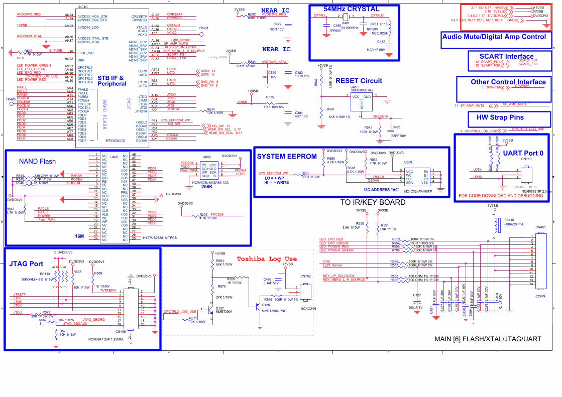
MAIN [6] FLASH/XTAL/JTAG/UART
5
5
4
4
3
3
2
2
1
1
D D
C C
B B
A A
Function 1 (Internal CI) CI Interface
LVDS Control Interface
For CID Test Only
Closed to Main Chip
Closed to PCMCIA
HW Strapping
PCMCIA 5V Slot
4M,16M,20M,24M,27MHz
TDA10024
CLOSE TO CI CONNECTOR
Near Connector
LO=> OCHI = > NORMAL
M_CI_OUTDATA2
M_CI_INDATA2M_CI_INDATA1
M_CI_INDATA3M_CI_INDATA4M_CI_INDATA5
M_CI_INVALID
M_CI_INDATA6M_CI_INDATA7
M_CI_OUTVALID
M_CI_OUTDATA0M_CI_OUTSYNC
M_CI_OUTDATA1
CI_OUTSYNC
CI_OUTDATA2
CI_OUTDATA0CI_OUTDATA1
CI_OUTVALID
CI_INDATA1CI_INDATA2
CI_INDATA5
CI_INVALID
CI_INDATA4CI_INDATA3
CI_INDATA7CI_INDATA6
M_CI_INSYNC
CI_OUTDATA3M_CI_OUTDATA3
M_CI_OUTDATA6
CI_OUTDATA4
M_CI_INDATA0
CI_OUTDATA6CI_OUTDATA7
CI_OUTDATA5M_CI_OUTDATA4
CI_INDATA0CI_INSYNC
M_CI_OUTDATA7
M_CI_OUTDATA5
CI_WAIT#CI_OUTCLK
BL_DIMMING
M_OPWM1
CI_OUTCLKM_CI_OUTCLK
CI_IREQ#
M_CI_INCLK
USB_PWR_EN
USB_PWR_OCP
AUDIO_MUTE
AC_DET
M_GPIO2
M_CI_OUTDATA1
M_CI_INDATA6
CI_D6
M_GPIO2
CI_A10
USB_PWR_EN
BL_DIMMING
M_CI_INSYNC
M_CI_OUTDATA2
UART_SW
CI_A14
CI_A7
M_CI_INVALID
M_CI_INCLK
CI_A13
M_CI_INDATA7
CI_CD2#
M_OPWM1
CI_D7
M_CI_OUTDATA5
CI_A1
CI_VS1#CI_A3
CI_A12
M_CI_INDATA5
AC_DET
CI_D5
CI_D2
CI_A2
CI_WE#
M_CI_OUTDATA0
CI_CE1#
M_CI_OUTVALID
M_CI_OUTDATA3
M_CI_OUTSYNC
SYS_RESET
STANDBY
CI_CD1#
M_CI_INDATA1
CI_REG#
CI_A0
USB_PWR_OCP
CI_D4
M_CI_INDATA2
CI_IORD#CI_A6
CI_D3
TD0
M_CI_INDATA0
M_OPWM0
CI_A4
M_CI_INDATA3
CI_A9
TVALID
CI_IREQ#
TSYNC
CI_PWR_OC
M_CI_OUTCLK
CI_OE#
CI_WAIT#
TCK
CI_D0
M_CI_INDATA4
M_CI_OUTDATA4
M_CI_OUTDATA6
CI_A5CI_RESET
CI_A11
CI_PWR_EN
AUDIO_MUTE
CI_IOWR#
M_CI_OUTDATA7
CI_D1
CI_A8
HP_DET#
Si2163_TS_CLK
Si2163_ADDR
SDA_TUSCL_TU
AV12_A
TUNER_CLK
Si2163_D7
TUNER_DATA
IF_AGC
Si2163_ADDR
Si2163_D1CI_INDATA2
Si2163_D0
CI_INDATA3
CI_INDATA1Si2163_D2Si2163_D3
Si2163_TS_CLK
Si2163_D6
TSYNC
Si2163_TS_VALCI_INCLK
CI_INSYNC
TVALID CI_INVALIDCI_INDATA7
Si2163_D5CI_INDATA6
Si2163_TS_SYNC
CI_INDATA5
TCK
Si2163_D7
SCL_TUTUNER_DATA
TUNER_CLK
SDA_TU
CI_A5
CI_INVALID
CI_INDATA6
CI_CE2#CI_OUTDATA7
CI_VS1#
CI_OUTDATA3
CI_OUTVALID
CI_D1
CI_INDATA3
CI_OUTDATA4
CI_CD2#
CI_A0
CI_REG#
CI_RESET
CI_CD1#
CI_OUTDATA0
CI_CE1#
CI_WAIT#
CI_A9
CI_OE#
CI_OUTDATA2
CI_A14
CI_A11
CI_INDATA7
CI_INDATA5
CI_OUTDATA6CI_OUTDATA5
CI_A6
CI_OUTDATA1
CI_INSYNC
CI_A7
CI_A3
CI_A1
CI_D5
CI_IORD#
CI_A13
CI_A4
CI_OUTCLK
CI_IOWR#
CI_INCLK
CI_INDATA1
CI_A12
CI_A10
CI_A8
CI_IREQ#
CI_INDATA0
CI_A2
CI_D0
CI_CD1#
CI_D4
CI_D2
CI_WE#
CI_CD2#
CI_INDATA2
CI_OUTSYNC
CI_D7CI_D6
CI_INDATA4
CI_D3
CI_INDATA4Si2163_D4
TD0 CI_INDATA0
Si2163_D1
Si2163_D5
CI_CE2#
SYS_RESET
Si2163_D0
Si2163_TS_VAL
Si2163_D4
Si2163_TS_SYNC
Si2163_D6
Si2163_D2Si2163_D3
CI_VS1#
HP_DET#
CI_PWR_OCCI_PWR_EN
M_OPWM0
M_AOLRCK
CI_INCLK
CI_INCLK
Si2163_TS_CLK
M_AOLRCK
DVDD3V33,4,5,6,9,17
BL_DIMMING3
M_OPWM14
USB_PWR_EN17
USB_PWR_OCP17
AUDIO_MUTE11
AC_DET3
M_GPIO213
STANDBY 3
UART_SW 14
IF_AGC13
TUNER_DATA8TUNER_CLK8
SDA_TU13SCL_TU13
VIP13
VIM13
AVDD1V253,4,5,8,15,17
IF_AGC13
GND3,4,5,6,8,9,10,11,12,13,14,15,16,17
HP_DET# 9
M_OPWM013
M_AOLRCK8
DVDD3V3
CI2_VCC
CI2_VCCCI2_VCC
DVDD3V3DVDD3V3
DVDD3V3AVDD_1V25
AV
DD
_1V
25
AVDD_1V25 Si2163_VDDH_ANA
AVDD_1V25AVDD1V25
AVDD1V25AVDD_1V25
CI2_VCCCI2_VCC
Si2163_VDDH_ANA
DVDD3V3
DVDD3V3
DVDD3V3
DVDD3V3
DVDD3V3
DVDD3V3
+5V_SWCI2_VCC
DVDD3V3
R704
NC/0R01 1/10W
TP405
FB134 80 OHM
1 2
R614 10K 1/10W
U610
Si21631 2 3 4 5 6 7 8 9 10
293031
3332
343536
28
27
26
25
24
23
22
21
20
19
111213
151617
14
18
37G
ND
AG
C_IF
AG
C_R
FS
CL_H
OS
TS
DA
_H
OS
TV
DD
_C
OR
ET
S_V
AL
TS
_S
YN
CT
S_C
LK
GN
D
ADC_IPADC_INADC_CP
SDA_MASTADC_CN
SCL_MASTRESSI_ADCGPIO_0
VD
D_V
AD
CV
DD
H_A
NA
AD
DR
XT
AL_I
XT
AL_O
VD
D_V
CO
RE
RE
SE
TB
TS
_E
RR
/GP
IO_2
TS
_D
AT
A7
GN
D
TS_DATA0TS_DATA1TS_DATA2
VDD_HVIOTS_DATA4TS_DATA5
TS_DATA3
TS_DATA6
GND
FB136
80 OHM
1 2
R620 10K 1/10W
R136 0R01 1/10W
C568
10N
50V
C700
100N 16V
R57510K 1/10W
C50610pF 50V
X402
16MHZ 20P
12
R581 22R 1/10W 5%
R587 22R 1/10W 5%
R134 0R01 1/10W
TP404
R61210K 1/10W
GPIO/Int. CI/ MII
U401H
MT5363LICG
F23D23A22C22
E24J24B23
B25D25C24G24
C26J26F25H25
D27G26E26A26
G28H27F27B27
D29C28E28J28
E30H29F29B29
A30C30G30
F31
B31D31
G32
A32C32E32
B33
D33
F33
H33
A34C34
E34
G34
B35
D35
G36
H35
A36
C36
E36
H37
B37
D37
F37
F35
AH1
AG2AF5
AH3
AG4
AE6
AG6
AF7
J32
K35K37
J34
T33J36
GPIO33GPIO34GPIO35GPIO36
GPIO30GPIO31GPIO32
GPIO26GPIO27GPIO28GPIO29
GPIO22GPIO23GPIO24GPIO25
GPIO18GPIO19GPIO20GPIO21
GPIO14GPIO15GPIO16GPIO17
GPIO10GPIO11GPIO12GPIO13
GPIO6GPIO7GPIO8GPIO9
GPIO3GPIO4GPIO5
ETPHYCLK
ETTXD3ETTXEN
ETCOL
ETTXD0ETTXD1ETTXD2
ETRXCLK
ETTXCLK
CI_MCLKO
CI_MISTRT
ETRXD2ETRXD3
ETTXER
CI_MIVAL
ETRXD1
ETRXER
CI_MOVAL
CI_MDI0
ETRXD0
ETCRS
ETMDC
CI_MDO0
ETRXDV
ETMDIO
CI_MOSTRT
CI_MCLKI
GPIO44
GPIO38GPIO37
GPIO43
GPIO41
GPIO39
GPIO42
GPIO40
GPIO2
GPIO0GPIO1
OPWM0
OPWM2OPWM1
R604 0R01 1/10W
R627 0R01 1/10W
R603 0R01 1/10W
R577 22R 1/10W 5%
R617 10K 1/10W
R684 100R 1/10W 5%
R583 22R 1/10W 5%
C510
0.1
uF
50VR578 22R 1/10W 5%
R579 22R 1/10W 5%
R601 0R01 1/10W
R712 4.7K 1/10W
R624 NC/0R01 1/10W
C511
0.1
uF
50V
R576 22R 1/10W 5%
R589 22R 1/10W 5%
C593
27PF 50V
U130TS5A3157DCKR
123 4
56NO
GNDNC COM
V+IN
TP407
C5140.1uF 50V
R615 10K 1/10W
C562
0.1uF 50V
C5130.1uF 50V
C508
0.1
uF
50V
C594
27PF 50V
R610 0R01 1/10W
R713 4.7K 1/10W
R585 22R 1/10W 5%
R625 NC/0R01 1/10W
R591 22R 1/10W 5%
R595 22R 1/10W 5%
+ C566100uF 16V
R59847 OHM 1/10W
C509
0.1
uF
50V
R584 22R 1/10W 5%
R606 0R01 1/10W
R135 NC/0R01 1/10W
C69910uF 10V
R592 22R 1/10W 5%
R580 22R 1/10W 5%
FB111
220R/2000mA1 2
C497
10pF 50V
R611 0R01 1/10W
FB133220R/2000mA
1 2
R596 22R 1/10W 5%
C567
100N 16V
C59110uF 10V
R618 10K 1/10W
+ C496100UF16V
R683 100R 1/10W 5%
R582 22R 1/10W 5%
R694
0R01 1/10W
R672
100R 1/10W 5%
R609 0R01 1/10W
R60510K 1/10W
R600 0R01 1/10W
U114
G5250H1T1U
1
2
3
4 5
OUT GN
D
IN
EN(EN) OC
R197
4.7K 1/10W
C592
0.1uF 50V
R680
1K
1/1
0W
R602 0R01 1/10W
R590 22R 1/10W 5%
C598
0.1
uF
50V
R61310K 1/10W
R58647 OHM 1/10W
R588 22R 1/10W 5%
R705
0R01 1/10W
PCMCIA
CN159
JACK
2019
7
9
1516
1
34
303132
23456
2928272625242322
1211
8
10
21
1314
33
1817
68676665646362
353637383940414243444546474849505152535455565758596061
69
70
71
72
A15A16
CE1#
OE#
WE#RDY/BSY
GND
GND
D0D1D2
D3D4D5D6D7
A0A1A2A3A4A5A6A7
A8A9
A10
A11
A12
A13A14
WP
VPP1VCC
GNDCD2#
D10D9D8
BVD1BVD2
GNDCD1#
D11D12D13D14D15
CE2#RFSH
RFURFUA17A18A19A20A21
VCCVPP2
A22A23A24A25RFU
RESETWAIT#
RFUREG#
69
70
71
72
R597 0R01 1/10W
R671 100R 1/10W 5%
R593 22R 1/10W 5%R594 22R 1/10W 5%
R607 0R01 1/10W
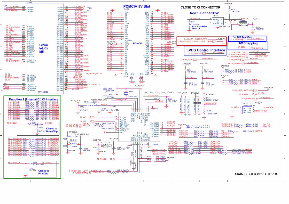
MAIN [7] GPIO/DVBT/DVBC
5
5
4
4
3
3
2
2
1
1
D D
C C
B B
A A
Audio Input
Audio Output
Video Input Video Output
Tuner I/O Interface
LVDS Control InterfaceSPDIF
NEAR IC
HW Strap Setting
For POP Nouse
Near IC
AV3(CVBS)_Audio R/L
AV3_AUDIO(Side) DVD_AUDIO
FOR MEMC UART AND I2C
SCART2_Out_RSCART2_Out_L
HP_Out_LHP_Out_R
SCART1_Out_R
SCART1_Out_L
VGA_L_InVGA_R_In
SCART1_L_InSCART1_R_In
SCART2_L_InSCART2_R_In
COM1
COM0
GP
PR1P
COM
SOY1
SOY0
VSYNC
RP
Y0P
Y1P
HSYNC
PB0P
SOG
PB1P
Moniter_OutTuner_ByPass_Out
FAT_IN-FAT_IN+
IF_AGCT
RF_AGCT
TUNER_CLK
TUNER_DATA
LVDS_PWR_ENM_SPDIF_Out
AVDD3V3_SIFAVDD3V3_DIG
AVDD3V3_SIF
AVDD3V3_ADAC1
ADAC_VCMVIMD_AADC
AVDD3V3_AADC
AVDD3V3_ADAC0AVDD3V3_REFP_AADC
M_SPDIF_OutM_AOLRCKM_AOBCKM_AOSDATA0M_SPDIF_Out
YPbPr_L_InYPbPr_R_In
MEMC_RESET#LVDS_PWR_EN
BL_ON/OFF
M_AOLRCK
M_AOSDATA0M_AOBCK
YPbPr2_R_InYPbPr2_L_In
SPEAKER_Out_LSPEAKER_Out_R
YPbPr_R_InYPbPr_L_In
SCART1_CVBS
SCART2_C_INSCART2_Y_IN
HP_MUTE
BP
YPbPr_R_In
AV3_L_In
SCART2_Out_L
YPbPr_L_In
YPbPr2_R_In
SCART1_R_In
SCART2_L_In
SPEAKER_Out_R
SCART1_Out_L
DVD_L_In
HP_Out_R
SCART2_Out_R
AV3_R_In
SCART1_Out_R
SPEAKER_Out_L
SCART1_L_In
HP_Out_L
SCART2_R_In
YPbPr2_L_In
VGA_L_In
DVD_R_In
VGA_R_In
AVDD3V3_VDAC
AVDD3V3_DIG
AVDD3V3_AADC
AVDD3V3_REFP_AADC
ADAC_VCM
AV3_CVBS_IN
CVBS0N
SIDE_CVBS_IN
AV3_L_In
AV3_R_In
R_In_DVD
L_In_DVD DVD_L_In
DVD_R_In
C_IN_DVD
L_In_DVDR_In_DVD
Y_IN_DVD
Y_IN_DVD
C_IN_DVD
DVD_Y_IN
DVD_C_IN
MEMC_RESET#MEMC_RESET#
AVDD3V3_ADAC0
AVDD3V3_ADAC1
VIMD_AADC
AV3_CVBS_IN
AV3_AudioLIN
AV3_AudioRIN
AV3_AudioLIN
AV3_AudioRIN
AVDD3V3_DEMOD
RF_AGCTIF_AGCT
Y1P
AVDD1V25_RGB
AVDD3V3_CVBS
AVDD3V3_DEMOD
CVBS0N
SCART1_CVBS
TUNER_DATA
COM0
PR1P
SOY1
AVDD3V3_CVBS
Y0P
COM1
COM
HSYNC
Moniter_Out
FAT_IN+
DVD_C_IN
SCART2_C_IN
TUNER_CLK
SOY0
PB0P
RP
VSYNC
Tuner_ByPass_Out
PB1P
GP
SCART2_Y_IN
SOG
FAT_IN-
BP
SIDE_CVBS_IN
DVD_Y_IN
AVDD1V25_RGB
AVDD3V3_VDAC
BL_ON/OFF
PR0P
PR0P
EEPROM_WP
EEPROM_WP
AVDD3V33,9,15,17AVDD1V253,4,5,7,15,17
GND3,4,5,6,7,9,10,11,12,13,14,15,16,17
SCART2_Out_R9SCART2_Out_L9
HP_Out_R9HP_Out_L9
SCART1_Out_L9
SCART1_Out_R9
SCART2_R_In12SCART1_L_In12SCART1_R_In12
VGA_L_In14VGA_R_In14
SCART2_L_In12
SCART1_CVBS12
SOY012Y0P12
PB0P12COM012
SOY110Y1P10
PB1P10COM110PR1P10
VSYNC14HSYNC14
SOG14GP14
COM14RP14
Tuner_ByPass_Out12Moniter_Out12
FAT_IN-13FAT_IN+13
TUNER_DATA7
TUNER_CLK7IF_AGCT13
RF_AGCT13
LVDS_PWR_EN15M_SPDIF_Out4,9
M_AOLRCK4M_AOBCK4
M_AOSDATA04M_SPDIF_Out4,9
YPbPr_L_In10YPbPr_R_In10
AV2_L_In10AV2_R_In10
SPEAKER_Out_R9SPEAKER_Out_L9
YPbPr_R_In10YPbPr_L_In10
SC112SY112
HP_MUTE9
BP14
DVD_RX 6
HDMI_SW_SDA 6,17HDMI_SW_SCL 6,17
DVD_TX 6
BL_ON/OFF3
PR0P12
EEPROM_WP14
AVDD3V3AVDD1V25
AVDD3V3_CVBSAVDD3V3
AVDD3V3_VDACAVDD3V3
AVDD3V3
AVDD3V3
AVDD3V3
AVDD3V3
AVDD3V3
AVDD3V3
AVDD1V25_RGBAVDD1V25
AVDD3V3_DEMODAVDD3V3
L105
0.1uH
R266 0R01 1/10W
C237
0.0
1uF
C557
1uF 16V
R257
100R 1/10W 5%
C23910uF 10V
C227 10uF 10V
C228
47N 50V
ZD145
NC/VPORT0603100KV05
12
R25875R 1/10W 1%
C219
100N 16V
C224100N 16V
R271
30K 1/10W
C218
100N 16V
R2460R01 1/10W
R259
100R 1/10W 5%R2500R01 1/10W
R27275R 1/10W 1%
R2510R01 1/10W
TP406
C234
47N 50V
R2490R01 1/10W
TP402
R269
100R 1/10W 5%
R263
30K 1/10W
C230
47pF
50V
R262
100R 1/10W 5%CN407
NC/CONN
123456789101112
R245
0R01 1/10W
ZD147
NC/VPORT0603100KV05
12
R255
30K 1/10W
C238
47N 50V
C241
0.0
1uFC233
0.0
1uF
C216
100N 16V
C217
100N 16V
C236
47pF
50V
C240
47pF
50V
C229
0.0
1uF
C235 10uF 10V
R270 0R01 1/10W
R2530R01 1/10W
C221
1uF 16V
ZD146
NC/VPORT0603100KV05
12
Audio I/F
U401F
MT5363LICG
W30
Y29
AA30
Y31T31
U30
AB33
AD33
V35
Y33
AC32
AC34
V37
AA32
AB31
AE34
U34
Y35
AB35
U32
AE36
AA34
AD35
AF33
U36
Y37
AB37AF35
V33
AA36
AC36
AF37
AJ30
AK29
AK31
AL30
AM33AN36AN34
L32
M37
K31
K33
L34
N32
P35
L36M35
P37
AVDD33_REF_AADC
AVSS33_REF_AADC
VMID_AADC
AVDD33_AADCAVDD33_ADAC1
AVSS33_ADAC1
AIN4_R_AADC
AIN0_L_AADC
AL2
AVSS33_AADC
AIN1_R_AADC
AIN0_R_AADC
AL3
AIN4_L_AADC
AIN1_L_AADC
AVSS33_ADAC0
AR2
AIN5_R_AADC
AIN2_R_AADC
AL1
AR0
AIN5_L_AADC
AIN2_L_AADC
AVDD33_ADAC0
AR3
AIN6_R_AADC
AIN3_R_AADCAVICM
AR1
AIN6_L_AADC
AIN3_L_AADC
AL0
AVSS33_DIG
AVSS33_SIF
AVDD33_DIG
AVDD33_SIF
AFMPXNMPXP
ALIN
AOLRCK
AOSDATA3
ASPDIF
AOBCK
AOSDATA4
AOSDATA1
AOSDATA0AOMCLK
AOSDATA2
R2440R01 1/10W
R26575R 1/10W 1%
R2480R01 1/10W
C555
1uF 16V
C231
47N 50V
C215
100N 16V
L104
0.1uH
R2540R01 1/10W
C226100N 16V
C220
100N 16V
C5561uF 16V
C232 10uF 10V
R252
560R 1/10W 1%
A
B
C
CN124
JACK
2
1
4
3
65
7
R264 0R01 1/10W
ZD144
NC/VPORT0603100KV05
12
L103
0.1uH
C223100N 16V
C214
100N 16V
C225100N 16V
Video I/F
U401D
AR32AN32
AR34AU34
AP33AT33
AP35AT35
AR36
AU36
AM31
AT37AP37
AG34
AH35AH37
AG36
AR30AN30
AM29
AP31AT31
AR22AU22
AP23AT23
AR24AU24
AP25
AT25
AM25
AR26
AU26
AP27
AT27
AN26
AR28AU28
AP29AT29AU30
N34
M31M33
N36
AVSS33_CVBSAVDD33_CVBS
SY1SC1
SY0SC0
CVBS2PCVBS3P
CVBS0N
CVBS1P
BYPASS0
CVBS0PTUNER_BYPASS
AVDD33_DEMOD1
ADCINN_DEMODADCINP_DEMOD
AVSS33_DEMOD1
AVSS33_VDACAVDD33_VDAC
FS_VDAC
VDAC_OUT1VDAC_OUT2
HSYNCVSYNC
SOGBP
COMGP
SOY1
RP
AVDD12_RGB
COM1
Y1P
PR1P
PB1P
AVSS12_RGB
Y0PSOY0
PB0PCOM0PR0P
TUNER_DATA
IF_AGCRF_AGC
TUNER_CLK
R260
30K 1/10W
R267 0R01 1/10W
R2470R01 1/10W
C222100N 16V
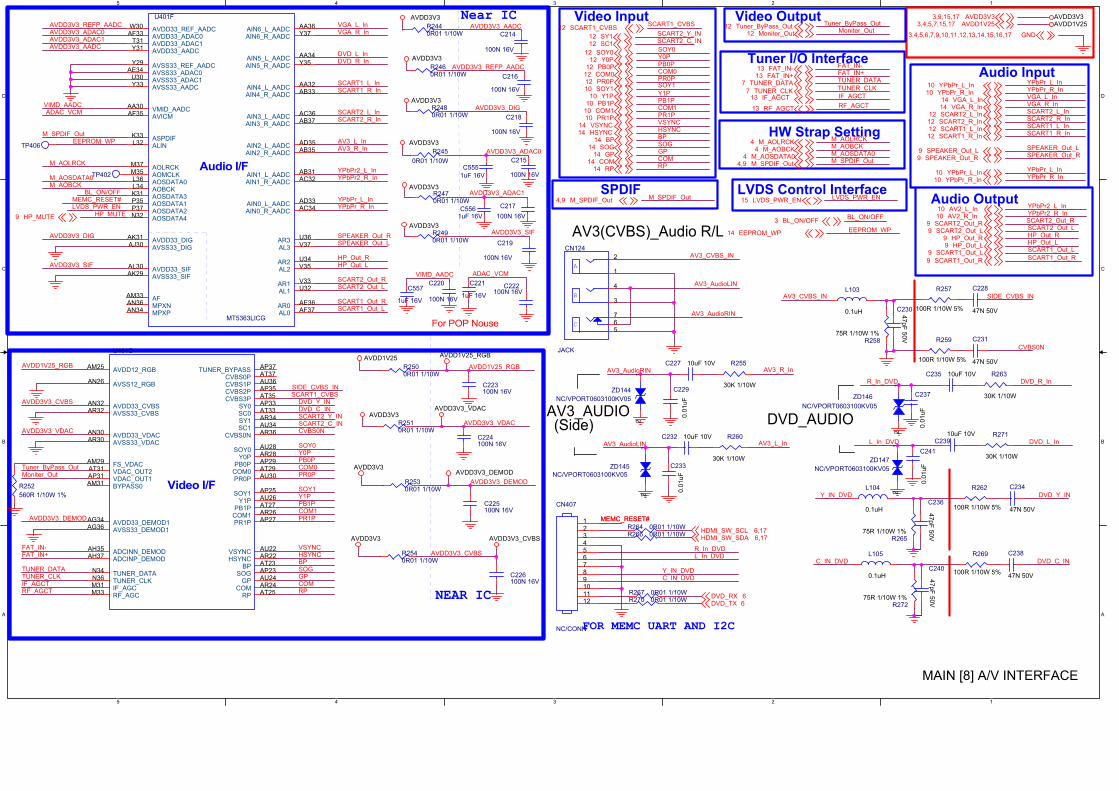
MAIN [8] A/V INTERFACE
5
5
4
4
3
3
2
2
1
1
D D
C C
B B
A A
PreAmp output for SCART2 Out
Audio Output
Pre-Amp Audio Output
Mute Control
Audio Mute Control
SPDIF
MT5363
OPTICALSPDIF OUT
HEADPHONE DRIVER
PreAmp output for Headphone
0.7VRMSPreAmp output for SCART1 Out
MT5363
MT5363
MT5363
HP_Out_LHP_Out_R
SCART2_Out_LSCART2_Out_RSCART1_Out_LSCART1_Out_R
SCART1L_PASCART1R_PA
SCART2L_PASCART2R_PA
HP_DET#
M_SPDIF_Out
HP_MUTE
A_MUTE
HP_MUTE
SCART2L_PA
AC_MUTE
SCART2R_PA
HPOUT_RT
HPOUT_LTHP_DET#
HPOUT_RT
SCART1R_PA
AC_MUTE
AC_MUTE
A_MUTE
M_SPDIF_Out
SCART2_Out_R
SCART2_Out_L
SCART1_Out_R_R
SCART1_Out_L_L
SCART1_Out_L
SCART1_Out_L_L
SCART1_Out_R_R
SCART1_Out_R
HPOUT_LT
GA0 GA1
HP_MUTE_OUT
GA1
GA0 A_MUTEHP_MUTE_OUT
SCART1L_PA
HP_MUTE
DVDD3V33,4,5,6,7,17AVDD3V33,8,15,17
GND3,4,5,6,7,8,10,11,12,13,14,15,16,17
SCART1_Out_R8SCART1_Out_L8SCART2_Out_R8SCART2_Out_L8
HP_Out_L8HP_Out_R8
SCART1R_PA12SCART1L_PA12SCART2R_PA12SCART2L_PA12
HP_DET#7
M_SPDIF_Out4,8
HP_MUTE8
A_MUTE11
HP_MUTE8
SPEAKER_Out_L8
SPEAKER_Out_R8
HP_Out_L8
HP_Out_R8
SPEAKER_L 11
SPEAKER_R 11
DVDD3V3AVDD3V3
DVDD3V3
AVDD3V3
AVDD3V3
AVDD3V3
AVDD3V3
AVDD3V3
AVDD3V3
AVDD3V3
AVDD3V3
C281 2.2uF 10VR699
NC
/10K
1/1
0W
C262
0.1uF 50V
C2790.1uF 50V
C520
10uF 10V
C2701uF 25V
R30410K 1/10W
R311NC/10K 1/10W
C256
10uF 10V
R2950R01 1/10W
L106
0.1uH
R574
0R01 1/10W
R748
NC/1K 1/10W
R63747K 1/10W
C265
0.1uF 50V
R739
NC/0R01 1/10W
D110
BAV70 3
1
2
R743
22R 1/10W 5%
R300 33R 1/10W 5%
C2762200pF 50V
R283
6.81K +-% 1/10W
C255
10uF 10VC517
10uF 10V
C271
10uF 10V
C26110uF 10V
C272
220P 50V
Q112
BC847C
R289
5.1K 1/10W
R309NC
R28747K 1/10W
R750
10K 1/10W
U606
TPA6132A2RTER
1
3
2
16
12
86
4
5
11
9
13
15
14
10
7
17
INL-
INR+
INL+
OU
TL
HPVDD
HP
VS
S
G0
INR-
OU
TR
CPP
CPN
EN
SG
ND
AV
DD
PGND
G1
Therm
al P
ad
CN603
CONNNECTOR
123
GNDVCCVIN
C523
2.2nF 25V
R288
6.81K +-% 1/10W
C282
2.2uF 10V
R290
6.81K +-% 1/10W
C549
10N 50V
R74422R 1/10W 5%
C273
10uF 10V
R708
47K 1/10W
C2861uF 16VR639
0R01 1/10W
U605
DRV602PW
1 212
11
96543
14
7810
13
+IN
R-I
NR
OU
TL
NC
PV
DD
PV
SS
EN
SG
ND
OU
TR
+IN
L
CN
CP
PG
ND
-IN
L
R716
NC/0R05OHM1/16W
R700
NC/10K 1/10W
R633
47K 1/10W
R28547K 1/10W
C259
2200pF 50V
C2772200pF 50V
C521
10uF 10V
R293
6.81K +-% 1/10WR294
5.1K 1/10W
R634
47K 1/10WC524
2.2nF 25V
R312
0R01 1/10W
C522
10uF 10V R701
NC
/10K
1/1
0W
C258
220P 50V
C274
220P 50V
C254
220P 50V
C285 1uF 25V
C518
10uF 10V
R282 27K 1/10W
U604
DRV602PW
1 212
11
96543
14
7810
13
+IN
R-I
NR
OU
TL
NC
PV
DD
PV
SS
EN
SG
ND
OU
TR
+IN
L
CN
CP
PG
ND
-IN
L
C519
10uF 10V
C257
10uF 10V
R306
100R 1/10W 5%
R29947K 1/10W
R284
5.1K 1/10W
C284 1uF 25V
R291
5.1K 1/10W
C2642200pF 50V
C2681uF 25V
R718
NC/0R05OHM1/16W
R698
NC/10K 1/10W
R292
0R01 1/10W
R709
47K 1/10W
R737
10K 1/10W
CN127
PHONEJACK
1762345
C2671uF 25V
C548
10N 50V
R7170R05OHM1/16W
R635
47K 1/10W
R27710K 1/10W
R738
0R05OHM1/16W
R73610K 1/10W
R27610K 1/10W
R296
27K 1/10W
R669 0R05OHM1/16W
C554
10uF 10V
R636
47K 1/10W
R29847K 1/10W
C269
10uF 10V
R286 27K 1/10W
R7190R05OHM1/16W
R668 0R05OHM1/16W
C266
1uF 25V
C283
1uF 16V
C275
10uF 10V
Q135BC847C
R29727K 1/10W
C260
10uF 10V
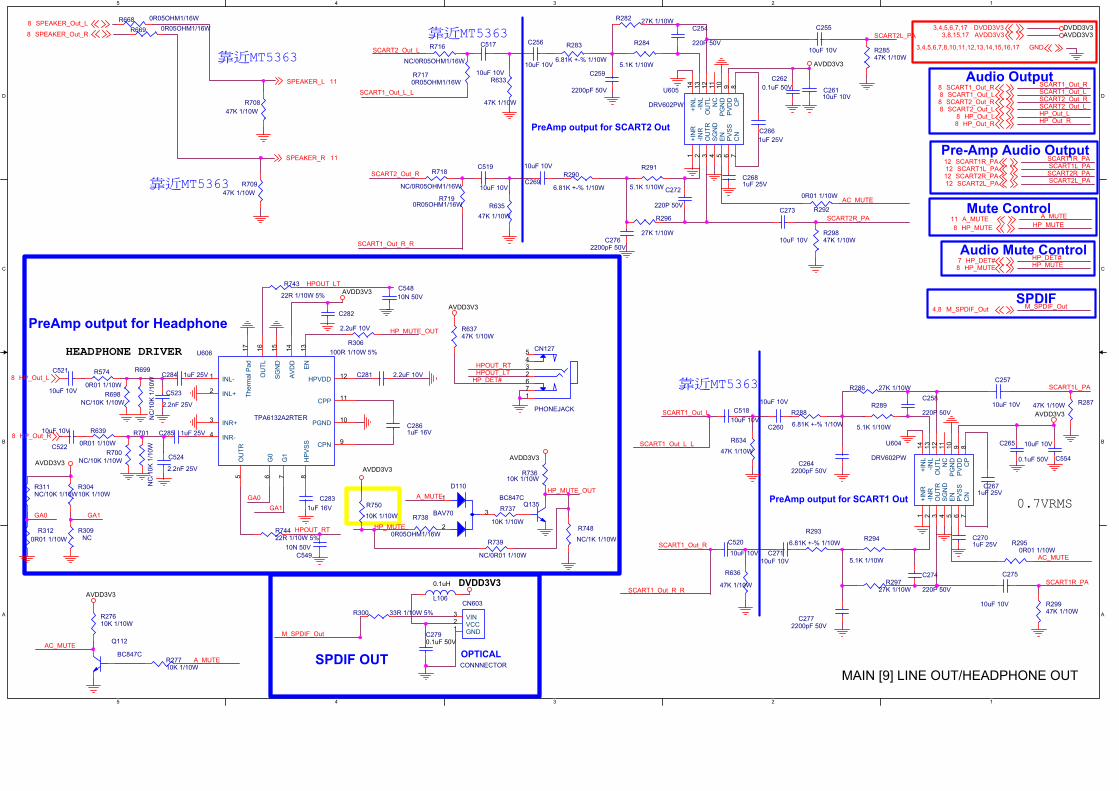
MAIN [9] LINE OUT/HEADPHONE OUT
5
5
4
4
3
3
2
2
1
1
D D
C C
B B
A A
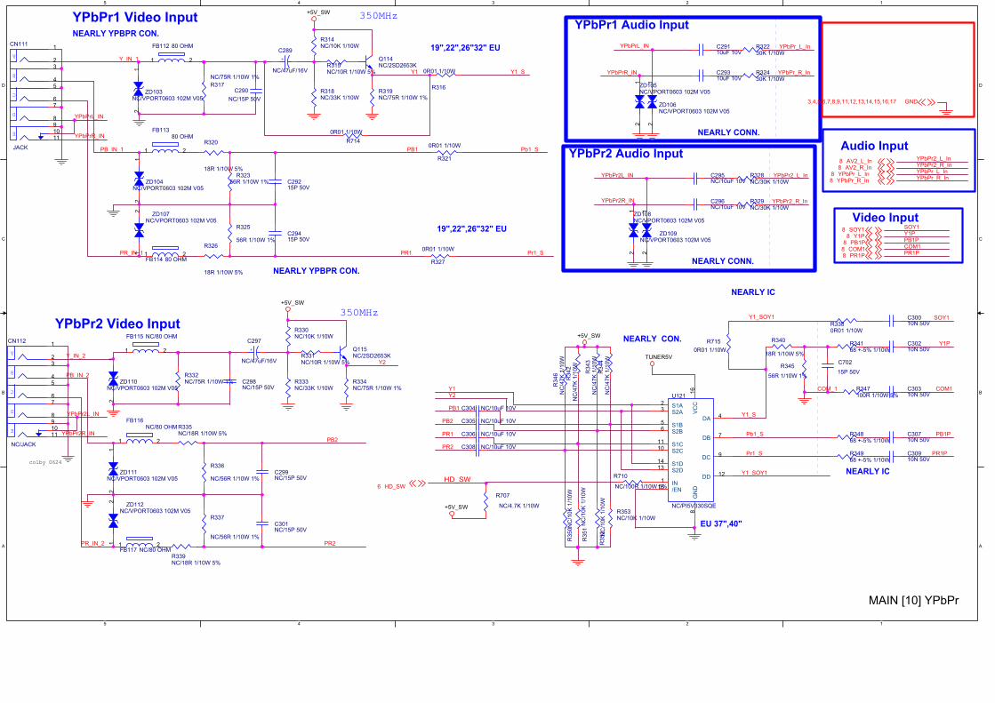
NEARLY YPBPR CON.
YPbPr1 Video Input
19",22",26"32" EU
19",22",26"32" EU
350MHz
NEARLY YPBPR CON.
YPbPr2 Video Input350MHz
YPbPr1 Audio Input
NEARLY CONN.
NEARLY CONN.
YPbPr2 Audio InputAudio Input
Video Input
NEARLY IC
EU 37",40"
NEARLY CON.
NEARLY IC
colby 0624
Pb1_S
Pr1_S
PB1
PR1
Y2
PB2
PR2
YPbPr_L_In
YPbPr2_R_In
YPbPr_R_In
YPbPr2_L_In
YPbPr2_R_InYPbPr_L_In
YPbPr2_L_In
YPbPr_R_In
COM1PB1PY1PSOY1
PR1P
Pr1_S
Y2
PB1P
Y1P
PB2
SOY1
COM1Y1
Pb1_S
PR1PPR2
PB1
PR1
PB_IN_2
YPbPr2L_IN
YPbPr2R_IN
Y_IN_2
YPbPr2R_IN
PR_IN_2
YPbPr2L_IN
HD_SW
Y_IN_1
COM_1
YPbPrR_IN
YPbPrL_IN
YPbPrR_IN
PB_IN_1
YPbPrL_IN
PR_IN_1
Y1_SOY1
Y1_S
Y1_SOY1
Y1 Y1_S
GND3,4,5,6,7,8,9,11,12,13,14,15,16,17
AV2_L_In8
YPbPr_R_In8YPbPr_L_In8
AV2_R_In8
PR1P8COM18PB1P8
Y1P8SOY18
HD_SW6
+5V_SW
+5V_SW
+5V_SW
TUNER5V
+5V_SW
U121
NC/PI5V330SQE
9
13
2
1
5
3
6
1110
12
14
15
4
16
8
7
DC
S2D
S1A
IN
S1B
S2A
S2B
S1CS2C
DD
S1D
/EN
DA
VC
CG
ND
DB
ZD111NC/VPORT0603 102M V05
12
ZD108NC/VPORT0603 102M V05
12
ZD106NC/VPORT0603 102M V05
12
ZD103NC/VPORT0603 102M V05
12
R332NC/75R 1/10W 1% C298
NC/15P 50V
R315NC/10R 1/10W 5%
R319NC/75R 1/10W 1%
R343
NC
/47K
1/1
0W
R330NC/10K 1/10W
R321
0R01 1/10W
ZD105NC/VPORT0603 102M V05
12
R715
0R01 1/10W
C29415P 50V
Q114NC/2SD2653K
C308 NC/10uF 10V
R331NC/10R 1/10W 5%
R34168 +-5% 1/10W
R335NC/18R 1/10W 5%
C702
15P 50V
R34968 +-5% 1/10W
FB116NC/80 OHM
1 2
R340
18R 1/10W 5%
R333NC/33K 1/10W
FB114 80 OHM1 2
R320
18R 1/10W 5%
R337
NC/56R 1/10W 1%
E
A
B
C
D
CN112
NC/JACK
1
23
45
67
891011
+
C289
NC/47uF/16V
R3380R01 1/10W
R351
NC
/10K
1/1
0W
R32230K 1/10W
R34868 +-5% 1/10W
R317
NC/75R 1/10W 1%
C290
NC/15P 50V
ZD107NC/VPORT0603 102M V05
12
R345
56R 1/10W 1%
C306 NC/10uF 10V
Q115NC/2SD2653K
C30010N 50V
R339NC/18R 1/10W 5%
R314NC/10K 1/10W
C299NC/15P 50V
R318NC/33K 1/10W
R326
18R 1/10W 5%
R714
0R01 1/10W
R334NC/75R 1/10W 1%
R344
NC
/47K
1/1
0W
R329NC/30K 1/10W
FB11380 OHM
1 2
C29110uF 10V
R325
56R 1/10W 1%
C304 NC/10uF 10V
R316
0R01 1/10W
R353NC/10K 1/10W
R342
NC
/47K
1/1
0W
R32356R 1/10W 1%
C30910N 50V
R350N
C/1
0K
1/1
0W
R710
NC/100R 1/10W 5%
R346
NC
/47K
1/1
0W
C29215P 50V
FB115 NC/80 OHM
1 2
FB117 NC/80 OHM1 2
C296NC/10uF 10V
C301NC/15P 50V
R707
NC/4.7K 1/10W
+
C297
NC/47uF/16V
C305 NC/10uF 10V
C30310N 50V
ZD112NC/VPORT0603 102M V05
12
FB112 80 OHM
1 2
C295NC/10uF 10V
R327
0R01 1/10W
ZD104NC/VPORT0603 102M V05
12
R347100R 1/10W 5%
R32430K 1/10W
R336
NC/56R 1/10W 1%
ZD110NC/VPORT0603 102M V05
12
R352 NC
/10K
1/1
0W
C30210N 50V
C29310uF 10V
E
A
B
C
D
CN111
JACK
1
23
45
67
891011
C30710N 50V
R328NC/30K 1/10W
ZD109NC/VPORT0603 102M V05
12
MAIN [10] YPbPr
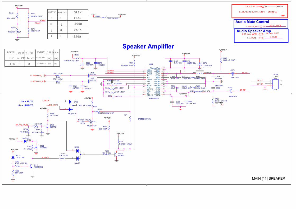
A
A
A A
0
32dB
0 20dB
AGAIN1
Audio Speaker Amp
14dB
0
Audio Mute Control1
-
11
Speaker Amplifier
+
+
-
AGAIN0
26dB
GAIN
1
0
HI = > UN-MUTE
LO = > MUTE
4N7
NC
0
R686
BD5444EFV
BD5445EFV
POWER
4N7
C693R688
0
6.2K
U602 C692
5W NC6.2K
10W
AGAIN0
SP_LP
SP_RP
A_MUTE
AGAIN1
AUDIO_MUTE
SP_LPAGAIN1AGAIN0
SP_Amp_MUTE
A_MUTE
AUDIO_MUTE
A_MUTE
SP_Amp_MUTE
SP_RP
A_MUTE9
+5VSB3,6,14,16,17
AUDIO_MUTE7
SPEAKER_L9
SPEAKER_R9
SP_Amp_MUTE6
GND3,4,5,6,7,8,9,10,12,13,14,15,16,17
PWRAMP
+5VSB
+24V
PWRAMPPWRAMP
PWRAMP
+5VSB
+5V_SW
+5VSB
+5VSB
+5VSB
PWRAMP
PWRAMP
PWRAMP
PWRAMP
PWRAMP
R36210K 1/10W
C572100N 50V
C693
4N7 50V
R72915K 1/10W
C5764.7uF 25V
R740390K +-5 1/10W
+ C57110uF/50V
+
C581 100uF25V
R3640R05 4A 1/4W
R354
NC/100K 1/10W
C5892.2uF 25V
C6924N7 50V
D109
NC/BAV70
3
1
2
+
C574
680uF 25V
Q116BC847C
R363470R 1/10W 1%
R727
20K 1/10W
C577330pF 50V
R741390K +-5 1/10W
+
C587
680uF 25V
R711
0R05OHM1/16W
R3710R01 1/10W
R370
NC/0R01 1/10W
D103
BAV70
3
1
2
C5701000PF 50V
R361
1K 1/10W
C5844.7uF 25V
L121 22uH 10%
R36010K 1/10W
R691 0R01 1/10W
R726
NC/0R05OHM1/16W
C5692.2uF 25V
C5901000PF 50V
R366
10K 1/10W
R746
1K 1/10W
R728
NC/10K 1/10W
R697
NC/100K 1/10W
Q117MMBT3904
C585330pF 50V C586
330N 50V
R68715 OHM 1/4W
L120 22uH 10%
R690 22K 1/10W
+ C573
470UF35V
CN128
CONN
1234
C588 10uF 10V
R686
0R01 1/10W
Q132
NC/BC847C
R367
NC/10K 1/10W
R36510K 1/10W
Q133BC847C
C5751uF 25V
D102BAS316
U602
BD5444EFV
123456789
1011121314 15
1617181920212223242526272829
VCCAGAIN0GAIN1IN1IN2GNDAFILAFILPROSCPDXMUTEXOSCMSREG_G VCCP2
VCCP2OUT2OUT2BSP2
GNDP2GNDP2GNDP1GNDP1
BSP1OUT1OUT1
VCCP1VCCP1
Thermal Pad
C5791uF 25V
C578
330N 50V
R745
NC/10K 1/10W
R68915 OHM 1/4W
R725NC/10K 1/10W
R688
0R01 1/10WC580 1uF 25V
+ C32247UF25V
R685
10OHM +-5% 1/8W
ZD113PDZ3.9B
12
R730
10K 1/10W
MAIN [11] SPEAKER
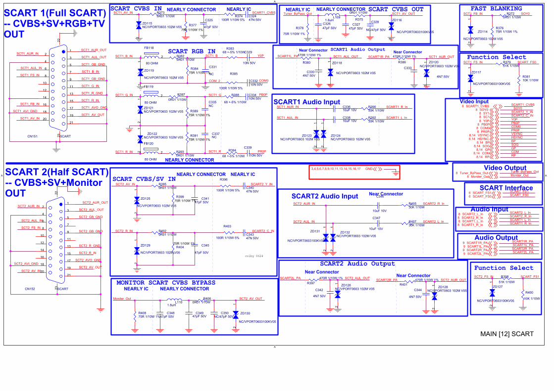
A
A
A A
Video Input
Audio Input
Video Output
Audio Output
SCART Interface
NEARLY ICNEARLY CONNECTORSCART 1(Full SCART)-- CVBS+SV+RGB+TVOUT
FAST BLANKING
Function Select
NEARLY CONNECTORNEARLY IC
SCART 2(Half SCART)-- CVBS+SV+MonitorOUT
NEARLY IC NEARLY CONNECTOR
MONITOR SCART CVBS BYPASS
NEARLY ICNEARLY CONNECTOR
Near Connector SCART1 Audio Output
SCART CVBS IN SCART CVBS OUT
SCART CVBS/SV IN
NEARLY CONNECTOR
SCART RGB IN Near Connector
colby 0624
SCART1 Audio Input
SCART2 Audio Input Near Connector
Near ConnectorNear Connector
SCART2 Audio OutputFunction Select
Moniter_OutTuner_ByPass_Out
BP
COM0
GP
PR0P
COM
VSYNC
RP
Y0P
HSYNC
PB0P
SOG
SCART1_L_InSCART1_R_In
SCART2_L_InSCART2_R_In
SCART_FS1SCART_FS0
Tuner_ByPass_Out
SCART_FS0
Moniter_Out SCT2_AV_OUT
SCART1L_PASCART1R_PA
SCART2L_PASCART2R_PA
SCT2_AUL_IN
SCT2_AUR_IN
SCT2_R_IN
SCT2_AV_OUT
SCT2_AUR_OUT
SCT2_AUL_OUT
SCT2_AV_IN
SCT2_FS_IN
SCART1_CVBS
SCART1_CVBS
SCART2_C_INSCART2_Y_IN
SOY0
SOY0
SCT1_BSCT1_B_IN
SCT1_R
COM0
PR0P
PB0P
Y0P
SCT1_G
SCART1R_PASCART1L_PA
SCART2_Y_IN
SCT2_R_IN
SCT2_AV_IN
SCART2_C_IN
SCART1_R_InSCT1_AUR_IN
SCART1_L_InSCT1_AUL_IN
SCART2_L_In
SCT2_AUR_IN
SCT2_AUL_IN
SCART2_R_In
SCART2L_PASCART2R_PA
SCT2_AUL_OUTSCT2_AUR_OUT
SCART_FS1
SCT1_G_IN
COM_2
SCT2_AVI_GND
SCT2_R_GND
SCT2_FS_IN
SCT1_R_IN
SCT1_AV_OUT
SCT1_FS_IN
SCT1_AUR_INSCT1_AUL_OUT
SCT1_AV_IN SCT1_AV_OUT
SCT1_AVO_GND
SCT1_B_IN
SCT1_AUR_OUT
SCT1_FB_IN
SCT1_FB_IN
SCT2_AVO_GND
SCT1_GB_GND
SCT1_AUR_OUT
SCT1_AVI_GND
SCT1_FS_IN
SCT1_G_IN
SCT1_GB_GND
SCT2_GB_GND
SCT2_GB_GND
SCT1_R_IN
SCT1_AV_IN
SCT1_R_GND
SCT1_AUL_IN
SCT1_AUL_OUT
Y0P8PB0P8
COM08PR0P8
VSYNC8,14HSYNC8,14
BP8,14SOG8,14
GP8,14COM8,14
RP8,14
Tuner_ByPass_Out8Moniter_Out8
SCART2_R_In8SCART1_L_In8SCART1_R_In8
SCART2_L_In8
SCART_FS16SCART_FS06
SCART1R_PA9SCART1L_PA9SCART2R_PA9SCART2L_PA9
SCART1_CVBS8
SC18SY18
SOY08
GND3,4,5,6,7,8,9,10,11,13,14,15,16,17
R386
470R 1/10W 1%
R39030K 1/10W
ZD119
NC/VPORT0603 102M V05
12
R388
68 +-5% 1/10W
ZD131
NC/VPORT0603100KV05
12
C339
10N 50V
ZD123NC/VPORT0603 102M V05
12
R40530K 1/10W
R37675R 1/10W 1%
C327
47pF 50V
R375
0R01 1/10W
R398
51K 1/10W
C325
47pF 50V
R389
75R 1/10W 1%
R396
100R 1/10W 5%
C342
4N7 50V
ZD116
NC/VPORT0603100KV05
12
C344
4N7 50V
ZD126NC/VPORT0603 102M V05
12
FB120
80 OHM
1 2
R401
470R 1/10W 1%
R38110K 1/10W
R400
10K 1/10W
R374100R 1/10W 5%
C331
NC
C333
4N7 50V
R399
75R 1/10W 1%
ZD122NC/VPORT0603 102M V05
12
C33810uF 10V
ZD118
NC/VPORT0603 102M V05
12
ZD127
NC/VPORT0603100KV05
12
ZD124NC/VPORT0603 102M V05
12
FB119
80 OHM
1 2
R3930R01 1/10W
C34047N 50V
R38368 +-5% 1/10W
R3820R01 1/10W
C34947pF 50V
ZD128NC/VPORT0603 102M V05
12
C34847pF 50V
R40875R 1/10W 1%
C33210N 50V
C346
10uF 10V
C337NC
L1101.8uH
C3304N7 50V
R403
100R 1/10W 5%
R40730K 1/10W
R397
470R 1/10W 1%
R378
75R 1/10W 1%
C33410N 50V
R384
75R 1/10W 1%
ZD114
NC/VPORT0603 102M V05
12
C335NC
C34147pF 50V
L1091.8uH
R4060R01 1/10W
R394
68 +-5% 1/10W
C32447N 50V
ZD121NC/VPORT0603 102M V05
12
C345
47pF 50V
R4020R01 1/10W
R37951K 1/10W
R39230K 1/10W
R377
75R 1/10W 1%
R391
75R 1/10W 1%
ZD125
NC/VPORT0603 102M V05
12
FB118
80 OHM
1 2
C350NC/47pF 50V
R3720R01 1/10W
C329
10N 50V
C34347N 50V
ZD115NC/VPORT0603 102M V05
12
R385
100R 1/10W 5%
R3950R01 1/10W
R387
0R01 1/10W
R40475R 1/10W 1%
ZD132NC/VPORT0603 102M V05
12
ZD120
NC/VPORT0603 102M V05
12
C33610uF 10V
ZD117
NC/VPORT0603100KV05
12
C326
47pF 50V
R380
470R 1/10W 1%
C347
10uF 10V
R3730R01 1/10W
CN151 SCART
12
34
56
78
910
1112
1314
1516
1718
1920
21
22
23
ZD129
NC/VPORT0603 102M V05
12
CN152 SCART
12
34
56
78
910
1112
1314
1516
1718
1920
21
22
23
ZD130
NC/VPORT0603100KV05
12
C328
NC/47pF 50V
MAIN [12] SCART
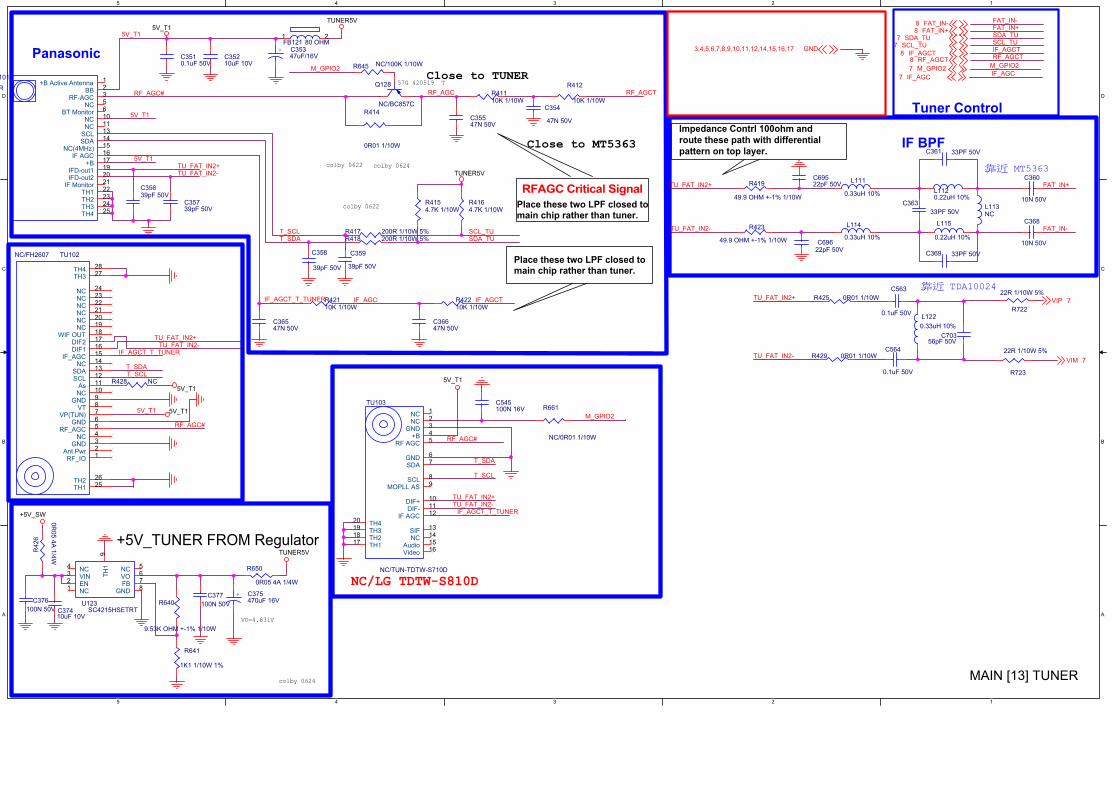
5
5
4
4
3
3
2
2
1
1
D D
C C
B B
A A
Panasonic
Impedance Contrl 100ohm and
route these path with differential
pattern on top layer.
Place these two LPF closed tomain chip rather than tuner.
IF BPFClose to MT5363
RFAGC Critical Signal
Place these two LPF closed tomain chip rather than tuner.
MT5363
+5V_TUNER FROM Regulator
colby 0622
57G 420519 T
colby 0622
Tuner Control
TDA10024
colby 0624
colby 0624
NC/LG TDTW-S810D
Close to TUNER
VO=4.831V
IF_AGC IF_AGCT
5V_T1
T_SCL
5V_T1
RF_AGC# RF_AGC
FAT_IN+
IF_AGCTRF_AGCT
SCL_TUSDA_TU
FAT_IN-
SDA_TUSCL_TU
RF_AGCT
M_GPIO2 M_GPIO2
T_SCL
5V_T1
T_SDA
IF_AGCT_T_TUNER
RF_AGC#
T_SCL
TU_FAT_IN2-TU_FAT_IN2+
T_SDA
RF_AGC#
5V_T1
T_SDA
TU_FAT_IN2-
TU_FAT_IN2-
TU_FAT_IN2+
M_GPIO2
FAT_IN+
FAT_IN-
TU_FAT_IN2+
TU_FAT_IN2+
TU_FAT_IN2-
TU_FAT_IN2+
TU_FAT_IN2-
IF_AGC
IF_AGCT_T_TUNER
IF_AGCT_T_TUNER
GND3,4,5,6,7,8,9,10,11,12,14,15,16,17
SDA_TU7SCL_TU7
RF_AGCT8
FAT_IN+8
IF_AGCT8
FAT_IN-8
M_GPIO27
IF_AGC7
VIM 7
VIP 7
TUNER5V
TUNER5V
5V_T1TUNER5V
+5V_SW
5V_T1
5V_T1
5V_T1
C564
0.1uF 50V
R428 NC
C359
39pF 50V
Q128
NC/BC857C
C36647N 50V
C363
33PF 50V
R640
9.53K OHM +-1% 1/10W
R414
0R01 1/10W
R4154.7K 1/10W
L114
0.33uH 10%
C368
10N 50V
U123SC4215HSETRT
1234
8765
9
NCENVINNC
GNDFBVONC
TH
1
C35639pF 50V
TU102NC/FH2607
2526
2728
1234567891011121314151617
1920212223
18
24
TH1TH2
TH3TH4
RF_IOAnt Pwr
GNDNC
RF_AGCGND
VP(TUN)VT
GNDNCAs
SCLSDA
NCIF_AGC
DIF1DIF2
NCNCNCNCNC
WIF OUT
NCR425 0R01 1/10W
L111
0.33uH 10% L1120.22uH 10%
C563
0.1uF 50V
R645 NC/100K 1/10W
R41110K 1/10W
R722
22R 1/10W 5%
R418 200R 1/10W 5%C696
22pF 50V
C35739pF 50V
C376
100N 50V
C369 33PF 50V
L122
0.33uH 10%
R423
49.9 OHM +-1% 1/10W
C70356pF 50V
R723
22R 1/10W 5%
R641
1K1 1/10W 1%
C354
47N 50V
+ C375470uF 16V
C377
100N 50V
R419
49.9 OHM +-1% 1/10W
C361 33PF 50V
C545100N 16V
C3510.1uF 50V
R426
0R
05 4
A 1
/4W
C69522pF 50V
C36547N 50V
101
R
1235610111314151617
22232425
192021
+B Active AntennaBB
RF-AGCNC
BT MonitorNCNC
SCLSDA
NC(4MHz)IF AGC
+B
TH1TH2TH3TH4
IFD-out1IFD-out2
IF Monitor
L115
0.22uH 10%
+ C35347uF/16V
C35547N 50V
C360
10N 50V
R650
0R05 4A 1/4W
FB121 80 OHM1 2
R429 0R01 1/10W
R42210K 1/10W
R42110K 1/10W
L113NC
R661
NC/0R01 1/10W
R412
10K 1/10W
C358
39pF 50V
TU103
NC/TUN-TDTW-S710D
12345
67
17181920
89
101112
13141516
NCNC
GND+B
RF AGC
GNDSDA
TH1TH2TH3TH4
SCLMOPLL AS
DIF+DIF-
IF AGC
SIFNC
AudioVideo
R417 200R 1/10W 5%
R4164.7K 1/10W
C37410uF 10V
C35210uF 10V
MAIN [13] TUNER
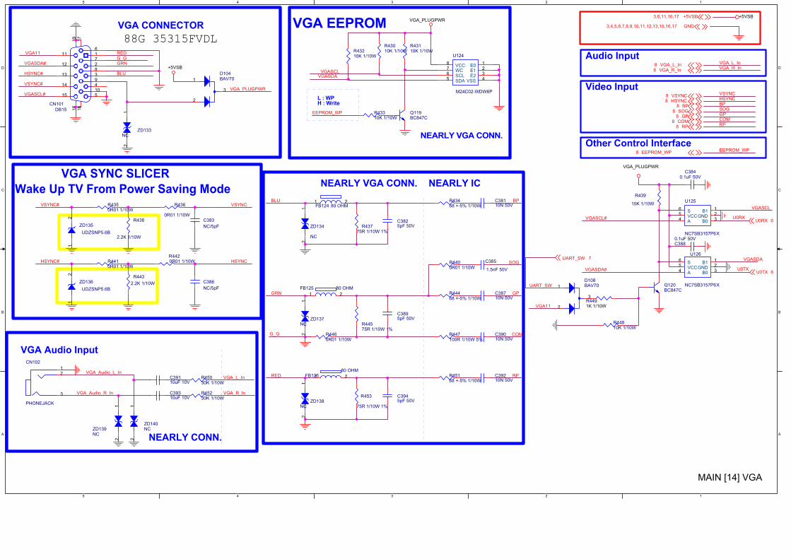
5
5
4
4
3
3
2
2
1
1
D D
C C
B B
A A
NEARLY VGA CONN.
Video Input
Wake Up TV From Power Saving Mode
VGA SYNC SLICER
Audio Input
VGA Audio Input
H : Write
NEARLY CONN.
NEARLY VGA CONN.
Other Control Interface
NEARLY IC
L : WP
VGA EEPROM88G 35315FVDL
VGA CONNECTOR
VGA_R_In
VGA_L_In
COM
EEPROM_WP
VSYNC
COM
VGA_R_In
RP
BP
SOG
RP
BP
VGA_L_In
HSYNC
EEPROM_WP GP
GP
SOG
HSYNC#
VGASCLVGASDA
VGA_Audio_R_In
VGA_Audio_L_InRED
GRN
VSYNC
HSYNC
VGASCL
U0RX
VGASDA
VGASDA#
VGASCL#
U0TX
UART_SW
VGA11
BLU
VSYNC#
RED
VGASDA#G_G
VGASCL#VGA_PLUGPWR
GRN
BLUHSYNC#
VGA11
G_G
VSYNC#
GND3,4,5,6,7,8,9,10,11,12,13,15,16,17
SOG8
+5VSB3,6,11,16,17
VGA_L_In8
GP8COM8
VGA_R_In8
VSYNC8
EEPROM_WP8
RP8
HSYNC8BP8
U0TX 6
U0RX 6
UART_SW 7
VGA_PLUGPWR+5VSB
VGA_PLUGPWR
+5VSB
R4460R01 1/10W
ZD138NC
12
C3880.1uF 50V
R43210K 1/10W
R45030K 1/10W
D104BAV70
3
1
2
C39210N 50V
R43310K 1/10W
ZD135
UDZSNP5.6B
12
R44810K 1/10W
R45168 +-5% 1/10W
U125
NC7SB3157P6X
1234
56 B1
GNDB0A
VCCS
R436
0R01 1/10WR438
2.2K 1/10W
Q120BC847C
R44575R 1/10W 1%
R4420R01 1/10W
ZD136
UDZSNP5.6B
12
R447100R 1/10W 5%
R4350R01 1/10W
CN101
DB15
16
27
38
49
5
11
12
13
14
1510
17
16
18
19
R4410R01 1/10W
C38110N 50V
R43468 +-5% 1/10W
C386
NC/5pF
ZD133NC
12
C39010N 50V
C3825pF 50V
D108BAV70
3
1
2
Q119BC847C
ZD139NC
12
C3840.1uF 50V
R43110K 1/10W
C39310uF 10V C394
5pF 50V
C385
1.5nF 50V
R453
75R 1/10W 1%
R4400R01 1/10W
R43775R 1/10W 1%
C38710N 50V
C383
NC/5pF ZD134
NC
12
FB12680 OHM
1 2
R43010K 1/10W
FB125 80 OHM
1 2
R443
2.2K 1/10W
FB124 80 OHM1 2
U124
M24C02-WDW6P
12345
678 E0
E1E2
VSSSDASCLWCVCC
ZD137NC
12
R439
10K 1/10W
R4491K 1/10W
U126
NC7SB3157P6X
1234
56 B1
GNDB0A
VCCS
C3895pF 50V
CN102
PHONEJACK
12
3
C39110uF 10V
R44468 +-5% 1/10W
R45230K 1/10W
ZD140NC
12
MAIN [14] VGA
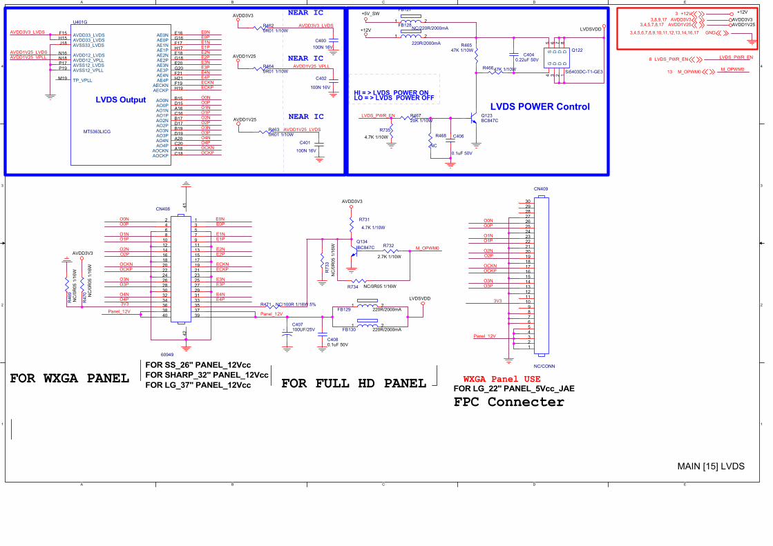
A
A
B
B
C
C
D
D
E
E
4 4
3 3
2 2
1 1
NEAR IC
NEAR IC
NEAR IC
HI = > LVDS POWER ON
LVDS POWER ControlLO = > LVDS POWER OFF
WXGA Panel USE
FOR SS_26" PANEL_12Vcc
FOR LG_22" PANEL_5Vcc_JAE
FOR SHARP_32" PANEL_12VccFOR WXGA PANELFOR LG_37" PANEL_12Vcc FOR FULL HD PANEL
FPC Connecter
LVDS_PWR_EN
AVDD3V3_LVDS
AVDD1V25_VPLL
AVDD1V25_LVDS
O1N
O3P
E0P
ECKN
O2NO1P
OCKN
E0N
O4N
ECKP
OCKP
O2P
E1N
AVDD3V3_LVDS
E2P
E4N
AVDD1V25_VPLLE2NE1P
O4P
E3N
O0N
AVDD1V25_LVDS
E4P
O0P
E3P
O3N
LVDS_PWR_EN
O1N
O0P
E3P
E1P
E0P
E3N
OCKPOCKN
O3N
E2N
O0N
O2N
ECKP
O2P
O1N
O0PE0N
O2N
E4N
E1N
E2P
O1P
O0N
OCKN
3V3
O3P
OCKP
O1P
O3N
ECKN
O2P
Panel_12V
O4N
Panel_12V
O4P
Panel_12V
E4P
O3P
3V3
M_OPWM0
M_OPWM0
AVDD3V33,8,9,17AVDD1V253,4,5,7,8,17
GND3,4,5,6,7,8,9,10,11,12,13,14,16,17
+12V3
LVDS_PWR_EN8
M_OPWM013
+12V
AVDD3V3AVDD1V25
AVDD3V3
AVDD1V25
AVDD1V25
+12V
+5V_SW
LVDSVDD
LVDSVDD
AVDD3V3
AVDD3V3
C406
0.1uF 50V
C401
100N 16V
CN408
60949
2468
10121416182022242628303234363840
13579111315171921232527293133353739
41
42
+
C407100UF/25V
R735
4.7K 1/10W
FB128
220R/2000mA
1 2
C4080.1uF 50V
FB129 220R/2000mA1 2
R470
NC
/0R
05 1
/16W
C402
100N 16V
R46647K 1/10W
R733
NC
/0R
05 1
/16W
R734 NC/0R05 1/16W
R4630R01 1/10W
CN409
NC/CONN
123456789
101112131415161718192021222324252627282930
R46720K 1/10W
C400
100N 16V
FB130 220R/2000mA1 2
R46547K 1/10W
R4620R01 1/10W
R4640R01 1/10W
Q134
BC847C R732
2.7K 1/10W
R468
NC
Q122
Si5403DC-T1-GE3
12345 6 7 8
DDDGS D D D
C4040.22uF 50V
R471 NC/100R 1/16W 5%
LVDS Output
U401G
MT5363LICG
E16
J18
D15B15
G16F17
N16
C16A16
H17
F15
P17
D17B17
G18E18
H15
N18
C18A18
H19F19
P19
D19B19
G20E20
C20A20
H21F21
M19
AE0N
AVSS33_LVDS
AO0PAO0N
AE0PAE1N
AVDD12_LVDS
AO1PAO1N
AE1P
AVDD33_LVDS
AVSS12_LVDS
AO2PAO2N
AE2PAE2N
AVDD33_LVDS
AVDD12_VPLL
AOCKPAOCKN
AECKPAECKN
AVSS12_VPLL
AO3PAO3N
AE3PAE3N
AO4PAO4N
AE4PAE4N
TP_VPLL
R469
NC
/0R
05 1
/16W
Q123BC847C
FB127
NC/220R/2000mA
1 2
R731
4.7K 1/10W
MAIN [15] LVDS
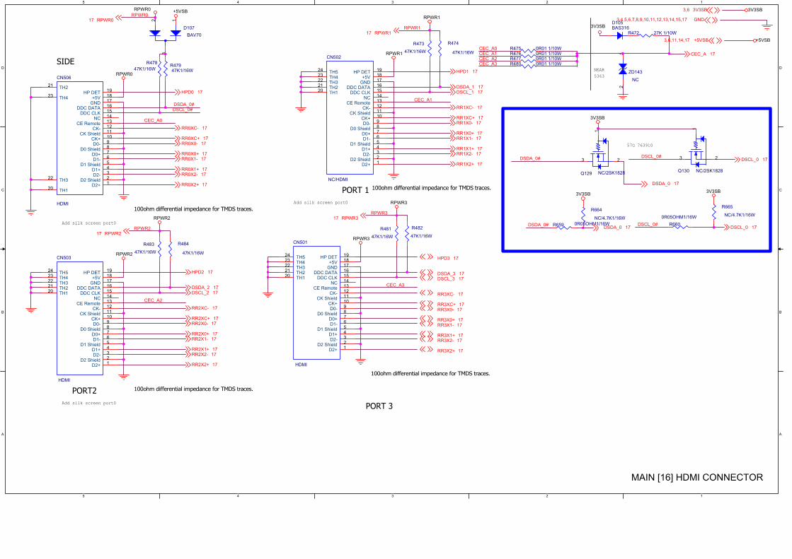
5
5
4
4
3
3
2
2
1
1
D D
C C
B B
A A
100ohm differential impedance for TMDS traces.
100ohm differential impedance for TMDS traces.
SIDE
PORT 3
100ohm differential impedance for TMDS traces.
PORT 1
Add silk screen port0
100ohm differential impedance for TMDS traces.
Add silk screen port0
Add silk screen port0
PORT2
NEAR
5363
57G 763910
CEC_A0
CEC_A2
CEC_A1
RPWR1
CEC_A3
RPWR2
CEC_A0
DSCL_0#
CEC_A2
RPWR3
CEC_A1
CEC_A3
DSCL_0#DSDA_0#
DSCL_0#
RPWR0
DSDA_0#
DSDA_0#
RR1XC- 17
RR0X0- 17
DSCL_1 17
RR3X2+ 17
RR1X1- 17
DSCL_3 17
RR3X0+ 17
DSCL_2 17
RR0X1+ 17
RR2X1- 17
RR2XC+ 17
DSDA_3 17
RR3X0- 17
RR1X1+ 17
HPD0 17
RR2X0+ 17
HPD2 17
RR0X2+ 17
RR3XC+ 17
RR2X2+ 17
RR1X0+ 17
RPWR317
RR1X0- 17
RR3X2- 17
CEC_A 17
RR2X2- 17
RR2XC- 17
RR3XC- 17
DSDA_2 17
RR1XC+ 17
HPD3 17
RR0X0+ 17
RR0X2- 17
RR3X1+ 17
RPWR117
RR0X1- 17
RR0XC- 17
RR3X1- 17
DSDA_1 17
HPD1 17
RR1X2+ 17
RR2X0- 17
RPWR217
RR0XC+ 17
RR1X2- 17
RR2X1+ 17
3V3SB3,6
GND3,4,5,6,7,8,9,10,11,12,13,14,15,17
DSDA_0 17
DSCL_0 17
DSDA_0 17 DSCL_0 17
RPWR017
+5VSB3,6,11,14,17
RPWR3
RPWR1
RPWR2
RPWR3
RPWR0
RPWR2
RPWR1
3V3SB
3V3SB
3V3SB
3V3SB3V3SB
RPWR0 +5VSB
+5VSB
R47947K1/16W
CN501
HDMI
2021
12345678910111213141516171819
222324
TH1TH2
D2+D2 Shield
D2-D1+
D1 ShieldD1-D0+
D0 ShieldD0-
CK+CK Shield
CK-CE Remote
NCDDC CLK
DDC DATAGND+5V
HP DET
TH3TH4TH5
R475 0R01 1/10W
D105BAS316
CN503
HDMI
2021
12345678910111213141516171819
222324
TH1TH2
D2+D2 Shield
D2-D1+
D1 ShieldD1-D0+
D0 ShieldD0-
CK+CK Shield
CK-CE Remote
NCDDC CLK
DDC DATAGND+5V
HP DET
TH3TH4TH5
R478
47K1/16W
D107
BAV70
3
12
R482
47K1/16W
R474
47K1/16W
R477 0R01 1/10W
R481
47K1/16W
R473
47K1/16W
R664
NC/4.7K1/16W
R476 0R01 1/10W
ZD143
NC
12
CN506
HDMI
20
21
12345678910111213141516171819
22
23
TH1
TH2
D2+D2 Shield
D2-D1+
D1 ShieldD1-D0+
D0 ShieldD0-
CK+CK Shield
CK-CE Remote
NCDDC CLK
DDC DATAGND+5V
HP DET
TH3
TH4
R472 27K 1/10W
R659 0R05OHM1/16W
R480 0R01 1/10W
R483
47K1/16W
R665
NC/4.7K1/16W
R484
47K1/16W
Q129 NC/2SK1828
3
1
2
CN502
NC/HDMI
2021
12345678910111213141516171819
222324
TH1TH2
D2+D2 Shield
D2-D1+
D1 ShieldD1-D0+
D0 ShieldD0-
CK+CK Shield
CK-CE Remote
NCDDC CLK
DDC DATAGND+5V
HP DET
TH3TH4TH5
Q130 NC/2SK1828
3
1
2
R660
0R05OHM1/16W
MAIN [16] HDMI CONNECTOR
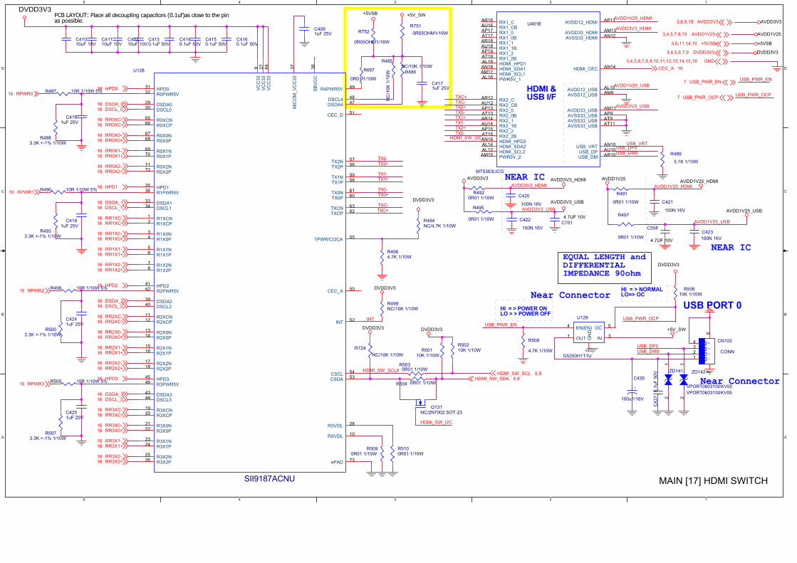
5
5
4
4
3
3
2
2
1
1
D D
C C
B B
A A
NEAR IC
PCB LAYOUT: Place all decoupling capacitors (0.1uf)as close to the pinas possible.
NEAR ICEQUAL LENGTH andDIFFERENTIALIMPEDANCE 90ohm
Near Connector
USB PORT 0
LO=> OC
LO = > POWER OFF
Near ConnectorHI = > NORMAL
HI = > POWER ON
AVDD1V25_HDMI
TX1-
USB_VRT
TX0-
USB_DP0
TX2+
AVDD3V3_HDMI
TX2-
TX0-TX0+
TXC+
AVDD3V3_HDMI
TXC-
USB_DM0
TX1+
TXC-
TX2-
INT
TX0+
TX2+
TXC+
AVDD1V25_HDMI
TX1+
TX1-
HDMI_SW_SCL#
AVDD3V3_USB
AVDD1V25_USB
AVDD3V3_USB
AVDD1V25_USB
HDMI_SW_I2C
HDMI_SW_I2C
USB_PWR_EN
USB_PWR_OCP
USB_DM0USB_DP0
USB_PWR_OCP
USB_PWR_EN
DSDA_116
RPWR016
RR2XC-16
RR1XC+16
DSDA_316
RR2X1-16
RR1X1-16
RR1X2+16RR1X2-16
RR2X1+16
DSCL_116
RR0XC+16
RR0X1+16
RR3X0+16
RPWR116
RR0X1-16
RR1X0-16
RR1X1+16
RR3X1-16
RR3X0-16
RR2X2+16
DSCL_216
RPWR216
RPWR316
RR3X2+16
RR2X0+16
RR0X0-16
RR3X1+16
RR1X0+16
RR2X2-16
RR1XC-16
RR0XC-16
RR0X2+16RR0X2-16
RR0X0+16
AVDD3V33,8,9,15
RR3X2-16
DSCL_016
HPD216
AVDD1V253,4,5,7,8,15
CEC_A 16
+5VSB3,6,11,14,16
HPD316
RR3XC+16
DVDD3V33,4,5,6,7,9
GND3,4,5,6,7,8,9,10,11,12,13,14,15,16
DSDA_216
DSCL_316
HDMI_SW_SCL 6,8
DSDA_016
HPD116
HPD016
RR3XC-16
RR2X0-16
RR2XC+16
HDMI_SW_SDA 6,8
USB_PWR_EN7
USB_PWR_OCP7
AVDD3V3_HDMI
AVDD3V3
AVDD3V3_USB
+5VSB
AVDD1V25_HDMIAVDD1V25
DVDD3V3
AVDD1V25
DVDD3V3
AVDD3V3
AVDD1V25_USB
DVDD3V3
DVDD3V3
DVDD3V3
DVDD3V3 +5V_SW
DVDD3V3
+5VSB +5V_SW
R4964.7K 1/10W
C4241uF 25V
R5100R01 1/10W
R751
0R05OHM1/16W
R504 0R01 1/10W
SII9187ACNU
U128
10
5354
6566
6768
6970
7172
6362
6160
5958
5756
73
9
1112
1314
1516
1718
29
50
3132
30
55
4748
4142
3940
51
3536
3334
12
34
56
78
27
64
52
37
4546
4344
1920
2122
2324
2526
38
28
49
RSVDL
CSDACSCL
R0XCNR0XCP
R0X0NR0X0P
R0X1NR0X1P
R0X2NR0X2P
TXCNTXCP
TX0NTX0P
TX1NTX1P
TX2NTX2P
ePAD
VC
C33
R2XCNR2XCP
R2X0NR2X0P
R2X1NR2X1P
R2X2NR2X2P
DSDA0
CEC_A
HPD0R0PWR5V
DSCL0
TPWR/CI2CA
DSDA4DSCL4
HPD2R2PWR5V
DSDA2DSCL2
CEC_D
HPD1R1PWR5V
DSDA1DSCL1
R1XCNR1XCP
R1X0NR1X0P
R1X1NR1X1P
R1X2NR1X2P
VC
C33
VC
C33
INT
MIC
OM
_V
CC
33
HPD3R3PWR5V
DSDA3DSCL3
R3XCNR3XCP
R3X0NR3X0P
R3X1NR3X1P
R3X2NR3X2P
SB
VC
C
RSVDL
R4PWR5V
C41110uF 10V
R505 10R 1/10W 5%
R50110K 1/10W
R724
NC/10K 1/10W
C4130.1uF 50V
C4091uF 25V
R485
NC
/10K
1/1
0W
C4160.1uF 50V
C701
4.7UF 10V
R5073.3K +-1% 1/10W
R4933.3K +-1% 1/10W
U129
G5250H1T1U
1
2
3
4 5
OUT GN
D
IN
EN(EN) OC
C420
100N 16V
R752
0R05OHM1/16W
R490 10R 1/10W 5%
HDMI &
USB I/F
U401E
MT5363LICG
AP11
AN12
AR12AU12
AM13
AP13AT13
AL12
AN14
AR14AU14AP15AT15
AR16AU16AP17AT17AR18AU18AP19AT19
AL14
AM15
AN16
AM17
AL18AN18
AM9AL10
AM11
AN10AU10AR10
AL16
AP9AT9AT11
AVDD12_HDMI
AVSS33_HDMI
RX2_CRX2_CB
AVDD33_HDMI
RX2_0RX2_0B
HDMI_SCL2
HDMI_CEC
RX2_1RX2_1BRX2_2RX2_2B
RX1_CRX1_CBRX1_0RX1_0BRX1_1RX1_1BRX1_2RX1_2B
HDMI_SDA2
PWR5V_2
HDMI_HPD2
HDMI_SCL1
HDMI_HPD1HDMI_SDA1
AVSS12_USBAVDD12_USB
AVDD33_USB
USB_VRTUSB_DPUSB_DM
PWR5V_1
AVSS33_USBAVSS33_USBAVSS33_USB
R499NC/10K 1/10W
R497
0R01 1/10W
C421
100N 16V
12
34 CN103
CONN
1234
65
R487 10R 1/10W 5%
R498 10R 1/10W 5% R50610K 1/10W
R50210K 1/10W
+
C426
100uF/16V
C4191uF 25V
R5003.3K +-1% 1/10W
R5030R01 1/10W
R494NC/4.7K 1/10W
R491
0R01 1/10W
C4150.1uF 50V
R508
4.7K 1/10W
Q131NC/2N7002 SOT-23
R486
NC/10K 1/10W
C558
4.7UF 10V
R489
5.1K 1/10W
R4920R01 1/10W
C4251uF 25V
ZD141
VPORT0603100KV05
12
C423
100N 16V
C427
0.1
uF
50V
C41010uF 10V
C422
100N 16V
C4171uF 25V
C4140.1uF 50V
R667
0R01 1/10W
R495
0R01 1/10W
C4181uF 25V
R4883.3K +-1% 1/10W
R5090R01 1/10W
ZD142
VPORT0603100KV05
12
C41210uF 10V
MAIN [17] HDMI SWITCH
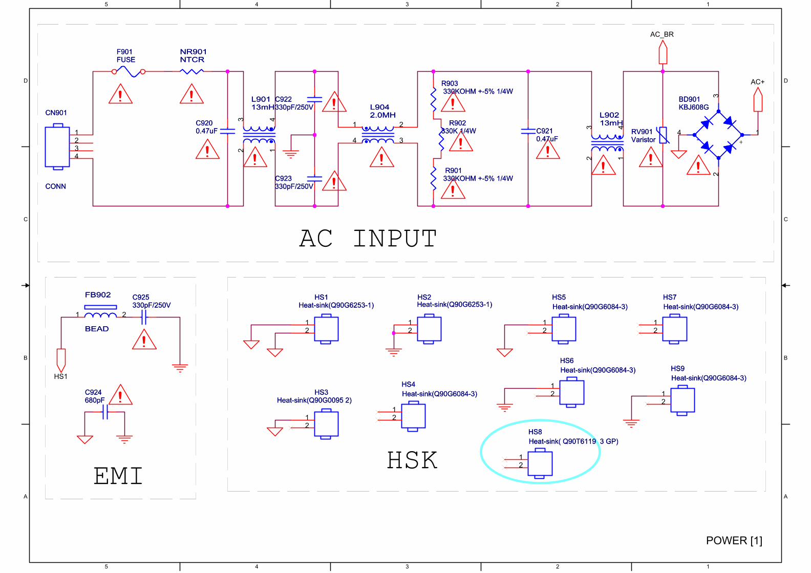
5
5
4
4
3
3
2
2
1
1
D D
C C
B B
A A
AC+
AC_BR
HS1
! !
!!
!
!
!
!
!
!
!
!!
!
!
!
AC INPUT
EMIHSK
HS1Heat-sink(Q90G6253-1)
HS1Heat-sink(Q90G6253-1)
12
C925330pF/250VC925330pF/250V
HS6
Heat-sink(Q90G6084-3)
HS6
Heat-sink(Q90G6084-3)
12HS3
Heat-sink(Q90G0095 2)HS3
Heat-sink(Q90G0095 2)
12
R902330K 1/4W
R902330K 1/4W RV901
VaristorRV901Varistor
HS4
Heat-sink(Q90G6084-3)
HS4
Heat-sink(Q90G6084-3)
12
C922330pF/250VC922330pF/250V
FB902
BEAD
FB902
BEAD
1 2
F901FUSEF901FUSE
HS8
Heat-sink( Q90T6119 3 GP)
HS8
Heat-sink( Q90T6119 3 GP)
12
L90213mHL90213mH
12
43
R901 330KOHM +-5% 1/4W
R901 330KOHM +-5% 1/4W
R903 330KOHM +-5% 1/4WR903 330KOHM +-5% 1/4W
C9210.47uFC9210.47uF
HS9
Heat-sink(Q90G6084-3)
HS9
Heat-sink(Q90G6084-3)
12
L9042.0MHL9042.0MH
1
4
2
3
-+
BD901KBJ608G
-+
BD901KBJ608G
2
1
3
4
NR901NTCRNR901NTCR
HS5
Heat-sink(Q90G6084-3)
HS5
Heat-sink(Q90G6084-3)
12
HS2 Heat-sink(Q90G6253-1)HS2
Heat-sink(Q90G6253-1)
12
C923330pF/250VC923330pF/250V
HS7
Heat-sink(Q90G6084-3)
HS7
Heat-sink(Q90G6084-3)
12
CN901
CONN
CN901
CONN
1234
C924680pFC924680pF
L90113mHL90113mH
12
43
C9200.47uFC9200.47uF
POWER [1]
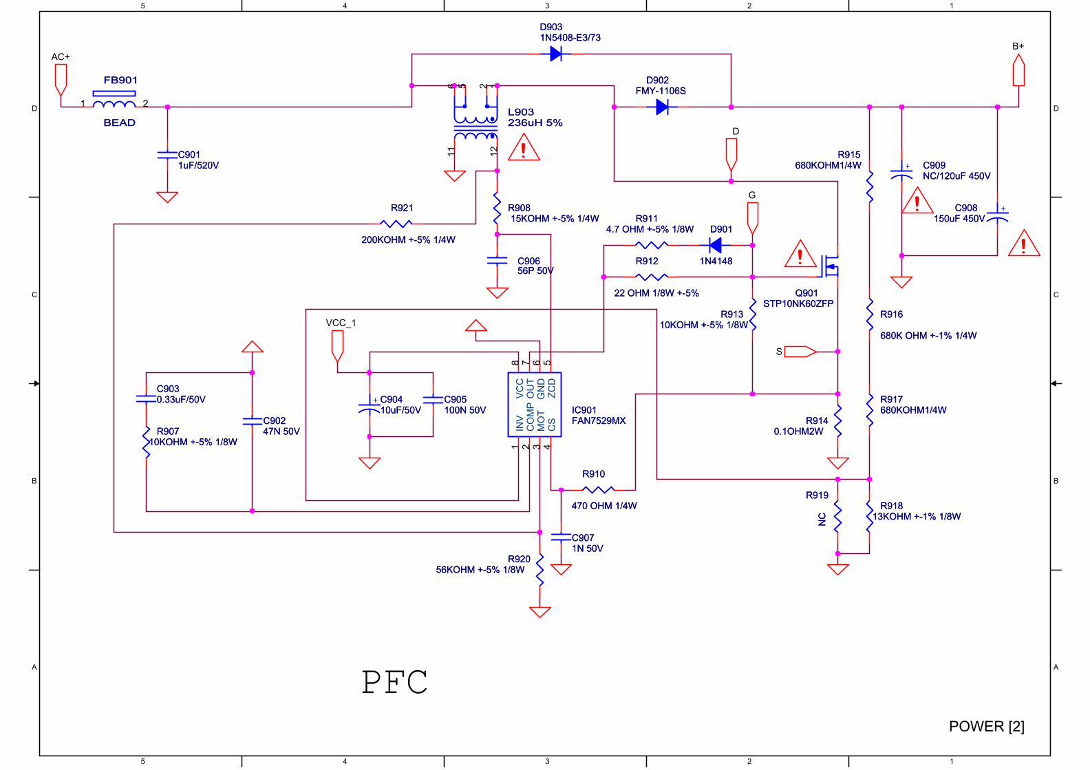
5
5
4
4
3
3
2
2
1
1
D D
C C
B B
A A
VCC_1
AC+B+
S
D
G
!
!
!
!
PFC
D901
1N4148
D901
1N4148
C9071N 50VC9071N 50V
R913 10KOHM +-5% 1/8W
R913 10KOHM +-5% 1/8W
R918 13KOHM +-1% 1/8W
R918 13KOHM +-1% 1/8W
R919
NC
R919
NC
IC901FAN7529MXIC901FAN7529MX
INV
1
CO
MP
2
MO
T3
CS
4Z
CD
5G
ND
6O
UT
7V
CC
8
C905100N 50VC905100N 50V
L903236uH 5%L903236uH 5%
11
12
56 2 1
FB901
BEAD
FB901
BEAD
1 2
R908 15KOHM +-5% 1/4WR908 15KOHM +-5% 1/4W
C90247N 50VC90247N 50V
R912
22 OHM 1/8W +-5%
R912
22 OHM 1/8W +-5%
+ C90410uF/50V
+ C90410uF/50V
C90656P 50VC90656P 50V
R920 56KOHM +-5% 1/8W
R920 56KOHM +-5% 1/8W
R907 10KOHM +-5% 1/8W
R907 10KOHM +-5% 1/8W
D9031N5408-E3/73D9031N5408-E3/73
+C908150uF 450V
+C908150uF 450V
R921
200KOHM +-5% 1/4W
R921
200KOHM +-5% 1/4W
C9030.33uF/50VC9030.33uF/50V
Q901STP10NK60ZFP
Q901STP10NK60ZFP
R917680KOHM1/4WR917680KOHM1/4W
D902FMY-1106S
D902FMY-1106S
R9140.1OHM2W
R9140.1OHM2W
R916
680K OHM +-1% 1/4W
R916
680K OHM +-1% 1/4W
R915680KOHM1/4W
R915680KOHM1/4W + C909
NC/120uF 450V+ C909
NC/120uF 450V
R910
470 OHM 1/4W
R910
470 OHM 1/4W
R911 4.7 OHM +-5% 1/8W
R911 4.7 OHM +-5% 1/8W
C9011uF/520VC9011uF/520V
POWER [2]
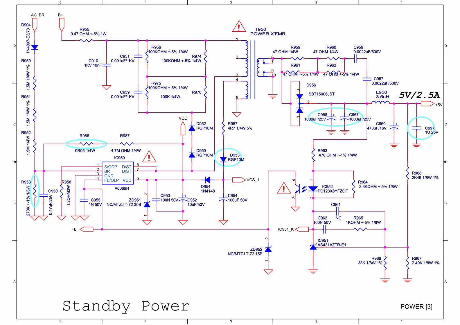
5
5
4
4
3
3
2
2
1
1
D D
C C
B B
A A
VCC
FB
+5V
AC_BR B+
VCS_1
IC951_K
!
!
!
5V/2.5A
Standby Power
D950RGP10MD950RGP10M
R974 100KOHM +-5% 1/4W
R974 100KOHM +-5% 1/4W
R963 470 OHM +-1% 1/4WR963 470 OHM +-1% 1/4W
C953100N 50VC953100N 50V
+C9581000uF/25V
+C9581000uF/25V
C9551N 50V
C9551N 50V
+ C9671000uF/25V
+ C9671000uF/25V
R975 100KOHM +-5% 1/4W
R975 100KOHM +-5% 1/4W
R9672.49K 1/8W 1%R9672.49K 1/8W 1%
IC951AS431AZTR-E1IC951AS431AZTR-E1
R986
0R05 1/4W
R986
0R05 1/4W
+ C954100uF 50V
+ C954100uF 50V
R951
1.5
M 1
/4W
1%
R951
1.5
M 1
/4W
1%
R9550.47 OHM +-5% 1W
R9550.47 OHM +-5% 1W
C962100N 50V
C962100N 50V
R96047 OHM 1/4W
R96047 OHM 1/4W
R976100K 1/4W
R976100K 1/4W
C9101KV 10nF
C9101KV 10nF
R9682K49 1/8W 1%R9682K49 1/8W 1%
D9541N4148D9541N4148
C9971U 25VC9971U 25V
ZD951NC/MTZJ T-72 30B
ZD951NC/MTZJ T-72 30B
12
R952
1.5
M 1
/4W
R952
1.5
M 1
/4W
IC952PC123X8YFZOF
IC952PC123X8YFZOF
12
43
D9041N
4007-E
3/7
3D904
1N
4007-E
3/7
3
D953RGP10M
D953RGP10M
D952RGP10MD952RGP10M
C9560.0022uF/500VC9560.0022uF/500V
C9590.001uF/1KV
C9590.001uF/1KV
R956 100KOHM +-5% 1/4W
R956 100KOHM +-5% 1/4W
R961
47 OHM +-5% 1/4W
R961
47 OHM +-5% 1/4W
IC950
A6069H
IC950
A6069H
S/OCP1
BR2
GND3
FB/OLP4
VCC5
D/ST7
D/ST8
T950POWER X'FMR
T950POWER X'FMR
1
2
3
5
4
76
910
R95947 OHM 1/4W
R95947 OHM 1/4W
+
C95210uF/50V
+
C95210uF/50V
R953
270K
+-1
% 1
/8W
R953
270K
+-1
% 1
/8W
C9570.0022uF/500V
C9570.0022uF/500V
R965 1KOHM +-5% 1/8W
R965 1KOHM +-5% 1/8W
L9503.5uHL9503.5uH
R958
1.2
OH
M2W
R958
1.2
OH
M2W
ZD952NC/MTZJ T-72 15B
ZD952NC/MTZJ T-72 15B
12
C950
0.4
7uF
/25V
C950
0.4
7uF
/25V
R987
4.7M OHM 1/4W
R987
4.7M OHM 1/4W
R962
47 OHM +-5% 1/4W
R962
47 OHM +-5% 1/4W
R96633K 1/8W 1%
R96633K 1/8W 1%
C9510.001uF/1KV
C9510.001uF/1KVR950
1.5
M 1
/4W
1%
R950
1.5
M 1
/4W
1%
C961
NC
C961
NC
R9574R7 1/4W 5%R9574R7 1/4W 5%
D956
SBT15006JST
D956
SBT15006JST
1
2
3
R964 3.3KOHM +-5% 1/8WR964 3.3KOHM +-5% 1/8W
+C960470uF/16V
+C960470uF/16V
POWER [3]
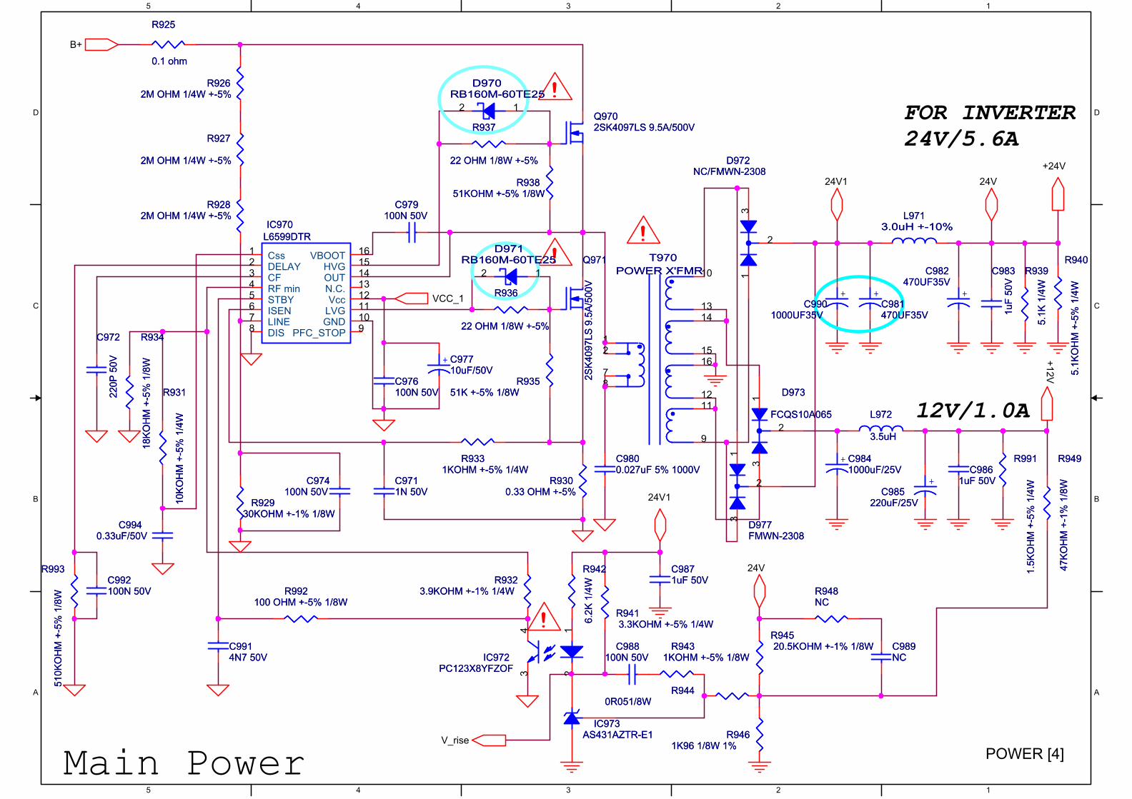
5
5
4
4
3
3
2
2
1
1
D D
C C
B B
A A
24V
VCC_1
+24V
24V1 24V
+12V
B+
24V1
V_rise
!
!
!
!
12V/1.0A
FOR INVERTER
24V/5.6A
Main Power
R9440R051/8W
R9440R051/8W
R940
5.1
KO
HM
+-5
% 1
/4W
R940
5.1
KO
HM
+-5
% 1
/4W
C9940.33uF/50V
C9940.33uF/50V
R993
510K
OH
M +
-5%
1/8
W
R993
510K
OH
M +
-5%
1/8
W
Q9702SK4097LS 9.5A/500VQ9702SK4097LS 9.5A/500V
R941 3.3KOHM +-5% 1/4WR941 3.3KOHM +-5% 1/4W
R9461K96 1/8W 1%
R9461K96 1/8W 1%
D970RB160M-60TE25
D970RB160M-60TE25
12
R939
5.1
K 1
/4W
R939
5.1
K 1
/4W
C9711N 50VC9711N 50V
R934
18K
OH
M +
-5%
1/8
W
R934
18K
OH
M +
-5%
1/8
W
R938 51KOHM +-5% 1/8W
R938 51KOHM +-5% 1/8W
C9914N7 50VC9914N7 50V
+
C982470UF35V
+
C982470UF35V
C989NCC989NC
+ C97710uF/50V
+ C97710uF/50V
R93551K +-5% 1/8W
R93551K +-5% 1/8W
R992 100 OHM +-5% 1/8W
R992 100 OHM +-5% 1/8W
R932 3.9KOHM +-1% 1/4W
R932 3.9KOHM +-1% 1/4W
+
C985220uF/25V
+
C985220uF/25V
C992100N 50VC992100N 50V
C9871uF 50VC9871uF 50V
R991
1.5
KO
HM
+-5
% 1
/4W
R991
1.5
KO
HM
+-5
% 1
/4W
R943 1KOHM +-5% 1/8W
R943 1KOHM +-5% 1/8W
R949
47K
OH
M +
-1%
1/8
W
R949
47K
OH
M +
-1%
1/8
W
D973
FCQS10A065
D973
FCQS10A065
1
2
3
R936
22 OHM 1/8W +-5%
R936
22 OHM 1/8W +-5%
C9800.027uF 5% 1000VC9800.027uF 5% 1000V
Q971
2S
K4097LS
9.5
A/5
00V
Q971
2S
K4097LS
9.5
A/5
00V
C976100N 50VC976100N 50VR931
10K
OH
M +
-5%
1/4
W
R931
10K
OH
M +
-5%
1/4
W
T970
POWER X'FMR
T970
POWER X'FMR
12
78
1413
10
15
1211
9
16
R925
0.1 ohm
R925
0.1 ohm
R933 1KOHM +-5% 1/4W
R933 1KOHM +-5% 1/4W
R9282M OHM 1/4W +-5%
R9282M OHM 1/4W +-5%
R948NCR948NC
C972
220P
50V
C972
220P
50V
C974100N 50V
C974100N 50V
C988100N 50V
C988100N 50V
R9300.33 OHM +-5%
R9300.33 OHM +-5%
R942
6.2
K 1
/4W
R942
6.2
K 1
/4W
D972NC/FMWN-2308
D972NC/FMWN-2308
1
2
3
IC972PC123X8YFZOF
IC972PC123X8YFZOF
12
43
R927
2M OHM 1/4W +-5%
R927
2M OHM 1/4W +-5%
+
C981470UF35V
+
C981470UF35V
+ C9841000uF/25V
+ C9841000uF/25V
R945 20.5KOHM +-1% 1/8WR945 20.5KOHM +-1% 1/8W
D977FMWN-2308D977FMWN-2308
1
2
3IC973
AS431AZTR-E1IC973
AS431AZTR-E1
R929 30KOHM +-1% 1/8W
R929 30KOHM +-1% 1/8W
C9861uF 50V
C9861uF 50V
R9262M OHM 1/4W +-5%
R9262M OHM 1/4W +-5%
C983
1uF
50V
C983
1uF
50V
C979100N 50V
C979100N 50V
+
C9901000UF35V
+
C9901000UF35V
R937
22 OHM 1/8W +-5%
R937
22 OHM 1/8W +-5%
L972
3.5uH
L972
3.5uH
D971RB160M-60TE25
D971RB160M-60TE25
12
L9713.0uH +-10%
L9713.0uH +-10%IC970
L6599DTR
IC970
L6599DTR
Css1
DELAY2
CF3
RF min4
STBY5
ISEN6
LINE7
DIS8
VBOOT16
HVG15
PFC_STOP9
GND10
LVG11
Vcc12
N.C.13
OUT14
POWER [4]
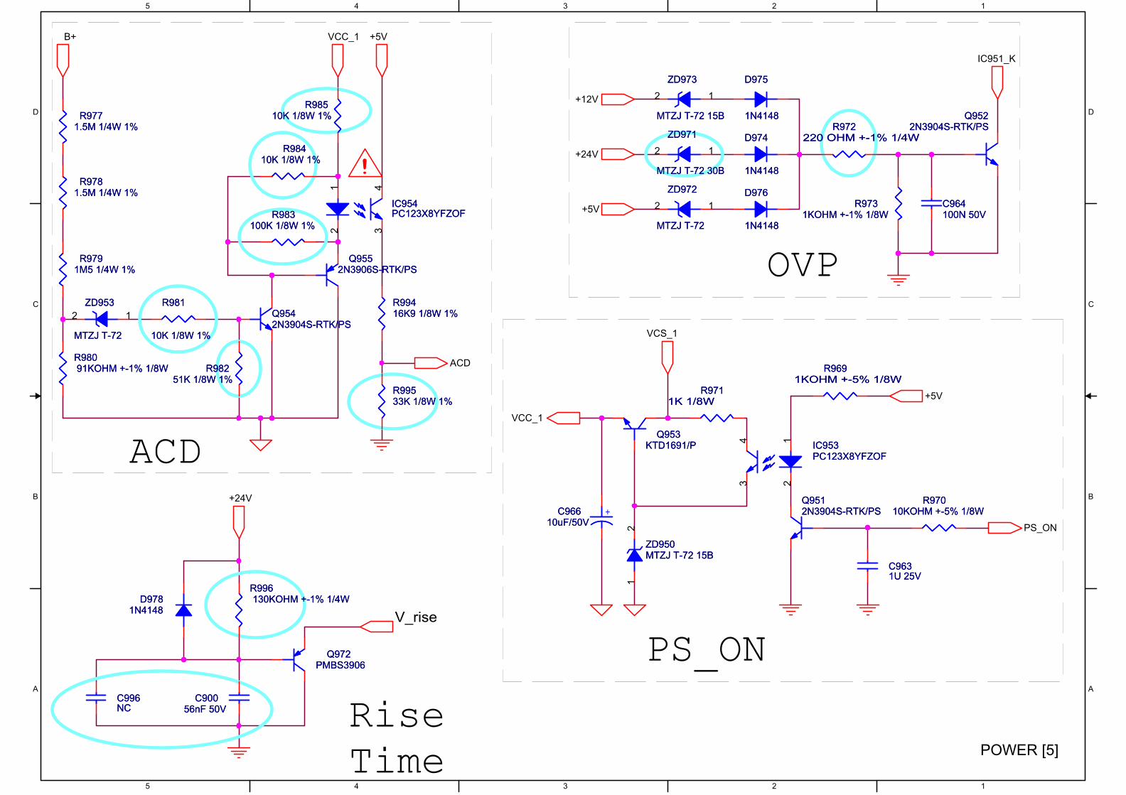
5
5
4
4
3
3
2
2
1
1
D D
C C
B B
A A
+5V
ACD
B+ VCC_1
+5V
+24V
+12V
IC951_K
VCS_1
+5V
VCC_1
PS_ON
V_rise
+24V
!
ACD
OVP
PS_ON
RiseTime
D9781N4148
D9781N4148
R99533K 1/8W 1%R99533K 1/8W 1%
R9791M5 1/4W 1%
R9791M5 1/4W 1%
D974
1N4148
D974
1N4148
R9711K 1/8W
R9711K 1/8W
C9631U 25VC9631U 25V
D976
1N4148
D976
1N4148
Q972PMBS3906
Q972PMBS3906
ZD971
MTZJ T-72 30B
ZD971
MTZJ T-72 30B
12
R98510K 1/8W 1%
R98510K 1/8W 1%
Q9552N3906S-RTK/PS
Q9552N3906S-RTK/PS
C964100N 50VC964100N 50V
ZD953
MTZJ T-72
ZD953
MTZJ T-72
12
R9781.5M 1/4W 1%
R9781.5M 1/4W 1%
IC953PC123X8YFZOFIC953PC123X8YFZOF
12
43
ZD973
MTZJ T-72 15B
ZD973
MTZJ T-72 15B
12
R980 91KOHM +-1% 1/8WR980 91KOHM +-1% 1/8W
R9771.5M 1/4W 1%
R9771.5M 1/4W 1%
R996 130KOHM +-1% 1/4WR996 130KOHM +-1% 1/4W
D975
1N4148
D975
1N4148
C996NCC996NC
R969 1KOHM +-5% 1/8W
R969 1KOHM +-5% 1/8W
R981
10K 1/8W 1%
R981
10K 1/8W 1%
R99416K9 1/8W 1%R99416K9 1/8W 1%
ZD972
MTZJ T-72
ZD972
MTZJ T-72
12
R98251K 1/8W 1%
R98251K 1/8W 1%
Q9522N3904S-RTK/PS
Q9522N3904S-RTK/PS
C90056nF 50V
C90056nF 50V
R970 10KOHM +-5% 1/8W
R970 10KOHM +-5% 1/8W
R972 220 OHM +-1% 1/4W
R972 220 OHM +-1% 1/4W
Q953KTD1691/P
Q953KTD1691/P
R973 1KOHM +-1% 1/8W
R973 1KOHM +-1% 1/8W
R98410K 1/8W 1%
R98410K 1/8W 1%
+C96610uF/50V
+C96610uF/50V
Q9542N3904S-RTK/PSQ9542N3904S-RTK/PS
Q9512N3904S-RTK/PSQ9512N3904S-RTK/PS
IC954PC123X8YFZOFIC954PC123X8YFZOF
12
43
ZD950MTZJ T-72 15BZD950MTZJ T-72 15B
12
R983100K 1/8W 1%
R983100K 1/8W 1%
POWER [5]
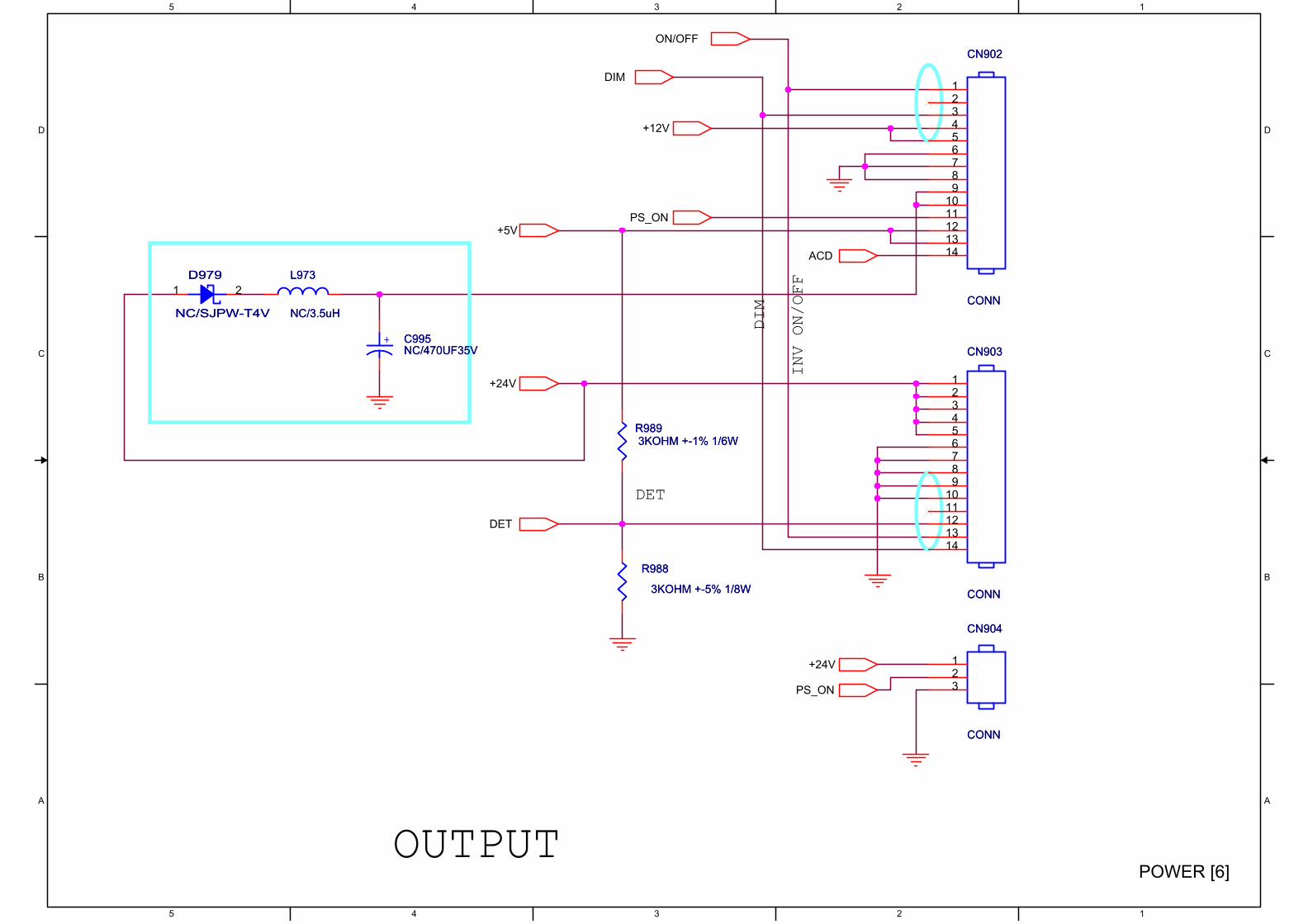
5
5
4
4
3
3
2
2
1
1
D D
C C
B B
A A
PS_ON
ON/OFF
DIM
+5V
ACD
DET
+24V
+12V
+24V
PS_ON
INV ON/OFF
DIM
DET
OUTPUT
CN902
CONN
CN902
CONN
123456789
1011121314
CN904
CONN
CN904
CONN
123
R988
3KOHM +-5% 1/8W
R988
3KOHM +-5% 1/8W
L973
NC/3.5uH
L973
NC/3.5uH
+ C995NC/470UF35V
+ C995NC/470UF35V CN903
CONN
CN903
CONN
123456789
1011121314
D979
NC/SJPW-T4V
D979
NC/SJPW-T4V
1 2
R989 3KOHM +-1% 1/6WR989 3KOHM +-1% 1/6W
POWER [6]
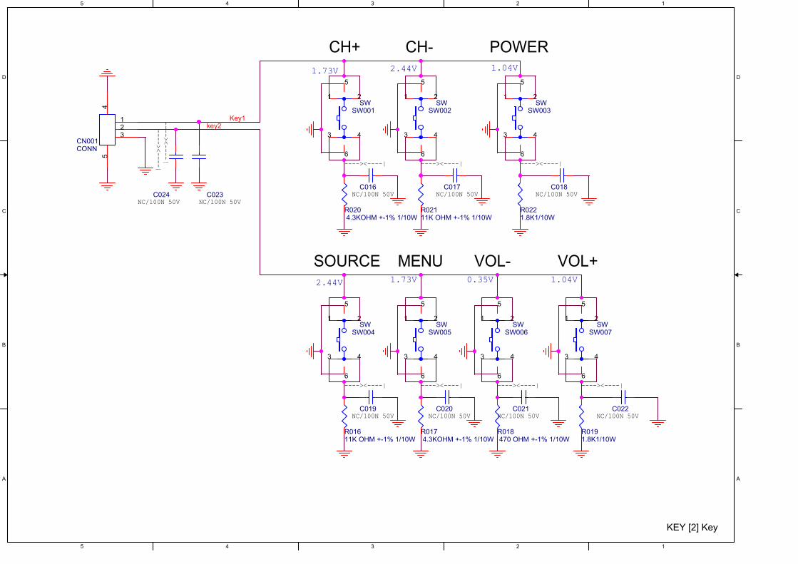
5
5
4
4
3
3
2
2
1
1
D D
C C
B B
A A
NC/100N 50V
NC/100N 50V
NC/100N 50V
POWERCH-CH+
2.44V
----><----|----><----|
----><----|
NC/100N 50V
----><----|
NC/100N 50V
VOL-1.73V
NC/100N 50V
----><----|
VOL+
2.44V
1.04V
SOURCE
----><----|
1.73V
0.35V
NC/100N 50V
NC/100N 50V
----><----|
MENU
NC/100N 50V
----><----|
1.04V
----><----|
Key1key2
SW004SW
3 4
21
5
6
SW005SW
3 4
21
5
6
C021
R0191.8K1/10W
C016
R018 470 OHM +-1% 1/10W
C019
R02111K OHM +-1% 1/10W
SW001SW
3 4
21
5
6
SW007SW
3 4
21
5
6
SW003SW
3 4
21
5
6
C022
R020 4.3KOHM +-1% 1/10W
R0221.8K1/10W
C017
C020
SW002SW
3 4
21
5
6
SW006SW
3 4
21
5
6
CN001CONN
123
45
C023C024
R017 4.3KOHM +-1% 1/10W
C018
R01611K OHM +-1% 1/10W
KEY [2] Key
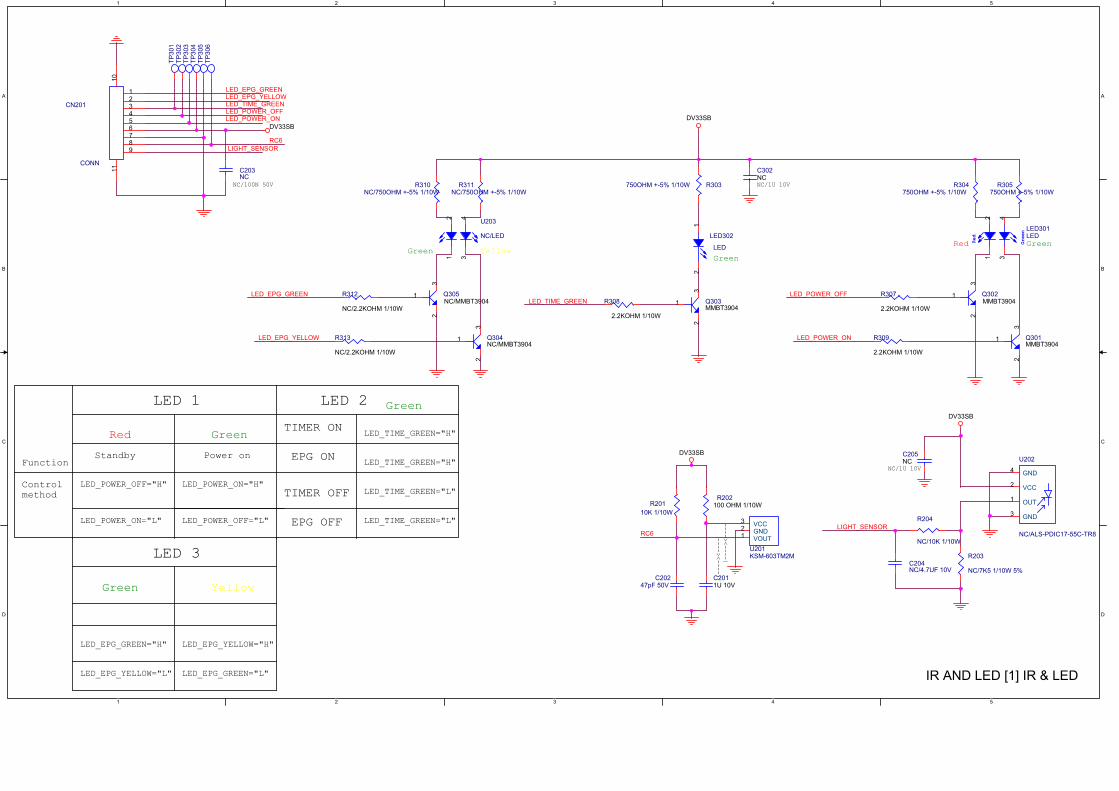
1
1
2
2
3
3
4
4
5
5
A A
B B
C C
D D
Green
----><----|
NC/1U 10V
Red Green
----><----|
NC/1U 10V
YellowGreen
NC/100N 50V
LED 2
LED_POWER_OFF="L"
EPG ON
TIMER ON
EPG OFF
TIMER OFF
LED 1
Function
Controlmethod
Standby
LED_TIME_GREEN="H"
LED_POWER_ON="L"
Power on
Green
LED_POWER_ON="H"LED_POWER_OFF="H"
GreenRed
Green
LED 3
Yellow
LED_EPG_GREEN="H"
LED_TIME_GREEN="H"
LED_TIME_GREEN="L"
LED_TIME_GREEN="L"
LED_EPG_GREEN="L"
LED_EPG_YELLOW="H"
LED_EPG_YELLOW="L"
LED_POWER_ON
LED_TIME_GREENLED_POWER_OFF
RC6LIGHT_SENSOR
LED_EPG_YELLOW
LED_EPG_GREEN
LED_POWER_OFFLED_POWER_ON
LED_EPG_YELLOW
LIGHT_SENSOR
LED_EPG_GREEN
RC6
LED_TIME_GREEN
DV33SB
DV33SB
DV33SB
DV33SB
TP
303
R313
NC/2.2KOHM 1/10W
Green
Red
LED301LED
12
34
R311NC/750OHM +-5% 1/10W
TP
305
R303750OHM +-5% 1/10W
CN201
CONN
123456789
10
11
Q301MMBT3904
3
1
2
Q305NC/MMBT3904
3
1
2
C20247pF 50V
C203NC
R204
NC/10K 1/10WU201KSM-603TM2M
123
VOUTGNDVCC
R312
NC/2.2KOHM 1/10W
TP
304
R309
2.2KOHM 1/10W
TP
306
R202100 OHM 1/10W
R307
2.2KOHM 1/10W
R304750OHM +-5% 1/10W
R201
10K 1/10W
C302NC
R310NC/750OHM +-5% 1/10W
U203
NC/LED
2 4
1 3
R305750OHM +-5% 1/10W
Q302MMBT3904
3
1
2
LED302
LED
12
C205NC
TP
301
U202
NC/ALS-PDIC17-55C-TR8
3
1
2
4
GND
OUT
VCC
GND
R203
NC/7K5 1/10W 5%
Q303MMBT3904
3
1
2
TP
302
Q304NC/MMBT3904
3
1
2
R308
2.2KOHM 1/10W
C204NC/4.7UF 10V
C2011U 10V
IR AND LED [1] IR & LED
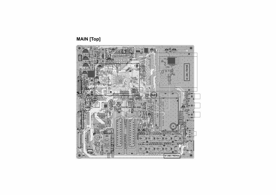
MAIN [Top]
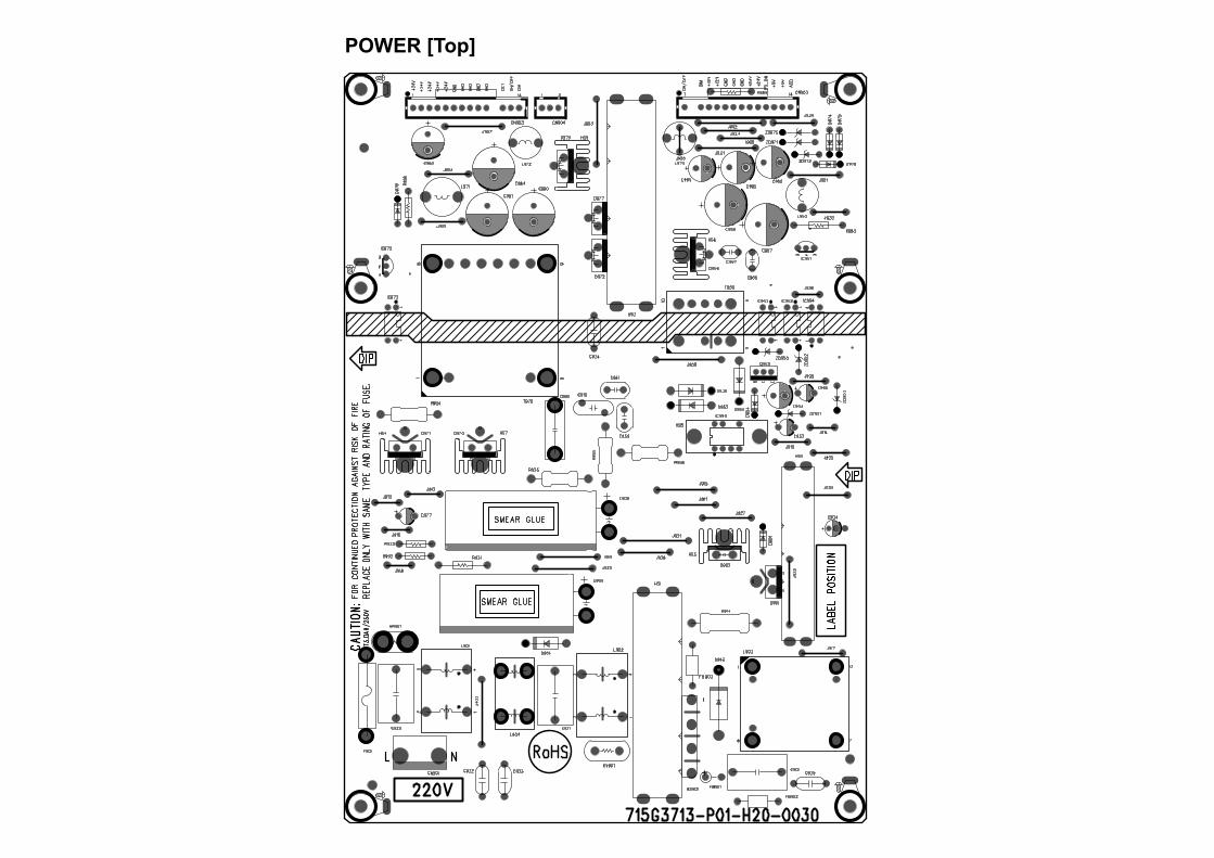
POWER [Top]
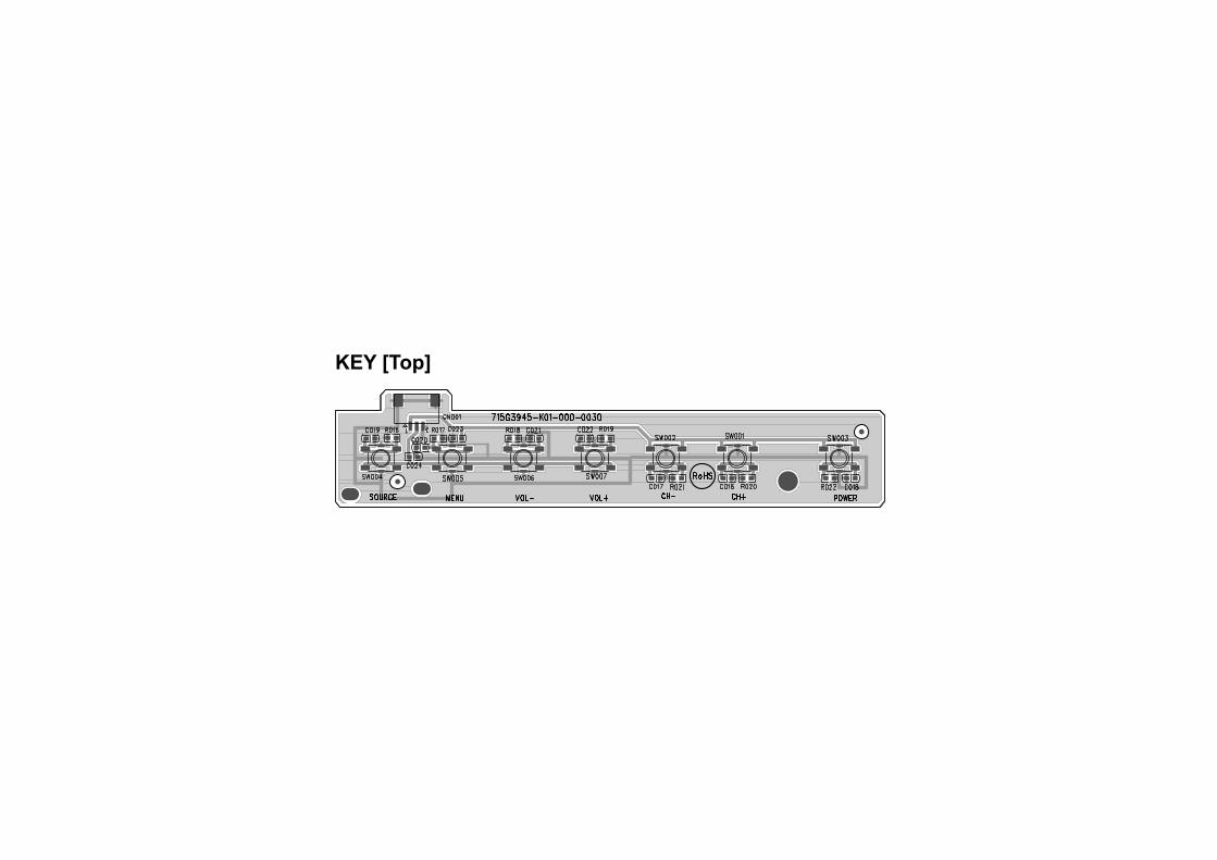
KEY [Top]
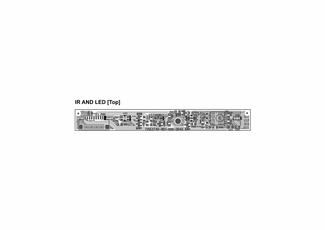
IR AND LED [Top]
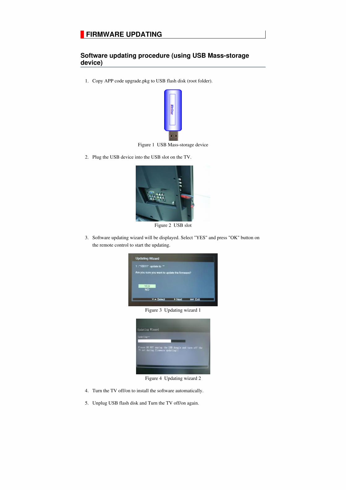
FIRMWARE UPDATING
Software updating procedure (using USB Mass-storage device)
1. Copy APP code upgrade.pkg to USB flash disk (root folder).
Figure 1 USB Mass-storage device
2. Plug the USB device into the USB slot on the TV.
Figure 2 USB slot
3. Software updating wizard will be displayed. Select "YES" and press "OK" button on
the remote control to start the updating.
Figure 3 Updating wizard 1
Figure 4 Updating wizard 2
4. Turn the TV off/on to install the software automatically.
5. Unplug USB flash disk and Turn the TV off/on again.
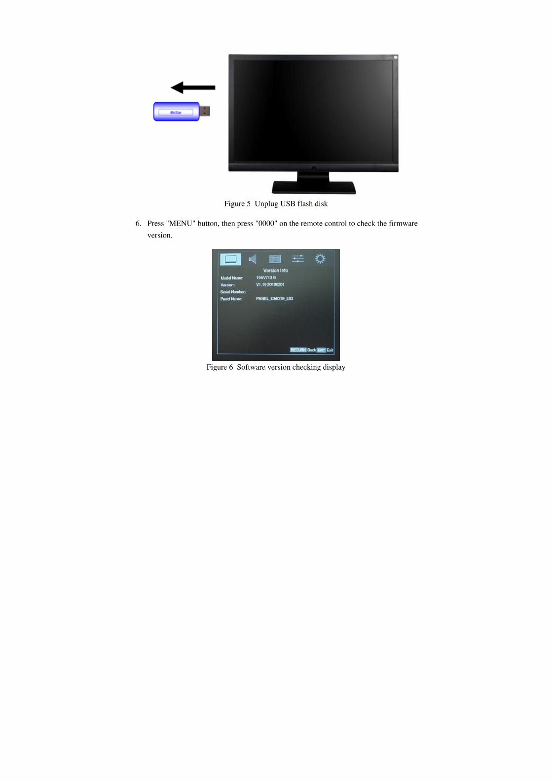
Figure 5 Unplug USB flash disk
6. Press "MENU" button, then press "0000" on the remote control to check the firmware
version.
Figure 6 Software version checking display

TECHNICAL BULLETIN
File Name Title issuing date

PARTS LIST
Precaution
Note:
The part number must be used when ordering parts, in order to assist in processing, be
sure to include the Model number and Description.
The PC board assembly with mark is no longer available after the end of the
production.
Abbreviations
All CD and PF capacitors are ±5 %, 50 V and all resistor, ±5 %, 1/6 W unless otherwise
noted.
WARNING: BEFORE SERVICING THIS CHASSIS, READ THE "SAFETY
PRECAUTION" AND "PRODUCT SAFETY NOTICE".
CAUTION: The international hazard symbols " " in the schematic diagram
and the parts list designate components which have special characteristics
important for safety and should be replaced only with types identical to
those in the original circuit or specified in the parts list.
The mounting position of replacements is to be identical with originals.
Before replacing any of these components, read carefully the "SAFETY
PRECAUTION" and "PRODUCT SAFETY NOTICE".
Do not degrade the safety of the receiver through improper servicing.
Capacitors CD : Ceramic Disk
Resistors CF : Carbon film
OMF : Oxide Metal Film
PF : Plastic Film
CC : Carbon Composition
VR : Variable Resistor
EL : Electrolytic
MF : Metal Film
FR : Fusible Resistor

PARTS LIST
Block : 6↓Select
Location : Search Page :
1 / 1 JumpJump
Parts No. : Search
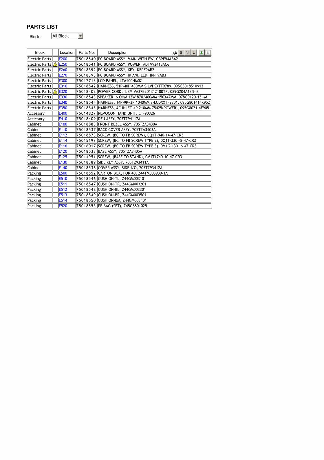
PARTS LIST
Block : 6All Block
Block Location Parts No. Description S MM L
Electric Parts E200 75018540 PC BOARD ASSY, MAIN WITH FW, CBPF94ABA2
Electric Parts E250 75018541 PC BOARD ASSY, POWER, ADTV92418AC6
Electric Parts E260 75018392 PC BOARD ASSY, KEY, KEPF9AB2
Electric Parts E270 75018393 PC BOARD ASSY, IR AND LED, IRPF9AB3
Electric Parts E300 75017713 LCD PANEL, LTA400HM02
Electric Parts E310 75018542 HARNESS, 51P-40P 430MM S-LVDSXTF9789, 095G801851X913
Electric Parts E320 75018402 POWER CORD, 1.8M VA37B201312180TP, 089G204A18N-IS
Electric Parts E330 75018543 SPEAKER, 6 OHM 12W 870/460MM 150X47MM, 078G0120-13--M
Electric Parts E340 75018544 HARNESS, 14P-9P+3P 1040MM S-LCDXXTF9801, 095G801414X952
Electric Parts E350 75018545 HARNESS, AC INLET-4P 210MM 75425(POWER), 095G8021-4F905
Accessory E400 75014827 REMOCON HAND UNIT, CT-90326
Accessory E410 75018409 DFU ASSY, 705TZ94117A
Cabinet E100 75018883 FRONT BEZEL ASSY, 705TZA3430A
Cabinet E110 75018537 BACK COVER ASSY, 705TZA3403A
Cabinet E112 75018873 SCREW, (BC TO FB SCREW), 0Q1T-940-14-47-CR3
Cabinet E114 75015193 SCREW, (BC TO FB SCREW TYPE 2), 0Q1T-330--8-47-CR3
Cabinet E116 75016017 SCREW, (BC TO FB SCREW TYPE 3), 0M1G-130--6-47-CR3
Cabinet E120 75018538 BASE ASSY, 705TZA3405A
Cabinet E125 75014951 SCREW, (BASE TO STAND), 0M1T1740-10-47-CR3
Cabinet E130 75018389 SIDE KEY ASSY, 705TZ93411A
Cabinet E140 75018536 COVER ASSY, SIDE-I/O, 705TZ93412A
Packing E500 75018552 CARTON BOX, FOR 40, Z44TM003939-1A
Packing E510 75018546 CUSHION-TL, Z44GM003101
Packing E511 75018547 CUSHION-TR, Z44GM003201
Packing E512 75018548 CUSHION-BL, Z44GM003301
Packing E513 75018549 CUSHION-BR, Z44GM003501
Packing E514 75018550 CUSHION-BM, Z44GM003401
Packing E520 75018553 PE BAG (SET), Z45G8801025
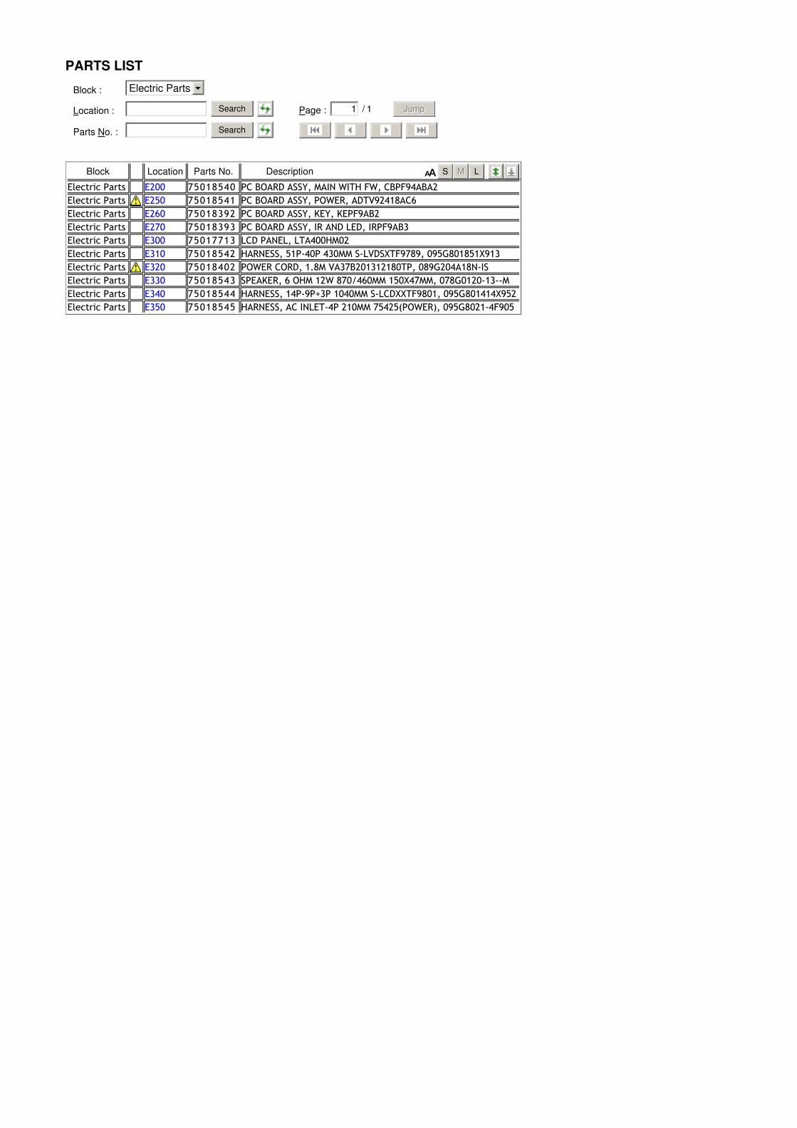
PARTS LIST
Block : 6Electric Parts
Location : Search Page :
1 / 1 JumpJump
Parts No. : Search
Block Location Parts No. Description S MM L
Electric Parts E200 75018540 PC BOARD ASSY, MAIN WITH FW, CBPF94ABA2
Electric Parts E250 75018541 PC BOARD ASSY, POWER, ADTV92418AC6
Electric Parts E260 75018392 PC BOARD ASSY, KEY, KEPF9AB2
Electric Parts E270 75018393 PC BOARD ASSY, IR AND LED, IRPF9AB3
Electric Parts E300 75017713 LCD PANEL, LTA400HM02
Electric Parts E310 75018542 HARNESS, 51P-40P 430MM S-LVDSXTF9789, 095G801851X913
Electric Parts E320 75018402 POWER CORD, 1.8M VA37B201312180TP, 089G204A18N-IS
Electric Parts E330 75018543 SPEAKER, 6 OHM 12W 870/460MM 150X47MM, 078G0120-13--M
Electric Parts E340 75018544 HARNESS, 14P-9P+3P 1040MM S-LCDXXTF9801, 095G801414X952
Electric Parts E350 75018545 HARNESS, AC INLET-4P 210MM 75425(POWER), 095G8021-4F905
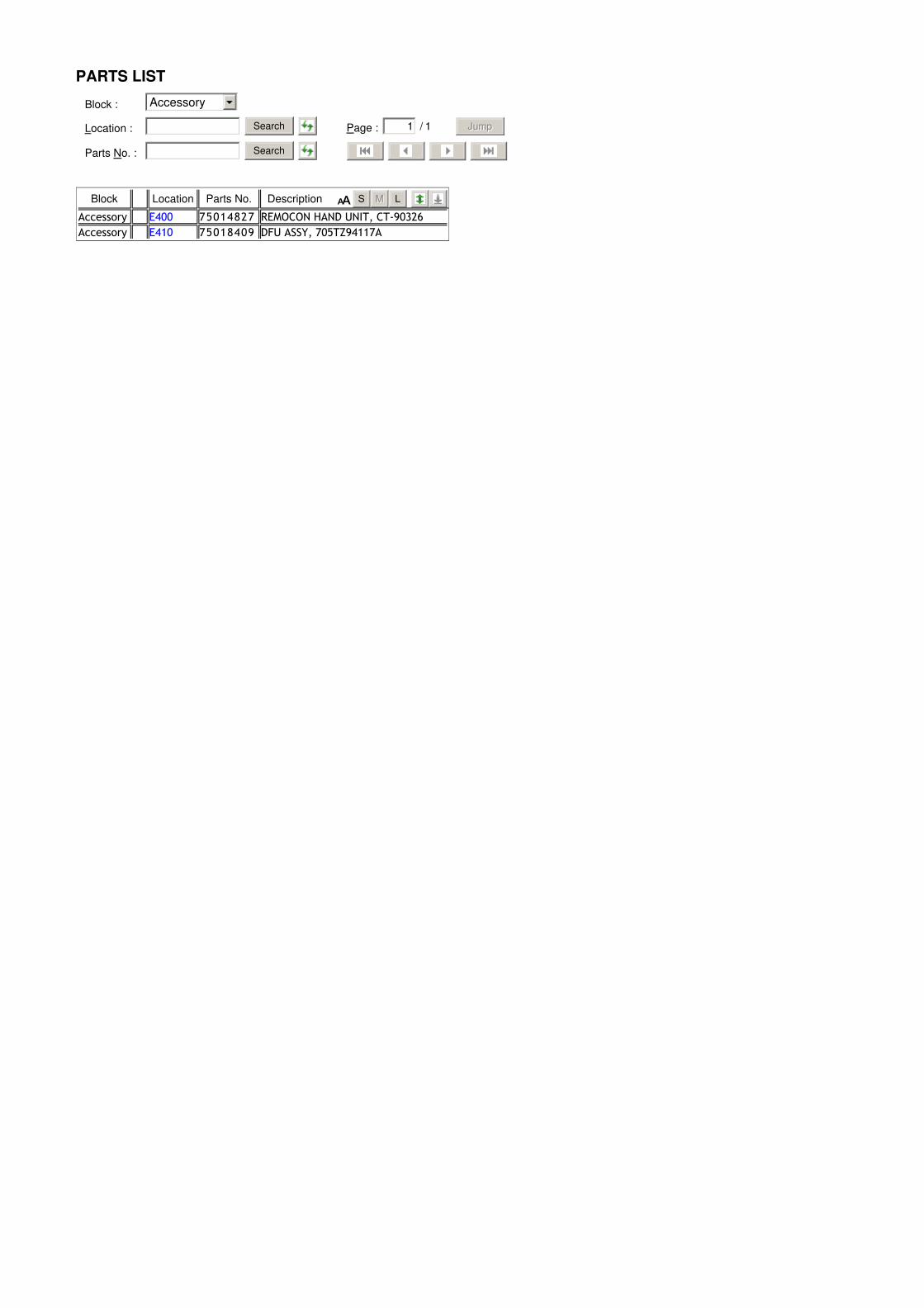
PARTS LIST
Block : 6Accessory
Location : Search Page :
1 / 1 JumpJump
Parts No. : Search
Block Location Parts No. Description S MM L
Accessory E400 75014827 REMOCON HAND UNIT, CT-90326
Accessory E410 75018409 DFU ASSY, 705TZ94117A
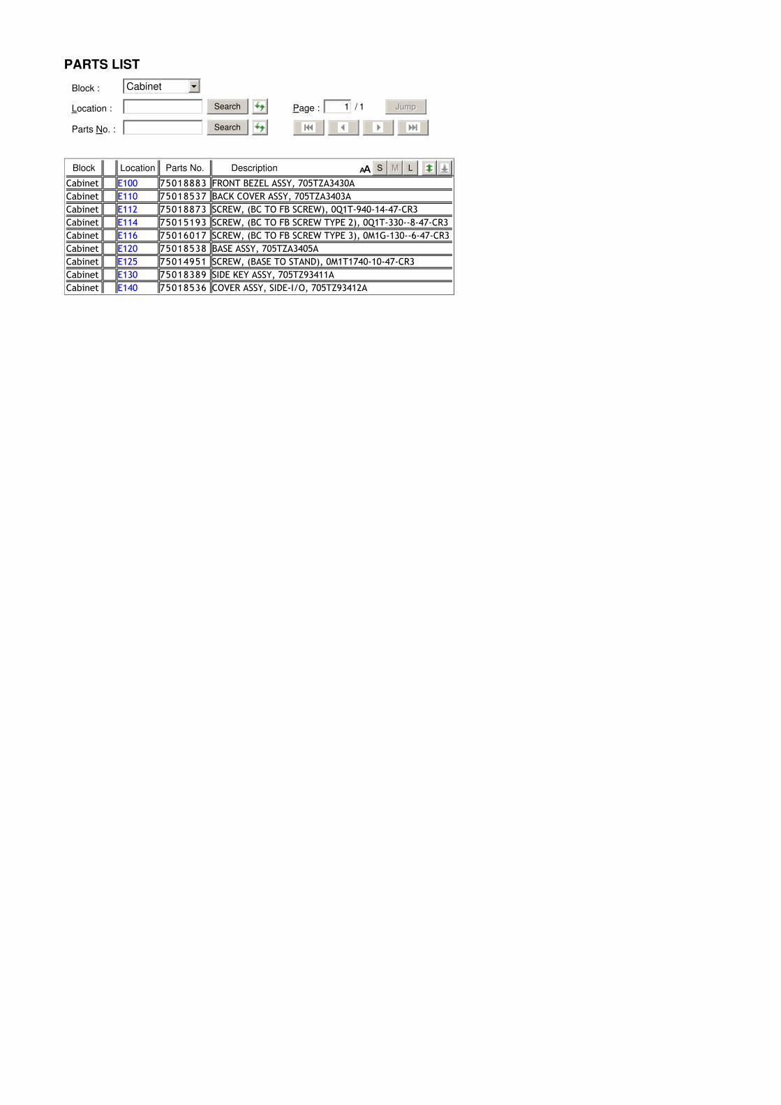
PARTS LIST
Block : 6Cabinet
Location : Search Page :
1 / 1 JumpJump
Parts No. : Search
Block Location Parts No. Description S MM L
Cabinet E100 75018883 FRONT BEZEL ASSY, 705TZA3430A
Cabinet E110 75018537 BACK COVER ASSY, 705TZA3403A
Cabinet E112 75018873 SCREW, (BC TO FB SCREW), 0Q1T-940-14-47-CR3
Cabinet E114 75015193 SCREW, (BC TO FB SCREW TYPE 2), 0Q1T-330--8-47-CR3
Cabinet E116 75016017 SCREW, (BC TO FB SCREW TYPE 3), 0M1G-130--6-47-CR3
Cabinet E120 75018538 BASE ASSY, 705TZA3405A
Cabinet E125 75014951 SCREW, (BASE TO STAND), 0M1T1740-10-47-CR3
Cabinet E130 75018389 SIDE KEY ASSY, 705TZ93411A
Cabinet E140 75018536 COVER ASSY, SIDE-I/O, 705TZ93412A
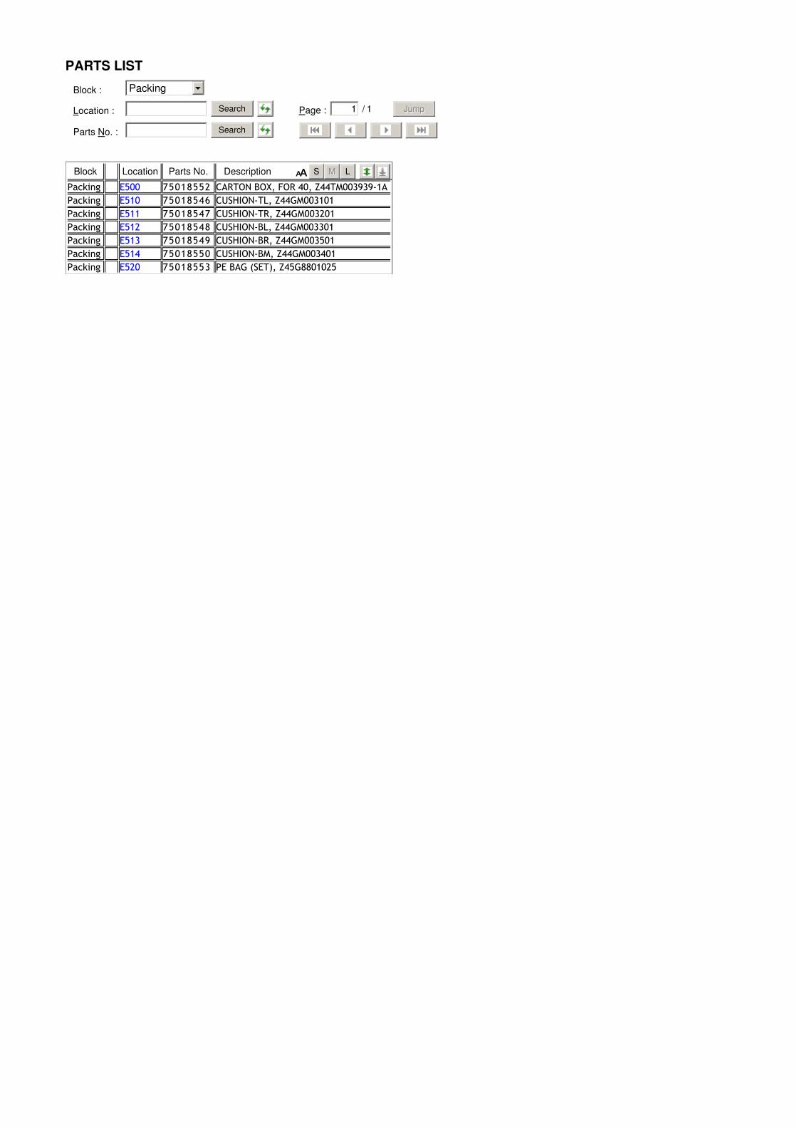
PARTS LIST
Block : 6Packing
Location : Search Page :
1 / 1 JumpJump
Parts No. : Search
Block Location Parts No. Description S MM L
Packing E500 75018552 CARTON BOX, FOR 40, Z44TM003939-1A
Packing E510 75018546 CUSHION-TL, Z44GM003101
Packing E511 75018547 CUSHION-TR, Z44GM003201
Packing E512 75018548 CUSHION-BL, Z44GM003301
Packing E513 75018549 CUSHION-BR, Z44GM003501
Packing E514 75018550 CUSHION-BM, Z44GM003401
Packing E520 75018553 PE BAG (SET), Z45G8801025
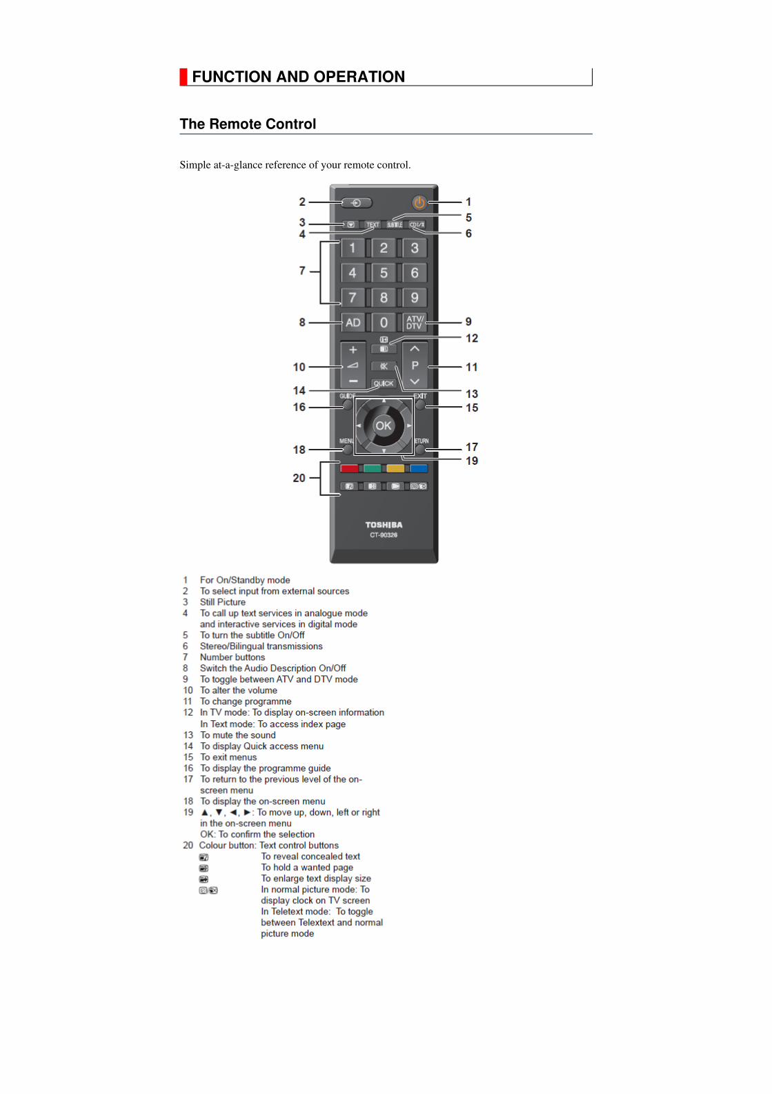
FUNCTION AND OPERATION
The Remote Control
Simple at-a-glance reference of your remote control.
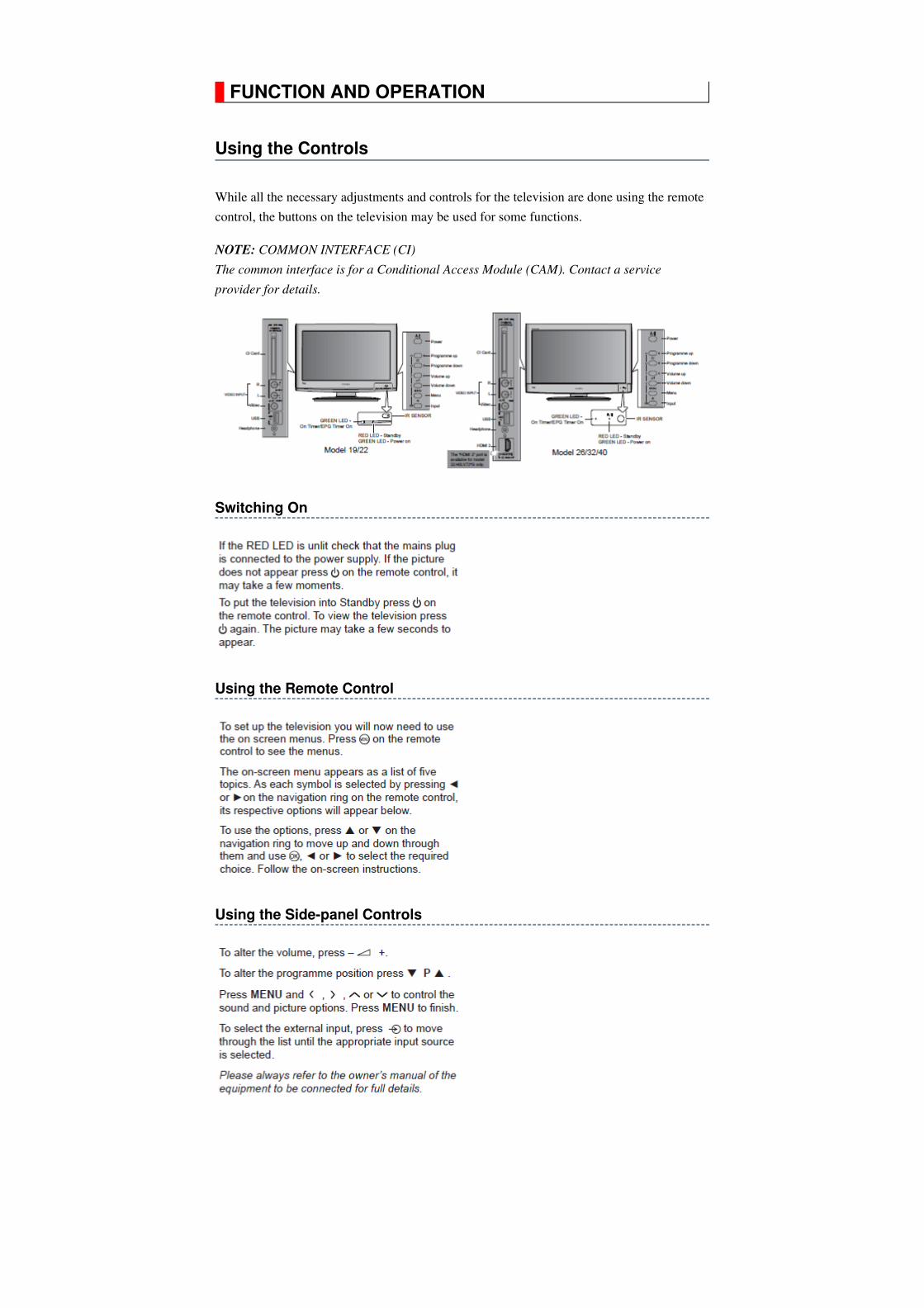
FUNCTION AND OPERATION
Using the Controls
While all the necessary adjustments and controls for the television are done using the remote
control, the buttons on the television may be used for some functions.
NOTE: COMMON INTERFACE (CI)
The common interface is for a Conditional Access Module (CAM). Contact a service
provider for details.
Switching On
Using the Remote Control
Using the Side-panel Controls
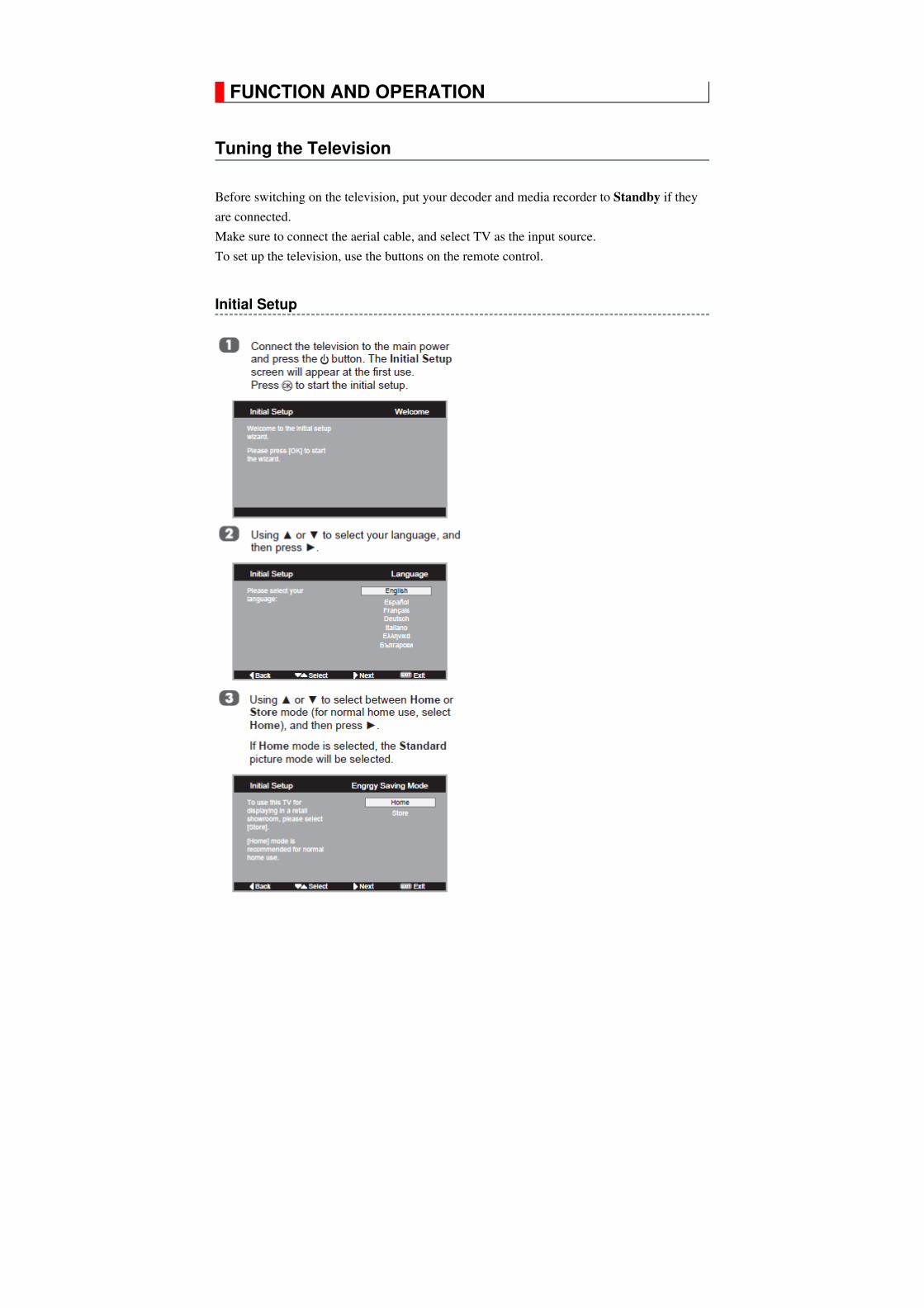
FUNCTION AND OPERATION
Tuning the Television
Before switching on the television, put your decoder and media recorder to Standby if they
are connected.
Make sure to connect the aerial cable, and select TV as the input source.
To set up the television, use the buttons on the remote control.
Initial Setup
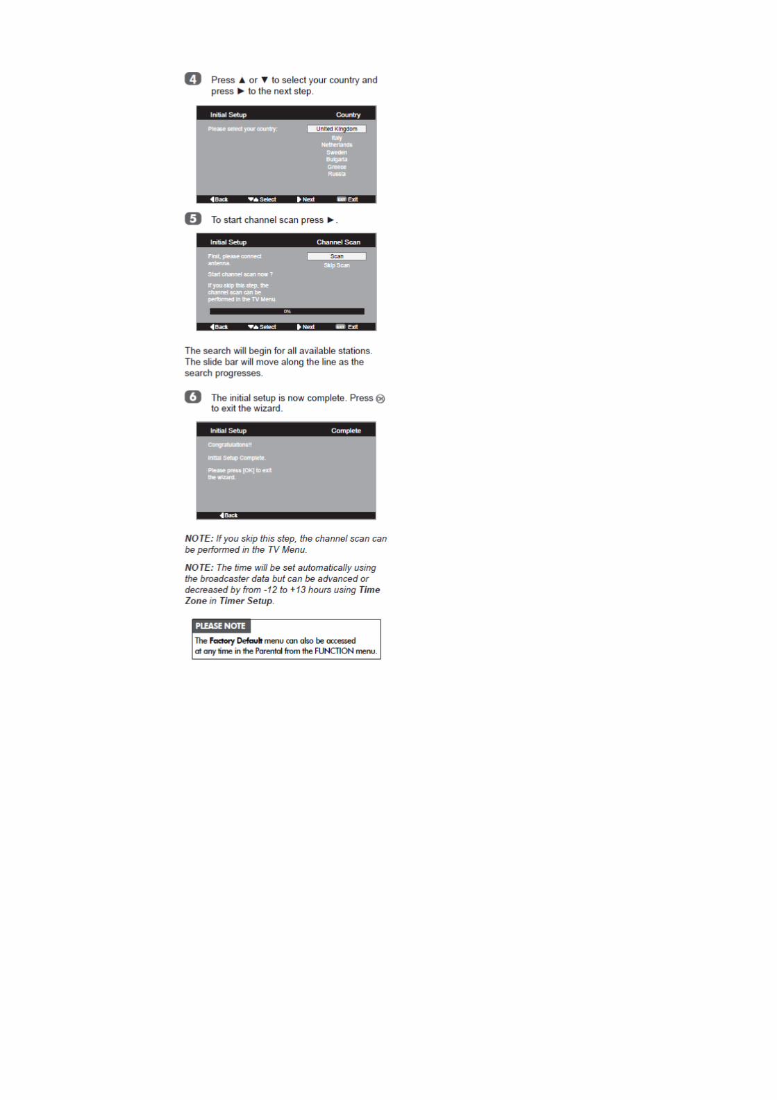
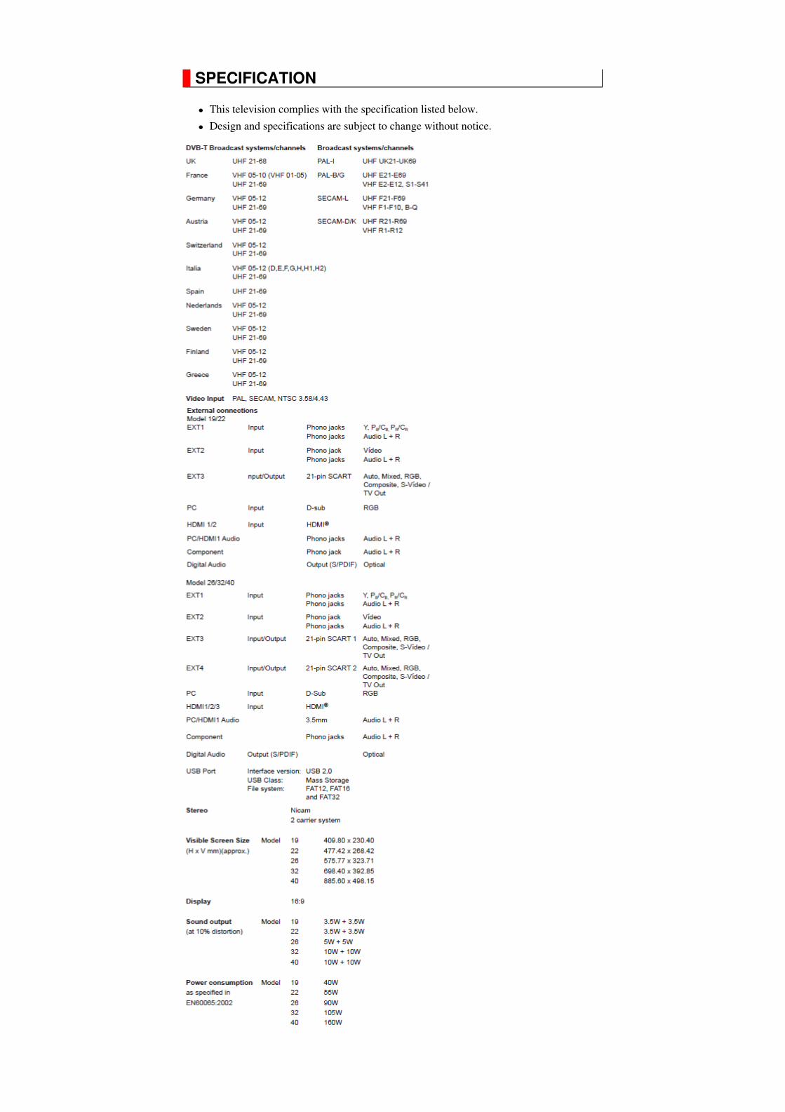
SPECIFICATION
This television complies with the specification listed below.
Design and specifications are subject to change without notice.