LC5500 Series Single-Stage Power Factor Corrected …LF 3054) TO-220F-7L (LF 3051) DIP8 •...
41
SANKEN ELECTRIC CO., LTD. Introduction The LC5500 series is the power IC for the LED driver which has an incorporated power MOSFET, designed for input capacitorless applications, and making it pos- sible for systems to comply with the harmonics standard (IEC61000-3-2 class C). The controller adapts the average current control method for realizing high power factors, and the quasi-resonant topology contributes to high efficiency and low EMI noise. The series is housed in either DIP8 or TO-220F-7L packages, depending on output power capability. The rich set of protection features helps to real- ize low component counts, and high performance-to-cost power supply. Features and Benefits • Non-isolated (LC551xD) and isolated (LC552xD and LC552xF) applications • Integrated on-time control circuit (it realizes high power factor by average current control) • Integrated startup circuit (no external startup circuit necessary) • Integrated soft-start circuit (reduces power stress during start-up on the incorporated power MOSFET and output rectifier) • Integrated bias assist circuit (improves startup performance, suppresses VCC voltage droop during operation, and allows use of low-rated ceramic capacitor on VCC pin) • Integrated Leading Edge Blanking (LEB) circuit • Integrated maximum on-time limit circuit LC5500 Series Single-Stage Power Factor Corrected Off-Line Switching Regulator ICs Figure 1. The LC5500 series packages for lower wattage versions are fully molded DIP8s, with pin 7 removed for greater isolation. For higher wattages, the TO-220F-7L fully molded package is provided, with three leadform options, all which provide a separation between pins 1 and 2. Application Information LC5500-AN, Rev. 1.7 TO-220F-7L (LF 3052) TO-220F-7L (LF 3054) TO-220F-7L (LF 3051) DIP8 • Protection features: ▫ Overcurrent protection (OCP): pulse-by-pulse ▫ Overvoltage protection (OVP): auto restart, OVP- activating pins vary by product series: OVP-Activating Pins Series VCC ISENSE OVP OCP LC551xD × × – × LC552xD × – × × LC552xF × – × × ▫ Overload protection (OLP): auto restart ▫ Thermal shutdown (TSD): latched shutdown The product lineup for the LC5500 series provides the following options: Part Number MOSFET V DSS (min) (V) R DS(on) (max) (Ω) Isolation Package P OUT * (W) 230 VAC 85 to 265 VAC LC5511D 650 3.95 Non- isolated DIP8 13 10 LC5513D 1.9 20 16 LC5521D 3.95 Isolated 13 10 LC5523D 1.9 20 16 LC5523F TO-220F- 7L 60 40 LC5525F 1.1 80 55 *Based on the thermal rating; the allowable maximum output power can be up to 120% to 140% of this value. However, maximum output power may be limited in an applications with low output voltage or short duty cycle. Part Number Assignment LC55nna A BCD A Product series name B Indicates non-isolated or isolated: 1 – Non-isolated, 2 – Isolated C On-resistance of the incorporated MOSFET: 1 – 3.95 Ω, 3 – 1.9 Ω, 5 – 1.1 Ω D Indicates the package: D – DIP8, F – TO-220F-7L Applications • LED lighting fixtures • LED light bulbs
Transcript of LC5500 Series Single-Stage Power Factor Corrected …LF 3054) TO-220F-7L (LF 3051) DIP8 •...

SANKEN ELECTRIC CO., LTD.
IntroductionThe LC5500 series is the power IC for the LED driver which has an incorporated power MOSFET, designed for input capacitorless applications, and making it pos-sible for systems to comply with the harmonics standard (IEC61000-3-2 class C). The controller adapts the average current control method for realizing high power factors, and the quasi-resonant topology contributes to high efficiency and low EMI noise. The series is housed in either DIP8 or TO-220F-7L packages, depending on output power capability. The rich set of protection features helps to real-ize low component counts, and high performance-to-cost power supply.
Features and Benefits• Non-isolated (LC551xD) and isolated (LC552xD and
LC552xF) applications• Integrated on-time control circuit (it realizes high power
factor by average current control)• Integrated startup circuit (no external startup circuit
necessary)• Integrated soft-start circuit (reduces power stress during
start-up on the incorporated power MOSFET and output rectifier)
• Integrated bias assist circuit (improves startup performance, suppresses VCC voltage droop during operation, and allows use of low-rated ceramic capacitor on VCC pin)
• Integrated Leading Edge Blanking (LEB) circuit• Integrated maximum on-time limit circuit
LC5500 Series Single-Stage Power Factor Corrected Off-Line Switching Regulator ICs
Figure 1. The LC5500 series packages for lower wattage versions are fully molded DIP8s, with pin 7 removed for greater isolation. For higher wattages, the TO-220F-7L fully molded package is provided, with three leadform options, all which provide a separation between pins 1 and 2.
Application Information
LC5500-AN, Rev. 1.7
TO-220F-7L (LF 3052)
TO-220F-7L (LF 3054)
TO-220F-7L (LF 3051)DIP8
• Protection features:▫ Overcurrent protection (OCP): pulse-by-pulse▫ Overvoltage protection (OVP): auto restart, OVP-
activating pins vary by product series:OVP-Activating Pins
Series VCC ISENSE OVP OCP
LC551xD × × – ×
LC552xD × – × ×
LC552xF × – × ×
▫ Overload protection (OLP): auto restart▫ Thermal shutdown (TSD): latched shutdown
The product lineup for the LC5500 series provides the following options:
Part Number
MOSFETVDSS(min)
(V)
RDS(on)(max)
(Ω)Isolation Package
POUT*(W)
230 VAC 85 to 265VAC
LC5511D
650
3.95 Non-isolated
DIP8
13 10
LC5513D 1.9 20 16
LC5521D 3.95
Isolated
13 10
LC5523D1.9
20 16
LC5523F TO-220F-7L
60 40
LC5525F 1.1 80 55
*Based on the thermal rating; the allowable maximum output power can be up to 120% to 140% of this value. However, maximum output power may be limited in an applications with low output voltage or short duty cycle.
Part Number Assignment
LC55nnaA BC D
A Product series name
B Indicates non-isolated or isolated: 1 – Non-isolated, 2 – Isolated
C On-resistance of the incorporated MOSFET: 1 – 3.95 Ω, 3 – 1.9 Ω, 5 – 1.1 Ω
D Indicates the package: D – DIP8, F – TO-220F-7L
Applications• LED lighting fixtures• LED light bulbs

2SANKEN ELECTRIC CO., LTD.
LC5500-AN, Rev. 1.7
Table of ContentsGeneral Specifications 1
Block Diagrams and Pin Descriptions 3Package Drawings 5Electrical Characteristics 9Application Circuit Examples 15
Functional Description 17On-Time Control Operation 17Startup Operation 19Operation Modes at Startup 22Soft-Start Function 22Quasi-Resonant Operation and Bottom-On Timing 23Latch Function 26Overvoltage Protection (OVP) 27Overload Protection (OLP) 31Overcurrent Protection (OCP) 33Input Compensation Function for Overcurrent Protection 34OCP Threshold Voltage with and without the OCP Input Compensation Circuit 34Thermal Shutdown Protection 36Maximum On-Time Limiting Function 36
Design Notes 36Peripheral Components 36Transformer Design 36Trace and Component Layout Design 38

3SANKEN ELECTRIC CO., LTD.
LC5500-AN, Rev. 1.7
S/GND
TSD
LEB
D/STSTARTUP
Reg
Bias
UVLO
VCC
OCP
OVP
OSC
OCP
DetectionBottom
Reg
ControlFeedback
OLP
⑧
①
②
③
④
Drv
COMP
⑥ ISENSE
QSR
OTA
⑤NF
Control Part
Figure 2. LC551xD series functional block diagram (for non-isolated DIP8 designs)
LC551xD Series Pin List TableNumber Name Function
1 S/GND MOSFET source and GND pin for the Control Part
2 VCC Supply voltage input and Overvoltage protection (OVP) signal input
3 OCP Overcurrent Protection, quasi-resonant signal input pin, and Overvoltage Protection (OVP) signal input
4 COMP Feedback phase-compensation input
5 NF No function; must be externally connected to S/GND pin with as short a trace as possible, for stable operation of the IC
6 ISENSE Output current detecting voltage input and Overvoltage Protection (OVP) signal input
7 – Pin removed
8 D/ST MOSFET drain pin and input of the startup current
Block Diagrams and Pin DescriptionsThis section provides block diagrams and pin descriptions of:
• LC551xD for non-isolated DIP8 designs• LC552xD for isolated DIP8 designs• LC552xF for isolated TO-220-7L designs
1
2
3
4
8
6
5
D/ST
ISENSE
NF
S/GND
VCC
OCP
COMP
Pin-out Diagram(LC551xD)

4SANKEN ELECTRIC CO., LTD.
LC5500-AN, Rev. 1.7
S/GND
QSR
TSD
LEB
D/ST
FB
STARTUP
Reg
Bias
UVLO
VCC
OCP
OVPOVP
OSC
OCP
DetectionBottom
RegControl
Feedback
OLP
⑧
①
②
③
④
⑥
Drv
⑤NF
Control Part
Figure 3. LC552xD series functional block diagram (for isolated DIP8 designs)
LC552xD Series Pin List TableNumber Name Function
1 S/GND MOSFET source and GND pin for the Control Part
2 VCC Supply voltage input and Overvoltage protection (OVP) signal input
3 OCP Overcurrent Protection, quasi-resonant signal input pin, and Overvoltage Protection (OVP) signal input
4 FB Feedback signal input and Overload Protection (OLP) signal input
5 NF No function; must be externally connected to S/GND pin with as short a trace as possible, for stable operation of the IC
6 OVP Overvoltage Protection (OVP) signal input
7 – Pin removed
8 D/ST MOSFET drain pin and input of the startup current
1
2
3
4
8
7
6
5
D/ST
OVP
NF
S/GND
VCC
OCP
FB
Pin-out Diagram(LC552xD)
S/GND
QSR
TSD
LEB
D/ST
FB
STARTUP
Reg
Bias
UVLO
VCC
OCP
OVPOVP
OSC
OCP
DetectionBottom
Reg
ControlFeedback
OLP
Drv
④
①
②
⑥
⑦
⑤
NC 3
Control Part
Figure 4. LC552xF series functional block diagram (for isolated TO-220F-7L designs)
LC552xF Series Pin List TableNumber Name Function
1 D/ST MOSFET drain pin and input of the startup current
2 S/GND MOSFET source and GND pin for the Control Part
3 NC No connection
4 VCC Supply voltage input and Overvoltage protection (OVP) signal input
5 OCP Overcurrent Protection, quasi-resonant signal input pin, and Overvoltage Protection (OVP) signal input
6 FB Feedback signal input and Overload Protection (OLP) signal input
7 OVP Overvoltage Protection (OVP) signal input
2
3
4
6
1
5
7
D/ST
S/GND
NC
VCC
OCP
FB
OVP
1
2
3
4
5
6
7
D/ST
S/GND
NC
VCC
OCP
FB
OVP
2
4
6
1
3
5
7
D/ST
S/GND
NC
VCC
OCP
FB
OVP
Pin-out Diagrams(LC552xF)
(LF 3051)
(LF 3052)
(LF 3054)

5SANKEN ELECTRIC CO., LTD.
LC5500-AN, Rev. 1.7
Package DrawingsThis section provides dimensioned drawings of the DIP8 and the TO-220-7L packages.
Figure 5. DIP8 package drawing
0~15°0~15°
0.25 +0.1-0.05
6.5
1 4
58
9.4 ±0.3
0.5 ±0.1
0.89 TYP
4.2
±0.3
3.3
3.4
±0.1
±0.2
(7.6 TYP)
2.54 TYP
-0.05-0.05±0
.2
±0.5
7.5
+0.3+0.31.0 1.52
aLC
b
c
a: Part #: 55xxb: Lot number 3 digits, plus D
1st letter: Last digit of year 2nd letter: Month
Jan to September: Numeric October: O November: N December: D
3rd letter: Week Date 1 to 10: 1 Date 11 to 20: 2 Date 21 to 31: 3
c: Sanken control number
Unit: mm
Pb-free. Device composition compliant with the RoHS directive.

6SANKEN ELECTRIC CO., LTD.
LC5500-AN, Rev. 1.7
b
aLC
(5.
6)
±0.2
(At base of pin)
(At base of pin)
(At tip of pin)
Front view Side view
(At tip of pin)
±0.3
=5.85±0.155×P1.17±0.15
5±0.
5
±0.2
(1.1)
±0.2
7
6
5
4
3
2
1
10
15±0
.510
.47-0.55+0.2-0.1
7-0.62 ±0.15
2 ±0.15
2.8
+0.2 4.2
2.6
±0.12.6
R-end
5±0.
5
R-end
-0.1+0.2
0.45 2.54±0.6
5.08±0.6
0.50.5 0.50.5
Gate burr
Unit: mm
b: Lot number 1st letter: Last digit of year 2nd letter: Month
Jan to September: Numeric October: O November: N December: D
3rd and 4th letter: Date 01 to 31: Numeric
5th letter: Sanken control number
Package: TO-220F-7L
Note: "Gate Burr" shows area where 0.3 mm (max) gate burrmay be present.
a: Part # 55xxF
Ø3.
2 ±0
.2
Figure 6. TO-220F-7L (Sanken leadform number 3051) package drawing
Leadform 3051
Pin treatment Pb-free. Device composition compliant with the RoHS directive.

7SANKEN ELECTRIC CO., LTD.
LC5500-AN, Rev. 1.7
Figure 7. TO-220F-7L (Sanken leadform number 3052) package drawing
(5.
6)
±0.2
±0.3
=5.85±0.155×P1.17±0.15
5±0.
5
±0.2
(1.1)
±0.2
7654321
10
15±0
.510
.47-0.55+0.2-0.1
7-0.62 ±0.15
2 ±0.15
2.8
+0.2 4.2
2.6
±0.12.6
R-end
Front View Side View
-0.1+0.20.45
5.08±0.6
0.50.5 0.50.5
b
a
Gate burr
LC
(At base of pin)
(At base of pin)
(At tip of pin)
Unit: mm a: Part # 55xxF b: Lot number
1st letter: Last digit of year 2nd letter: Month
Jan to September: Numeric October: O November: N December: D
3rd and 4th letter: Date 01 to 31: Numeric
5th letter: Sanken control number
Package: TO-220F-7L
Ø3.
2 ±0
.2
Note: "Gate Burr" shows area where 0.3 mm (max) gate burrmay be present.
Leadform 3052
Pin treatment Pb-free. Device composition compliant with the RoHS directive.

8SANKEN ELECTRIC CO., LTD.
LC5500-AN, Rev. 1.7
Figure 8. TO-220F-7L (Sanken leadform number 3054) package drawing
0.50.5 0.50.5
7654321
7-0.62
7-0.55
±0.210
(5.6
)
±0.2
2.8
±0.3
15
±0.152
b
a
Gate burr
-0.1
+0.2 ±0.53.8
3-(R1)±0
.55
2.5
2.8
±0.2
2.6
(1.1)
±0.15
-0.1+0.2
±0.12.6
4.2
±0.2
Ø3.
2 ±0
.2
0.45
±0.5
±0.5
LC
(At base of pin)
5×P 1.17 ±0.15= 5.85 ±0.15
Plan View Side View
(At base of pin)
(A
t tip
of p
in)
(A
t tip
of p
in)
Unit: mm
b: Lot number 1st letter: Last digit of year 2nd letter: Month
Jan to September: Numeric October: O November: N December: D
3rd and 4th letter: Date 01 to 31: Numeric
5th letter: Sanken control number
Package: TO-220F-7L a: Part # 55xxF
Note: "Gate Burr" shows area where 0.3 mm (max) gate burrmay be present.
Leadform 3054
Pin treatment Pb-free. Device composition compliant with the RoHS directive.

9SANKEN ELECTRIC CO., LTD.
LC5500-AN, Rev. 1.7
Electrical Characteristics• This section provides separate sets of electrical characteristic
data for each product. • The polarity value for current specifies a sink as "+ ," and a
source as “−,” referencing the IC.• Please refer to the datasheet of each product for additional
details.
LC551xD Absolute Maximum Ratings TA = 25°C, unless otherwise specifiedCharacteristic Symbol Notes Pins Rating Unit
Drain Current IDPeakLC5511D Single pulse 8 – 1 2.5 A
LC5513D Single pulse 8 – 1 4.0 A
Single Pulse Avalanche Energy EASLC5511D ILPeak = 2.0 A, VDD = 99 V, L = 20 mH 8 – 1 47 mJ
LC5513D ILPeak = 2.7 A, VDD = 99 V, L = 20 mH 8 – 1 86 mJ
Control Part Input Voltage VCC 2 – 1 35 V
OCP Pin Voltage VOCP 3 – 1 −2.0 to 5.0 V
COMP Pin Voltage VCOMP 4 – 1 −0.3 to 7.0 V
ISENSE Pin Voltage VSEN 6 – 1 −0.3 to 5.0 V
Allowable Power Dissipation of MOSFET* PD1 8 – 1 0.97 W
Operating Ambient Temperature TOP ― −55 to 125 °C
Storage Temperature Tstg ― −55 to 125 °C
Channel Temperature Tch ― 150 °C
*Mounted on a 15 mm × 15 mm PCB.
LC551xD ELECTRICAL CHARACTERISTICS of MOSFET TA = 25°C, unless otherwise specifiedCharacteristic Symbol Test Conditions Pins Min. Typ. Max. Unit
Drain-to-Source Breakdown Voltage VDSS 8 – 1 650 ― ― V
Drain Leakage Current IDSS 8 – 1 ― ― 300 μA
On Resistance RDS(on)LC5511D 8 – 1 ― ― 3.95 Ω
LC5513D 8 – 1 ― ― 1.9 Ω
Switching Time tfLC5511D 8 – 1 ― ― 250 ns
LC5513D 8 – 1 ― ― 400 ns
Thermal Resistance* Rθch-cLC5511D ― ― ― 42 °C/W
LC5513D ― ― ― 35.5 °C/W
*The thermal resistance between the channels of the MOSFET and the case. TC measured at the center of the case top surface.

10SANKEN ELECTRIC CO., LTD.
LC5500-AN, Rev. 1.7
LC551xD ELECTRICAL CHARACTERISTICS of Control Part TA = 25°C, VCC = 20 V, unless otherwise specifiedCharacteristic Symbol Test Conditions Pins Min. Typ. Max. Unit
Startup OperationOperation Start Voltage VCC(ON) 2 – 1 13.8 15.1 17.3 V
Operation Stop Voltage* VCC(OFF) 2 – 1 8.4 9.4 10.7 V
Operating Current ICC(ON) 2 – 1 – – 3.7 mA
Startup Circuit Operation Voltage VSTARTUP 8 – 1 42 57 72 V
Startup Current ICC(STARTUP) VCC = 13 V 2 – 1 −5.5 −3.0 −1.0 mA
Startup Current Threshold Biasing Voltage-1* VCC(BIAS)1 2 – 1 9.5 11.0 12.5 V
Startup Current Threshold Biasing Voltage-2 VCC(BIAS)2 2 – 1 14.4 16.6 18.8 V
Normal OperationPWM Operation Frequency fOSC 8 – 1 11.0 14.0 18.0 kHz
Maximum On-Time tON(MAX) 8 – 1 30.0 40.0 50.0 μs
COMP Pin Control Voltage Lower Limit VCOMP(MIN) 4 – 1 0.55 0.90 1.25 V
Error Amplifier Reference Voltage VSEN(TH) 6 – 1 0.27 0.30 0.33 V
Error Amplifier Source Current ISEN(SOURCE) 4 – 1 −11 −7 −3 μA
Error Amplifier Sink Current ISEN(SINK) 4 – 1 3 7 11 μA
Leading Edge Blanking Time tON(LEB) 3 – 1 − 500 − ns
Quasi-Resonant Operation Threshold Voltage-1 VBD(TH1) 3 – 1 0.14 0.24 0.34 V
Quasi-Resonant Operation Threshold Voltage-2 VBD(TH2) 3 – 1 0.12 0.17 0.22 V
Protection OperationOCP Pin Overcurrent Protection (OCP) Threshold Voltage VOCP 3 – 1 −0.66 −0.60 −0.54 V
OCP Pin Source Current IOCP 3 – 1 −120 −40 −10 μA
OCP Pin Overvoltage Protection (OVP) Threshold Voltage VBD(OVP) 3 – 1 2.2 2.6 3.0 V
Overload Protection (OLP) Threshold Voltage-1 VCOMP(OLP)1 4 – 1 5.0 5.5 6.0 V
Overload Protection (OLP) Threshold Voltage-2 VCOMP(OLP)2 4 – 1 4.1 4.5 4.9 V
ISENSE Pin OVP Threshold Voltage VSEN(OVP) 6 – 1 1.6 2.0 2.4 V
VCC Pin OVP Threshold Voltage VCC(OVP) 2 – 1 28.5 31.5 34.0 V
Thermal Shutdown Activating Temperature TJ(TSD) – 135 – – °C
*VCC(BIAS)1 > VCC(OFF) always.

11SANKEN ELECTRIC CO., LTD.
LC5500-AN, Rev. 1.7
LC552xD Absolute Maximum Ratings TA = 25°C, unless otherwise specifiedCharacteristic Symbol Notes Pins Rating Unit
Drain Current IDPeakLC5521D
Single pulse8 – 1 2.5 A
LC5523D 8 – 1 4.0 A
Single Pulse Avalanche Energy EASLC5521D ILPeak = 2.0 A, VDD = 99 V, L = 20 mH 8 – 1 47 mJ
LC5523D ILPeak = 2.7 A, VDD = 99 V, L = 20 mH 8 – 1 86 mJ
Control Part Input Voltage VCC 2 – 1 35 V
OCP Pin Voltage VOCP 3 – 1 −2.0 to 5.0 V
FB Pin Voltage VFB 4 – 1 −0.3 to 7.0 V
OVP Pin Voltage VOVP 6 – 1 −0.3 to 5.0 V
Allowable Power Dissipation of MOSFET* PD1 8 – 1 0.97 W
Operating Ambient Temperature TOP ― −55 to 125 °C
Storage Temperature Tstg ― −55 to 125 °C
Channel Temperature Tch ― 150 °C*Mounted on a 15 mm × 15 mm PCB.
LC552xD ELECTRICAL CHARACTERISTICS of MOSFET TA = 25°C, unless otherwise specifiedCharacteristic Symbol Test Conditions Pins Min. Typ. Max. Unit
Drain-to-Source Breakdown Voltage VDSS 8 – 1 650 ― ― V
Drain Leakage Current IDSS 8 – 1 ― ― 300 μA
On Resistance RDS(on)LC5521D 8 – 1 ― ― 3.95 Ω
LC5523D 8 – 1 ― ― 1.9 Ω
Switching Time tfLC5521D 8 – 1 ― ― 250 ns
LC5523D 8 – 1 ― ― 400 ns
Thermal Resistance* Rθch-cLC5521D 8 – 1 ― ― 42 °C/W
LC5523D ― ― ― 35.5 °C/W
*The thermal resistance between the channels of the MOSFET and the case. TC measured at the center of the case top surface.

12SANKEN ELECTRIC CO., LTD.
LC5500-AN, Rev. 1.7
LC552xD ELECTRICAL CHARACTERISTICS of Control Part TA = 25°C, VCC = 20 V, unless otherwise specifiedCharacteristic Symbol Test Conditions Pins Min. Typ. Max. Unit
Startup OperationOperation Start Voltage VCC(ON) 2 – 1 13.8 15.1 17.3 V
Operation Stop Voltage* VCC(OFF) 2 – 1 8.4 9.4 10.7 V
Operating Current ICC(ON) 2 – 1 – – 3.7 mA
Startup Circuit Operation Voltage VSTARTUP 8 – 1 42 57 72 V
Startup Current ICC(STARTUP) VCC= 13 V 2 – 1 −5.5 −3.0 −1.0 mA
Startup Current Threshold Biasing Voltage-1* VCC(BIAS)1 2 – 1 9.5 11.0 12.5 V
Startup Current Threshold Biasing Voltage-2 VCC(BIAS)2 2 – 1 14.4 16.6 18.8 V
Normal OperationPWM Operation Frequency fOSC 8 – 1 11.0 14.0 18.0 kHz
Maximum On-Time tON(MAX) 8 – 1 30.0 40.0 50.0 μs
FB Pin Voltage Minimum Limit VFB(MIN) 4 – 1 0.55 0.90 1.25 V
Maximum Feedback Current IFB(MAX) 4 – 1 −40 −25 −10 μA
Leading Edge Blanking Time tON(LEB) 3 – 1 − 500 − ns
Quasi-Resonant Operation Threshold Voltage-1 VBD(TH1) 3 – 1 0.14 0.24 0.34 V
Quasi-Resonant Operation Threshold Voltage-2 VBD(TH2) 3 – 1 0.12 0.17 0.22 V
Protection OperationOCP Pin Overcurrent Protection (OCP) Threshold Voltage VOCP 3 – 1 −0.66 −0.60 −0.54 V
OCP Pin Source Current IOCP 3 – 1 −120 −40 −10 μA
OCP Pin Overvoltage Protection (OVP) Threshold Voltage VBD(OVP) 3 – 1 2.2 2.6 3.0 V
Overload Protection (OLP) Threshold Voltage-1 VFB(OLP)1 4 – 1 5.0 5.5 6.0 V
Overload Protection (OLP) Threshold Voltage-2 VFB(OLP)2 4 – 1 4.1 4.5 4.9 V
OVP Pin OVP Threshold Voltage VOVP(OVP) 6 – 1 1.6 2.0 2.4 V
VCC Pin OVP Threshold Voltage VCC(OVP) 2 – 1 28.5 31.5 34.0 V
Thermal Shutdown Activating Temperature TJ(TSD) – 135 – – °C
*VCC(BIAS)1 > VCC(OFF) always.

13SANKEN ELECTRIC CO., LTD.
LC5500-AN, Rev. 1.7
LC552xF Absolute Maximum Ratings TA = 25°C, unless otherwise specifiedCharacteristic Symbol Notes Pins Rating Unit
Drain Current IDPeakLC5523F
Single pulse1 – 2 9.2 A
LC5525F 1 – 2 13.0 A
Single Pulse Avalanche Energy EASLC5523F ILPeak = 2.9 A, VDD = 99 V, L = 20 mH 1 – 2 99 mJ
LC5525F ILPeak = 4.4 A, VDD = 99 V, L = 20 mH 1 – 2 233 mJ
Control Part Input Voltage VCC 4 – 2 35 V
OCP Pin Voltage VOCP 5 – 2 −2.0 to 5.0 V
FB Pin Voltage VFB 6 – 2 −0.3 to 7.0 V
OVP Pin Voltage VOVP 7 – 2 −0.3 to 5.0 V
Allowable Power Dissipation of MOSFET PD1
LC5523FWith infinite heatsink
1 – 2 20.2 W
LC5525F 1 – 2 23.6 W
Without heatsink 1 – 2 1.8 W
Internal Frame Temperature in Operation TF ― −20 to 115 °C
Operating Ambient Temperature TOP ― −55 to 115 °C
Storage Temperature Tstg ― −55 to 125 °C
Channel Temperature Tch ― 150 °C
LC552xF ELECTRICAL CHARACTERISTICS of MOSFET TA = 25°C, unless otherwise specifiedCharacteristic Symbol Test Conditions Pins Min. Typ. Max. Unit
Drain-to-Source Breakdown Voltage VDSS 1 – 2 650 ― ― V
Drain Leakage Current IDSS 1 – 2 ― ― 300 μA
On Resistance RDS(on)LC5523F 1 – 2 ― ― 1.9 Ω
LC5525F 1 – 2 ― ― 1.1 Ω
Switching Time tf 1 – 2 ― ― 400 ns
Thermal Resistance Rθch-FLC5523F Between channel and
internal frame― ― ― 3.1 °C/W
LC5525F ― ― ― 2.2 °C/W

14SANKEN ELECTRIC CO., LTD.
LC5500-AN, Rev. 1.7
LC5523xF ELECTRICAL CHARACTERISTICS of Control Part TA = 25°C, VCC = 20 V, unless otherwise specifiedCharacteristic Symbol Test Conditions Pins Min. Typ. Max. Unit
Startup OperationOperation Start Voltage VCC(ON) 4 – 2 13.8 15.1 17.3 V
Operation Stop Voltage* VCC(OFF) 4 – 2 8.4 9.4 10.7 V
Operating Current ICC(ON) 4 – 2 – – 3.7 mA
Startup Circuit Operation Voltage VSTARTUP 1 – 2 42 57 72 V
Startup Current ICC(STARTUP) VCC = 13 V 4 – 2 −5.5 −3.0 −1.0 mA
Startup Current Threshold Biasing Voltage-1* VCC(BIAS)1 4 – 2 9.5 11.0 12.5 V
Startup Current Threshold Biasing Voltage-2 VCC(BIAS)2 4 – 2 14.4 16.6 18.8 V
Normal OperationPWM Operation Frequency fOSC 1 – 2 11.0 14.0 18.0 kHz
Maximum On-Time tON(MAX) 1 – 2 30.0 40.0 50.0 μs
FB Pin Voltage Minimum Limit VFB(MIN) 6 – 2 0.55 0.90 1.25 V
Maximum Feedback Current IFB(MAX) 6 – 2 −40 −25 −10 μA
Leading Edge Blanking Time tON(LEB) 5 – 2 – 500 – ns
Quasi-Resonant Operation Threshold Voltage-1 VBD(TH1) 5 – 2 0.14 0.24 0.34 V
Quasi-Resonant Operation Threshold Voltage-2 VBD(TH2) 5 – 2 0.12 0.17 0.22 V
Protection OperationOCP Pin Overcurrent Protection (OCP) Threshold Voltage VOCP 5 – 2 −0.66 −0.60 −0.54 V
OCP Pin Source Current IOCP 5 – 2 −120 −40 −10 μA
OCP Pin Overvoltage Protection (OVP) Threshold Voltage VBD(OVP) 5 – 2 2.2 2.6 3.0 V
Overload Protection (OLP) Threshold Voltage-1 VFB(OLP)1 6 – 2 5.0 5.5 6.0 V
Overload Protection (OLP) Threshold Voltage-2 VFB(OLP)2 6 – 2 4.1 4.5 4.9 V
OVP Pin OVP Threshold Voltage VOVP(OVP) 7 – 2 1.6 2.0 2.4 V
VCC Pin OVP Threshold Voltage VCC(OVP) 4 – 2 28.5 31.5 34.0 V
Thermal Shutdown Activating Temperature TJ(TSD) – 135 – – °C
*VCC(BIAS)1 > VCC(OFF) always.
15SANKEN ELECTRIC CO., LTD.
LC5500-AN, Rev. 1.7
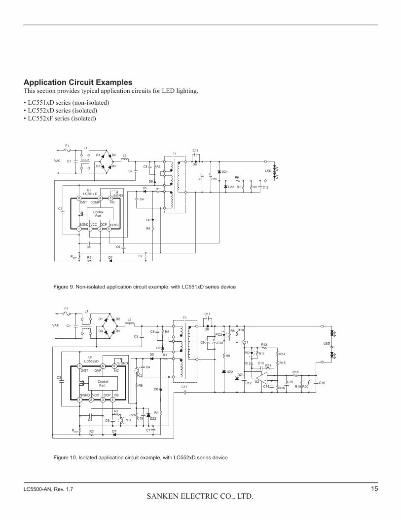
Application Circuit ExamplesThis section provides typical application circuits for LED lighting.
• LC551xD series (non-isolated)• LC552xD series (isolated)• LC552xF series (isolated)
5
1 2 3
D/ST8
S/GND VCC
ControlPart
C2
C5
D8
U1
D1
D3
D2
D4
F1L1
C1
D5
C4
DZ1
COMP
DZ2
D6
T1
C3
D7
L2
LED
OCP ISENSE
NC
R1
C6
D9
S/GND
ROCP R3
R4
R5
R6
R7
VAC
C8
C7
C9
C11
C12
LC551x D4
6
C10
R8
C2
C6 C18C5
D8
+
-
PC1
U2
DZ1
D1
D3
D2
D4
F1L1
C1
Q1
D5
C4
C3
T1
D6
D7
DZ2
DZ3
PC2
L2
LED
R1
PC2
D9
R8
R9
R10
R11
R12
R13
R14
R15
R16
R17
R18
R19 R20
ROCP R3
R4R21
R5
R6
VAC
PC1
R7
C7
C8
C10C9
C11
C12
C13
C14C15 C16
C17
5
1 2 3
D/ST8
S/GND VCC
ControlPart
U1
OVP
OCP FB
NC
S/GNDLC552xD6
4
Figure 9. Non-isolated application circuit example, with LC551xD series device
Figure 10. Isolated application circuit example, with LC552xD series device

16SANKEN ELECTRIC CO., LTD.
LC5500-AN, Rev. 1.7
Figure 11. Isolated application circuit example, with LC552xF series device
T1
C2
D1
D3
D2
D4
F1 L1
C1
D5
L2
D6
D9
D8
+-
PC1
U2DZ1
Q1
DZ2
DZ3
LED
PC2
C4
PC2
D7
R1
R8
R9
R10
R11
R12
R13
R14
R15
R16
R17
R18
R19
7OVP
R4
R5
R6
VAC
PC1
R7
C7
C8
C10
C11
C12
C13
C14C15 C16
C9
C17
Vcc
6OCP FB
C6
54VCC
3NCS/GND
2
R20
1D/ST
U1
C5
C3
ROCP R3
LC552xF
ControlPart
C18R21

17SANKEN ELECTRIC CO., LTD.
LC5500-AN, Rev. 1.7
Functional Description
All of the parameter values used in these descriptions are typi-cal values, unless they are specified as minimum or maximum. This section describes IC operations as it is used for LED lighting power supply applications. About current direction, "+" indicates sink current toward the IC and "–" indicates source current from the IC. The pin numbers parenthesized represent LC552xF num-bers.
On-Time Control OperationLC551xD series (non-isolated designs) Figure 12 shows the peripheral circuit at the COMP pin of the LC551xD, and figure 13 shows the on-time control. The output control is done by voltage mode control, which controls on-time depending on output load, and average current control.
As showed in figure 13, in the average current control operation, the output current detection resistor voltage is compared against the reference voltage, VSEN(TH) = 0.3 V, by the OTA circuit, and its output is averaged at COMP pin. This voltage is compared against the internal oscillator (OSC) by the FB comparator in order to control the on-time for the average current control opera-tion. Here, OSC indicates the oscillator circuit, which controls the PWM operation frequency, quasi-resonant oscillation, and the maximum on-time limit.
For the LC551xD devices, the recommended value of C6, which is connected to the COMP pin, is approximately 2.2 μF.
The value of R6 is approximately 1 kΩ.
The constant output current control of the output is done as below:
• When the output load current becomes less than the target value, the ISENSE pin voltage becomes low. This causes the averaged OTA circuit output voltage at the COMP pin to become high, which increases the on-time and the output current.
• When the output current becomes greater than the target value, the circuits operate in the opposite way. The averaged voltage at the COMP pin becomes low, and reductions result in the on-time and the output current.
Figure 14 shows the average input current waveform. The aver-aged COMP pin voltage becomes constant, and the duty cycle is controlled according to the EIN voltage (C2 voltage in figure 9). It makes an averaged input current sine waveform which realizes a high power factor.
LC552xD and LC552xF series (isolated designs) Figure 15 shows the peripheral circuit at the FB pin of the LC552xD/LC552xF, and figure 16 shows the on-time control. The output
Figure 13. On-time control, LC551xD series
1
–+
–+
4
6 R6
C6FB
OTA
LED Current
LC551xD
detection resistor
ISENSE
S/GND
COMP
COMP pinvoltage
Gate on-time
Gate on-time
Drain current
OSC
VCOMP OSC
31
COMP
R OCP
C6S/GND
ISENSE
D7
OCP
LC551xD
R3
6
4
Figure 12. COMP pin peripheral circuit

18SANKEN ELECTRIC CO., LTD.
LC5500-AN, Rev. 1.7
Figure 14. Averaged input current waveform, LC551xD series
COMP pin voltage
S/GND
EIN Drain current Averaged input current
1(2)
–+
–+
4(6)LED
Current detection resistor
S/GND
FB
C6
R7
FB pinvoltage
Gate on-time
Gate on-time
Drain current
OSC
VFB
OSC
PC
(LC552xF)LC552xD
control is done by voltage mode control, which controls on-time depending on output load, and average current control.
As showed in figure 16, in the average current control operation, the output current detection resistor voltage is compared by the operational amplifier, and its output is sent to the FB pin in con-junction with the opto-coupler and averaged at the FB pin. The FB pin voltage is compared against the internal oscillator (OSC) by the FB comparator in order to control the on-time for averaged current control operation. Here, OSC indicates the oscillator cir-cuit, which controls the PWM operation frequency, quasi-resonant oscillation, and the maximum on-time limit. For the LC552xD and LC552xF series devices, the recommended value of C6, which is connected to the FB pin, is approximately 2.2 μF.
The constant output current control of the output is done as below.
• When the output load current becomes less than the target value, the secondary current detection resistor voltage becomes low and it results in low feedback current from the opto-coupler. It causes the averaged voltage at the FB pin to become high, and results in increases of the on-time and the output current.
• When the output current becomes more than the target value, the circuits operate in the opposite way The averaged voltage at the FB pin becomes low, which reduces the on-time and the output current.
Figure 17 shows the average input current waveform. The aver-aged FB pin voltage becomes constant, and the duty cycle is controlled according to the EIN voltage (C2 voltage in figures 10 and 11). It makes an averaged input current sine waveform which realizes a high power factor.
Figure 15. FB pin peripheral circuit
3(5)1(2)
R OCP
S/GND
4(6)
D7
FB
C6PC1
OCP
R3
R7LC552xD
(LC552xF)
Figure 16. On-time control, LC552xD and LC552xF series

19SANKEN ELECTRIC CO., LTD.
LC5500-AN, Rev. 1.7
Figure 17. Averaged input current waveform, LC552xD and LC552xF series
FB pin voltage
S/GND
EIN Drain current Averaged input current
D/STVCC
S/GND
DV
PC2
2(4)
8(1)
C4
1(2)
D
L2
LC55xxD(LC552xF)
D5 R1
VCC pinvoltage
= 3.7mA ICC(ON) (max)
Sto
p
Sta
rtup
ICC
9.4 V VCC(OFF) VCC(ON)
15.1 V
Figure 18. VCC pin peripheral circuit
Figure 19. VCC versus operation current, ICC
Startup OperationFigure 18 shows the VCC pin peripheral circuit. The integrated startup circuit is connected to the D/ST pin. When the D/ST pin voltage reaches VSTARTUP = 57 V, the startup circuit is activated, and it generates a constant current, ICC(STARTUP) = –3.0 mA, to charge capacitor C4 at the VCC pin. During this process, when VCC voltage reaches VCC(ON) = 15.1 V, the IC starts operation, and when its voltage exceeds VCC(BIAS)2 = 16.6 V, the startup cir-cuit stops, in order to eliminate its own power consumption.
The startup time is determined by the C4 capacitance and is expressed by the formula below:
tSTART C4≈|ICC(STARTUP)|
VCC(ON) – VCC(INT)
(1)
wheretSTART is the startup time (s), andVCC(INT) is the VCC pin initial voltage (V).
A ceramic or film capacitor can be used for C4, and a value of 0.22 to 22 μF is generally recommended.
Figure 19 shows the relationship between VCC voltage and the operating current, ICC . When VCC voltage reaches VCC(ON) = 15.1 V, the Control circuit operation begins and the operating current increases. After that, if VCC voltage decreases to VCC(OFF) = 9.4 V, the Undervoltage Lockout (UVLO) circuit stops Control circuit operation, and the operation state returns to the startup phase.
After the IC starts operation, the rectified voltage from the auxil-iary winding, D, of figure 18 becomes a power source to the IC in steady-state operation.
VCC voltage must satisfy these conditions:VCC(BIAS)1(max) = 12.5 V < VCC < VCC(OVP)(min) = 28.5 V
Initially, target 20 V in a transformer design, and then optimize its winding turns in a way that VCC voltage stays within the above range over the conceivable input voltage range and output load conditions.

20SANKEN ELECTRIC CO., LTD.
LC5500-AN, Rev. 1.7
Figure 20 shows the VCC voltage behavior at the startup phase. Immediately after the Control circuit starts operation, the auxiliary winding voltage, VD , has not yet reached its design target value, which is determined by the transformer auxiliary winding turns. Therefore, as shown figure 20, VCC voltage starts decreasing after the startup circuit turns off at VCC(BIAS)2 = 16.6 V. If the VCC volt-age reaches VCC(BIAS)1 = 11.0 V, the bias assisting function is acti-vated before the voltage decreases to VCC(OFF) = 9.4 V. While the bias assist function is operating, any decrease of the VCC voltage is counteracted by a supplementary current from the startup circuit, and thus VCC is kept almost constant. Thanks to this function, the C4 value can be small, which results in shortening the startup period and improving the response time of the VCC pin overvolt-age protection. It is necessary to check and adjust the process so that poor starting conditions may be avoided.
In actual power supply circuits, there are cases in which the VCC pin voltage fluctuates in proportion to the output of the SMPS (see figure 21). This happens because C4 is charged to a peak voltage on the auxiliary winding D, which is caused by the tran-sient surge voltage coupled from the primary winding when the incorporated power MOSFET turns off.
For alleviating C4 peak charging, it is effective to add some value R1, of several tenths of ohms to several ohms, in series with D5 (see figure 22). The optimal value of R1 should be determined using a transformer matching what will be used in the actual application, because the proportion of the VCC pin voltage versus the transformer output voltage differs according to transformer structural design.
Fluctuation of VCC by IOUT worsens in the following cases, requir-ing a transformer designer to pay close attention to the placement of the auxiliary winding D:
• Poor coupling between the primary and secondary windings (this causes high surge voltage and is seen in a design with low output voltage and high output current).
▪ Poor coupling between the auxiliary winding D and the sec-ondary stabilized output winding where the output line voltage is controlled constant by the output voltage feedback (this is susceptible to surge voltage).
IOUT
VCC pinvoltage
With R1
Without R1
DVcc
D5
C4
2(4)
1(2)
LC55xxD(LC55xxF)
S/GND
R1
Added
Figure 21. VCC versus IOUT with and without resistor R1
Figure 22. VCC pin peripheral circuit with R1
Figure 20. VCC at startup period
Time
= 15.1 V
= 11.0 V
VCC pinvoltage
VCC(OFF)
VCC(ON)= 16.6 V VCC(BIAS)2
VCC(BIAS)1
= 9.4 V
Operation start
Startup successful Startup circuit off
Bias assist period
Startup failure
Increasing by outputvoltage rising

21SANKEN ELECTRIC CO., LTD.
LC5500-AN, Rev. 1.7
Figure 23. Transformer winding structures
P2 DP1 S1 S1 P1 S1 D P2S1
P1, P2: Primary Winding S1: Secondary Winding D: Auxiliary winding
Core
Bobbin
P1, P2: Primary WindingS1: Secondary WindingD: Auxiliary winding
Core
Bobbin
(A) (B)
Figure 23 shows two transformer design examples considered the winding location of the auxiliary winding D to minimize impact of VCC surge voltage. Triple insulation wires are used for either the primary or secondary winding, and thus no margin-tape is used:
• Separate the auxiliary winding D from the primary windings P1 and P2 (figure 23 (A)); P1 and P2 are two separated primary windings.
• Place the auxiliary winding D within the secondary winding S1 in order to improve the coupling of those windings (figure 23 (B)); S1 is the secondary output winding.

22SANKEN ELECTRIC CO., LTD.
LC5500-AN, Rev. 1.7
Operation Modes at StartupFigure 24 shows the operation modes during the startup phase of the LC551xD, and figure 25 shows those for the LC552xD and LC552xF. Note that OCP pin voltage, which determines the tim-ing of quasi-resonant operation, is in positive voltage on the OCP pin, in reference to the S/GND pin.
During two periods below at startup, IC operation is set to PWM, with fOSC = 14 kHz:
• While the COMP pin voltage (for LC551xD) and FB pin volt-age (for LC552xD and LC552xF), in reference to S/GND, are 0 to 0.9 V (the control voltage lower limit for the COMP pin, VCOMP(MIN), and FB pin, VFB(MIN) ): During this period, on-time is fixed at the Leading Edge Blanking Time, tBW = 500 ns.
• Until the quasi-resonant signal (OCP pin voltage) reaches the Quasi-Resonant Operation Threshold Voltage-1, VBD(TH1) = 0.24 V: During this period, the output voltage is low; therefore, the auxiliary winding voltage, VD , is low. Thus the quasi-reso-nant signal is low.
After those startup operations the output voltage starts increasing, when the OCP pin voltage reaches VBD(TH1) = 0.24 V, the IC is switched to quasi-resonant operation (figure 26).
Soft-Start FunctionThe soft-start function reduces power stress on the incorporated MOSFET and secondary rectifier during the startup phase.
LC551xD series (non-isolated designs) The soft-start operation begins when the COMP pin voltage reaches VCOMP(MIN) = 0.9 V and lasts until the output current becomes constant. During that period, the output power gradually increases.
During this period, check the items below:
• VCC pin voltage does not drop to the Operation Stop Voltage, VCC(OFF)
• Output current reaches the target value before the overload pro-tection (OLP) is activated by the COMP pin voltage reaching VCOMP(OLP)2 = 4.5 V
VCC Pin Voltage
COMP Pin Voltage
Output (LED) Current, IOUT
Drain Current, ID
S/GND
IC turn on
S/GND
GND(IOUT)
Duration
PWM (QR)
VCOMP(MIN) = 0.90 V
VCC(BIAS 1) = 11.0 V
Soft-Start Period
TargetCurrent
GND(ID )
Constant current operation
tON= tBW(500 ns)
VCC Pin Voltage
FB Pin Voltage
Output (LED) Current, IOUT
Drain Current, ID
S/GND
IC turn on
S/GND
GND(IOUT)
Duration
PWM (QR)
VFB (MIN) = 0.90 V
VCC(BIAS 1) = 11.0 V
Soft-Start Period
TargetCurrent
GND(ID )
Constant current operation
tON= tBW(500 ns)
Figure 24. Soft-start operation waveforms at startup (LC551xD) Figure 25. Soft-start operation waveforms at startup (LC552xD/ LC552xF)
GND(ID)
S/GND
VBD(TH1)
PWM operation Quasi-resonant operation (QR)
OCP Pin Voltage
Drain Current, ID
Figure 26. OCP Pin Voltage (with time scale expanded)
23SANKEN ELECTRIC CO., LTD.
LC5500-AN, Rev. 1.7
LC552xD/LC552xF series (isolated designs) The soft-start oper-ation begins when the FB pin voltage reaches VFB(MIN) = 0.9 V and lasts until the output current becomes constant. During that period, the output power gradually increases.
During this period, check the items below:
• VCC pin voltage does not drop to the Operation Stop Voltage, VCC(OFF)
• Output current reaches the target value before the overload protection (OLP) is activated by the FB pin voltage reaching VFB(OLP)2 = 4.5 V
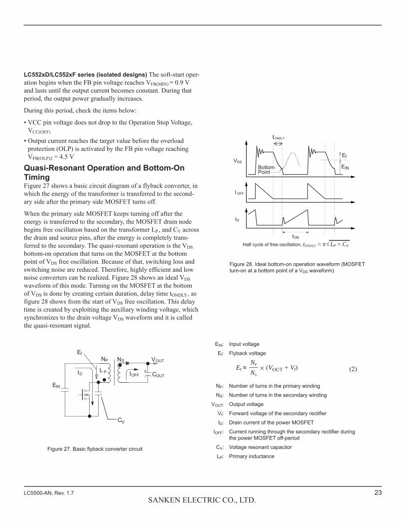
Quasi-Resonant Operation and Bottom-On TimingFigure 27 shows a basic circuit diagram of a flyback converter, in which the energy of the transformer is transferred to the second-ary side after the primary side MOSFET turns off.
When the primary side MOSFET keeps turning off after the energy is transferred to the secondary, the MOSFET drain node begins free oscillation based on the transformer LP , and CV across the drain and source pins, after the energy is completely trans-ferred to the secondary. The quasi-resonant operation is the VDS bottom-on operation that turns on the MOSFET at the bottom point of VDS free oscillation. Because of that, switching loss and switching noise are reduced. Therefore, highly efficient and low noise converters can be realized. Figure 28 shows an ideal VDS waveform of this mode. Turning on the MOSFET at the bottom of VDS is done by creating certain duration, delay time tONDLY , as figure 28 shows from the start of VDS free oscillation. This delay time is created by exploiting the auxiliary winding voltage, which synchronizes to the drain voltage VDS waveform and it is called the quasi-resonant signal.
Figure 27. Basic flyback converter circuit
EIN
IOFF
VOUT
ID
EfNP
P
NS
CV
L COUT
EIN: Input voltage
Ef: Flyback voltage
Ef (VOUT + Vf)=NP
NS(2)
NP: Number of turns in the primary winding
NS: Number of turns in the secondary winding
VOUT: Output voltage
Vf: Forward voltage of the secondary rectifier
ID: Drain current of the power MOSFET
IOFF: Current running through the secondary rectifier duringthe power MOSFET off-period
CV: Voltage resonant capacitor
LP: Primary inductance
Figure 28. Ideal bottom-on operation waveform (MOSFET turn-on at a bottom point of a VDS waveform)
EIN
ONDLYt
BottomPoint
Ef
I OFF
DI
tON
VDS
Half cycle of free oscillation, tONDLY ≈ √ LP × CV

24SANKEN ELECTRIC CO., LTD.
LC5500-AN, Rev. 1.7
Figure 29 shows the OCP pin peripheral circuit. D6, R4, C7 and D7 form a delay circuit, and the auxiliary winding flyback volt-age, Erev1 , is fed through the delay circuit and provides positive voltage, the quasi-resonant signal (VBD), to the OCP pin. Fig-ure 30 shows the auxiliary winding voltage and quasi-resonant signal.
After the power MOSFET turns off, the quasi-resonant signal immediately goes up and it exceeds the Quasi-Resonant Opera-tion Threshold Voltage-1, VBD(TH1) = 0.24 V. After this occurs, the power MOSFET remains off until the quasi-resonant sig-nal comes down enough to cross the Quasi-Resonant Opera-tion Threshold Voltage-2, VBD(TH2) = 0.17 V. Then the power MOSFET again turns on. In addition, at the point, the threshold voltage goes up to VBD(TH1) automatically to prevent malfunction of the quasi-resonant operation from noise interference..
During that period, C7 must cause a delay time, tONDLY , such that the power MOSFET turns on at the bottom point of VDS ; so select an appropriate C7 value. R3 is recommended to be between 100 and 330 Ω, and C5 to be between 100 and 470 pF.
R4 must set the range for the quasi-resonant signal: greater than or equal to VBD(TH1) under input and output conditions where VCC becomes lowest, but less than the OCP Pin Overvoltage Protec-tion (OVP) Threshold Voltage, VBD(OVP) = 2.6 V, under conditions where VCC becomes highest. Figure 31 defines the pulse width of the quasi-resonant signal. For initiating quasi-resonant operation, the quasi-resonant signal pulse width between the two points VBD(TH1) and VBD(TH2) , tQR, must be equal to 1.2 μs or more. This pulse width must be ensured, while at the same time the OCP pin peak voltage, VBD(PK) , is recommended to be between 1.5 and 2.0 V. Both conditions should be satisfied throughout the power sup-ply input and output ranges, over variations in R3 and R4 actual component values.
Figure 29. OCP pin peripheral circuit
Figure 30. Auxiliary winding voltage and quasi-resonant signal
Pulse width, tQR ≥ 1.2μs
S/GND
VBD(PK), 1.5 to 2.0 V recommended, but less than 2.6 V
VBD(TH1) = 0.34 V (max)
VBD(TH2 ) = 0.22 V (max)
Figure 31. Definition of the pulse width of the quasi-resonant signal
8(1)
S/GND
VCCD/ST
OCP 3(5)
2(4)
C2
D5 R1
C4
T1
D
P
ROCP
C3
R4
D6
C7
EIN EF
EIN
Flyback voltageForward voltage
Clamping snubber
1(2)
C5R3
D7LC5500
VBD
Erev1 Efw1
0
Efw1
Erev1
tON
D
VBD(TH1)VBD(TH2)
0
Quasi-resonant signal
VBD
Auxiliarywinding voltage
V

25SANKEN ELECTRIC CO., LTD.
LC5500-AN, Rev. 1.7
Because ROCP is much less than R3, the formula below is used to calculate R4:
R4 =R3 (VCC – VBD(PK) – 2Vf )
VBD(PK) (3)
given R3 = 220 Ω, VBD(PK) = 1.5 V, VCC = 16 V, and the Vf of D6 and D7 = 0.8 V. R4 is approximately 1.89 kΩ, and it is 1.8 kΩ in the E12 series.
If the pulse width is not satisfied, increase R3 or decrease R4, in order to raise VBD(PK) . Alternatively, increasing the capacitance of resonant capacitor C3 is also effective because it widens the free oscillation period. However, it causes an additional switching loss increase; therefore, ensure the IC temperature rise is acceptable.
Figure 32 shows two different OCP pin waveforms, comparing transformer coupling conditions between the primary and second-ary winding. The poor coupling tends to happen in a low output voltage (small number of LEDs) transformer design with high NP / NS turns ratio (NP and NS indicate the number of turns of the primary winding and secondary winding, respectively), and it results in high leakage inductance. The poor coupling causes high surge voltage ringing at the power MOSFET drain pin when it turns off. That high surge voltage ringing is coupled to the auxil-iary winding and then the inappropriate quasi-resonant signal, as in figure 32B, is created. The OCP pin has a blanking period of
250 ns (max) to avoid reacting to it, but if the surge voltage con-tinues longer than that period, the IC responds to it and repeat-edly turns the power MOSFET on and off at high frequency. This results in an increase of the MOSFET power dissipation and temperature, and it can be damaged.
If this phenomenon is observed, countermeasures include:
• Place C5 as close to the OCP and S/GND pins as possible• Separate the loop trace between the OCP pin and the S/GND
pin from any high current trace• Loosen the transformer coupling between the auxiliary winding
and primary winding• Reinforce the clamping snubber circuit to reduce the surge
voltage
In addition, the OCP pin waveform during operation should be measured by connecting test probes with leads to the OCP pin and the GND pin as short as possible, in order to measure any surge voltage correctly.
Timing adjustment of the bottom-on is done by selecting the value of C7 (figure 29). To do so, observe the power MOSFET drain voltage, VDS , the drain current, ID , and the quasi-resonant signal. Then optimize the C7 value to adjust the delay time of tONDLY so that the MOSFET turns on at the bottom point of VDS.
Figure 32. The difference of OCP pin voltage waveform by the coupling condition of the transformer; good coupling (left) versus inappropriate coupling (right)
(A) Proper OCP Voltage, Erev2
VBD(TH1)= 0.24 V
VBD(TH2) = 0.17 V
S/GNDOCP pin blanking time, 250 ns (max)
(B) Inappropriate OCP Voltage, Erev2

26SANKEN ELECTRIC CO., LTD.
LC5500-AN, Rev. 1.7
As shown in figure 33:• If the turn-on point is earlier than the bottom of the VDS signal,
it causes higher switching losses. In that situation, delay the turn-on point by increasing the C7 value.
• In the converse situation, if the turn-on point is later than the VDS bottom point, it also causes higher switching losses, but in that case, advance the turn-on point by decreasing the C7 value. An initial reference value for C7 is about 1000pF.
Latch FunctionThermal shutdown (TSD) protection is latched. When the latch circuit is activated, the IC stops switching operation, and there-fore the VCC voltage declines.
However, the startup circuit turns on again when VCC reaches VCC(BIAS)1 = 11.0 V, in order to avoid reaching the operation stop-ping voltage, VCC(OFF) = 9.4 V. Thus IC operation in latch mode
Figure 33. Effects of failure to turn on precisely at the VDS bottom point: (left) turn-on before a bottom point, (right) turn-on after a bottom point
IOFF
VDS
tON
ID
S/GND S/GND
tON
AuxiliaryWinding Voltage
IOFF
VDS
ID
OCP pinvoltage
OCP pinvoltage
AuxiliaryWinding Voltage
S/GND VBD(TH2)
VBD(TH1)
S/GND VBD(TH2)
VBD(TH1)
VDS
VDS(peak)2 × AC mains frequency
AC mains frequency (50 Hz / 60 Hz)
Early turn-on point Delayed turn-on point
EIN(max)
GND
fR ≈ 2 √ LP × CV
1
Bottom point Free oscillation, fR Bottom point Free oscillation, fR
Turn-on occurring after the VDS bottom pointTurn-on occurring before the VDS bottom point

27SANKEN ELECTRIC CO., LTD.
LC5500-AN, Rev. 1.7
is maintained. To release the IC from latch mode, cut off the AC mains and let VCC voltage drop below VCC(OFF).
Overvoltage Protection (OVP)LC551xD series (non-isolated designs) The LC551xD series has three OVP activation methods link to the VCC pin, to the OCP pin, and to the ISENSE pin:
• VCC Pin Overvoltage Protection. figure 34 shows the wave-forms of the OVP function on the VCC pin. When the VCC pin voltage with reference to the S/GND pin reaches and exceeds VCC(OVP) = 31.5 V, OVP is activated and the IC stops switching operation. During this function, the bias assist function is dis-
abled, and the VCC voltage decreases to VCC(OFF) = 9.4 V. After that, the startup circuit is activated, and the operation begins intermittent operation by repeating the restart and operation pro-cess as long as the OVP condition remains.
In addition, because VCC voltage is proportional to the output voltage, it can be used to detect an output overvoltage event, such as open load condition. In this situation, the detecting voltage is expressed by the formula below:
=VOUT(OVP) 31.5 (V)VCC(normal operation)
VOUT(normal operation)
(4)
Figure 34. Waveforms when VCC pin OVP is being activated (LC551xD)
COMP pinvoltage
Drain current, ID
VCC pinvoltage

28SANKEN ELECTRIC CO., LTD.
LC5500-AN, Rev. 1.7
• OCP Pin Overvoltage Protection. Figure 35 shows the OCP pin OVP function. When the OCP pin voltage with reference to the S/GND pin reaches VBD(OVP) = 2.6 V or more, OVP is activated. This input voltage must be less than the absolute maximum rat-ing, 5V.
During this function, the bias assist function is disabled, and thus the IC enters intermittent operation as described in the VCC pin OVP section, above. This can be used as protection in the event that the quasi-resonant signal setup is mistaken or excess load current happens in the use of a poor coupling transformer between the primary and secondary winding.
• ISENSE Pin Overvoltage Protection. Figure 36 shows the ISENSE pin OVP operation. When the ISENSE pin voltage with reference to the S/GND pin reaches and exceeds VSEN(OVP) = 2.0 V or more, OVP is activated. This input voltage must be less than the absolute maximum rating, 5V.
During this function, the bias assist function is disabled, and thus the IC enters intermittent operation as described in the VCC pin OVP section, above. As shown in figure 9, with Zener diode DZ1 this function can be used to detect an excess output voltage, such as caused by an open load condition, and protect the circuit.
Figure 36. Waveforms when ISENSE pin OVP is being activated (LC551xD)
Draincurrent, ID
VCC pinvoltage
VBD(OVP)= 2.6V
VCC(ON)= 15.1VVCC(OFF)= 9.4V
OCP pinvoltage
COMP pinvoltage
VCC pinvoltage VCC(ON)= 15.1V
VCC(OFF)= 9.4V
Drain current, ID
VCOMP(MIN)= 0.90V
ISENSE pinvoltage
VSEN(OVP) = 2.0V
tON= tON(LEB)(500ns)
Figure 35. Waveforms when OCP pin OVP is being activated (LC551xD)

29SANKEN ELECTRIC CO., LTD.
LC5500-AN, Rev. 1.7
LC552xD/LC552xF series (isolated designs) The LC552xD and LC552xF series have three OVP activation methods link to the VCC pin, to the OCP pin, and to the OVP pin:
• VCC Pin Overvoltage Protection. figure 37 shows the wave-forms of the OVP function. When the VCC pin voltage with ref-erence to the S/GND pin reaches and exceeds VCC(OVP) = 31.5 V or more, OVP is activated and the IC stops switching operation.
During this function, the the bias assist function is disabled, and the VCC voltage decreases to VCC(OFF) = 9.4 V. After that, the startup circuit is activated, and the operation begins intermittent operation by repeating the restart and operation process as long as the OVP condition remains. In addition, because VCC voltage is proportional to the output voltage, it can be used to detect output overvoltage events, such as open load condition. In this situation, the detecting voltage is expressed by equation 4.
Figure 37. Waveforms when VCC pin OVP is being activated (LC552xD and LC552xF)
FB pin voltage
VCC pinvoltage
VCC(OVP)= 31.5V
VCC(ON)= 15.1VVCC(OFF)= 9.4V
Drain current, ID
VFB(MIN)= 0.90V
tON= tON(LEB)(500ns)

30SANKEN ELECTRIC CO., LTD.
LC5500-AN, Rev. 1.7
Figure 39. Waveforms when OVP pin OVP is being activated (LC552xD and LC552xF)
Drain current, ID
VCC pinvoltage
VBD(OVP) = 2.6V
VCC(ON)= 15.1VVCC(OFF)= 9.4V
OCP pinvoltage
Figure 38. Waveforms when OCP pin OVP is being activated (LC552xD and LC552xF)
FB pinvoltage
VCC pinvoltage
VCC(ON)= 15.1VVCC(OFF)= 9.4V
Drain current, ID
VFB(MIN)= 0.90V
OVP pinvoltage
VOVP(OVP) = 2.0V
tON= tON(LEB)(500ns)
• OCP Pin Overvoltage Protection. Figure 38 shows the OCP pin OVP function. When the OCP pin voltage with reference to the S/GND pin reaches VBD(OVP) = 2.6 V, OVP is activated. This input voltage must be less than the absolute maximum rating, 5V.
During this function, the bias assist function is disabled, and thus the IC enters intermittent operation as described in the VCC pin OVP section, above. This can be used as protection in the event the quasi-resonant signal setup is mistaken or excess load current happens in the use of a poor coupling transformer between the primary and secondary winding.
• OVP pin Overvoltage Protection. Figure 39 shows the OVP pin OVP function. When the OVP pin voltage with reference to the S/GND pin reaches and exceeds VOVP(OVP) = 2.0 V, OVP is acti-vated. This input voltage must be less than the absolute maximum rating, 5V.
During this function, the bias assist function is disabled, and thus the IC enters intermittent operation as described in the VCC pin OVP section, above.. As shown in figure 10 and figure 11, with PC2 this function can be used to detect high output voltage, such as an open load condition.

31SANKEN ELECTRIC CO., LTD.
LC5500-AN, Rev. 1.7
Overload Protection (OLP)If the MOSFET drain current is limited by the overcurrent pro-tection for a certain delay period, tDLY , Overload Protection is activated and the IC enters intermittent oscillation mode opera-tion. This reduces the power-up stress on the incorporated power MOSFET and secondary rectifier.
LC551xD series (non-isolated designs) Figure 40 shows the peripheral circuit at the COMP pin, and figure 41 shows opera-tion when OLP is activated.
At an overload condition, the output voltage, the VCC pin volt-age, and the ISENSE pin voltage drop. When the VCC pin volt-age reaches VCC(BIAS)1 = 11.0 V, the bias assist function is enabled in order to avoid reaching VCC(OFF) = 9.4 V. When the ISENSE
pin voltage reaches VSEN(TH) = 0.30 V, the output of the OTA circuit becomes zero, and therefore the internal constant current source at the COMP pin starts charging capacitor C6.
When the COMP pin voltage reaches Overload Protection Threshold Voltage-2, VCOMP(OLP)2 = 4.5 V, the on-time is set to the Leading Edge Blanking time, tON(LEB) = 500 ns. Meanwhile, the capacitor charging is ongoing and when it reaches Overload Protection Threshold Voltage-1, VCOMP(OLP)1 = 5.5 V, the switch-ing operation stops and the VCC voltage decreases to VCC(OFF) = 9.4 V.
After that, the startup circuit is activated. Thus, the operation begins intermittent operation by repeating the restart and opera-tion stop processes as long as the overload condition remains.
Figure 40. COMP pin peripheral circuit
Figure 41. Waveforms when OLP is being activated (LC551xD)
VCOMP(OLP)2= 4.5VVCOMP(OLP)1= 5.5V
COMP pinvoltage
VCC pinvoltage
VCC(ON)= 15.1V
Drain current, ID
tON= tON(LEB)(500ns)
VCC(BIAS)1= 11.0VVCC(OFF)= 9.4V
VCOMP(MIN)= 0.90V

32SANKEN ELECTRIC CO., LTD.
LC5500-AN, Rev. 1.7
LC552xD/LC552xF series (isolated designs) Figure 42 shows the peripheral circuits at the FB pin of the LC552xD/LC552xF series and figure 43 shows the waveforms when the Overload Protection (OLP) is activated. At an overload condition, the out-put voltage drops. When the VCC pin voltage reaches VCC(BIAS)1 = 11.0 V, the bias assist function is enabled in order to avoid reaching VCC(OFF) = 9.4 V. At the time, a feedback signal from the secondary output becomes zero, and the PC1 is cut off. Thus, the feedback current from the FB pin charges the C6 capacitor, and the FB pin voltage increases.
When the FB pin voltage reaches the Overload Protection Threshold Voltage-2, VFB(OLP)2 = 4.5 V, the on-time is set to Leading Edge Blanking time, tON(LEB) = 500 ns. In the mean-while, the capacitor charging is ongoing and when it reaches at Overload Protection Threshold Voltage-1, VFB(OLP)1 = 5.5 V, the switching operation stops and the VCC voltage decreases to VCC(OFF) = 9.4 V.
After that, the startup circuit is activated. Thus, the operation begins intermittent operation by repeating the restart and opera-tion stop processes as long as the overload condition remains.
Figure 42. FB pin peripheral circuit
Figure 43. Waveforms when OLP is being activated (LC552xD/ LC552xF)
VFB(OLP)2= 4.5VVFB(OLP)1= 5.5V
FB pinvoltage
VCC pinvoltage
VCC(ON)= 15.1V
Draincurrent, ID
tON= tON(LEB)(500ns)
VCC(BIAS)1= 11.0VVCC(OFF)= 9.4V
VFB(MIN)= 0.90V
7VReg
ROCP
S/GND OCP1(2)
4(6)
FB
C6PC1
LC552xD R7(LC552xF)
3(5)

33SANKEN ELECTRIC CO., LTD.
LC5500-AN, Rev. 1.7
Overcurrent Protection (OCP)The Overcurrent Protection (OCP) feature monitors the power MOSFET drain current on a pulse-by-pulse basis, in order to limit output power. The drain current is detected by a current detection resistor, ROCP , and the voltage across it, VROCP , is fed through R3 to the OCP pin to be detected by it. When the ROCP voltage, VROCP , reaches the value of the following formulas, the power MOSFET turns off.
= –VROCP |VOCP | + R3 |IOCP |
(5)
where VOCP: Overcurrent Detection Threshold Voltage, –0.60 V, R3: R3 Resistance, and IOCP: OCP Pin Source Current, –40 μA.
In order to minimize effects of variation in the internal resis-tor, R3 (figure 44) is recommended to have a value from 100 to 330 Ω. and C5 is recommended to have a value from 100 to 470 pF, with good temperature characteristics. Selecting larger capacitances slows OCP response, and results in an increase in the drain current peak at transient conditions, such as start-up.
Because the OCP function is designed for peak current detection, there is a chance that it will react to the surge current at the power MOSFET turn-on edge. In order to avoid this, the Leading Edge Blanking Time, tON(LEB) , = 500 ns, is set.
The surge voltage pulse width must be less than tON(LEB) as shown in figure 45. In case its width is longer than that, try these mea-sures:
• adjust the turn-on point to the VDS bottom point• reduce the voltage resonant capacitor CV (C3 in figure 44)
capacitance• reduce the secondary rectifier snubber capacitor capacitance
With the quasi-resonant converter, the peak drain current at the same output load condition becomes different in a universal AC input voltage range (85 to 265 VAC), that is, when the AC input voltage is high, the peak drain current is low because the opera-tion frequency becomes high.
When the OCP threshold voltage is fixed constant, the output cur-rent, IOUT , in an OCP operation increases according to an increase of AC input voltage, as shown in (A) IOUT without input compen-sation of figure 46.
In the maximum AC input voltage range, in order to control output current at OCP operation, IOUT(OCP) , an external OCP input compensation circuit (DX1, DZX1, RX1) is added as shown in figure 47. For more details as to how to set it, refer to the next section, Input Compensation Function for Overcurrent Protection.
Surge pulse voltage width at turning on
OCP detection period
S/GND
tON(LEB)
VROCP
Figure 44. OCP circuit for negative side detect
Figure 45. OCP pin voltage, converted from MOSFET drain current by ROCP
Figure 46. Input compensation OCP circuit: (A) IOUT without input compensation; (B) IOUT with appropriate input compensation; (C) with inappropriately set input compensation, more than enough amount of compensation, IOUT cannot meet target
AC Input Voltage (V)
A
C
B
85 265
Out
put C
urre
nt a
t OC
P, I O
UT(
OC
P)
IOUT target output level
+-
8(1)
1(2)
3(5)
V
Rocp
Rocp
LogicControl Part
Drive
OCP Comparator
−0.6V
C5
R3
C3
PC2D/ST
S/GND
OCP
Reg
Filter
LC55xxD (LC55xxF)

34SANKEN ELECTRIC CO., LTD.
LC5500-AN, Rev. 1.7
ROCPIOCP
Compensation Current, I
ID
C2
Forward voltage Efw1
NP NS
ND
D5 R1
S/GND OCP
D/ST
C5 1(2) 3(5)
8(1)
R3
D7
C7 D6
C4
R4 DX1
DZX1
RX1
Flyback voltage Erev1
LC55xxD (LC55xxF)
P S
D
EIN
Figure 48. OCP input compensation circuit
Figure 49. Efw1 and Efw2 voltage relative to AC input voltage
D/STVCC
S/GND
ROCP
R1
R3
C4
8(1)
2(4)
3(5)1(2)
PC2
C3
C5
LC55xxD(LC55xxF)
OCP
L2
D5
D6
C7D7
DX1
DZX1
RX1
R4
D
Figure 47. Input compensation OCP circuit
}
AC Input Voltage = 100 VAC Input Voltage = 230 V
Time
Time
Aux
iliar
y W
indi
ngFo
rwar
d Vo
ltage
Efw1
0
0
DZX1
OCP input compensationstarting point: Efw1 ≈ DZX1
Efw2
Input Compensation Function for Overcurrent ProtectionThe auxiliary winding forward voltage Efw1 is proportional to the input voltage, EIN . Efw1 is applied to DZX1 , and RX1 and R3 translate the voltage Efw1 – Zener voltage of DZX1 , into the input Compensation Current, I.
This input Compensation Current, I, creates the voltage of R3 × I, and it lowers the absolute value of the compensated OCP thresh-old voltage to less than the original OCP threshold voltage, VOCP = –0.6 V. This way, when EIN is high, the compensation amount becomes high.
The DZX1 Zener diode is used to set the voltage at which the input compensation begins, so choose the Zener voltage value that is equal to Efw1 at the time when input compensation begins.
Optimize the circuit in a way to minimize the difference between the overcurrent points at low and high AC input voltage. Also ensure that the output current meets its target over the entire AC input voltage range, as the normal curve shown in figure 46. The OCP pin voltage, including surge voltage, must not exceed its absolute maximum rating of –2.0 to 5.0 V at the highest AC input voltage.
OCP Threshold Voltage with and without the OCP Input Compensation CircuitWithout the input compensation circuit, as shown in the figure 50 upper panel, the overcurrent detecting voltage is equal to the sum of the Overcurrent Protection Threshold Voltage, VOCP = −0.60 V, and the voltage across R3 from the OCP pin source current, IOCP = – 40 μA.
= –VROCP |ROCP × IDP| = – |VOCP | + R3 × |IOCP |
(6)
In the converse situation, with the input compensation circuit, as shown in the figure 50 lower panel, the overcurrent detecting voltage is equal to the sum of the Overcurrent Protection Thresh-old Voltage, VOCP = −0.60 V, the voltage across R3 from the OCP pin source current, IOCP , and the voltage across R3 from the input Compensation Current, I :
= –V 'ROCP |VOCP | + R3 ×| IOCP | – R3 × I
(7)
• Determining OCP pin input compensation circuit component values
Given: EIN(PK) = C2 voltage IDP = MOSFET peak drain current VFX1 = DX1 forward voltage VZX1 = DZX1 Zener voltage

35SANKEN ELECTRIC CO., LTD.
LC5500-AN, Rev. 1.7
1. The overcurrent detecting peak drain current, IDP(OCP) , without the input compensation circuit, is expressed by the following, based on equation 6, from figure 50, upper panel:
=IDP(OCP) ROCP
|VOCP| + R3 × |IOCP|
(8)
2. On the other hand, the overcurrent detecting peak drain current, I'DP(OCP) , with the input compensation circuit, is expressed by the following, based on equation 7, from fig-ure 50, lower panel:
=I 'DP(OCP) ROCP
|VOCP| + R3 × (|IOCP| – I )
(9)
I'DP(OCP) is set to the peak drain current where the output cur-rent is equal to that at the maximum AC input voltage of the curve B in figure 46 (appropriate input compensation).
3. From equations 8 and 9, the compensation current, I, of the input compensation circuit, is expressed as follows:
( |I DP(OCP) | – |I 'DP(OCP)| )I = × ROCP R3
(10)
4. The forward voltage, Efw1 , at C2 peak voltage EIN(PK)(max) is expressed as follows:
NP
ND × EIN(PK)(max)=Efw1
(11)
5. Next, RX1 is expressed by the following, in order to let the
compensation current, I, flow at the maximum AC input volt-age, EIN(PK)(max):
Efw1 – VZX1 – VFX1
RX1 + R3 + ROCP=I
(12)
assuming: R3, ROCP << RX1
I
Efw1 – VZX1 – VFX1=RX1
(13)
from equations 11 and 13:
–
I
(VZX1 + VFX1 )
=NPRX1
ND × EIN(PK)(max)
(14)
• AC input compensation circuit design example with universal
inputHere is an example of design specification and calculation:
Given: AC input voltage: 85 to 265 VAC Output power: 40 W Transformer primary winding: 40 T Transformer auxiliary winding: 6 T ROCP = 0.2 Ω R3 = 220 Ω DX1 forward voltage: 0.8 V Tentatively, OCP input compensation start voltage, VIN(OCP_ST) ,
is set to the voltage of 100 to 130 VAC. At this time, VIN(OCP_ST) is set to 120 VAC.
Figure 50. Compensated drain current waveforms
R3R3
R3
×ROCP×IDP
R3 ×
IDP
Increase
Decrease
ROCP
IOCP
IOCP
I
IOCP
× I× IOCP
IDP
ID
ID
IDP
×
R3 ×
R3 ×
ROCP×
R3
VOCP
VOCP
R3
ROCP × IDP'
IDP' IDP' IDP'
S/GND
OCP
ROCP R3 RX1
ROCP
ROCP
ROCP
R3
S/GND
S/GND OCP
1(2)
1(2)
With inputcompensationcircuit
Without inputcompensationcircuit
VOCP
3(5)
3(5)
VOCP
VOCP
VOCP
IOCP
IOCP I
S/GND

36SANKEN ELECTRIC CO., LTD.
LC5500-AN, Rev. 1.7
1. Calculate Efw1 at 120 VAC input:
=Efw1 NP
ND
=
× EIN(PK)(max)
NP
ND × VIN(OCP_ST) × √2
= =406
× 120 25.5 (V)√2
(15)
Thus, select 27 V as the Zener value for DZX1.Assuming:IDP(OCP) , Drain current during OCP operation, measured at
EIN(min) of 85 VAC: 3.0 AI'DP(OCP) , Drain current when the output current is equal to that
at the maximum AC input voltage of the curve B in figure 46 (appropriate input compensation): 1.9 A
2. The compensation current, I, is calculated using equation 10:
=I 0.2 (Ω)220 (Ω)
= 1 (mA)(3.0 (A) – 1.9 (A)) ×
3. RX1 can be calculated using equation 14:
=
=
RX140 (T)
1 (mA)
28.4 (kΩ)
6 (T) × 265 (VAC)√2 – (27 (V) + 0.8 (V))
Thus, select RX1 = 27 kΩ out of the E12 series.
Finally, ensure that the output current limited by OCP operation is similar to that of the curve B in fi gure 46 (appropriate input compensation), in actual operation throughout AC input voltage ranges. If necessary, readjust the rating of DZX1 and RX1 by changing the compensation startup voltage VIN(OCP_ST) for OCP pin input voltage.
Thermal Shutdown ProtectionThermal Shutdown protection is activated when the temperature of the control circuit in the IC reaches Tj(TSD) = 135°C(min), and then the IC stops switching operation in latch mode.
Maximum On-Time Limiting FunctionThe maximum on-time, set at tON(MAX) = 40 μs (figure 51), limits lower side operation frequency, and it minimizes audible noise from the transformer, as well as power stress on the incorporated MOSFET and secondary rectifier at low AC input or during tran-sient periods such as at switching AC mains on or off.
Ensure that the actual on-time at the minimum AC input and the maximum load condition does not reach tON(MAX) = 40 μs. If that does happen, redesign the transformer, such as by reducing the
primary inductance or reducing the duty cycle by lowering the turns ratio of NP / NS .
Design Notes
Peripheral ComponentsTake care to use properly rated and proper type of components.
• Output smoothing capacitor. Consider design margins for rat-ings of ripple current, voltage, and temperature in selecting the output capacitor. A low impedance capacitor, designed to be tolerant against high ripple current, is recommended.
• Transformer. Consider design margins for temperature rise, resulting from copper losses and core losses, in designing or selecting a transformer.
Switching current contains a high frequency component that causes the skin effect; therefore, consider a current density of 3 to 4 A/mm2 and select a wire gauge based on RMS current.
In the event further temperature measurement is necessary, try the following measures to increase the surface area of the wire:▫ Increase the quantity of parallel wires▫ Use litz wire▫ Increase the diameter of the wires
• Current detection resistor, ROCP . Choose a low equivalent series inductance and high surge tolerant type for the current detec-tion resistor. If a high inductance type is used, it may cause malfunctioning because of the high frequency current running through it.
Transformer DesignIn this section, the pin symbol COMP/FB pin shows instead of COMP pin for the LC551xD and FB pin for the LC552xD/LC552xF.
ID
VDS
time
time
Maximum On-Time
Figure 51. Confirmation of Maximum On-Time

37SANKEN ELECTRIC CO., LTD.
LC5500-AN, Rev. 1.7
Figure 52 shows an ideal waveform in average current control relative to a sine wave of AC input voltage. The Average Current Control function controls COMP/FB pin voltage at a fixed rate relative to the sine wave of AC input voltage, VIN , at commercial frequencies. Therefore, the envelope curve of the peak drain cur-rent, IDP , and the input current, IIN (which is the averaged IDP ), shows a sine waveform which is similar to that of the AC input voltage.
To set the fixed COMP/FB pin voltage, the value of C6 and the constant current detection resistor must be be adjusted.
The transformer design is the same as for an RCC (ringing choke converter, or self-oscillation flyback converter) transformer design. However, a quasi-resonant operation includes a certain delay to turn-on, so duty cycle must be compensated. Moreover, for input capacitorless applications, the applied voltage of a trans-former is the sine wave of the AC input voltage, VIN , at commer-cial frequencies.
Therefore, the duty cycle compensation for quasi-resonant delay time is added to the basic equation of the RCC topology; more-over, the equation must be changed into the sine wave of the AC input voltage, VIN.
In consideration of quasi-resonant delay time, the primary side inductance, L'P , applied the sine wave of AC input voltage, is expressed by the following equation:
=L'P2 × POUT × fS(MIN)
( VINRMS(MIN) × DON )2
+ VINRMS(MIN) × DON× fS(MIN)× √ CV
2
(16)
where VINRMS(MIN) : Effective value (rms) of the sine wave of the
minimum AC input voltage, POUT: Maximum output power: POUT = VOUT × IOUT (17) where VOUT is the output voltage, and IOUT is the maximum
output current, fS(MIN): Operation frequency at the peak voltage of the sine
wave of AC input voltage (the minimum operation frequency in quasi-resonant operation),
η: Efficiency rate: 80% to 90%, CV: Voltage resonant capacitor (C3) rating: usually 47 to 470 pF DON: Maximum duty cycle, not compensated for the quasi-
resonant delay time, at the minimum AC input voltage:
=DONEf
√2 × VINRMS(MIN) + Ef (18)
Ef : Flyback voltage: Ef = (NP /NS) × (VOUT +Vf) (19) where NP is the number of turns of the primary winding, NS
is the number of turns of the secondary winding, and Vf is the forward voltage of the secondary rectifier, D8, approximately 0.7 V.Ef is determined by the power MOSFET breakdown voltage and the surge voltage. Because the breakdown voltage of the power MOSFET of this IC is 650 V, when it is used with the specified universal input range, the target voltage of Ef is 100 to 150 V.
Quasi-resonant delay time, tONDLY:
=tONDLY √L'P × CV (20)
Figure 52. Ideal current waveform
VINRMS : Effective value (RMS) of sine wave of AC input voltage
IIN : Input current IINP : Peak input current ID : Power MOSFET drain current IDP : Power MOSFET peak drain current IS : Forward current of a secondary side
rectifier ISP : Peak forward current of a secondary
side rectifier

38SANKEN ELECTRIC CO., LTD.
LC5500-AN, Rev. 1.7
Maximum duty cycle, compensated for quasi-resonant delay time (tONDLY), D'ON:
D'ON = (1 – fS(MIN) × tONDLY) × DON (21)
Input rms current of the sine wave of the minimum AC input voltage, IINRMS(MAX):
=I INRMS(MAX) η × VINRMS(MIN)
POUT
(22)
Peak drain current, compensated for quasi-resonant delay time (tONDLY), IDP(DLY):
=I DP(DLY) η × D'ON × VIN(RMS(MIN)
2√2 × POUT
(23)
In transformer design, the AL-value of the ferrite core should be chosen so the transformer dose not saturate, in consideration of NI-Limit(AT) (= NP × IDP(DLY) ).
When choosing a ferrite core to match the relationship of NI-Limit (AT) versus AL-value, it is recommended to set the cal-culated NI-Limit value below about 30% from the NI-Limit curve of ferrite core data, as shown in the hatched area containing the design point in figure 53, to provide a design margin in consider-ation of temperature effects and other variations, as expressed by the formulas below:
NI-Limit ≤ NP × IDP(DLY) × 130% (24)
=NPL'P
AL Value (25)
Then, the rest of the winding turns are determined by the formu-las below.
=NS Ef
VOUT + Vf × NP (26)
=NDVCC
VOUT + Vf× NS (27)
Trace and Component Layout DesignPCB circuit trace design and component layout affect IC func-tioning during operation. Unless they are proper, malfunction, significant noise, and large power dissipation may occur.
Circuit loop traces flowing high frequency current, as shown in figure 54, should be designed as wide and short as possible to reduce trace impedance.
In addition, earth ground traces affect radiation noise, and thus should be designed as wide and short as possible.
Switching mode power supplies consist of current traces with high frequency and high voltage, and thus trace design and component layout should be done in compliance with all safety guidelines.
Furthermore, because an integrated power MOSFET is being used as the switching device, take account of the positive thermal coefficient of RDS(on) for thermal design.
Figures 55, 56, and 57 show practical trace design examples and considerations for the LC551xD, LC552xD and LC552xF series respectively. In addition, observe the following:
• IC peripheral circuit(1) Traces among S/GND pin, ROCP , C2, T1(primary winding),
and D/ST pin▫ The traces carry the switching current; therefore, widen and
shorten them as much as possible.▫ The input capacitor C2 must be placed close to the IC or the
transformer in order to reduce series inductances of the traces against high frequency current.
(2) Traces among S/GND pin, C4(–), T1(auxiliary winding D), R1, D5, C4(+), and VCC pin
▫ This trace is for supplying voltage to the IC. Widen and shorten the traces as much as possible. If the IC and the capacitor C4 are apart, place a film or ceramic capacitor (0.1 to 1.0 μF) as close to the VCC pin and the S/GND pin as possible.
Figure 53. Example of NI-Limit versus AL-Value characteristics
NI-L
imit(
AT)
AL-Value(nH/T 2 )
Saturation region boundary
Margin=30%
Design point(example)
Figure 54. High frequency current loops

39SANKEN ELECTRIC CO., LTD.
LC5500-AN, Rev. 1.7
(3) Current Detection Resistor, ROCP:▫ Place ROCP as close to the S/GND pin as possible. In addition,
in order to avoid interference of the switching current with the control circuit, connect the trace of R3 to the base of ROCP at the point A in figure 55, 56, and 57.
• Secondary side, traces among T1(secondary winding S), D8, and C9:
The secondary-side switching current runs through this trace. Widen and shorten the traces as much as possible.
Thin and long traces cause the series inductance to be high and it results in high surge voltage on the power MOSFET when
it turns off. Therefore, proper layout pattern design helps to increase voltage margin of the power MOSFET to its break-down voltage and reduce power stress and loss of the clamping snubber circuit.
Figure 55. LC551xD (non-isolated designs) peripheral circuit connection example
Main circuit
GND circuit of control circuit
Secondary rectification circuit
DC4
C9
ZD1
ROCP
D6C5
D8
D5
D9
C3
D7
C6
R1
T1
R3
R4
C7
U1
LC551xDD/ST
8
1
6 5
432VCCS/GND OCP COMP
ISENSE NF
C2C8 R5
Clamping snubber
A
P
S

40SANKEN ELECTRIC CO., LTD.
LC5500-AN, Rev. 1.7
Figure 56. LC552xD (isolated designs) peripheral circuit connection example
C2C8 R5
D9
D5 R1
C4
T1D8
C9
D
P
S
PC1
C6ROCP
C17
C3
1 2 3 4
D/ST
VCC
NC
S/GND FBOCP
OVP NF
8 6 5
LC552×DU1
A
C5R7
C7D7
D6
R4
R3
PC2
R6
R21
C18 DZ3
Main circuit
GND circuit of control circuit
Secondary rectification circuit
Clamping snubber
OV
P
OC
PFBS/
GN
DV
CC
D/S
T2
1 7653 4
LC552×F
2
NC
C2C8 R5
D9
D5 R1
C4
T1 D8
C9
D
P
S
PC1C6ROCP
C17
C3
A
C5
R7
C7D7
D6
R4
R3
R6
PC2
R21
C18 DZ3
Main circuit
GND circuit of control circuit
Secondary rectification circuit
Clamping snubber
Figure 57. LC552xF (isolated designs) peripheral circuit connection example

41SANKEN ELECTRIC CO., LTD.
LC5500-AN, Rev. 1.7
• The contents in this document are subject to changes, for improvement and other purposes, without notice. Make sure that this is the latest revision of the document before use.
• Application and operation examples described in this document are quoted for the sole purpose of reference for the use of the prod-ucts herein and Sanken can assume no responsibility for any infringement of industrial property rights, intellectual property rights or any other rights of Sanken or any third party which may result from its use.
• Although Sanken undertakes to enhance the quality and reliability of its products, the occurrence of failure and defect of semicon-ductor products at a certain rate is inevitable. Users of Sanken products are requested to take, at their own risk, preventative measures including safety design of the equipment or systems against any possible injury, death, fires or damages to the society due to device failure or malfunction.
• Sanken products listed in this document are designed and intended for the use as components in general purpose electronic equip-ment or apparatus (home appliances, office equipment, telecommunication equipment, measuring equipment, etc.).
When considering the use of Sanken products in the applications where higher reliability is required (transportation equipment and its control systems, traffic signal control systems or equipment, fire/crime alarm systems, various safety devices, etc.), and whenever long life expectancy is required even in general purpose electronic equipment or apparatus, please contact your nearest Sanken sales representative to discuss, prior to the use of the products herein.
The use of Sanken products without the written consent of Sanken in the applications where extremely high reliability is required (aerospace equipment, nuclear power control systems, life support systems, etc.) is strictly prohibited.
• In the case that you use Sanken products or design your products by using Sanken products, the reliability largely depends on the degree of derating to be made to the rated values. Derating may be interpreted as a case that an operation range is set by derating the load from each rated value or surge voltage or noise is considered for derating in order to assure or improve the reliability. In general, derating factors include electric stresses such as electric voltage, electric current, electric power etc., environmental stresses such as ambient temperature, humidity etc. and thermal stress caused due to self-heating of semiconductor products. For these stresses, instantaneous values, maximum values and minimum values must be taken into consideration.
In addition, it should be noted that since power devices or IC's including power devices have large self-heating value, the degree of derating of junction temperature affects the reliability significantly.
• When using the products specified herein by either (i) combining other products or materials therewith or (ii) physically, chemically or otherwise processing or treating the products, please duly consider all possible risks that may result from all such uses in advance and proceed therewith at your own responsibility.
• Anti radioactive ray design is not considered for the products listed herein.• Sanken assumes no responsibility for any troubles, such as dropping products caused during transportation out of Sanken's distribu-
tion network.• The contents in this document must not be transcribed or copied without Sanken's written consent.