Lauwereins - 3D - MPSoC Lauwereins.pdf · Rudy Lauwereins©imec 2008 5 3D TSV Technology Roadmap...
9
Will 3D stacking of ICs enable to continue Moore’s momentum in the 21 st century? Rudy Lauwereins Vice-President Nomadic Embedded Systems Professor Katholieke Universiteit Leuven Rudy Lauwereins© imec 2008 2 Maintaining Moore’s momentum • increase functionality with number of additional layers 3D Integration – Many System Opportunities Memory Processor RF Chip DNA Chip MEMS Battery Image Sensor Memory Memory Processor Processor RF Chip RF Chip DNA Chip MEMS MEMS Battery Battery Image Sensor Heterogeneous integration • build an integrated system with dedicated logic, SRAM, DRAM, FLASH, RF technologies • add new sensors, batteries, etc. 3D resolves the interconnect performance limitations • the on-chip interconnect length and related repeater cost More modular & scalable design • add new standardized components, replace existing ones with better performing ones Sleek form factor • 1mm^3 corresponds to >100Mbit SRAM cells Courtesy: Samsung
Transcript of Lauwereins - 3D - MPSoC Lauwereins.pdf · Rudy Lauwereins©imec 2008 5 3D TSV Technology Roadmap...

Will 3D stacking of ICs enable to continue Moore’s momentum in the 21st century?
Rudy Lauwereins
Vice-President Nomadic Embedded SystemsProfessor Katholieke Universiteit Leuven
Rudy Lauwereins© imec 2008 2
Maintaining Moore’s momentum• increase functionality with number of additional layers
3D Integration – Many System Opportunities
Memory
Processor
RF Chip
DNA Chip
MEMS
Battery
Image Sensor
MemoryMemory
ProcessorProcessor
RF ChipRF Chip
DNA Chip
MEMSMEMS
BatteryBattery
Image Sensor
Heterogeneous integration• build an integrated system with dedicated logic, SRAM, DRAM,
FLASH, RF technologies• add new sensors, batteries, etc.
3D resolves the interconnect performance limitations• the on-chip interconnect length and related repeater cost
More modular & scalable design• add new standardized components, replace existing ones with
better performing ones
Sleek form factor• 1mm^3 corresponds to >100Mbit SRAM cells
Courtesy: Samsung
Rudy Lauwereins© imec 2008 3
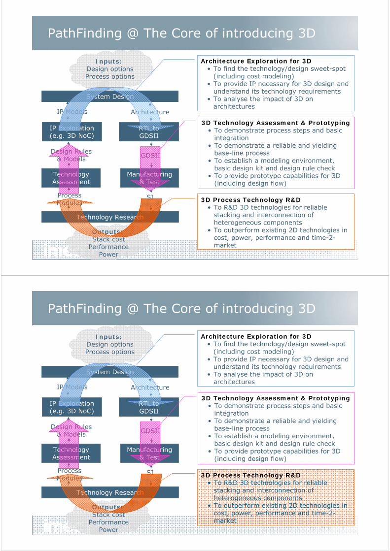
PathFinding @ The Core of introducing 3D
Design Rules & Models
TechnologyAssessment
IP Exploration(e.g. 3D NoC)
IP Models
GDSII
Technology Research
Process Modules
System Design
RTL toGDSII
Manufacturing& Test
Architecture
Inputs: Design optionsProcess options
SI
Architecture Exploration for 3D• To find the technology/design sweet-spot
(including cost modeling) • To provide IP necessary for 3D design and
understand its technology requirements• To analyse the impact of 3D on
architectures
3D Process Technology R&D• To R&D 3D technologies for reliable
stacking and interconnection of heterogeneous components
• To outperform existing 2D technologies in cost, power, performance and time-2-market
3D Technology Assessment & Prototyping• To demonstrate process steps and basic
integration• To demonstrate a reliable and yielding
base-line process• To establish a modeling environment,
basic design kit and design rule check • To provide prototype capabilities for 3D
(including design flow)
Outputs:Stack cost
PerformancePower
Rudy Lauwereins© imec 2008 4
PathFinding @ The Core of introducing 3D
Design Rules & Models
TechnologyAssessment
IP Exploration(e.g. 3D NoC)
IP Models
GDSII
Technology Research
Process Modules
System Design
RTL toGDSII
Manufacturing& Test
Architecture
Inputs: Design optionsProcess options
SI
Architecture Exploration for 3D• To find the technology/design sweet-spot
(including cost modeling) • To provide IP necessary for 3D design and
understand its technology requirements• To analyse the impact of 3D on
architectures
3D Process Technology R&D• To R&D 3D technologies for reliable
stacking and interconnection of heterogeneous components
• To outperform existing 2D technologies in cost, power, performance and time-2-market
3D Technology Assessment & Prototyping• To demonstrate process steps and basic
integration• To demonstrate a reliable and yielding
base-line process• To establish a modeling environment,
basic design kit and design rule check • To provide prototype capabilities for 3D
(including design flow)
Outputs:Stack cost
PerformancePower

Rudy Lauwereins© imec 2008 5
3D TSV Technology Roadmap
Via size
Via pitch
Wafer thickness
TechnologyProgramme
Interconnect Hierarchy Bondpad (0-level) Global
levelIntermediate level
Local interconnect
• Use of standard Si• Multi-source possible• Post-foundry process• D2D or D2W stacking• Mainly parallel process• Strongly Cost driven
• Cu nail process in foundry• Thinning/stacking post-
foundry process• D2W or W2W stacking• Key: D2W/W2W alignment
accuracy, speed and yield• Mainly parallel process
• Fully foundry level process• Requires use of SOI wafers• only W2W stacking possible• Extreme W2W alignment
accuracy required • Sequential process flow• Compound yield issues
80 um
100 um
50 um 1 um
10 um
5 um 2 um
4 um
100 nm
1 um 200 nm
Active layer only - SOI
500 nm25 um
40 um
50 um 15 um20 um
5 um
50 um 30 um
10 um
10 um
20 um
30 um
3D-WLP TSV 3D-SIC Cu-nails TSV 3D-IC Sub-μ TSV
IIAP 3D-WLP IIAP 3D-SIC
Rudy Lauwereins© imec 2008 6
3D Interconnect TechnologyDevelopments at IMEC
HR-SI rf-IPD wafer (100µm)
SiO2 layer
Metal 1(Al)
Polymerlayer
Electroplated Cu layer
IC1
IC3IC2
Cu nail
landing pad
BCB
3D-SIC Cu-nail TSV 3D-WLP Ultra-thin
Chip stackingCu/polymer TSV

Rudy Lauwereins© imec 2008 7
PathFinding @ The Core of introducing 3D
Design Rules & Models
TechnologyAssessment
IP Exploration(e.g. 3D NoC)
IP Models
GDSII
Technology Research
Process Modules
System Design
RTL toGDSII
Manufacturing& Test
Architecture
Inputs: Design optionsProcess options
SI
Architecture Exploration for 3D• To find the technology/design sweet-spot
(including cost modeling) • To provide IP necessary for 3D design and
understand its technology requirements• To analyse the impact of 3D on
architectures
3D Process Technology R&D• To R&D 3D technologies for reliable
stacking and interconnection of heterogeneous components
• To outperform existing 2D technologies in cost, power, performance and time-2-market
3D Technology Assessment & Prototyping• To demonstrate process steps and basic
integration• To demonstrate a reliable and yielding
base-line process• To establish a modeling environment,
basic design kit and design rule check • To provide prototype capabilities for 3D
(including design flow)
Outputs:Stack cost
PerformancePower
Rudy Lauwereins© imec 2008 8
Test Chip Design
• Test Structures for Design Rule Assessment– TSV characteristics: capacitance, resistance, yield, stack alignment, …
– Impact of TSV and of relative process on transistors
– Impact of TSV and of relative process on wires
– Diode-based thermometers, hot-spot heaters to be placed in different chip locations
– Structures for processing and for std tests
– RF test structures
– Dedicated test structures by our partners
– Small 3D circuits (e.g. ring oscillator with stages distributed in different chip level, …)
• For 200mm wafers (2 metal layers -130nm platform technology)
• TSV: Via diameter: 5um/Via pitch: 10um• D2W and W2W possibilities at the same
time
Rudy Lauwereins© imec 2008 9
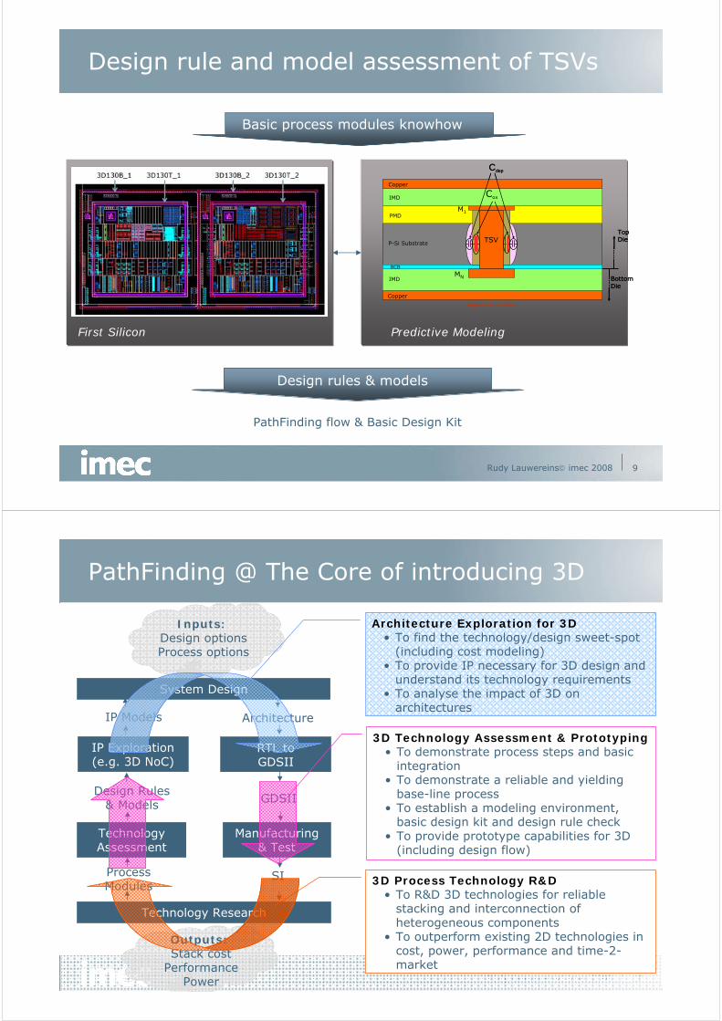
Design rule and model assessment of TSVs
Basic process modules knowhow
Design rules & models
First Silicon Predictive Modeling
BottomDie
TopDie
Diagram Not To Scale
BCB
PMDM1
MN
IMD
TSV
Cdep
Cox
P-Si Substrate
IMD
Copper
Copper
BottomDie
TopDie
Diagram Not To Scale
BCB
PMDM1
MN
IMD
TSV
Cdep
Cox
P-Si Substrate
IMD
Copper
Copper
PathFinding flow & Basic Design Kit
Rudy Lauwereins© imec 2008 10
PathFinding @ The Core of introducing 3D
Design Rules & Models
TechnologyAssessment
IP Exploration(e.g. 3D NoC)
IP Models
GDSII
Technology Research
Process Modules
System Design
RTL toGDSII
Manufacturing& Test
Architecture
Inputs: Design optionsProcess options
SI
Architecture Exploration for 3D• To find the technology/design sweet-spot
(including cost modeling) • To provide IP necessary for 3D design and
understand its technology requirements• To analyse the impact of 3D on
architectures
3D Process Technology R&D• To R&D 3D technologies for reliable
stacking and interconnection of heterogeneous components
• To outperform existing 2D technologies in cost, power, performance and time-2-market
3D Technology Assessment & Prototyping• To demonstrate process steps and basic
integration• To demonstrate a reliable and yielding
base-line process• To establish a modeling environment,
basic design kit and design rule check • To provide prototype capabilities for 3D
(including design flow)
Outputs:Stack cost
PerformancePower
Rudy Lauwereins© imec 2008 11
Path finding - a first illustration
IMEC’s SDR next generation
3D Integration Scenarios
Performance Analysis for Various Technology ParametersPreliminary cost analysis
4.1
4.2
4.3
4.4
4.5
4.6
4.7
4.8
0 0.02 0.04 0.06 0.08 0.1 0.12 0.14 0.16 0.18 0.2
TSV capacitance (pF)
Crit
ical
pat
h de
lay
(ns)
Baseline 2D design
3D on 2D area
3D on 1/2 2D area
Rudy Lauwereins© imec 2008 12
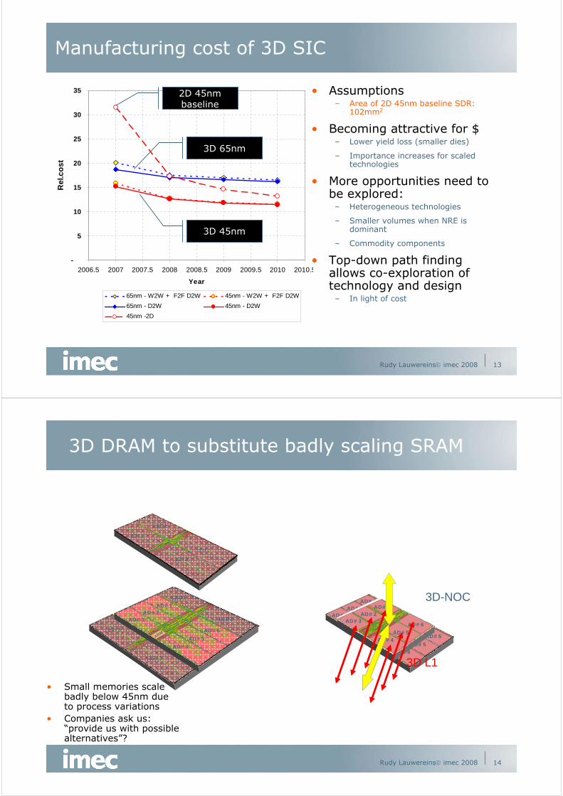
Manufacturing cost of 3D SIC
• Assumptions– Area of 2D 45nm baseline SDR:
34mm2
– 3D technology: TSV 10µm
– Homogeneous technology layers, custom fabricated
– Manufacturing cost is dominant
• Conclusions– 3D using older (65nm)
technology is never attractivecompared to 2D 45nm baseline
– 3D using 45nm technology is only attractive on the short term
• But ...
3.0
3.5
4.0
4.5
5.0
5.5
6.0
2006.5 2007 2007.5 2008 2008.5 2009 2009.5 2010 2010.5
Year
Rel
.co
st
65nm - W2W + F2F D2W 45nm - W2W + F2F D2W
65nm - D2W 45nm - D2W
45nm -2D
3D 65nm scenario 1
3D 65nm scenario 2
2D 45 nmbaseline
3D 45nm scenario 1 & 2
Rudy Lauwereins© imec 2008 13
Manufacturing cost of 3D SIC
• Assumptions– Area of 2D 45nm baseline SDR:
102mm2
• Becoming attractive for $– Lower yield loss (smaller dies)
– Importance increases for scaled technologies
• More opportunities need to be explored:
– Heterogeneous technologies
– Smaller volumes when NRE is dominant
– Commodity components
• Top-down path finding allows co-exploration of technology and design
– In light of cost
-
5
10
15
20
25
30
35
2006.5 2007 2007.5 2008 2008.5 2009 2009.5 2010 2010.5
Year
Re
l.co
st
65nm - W2W + F2F D2W 45nm - W2W + F2F D2W
65nm - D2W 45nm - D2W
45nm -2D
2D 45nmbaseline
3D 65nm
3D 45nm
Rudy Lauwereins© imec 2008 14
L2D1
L2D2
L2I2
L2I1
AD#1AD#2
AD#3
AD#6
AD#5AD#4
ARM
L2D1
L2D2
L2I2
L2I1
L2D1
L2D2
L2I2
L2I1
ARM
AD#1AD#2
AD#3
AD#6
AD#5AD#4
ARM
AD#1AD#2
AD#3
AD#6
AD#5AD#4
AD#1AD#2
AD#3
L1#6
L1#5
L1#4
L1#1L1#2
L1#3
AD#6
AD#5AD#4
L1#1L1#2
L1#3 L1#6
L1#5
L1#4
AD#1AD#2
AD#3AD#6
AD#5AD#4
3D-NOC
3D L1
3D DRAM to substitute badly scaling SRAM
• Small memories scale badly below 45nm due to process variations
• Companies ask us: “provide us with possible alternatives”?

Rudy Lauwereins© imec 2008 15© imec 2007
3D DRAM as replacement for embedded SRAM -Preliminary results
Paul Marchal© imec restricted 2007 1515
• DRAM cells are 10x smaller compared to SRAM • More than 2x area reduction by just changing the cell on a SRAM matrix• Further reduction is possible, by optimizing the peripherals
• Similar read/write power for same performance• Less power to retain data ( 496 54 pW/bits), because refresh power is less compared to SRAM cell leakage• TSV power cost can be contained
128 Kbits
0
2
4
6
8
10
0 0.1 0.5Activity @ f= 500MHz
PS
RA
M /
PD
RA
M
128kB memory@500Mhz
More savings for infrequently
used memories (e.g., L2s)
Rudy Lauwereins© imec 2008 16
3D: Partnering for Cost Effective Research
MemoryIDM
3D Program
LogicIDM
STMicroelectronicsSTMicroelectronics
Foundries
Equipment& MaterialsSuppliers
LamRESEARCH
SAT
EDA
Fabless

Rudy Lauwereins© imec 2008 17


![SMOKE: Single-Stage Monocular 3D Object Detection via ... · SMOKE: Single-Stage Monocular 3D Object Detection via Keypoint Estimation ... The early work 3DOP [4] generates 3D proposals](https://static.fdocuments.in/doc/165x107/5f06f7957e708231d41aa186/smoke-single-stage-monocular-3d-object-detection-via-smoke-single-stage-monocular.jpg)