Latches and flip flops
26
Latches and Flip- Flops GOVT. Municipal Degree College FSD… CSI-403 Digital logic and computer design… Presentation topic.
-
Upload
mubashir-farooq -
Category
Design
-
view
1.643 -
download
0
Transcript of Latches and flip flops

Latches and Flip-Flops
GOVT. Municipal Degree College FSD…
CSI-403 Digital logic and computer design…
Presentation topic.
Latches and Flip-Flops…
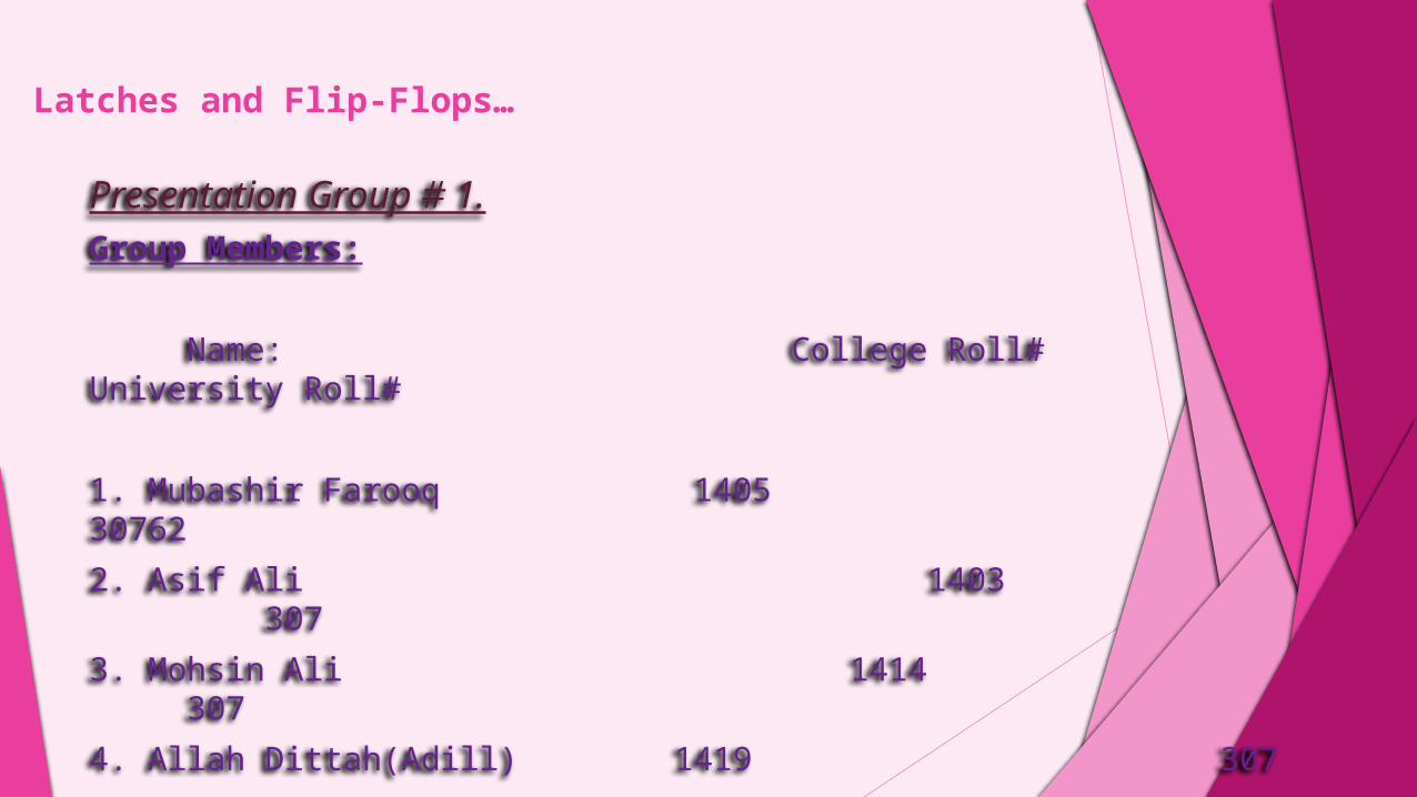
Presentation Group # 1.Group Members:
Name: College Roll# University Roll#
1. Mubashir Farooq 1405 307622. Asif Ali 1403 3073. Mohsin Ali 1414 3074. Allah Dittah(Adill) 1419 307

Table of contents: In this lecture we will discuses these topics
what are latches and flip plop. what is different between both. Different types of flip flop. Different types of latches. Explanation of all types of latches with
diagrams. Explanation of all types of flip flop with
diagrams.
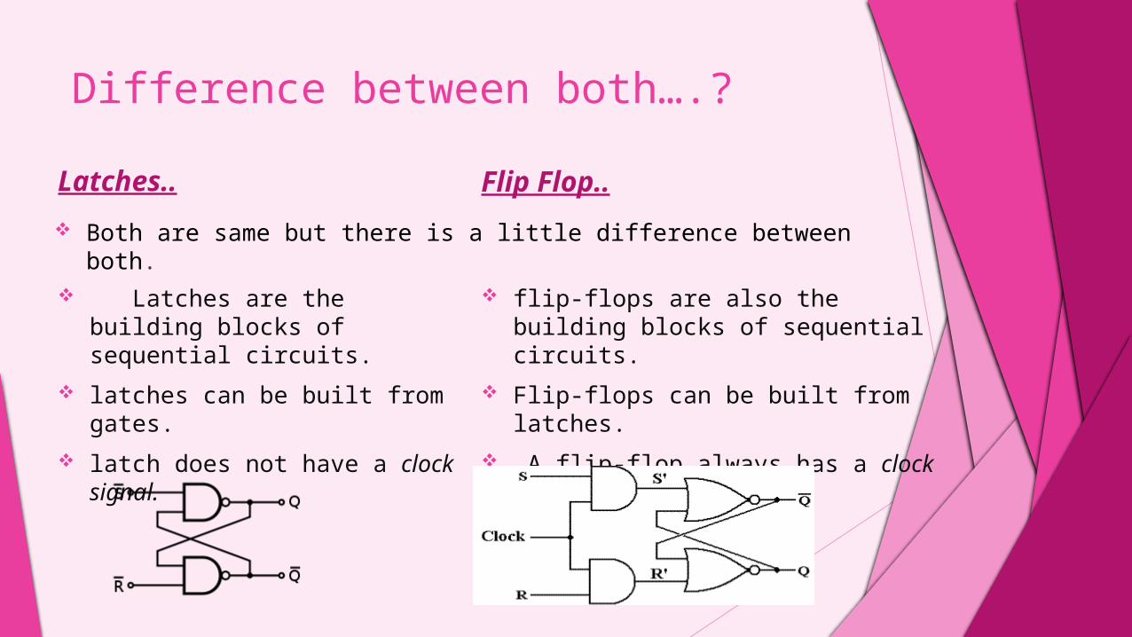
Difference between both….? Latches..
Latches are the building blocks of sequential circuits.
latches can be built from gates.
latch does not have a clock signal.
Flip Flop..
flip-flops are also the building blocks of sequential circuits.
Flip-flops can be built from latches. A flip-flop always has a clock
Signal
Both are same but there is a little difference between both.
What are flip flops. In electronics, a flip-flop or latch is a circuit that has two stable states and can be used to store state information. A flip-flop is a bistable multivibrator. The circuit can be made to change state by signals applied to one or more control inputs and will have one or two outputs. It is the basic storage element in sequential logic.
Flip-flops maintain their state indefinitely until an input pulse called a trigger is received. When a trigger is received, the flip-flop outputs change state according to defined rules and remain in those states until another trigger is received.

Uses of flip flops. Flip flop and latches are the circuits that can store and
remember information. They're the kind of circuits that are used in computers to store program information like RAM memory and Registers.
Flip-flops can be used to store one bit, or binary digit, of data. The data may represent the state of a sequencer, the value of a counter, an ASCII character in a computer's memory or any other piece of information.

Types Of flip flop..
Some various types of flip-flop circuits are as follows:
RS flip-flop circuit Clocked RS flip flop circuit D flip flop circuit Jk flip flop circuit T flip flop circuit

1. RS flip flop. DEFINITION: “A circuit containing cross coupled connection, which is used to remain a memory state stable by using asynchronous sequential circuits, is called direct-coupled or RS flip flop.” EXPLANATION: Each flip flop has two inputs and two outputs. The inputs are denoted by R and S and outputs are denoted by Q and Q’. These circuits can be implemented through “NOR” and “NAND” gate

Implementation:These circuits are implemented through NOR and NAND gates.
Logic Diagram:
Truth Table: S R Q Q’ 0 0 1 1 Not Allowed
1 0 0 1 Reset
0 1 1 0 Set
1 1 Q Q’ Memory state
Q
Q'
S'
R'
( a )
Note: By using the sign of invert we can change it into NOR’s table.

How the above circuit works:Memory State:In above circuit when two inputs are given as S=0 and R=0 then the memory remains stable.Re-set state:When inputs are given as S=0 and R=1, then the output comes Q=0 AND Q’=1.(“WHEN Q’ comes 1 this state is called RE-SET state”)Set state:When inputs are given as S=1 and R=0, then the output comes Q=1 AND Q’=0.(“WHEN Q comes 1 this state is called SET state”)Not Allowed state:When the outputs come against the inputs then this state is called not allowed.

2. Clocked SR Circuit: DEFINITION:“A circuit which is used to remain a memory stable by using “clock signals” is called clocked SR circuit.”Clock Signal:“Is used to perform any process in a circuit is called Clock signal.”Basically clock signals are electrical pluses which are in the form of 1 or 0.Note : A process is performed only when it is in the form of “1”EXPLANATION OF Clocked SR Circuit: Memory State:In above circuit when two inputs are given as CLK=0, S=0 and R=0 then the memory remains stable.

Re-set state:When inputs are given as clk=1,S=0 and R=1, then the output comes Q=0 AND Q’=1.(“WHEN Q’ comes 1 this state is called RE-SET state”)Set state:When inputs are given as cl1=1,S=1 and R=0, then the output comes Q=1 AND Q’=0.(“WHEN Q comes 1 this state is called SET state”)Not Allowed state:When the outputs come against the inputs then this state is called not allowed.
Clocked SR Circuit:
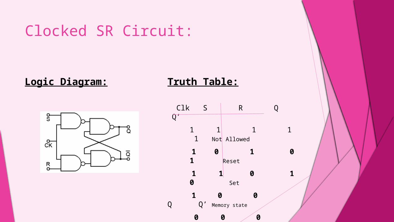
Logic Diagram: Truth Table: Clk S R Q Q’ 1 1 1 1 1 Not Allowed
1 0 1 0 1 Reset
1 1 0 1 0 Set
1 0 0 Q Q’ Memory state
0 0 0 1 0 Memory state
Clocked SR Circuit:

3. D Flip-Flop: DEFINITION: A circuit which is used to remove Clocked SR Circuit’s “not allowed state” more circuit’s stability is called D flip flop.A circuit using Inverter is basically a SR circuit, which reduces the no. of inputs from two to one . It also called D-Latch. EXPLANATION:It is basically modification of SR clocked circuit by using 5 gates . NAND gates 1 and 2 form a basic Flip-flop and gates 3 and 4 modify it into a clocked RS flip-flop. Its working is given below by using circuits………… Uses of D Flip-Flop:The D Flip-Flop receives the designation from its ability to transfer” data” into a flip-flop.
Explanation through circuit :This circuit is being constructed by using “Inverter with R” .Memory state:When Cp=0 and D=don’t care condition then memory stays stable.Re-set state:When inputs are given as Cp=1,D=0, then the output comes Q=0 AND Q’=1.(“WHEN Q’ comes 1 this state is called RE-SET state”)Set state:When inputs are given as Cp=1,D=1, then the output comes Q=1 AND Q’=0.(“WHEN Q comes 1 this state is called SET state”)
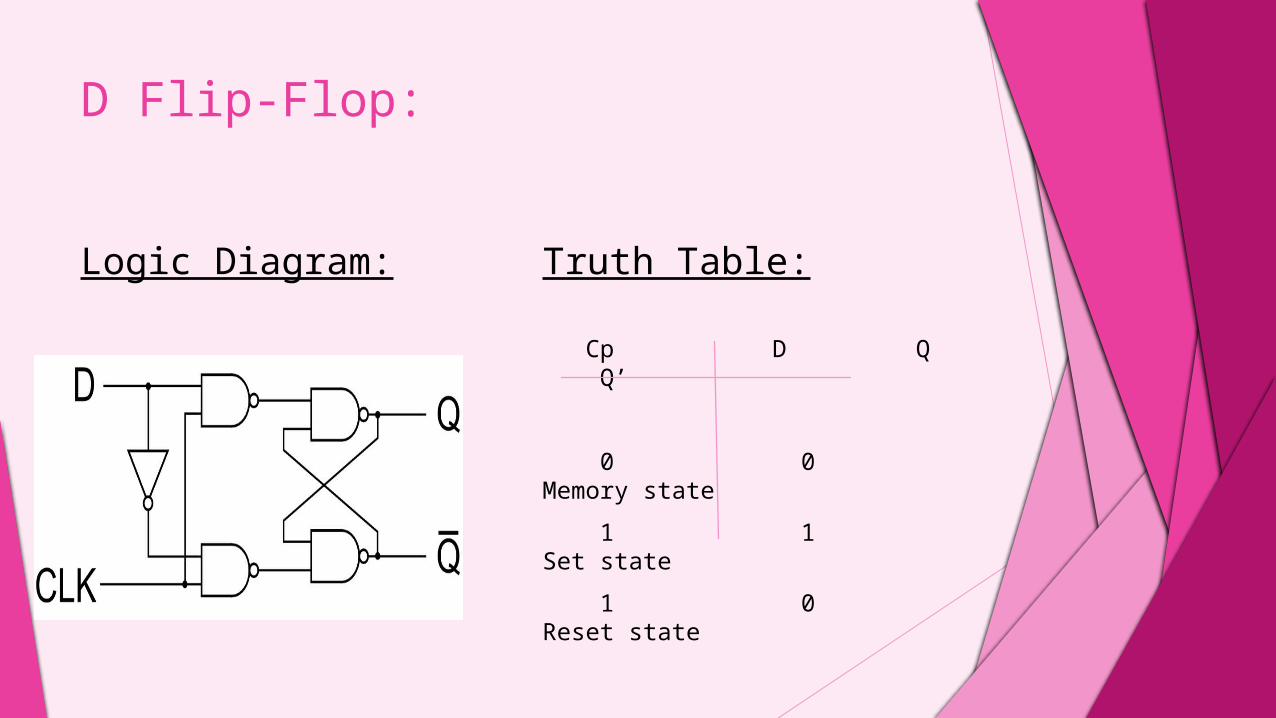
Logic Diagram: Truth Table: Cp D Q Q’
0 0 Memory state 1 1 Set state 1 0 Reset state
D Flip-Flop:

4. JK Flip-Flop: Definition:“A JK flip-flop is a refinement of RS flip-flop circuit in that the determinate state of RS type is defined in the JK type. Means J and K behave like S and R to set and clear the flip-flop.”
Note: The letter j is used for set and the letter K is used for Reset.
Note: It is also used for removing not allowed state for memory state.A clocked JK flip-flop circuit is shown in the bellow diagram.Working Of JK flip-flop:It is used to give following states when we give suitable inputs.

Memory state:When Clk=0 and J and K=don’t care conditions then memory stays stable.ALSO:When Clk=1 and both J and K are 0,then memory also stays stable.Set state:When inputs are given as Clk=1 and J=1 and K=0, then the output comes Q=1 AND Q’=0.(“WHEN Q comes 1 this state is called SET state”)ReSet state:When inputs are given as Clk=1 and J=0 and K=1, then the output comes Q=0 and Q’=1.(“WHEN Q’ comes 1 this state is called RESET state”)
JK Flip-Flop:

Circuit Diagram: Truth Table: Clk J K Q Q’
1 0 0 Memory state 0 0 1 Memory state 1 1 0 Set state 1 0 1 Reset state
JK Flip-Flop:

5. T-Flip Flops The T or "toggle" flip-flop changes its output on each clock edge, giving an output which is half the frequency of the signal to the T input. It is useful for constructing binary counters, frequency dividers, and general binary addition devices. It can be made from a J-K flip-flop.The T flip-flop can be constructed using a D flip-flop with the two outputs Q and Q' feedback to the D input through a multiplexer that is controlled by the T input as shown in Figure
Circuit Diagram:

What are latches. A latch is an example of a bistable multivibrator that is, a device with exactly two stable states. These states are high-output and low-output. A latch has a feedback path, so information can be retained by the device. Therefore latches can be memory devices, and can store one bit of data for as long as the device is powered. As the name suggests, latches are used to "latch onto" information and hold in place. Latches are very similar to flip-flops, but are not synchronous devices, and do not operate on clock edges as flip-flops do.
Some various types of flip-flop circuits are as follows: SR latch Gated SR latch D latch

SR Latches. An SR latch (Set/Reset) is an asynchronous device: it works independently of control signals and relies only on the state of the S and R inputs. In the image we can see that an SR latch can be created with two NOR gates that have a cross-feedback loop. SR latches can also be made from NAND gates, but the inputs are swapped and negated. In this case, it is sometimes called an SR latch.
Circuit Diagram:

Gated SR latch. The gated SR latch is a simple extension of the SR latch which provides an Enable line which must be driven high before data can be latched. Even though a control line is now required, the SR latch is not synchronous, because the inputs can change the output even in the middle of an enable pulse.
Circuit Diagram.

D Latch. The D latch (D for "data") or transparent latch is a simple extension of the
gated SR latch that removes the possibility of invalid input states.
Since the gated SR latch allows us to latch the output without using the S or R inputs, we can remove one of the inputs by driving both the Set and Reset inputs with a complementary driver: we remove one input and automatically make it the inverse of the remaining input.
Circuit Diagram:

For attention…