Last Lecture - University of California, San Diego · Full Adder 7 You can use 2 half ... –...
47
Last Lecture 1 • The basic component of a digital circuit is the MOS transistor • Transistor have instrinsic resistance and capacitance, so voltage values in the circuit take some time to change (“delay”) • There exist two kinds: nMOS and pMOS, with complementary behavior and advantages/disadvantages • A logic gate implementing a certain boolean function can be built with a circuit composed of: • A Pull-Down network of nMOS • A Pull-Up network of pMOS • There exist automatic rules to determine the topology of the Pull- Down and the Pull-Up network for a gate • Multiple gates can be connected together to form more complicated components • Yesterday in CSE140 we saw logic gates (like NOT and NAND) • Today here we will look at slightly more high level components (because it’s what you have to implement in homework 2)
Transcript of Last Lecture - University of California, San Diego · Full Adder 7 You can use 2 half ... –...

Last Lecture
1
• The basic component of a digital circuit is the MOS transistor
• Transistor have instrinsic resistance and capacitance, so voltage
values in the circuit take some time to change (“delay”)
• There exist two kinds: nMOS and pMOS, with complementary
behavior and advantages/disadvantages
• A logic gate implementing a certain boolean function can be built with
a circuit composed of:
• A Pull-Down network of nMOS
• A Pull-Up network of pMOS
• There exist automatic rules to determine the topology of the Pull-
Down and the Pull-Up network for a gate
• Multiple gates can be connected together to form more complicated
components
• Yesterday in CSE140 we saw logic gates (like NOT and NAND)
• Today here we will look at slightly more high level components
(because it’s what you have to implement in homework 2)

This Lecture
2
• Some components (useful for the homework)
• Verilog HDL (will continue next lecture)

3
CSE140L: Components and Design
Techniques for Digital Systems Lab
Some basic digital components

Half Adder
4
A,B : Inputs
S: Sum
C: Carry
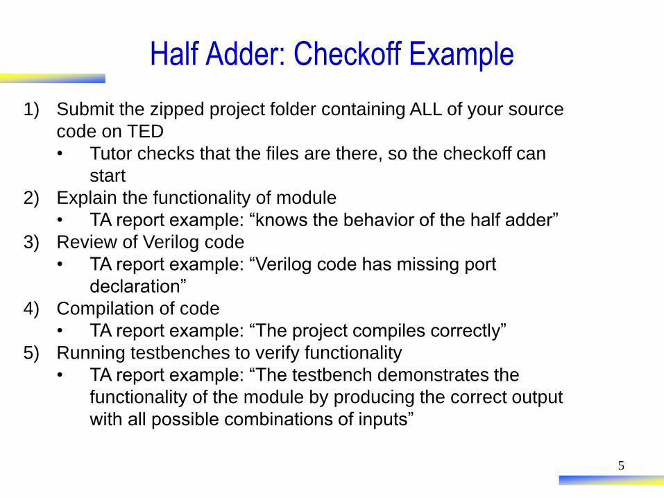
Half Adder: Checkoff Example
5
1) Submit the zipped project folder containing ALL of your source
code on TED
• Tutor checks that the files are there, so the checkoff can
start
2) Explain the functionality of module
• TA report example: “knows the behavior of the half adder”
3) Review of Verilog code
• TA report example: “Verilog code has missing port
declaration”
4) Compilation of code
• TA report example: “The project compiles correctly”
5) Running testbenches to verify functionality
• TA report example: “The testbench demonstrates the
functionality of the module by producing the correct output
with all possible combinations of inputs”
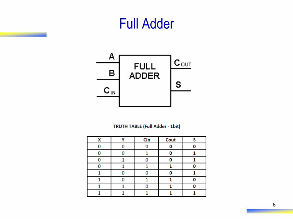
Full Adder
6

Full Adder
7
You can use 2 half adders and a OR gate to implement the Full Adder
8
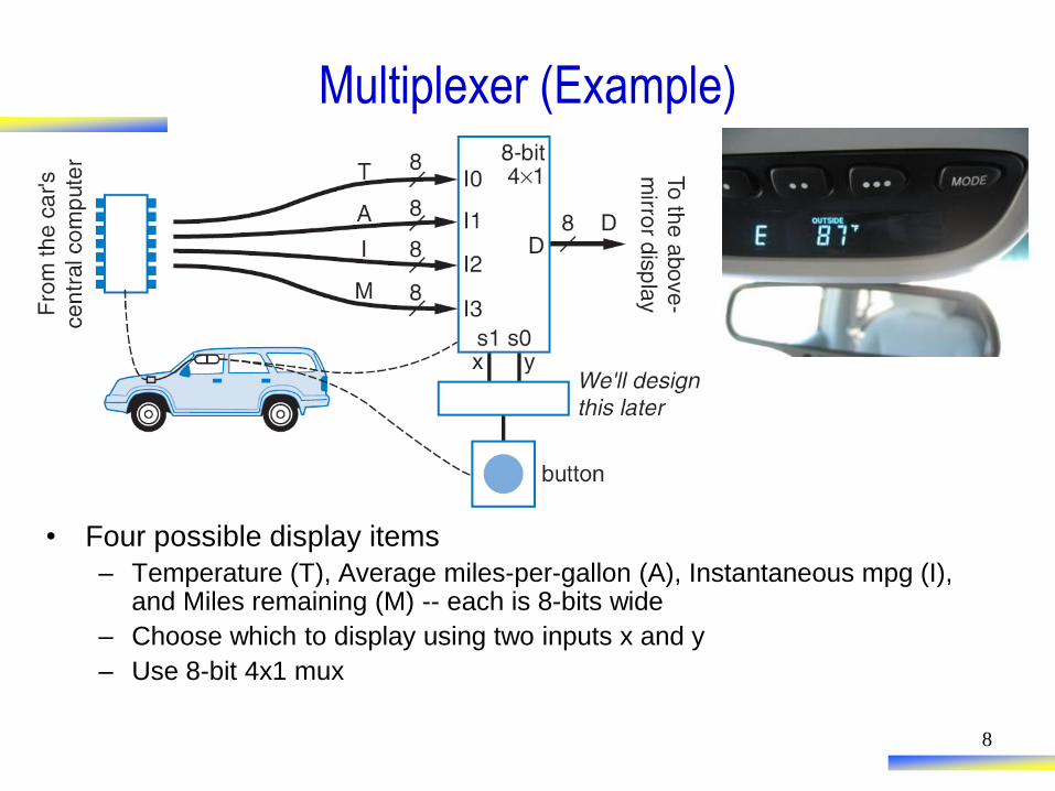
Multiplexer (Example)
• Four possible display items
– Temperature (T), Average miles-per-gallon (A), Instantaneous mpg (I), and Miles remaining (M) -- each is 8-bits wide
– Choose which to display using two inputs x and y
– Use 8-bit 4x1 mux

9
I0I1I2I3I4I5I6I7
A B C
8:1mux
Z
I0I1I2I3
A B
4:1mux
ZI0I1
A
2:1mux
Z
Multiplexers/selectors
• 2:1 mux: Z = A'I0 + AI1
• 4:1 mux: Z = A'B'I0 + A'BI1 + AB'I2 + ABI3
• 8:1 mux: Z = A'B'C'I0 + A'B'CI1 + A'BC'I2 + A'BCI3 +
AB'C'I4 + AB'CI5 + ABC'I6 + ABCI7
• In general: σ𝑘=02𝑛−1𝑚𝑘𝐼𝑘
– shorthand form for a 2n:1 Mux
10For example
10
11
0

10
Demultiplexers/decoders
• Decoders/demultiplexers: general concept
– single data input, n control inputs, 2n outputs
– control inputs (called “selects” (S)) represent binary index of
output to which the input is connected
– data input usually called “enable”
1
1 0
00
01
For example

11
CSE140L: Components and Design
Techniques for Digital Systems Lab
Verilog HDL
Slides from Tajana Simunic Rosing
Source: Eric Crabill, Xilinx

Hardware description languages
• Used to describe & model the operation of digital circuits.
• Specify simulation procedure for the circuit and check its
response.
– Simulation requires a logic simulator.
• Synthesis: transformation of the HDL description into a
physical implementation (transistors, gates)
– When a human does this, it is called logic design.
– When a machine does this, it is called synthesis.

HDLs
• Abel (circa 1983) - developed by Data-I/O
– targeted to programmable logic devices
– not good for much more than state machines
• ISP (circa 1977) - research project at CMU
– simulation, but no synthesis
• Verilog (circa 1985) - developed by Gateway (absorbed by Cadence)
– similar to C
– delays are the only interaction with the simulator
– fairly efficient and easy to write
– IEEE standard
• VHDL (circa 1987) - DoD sponsored standard
– VHSIC Hardware Description Language
(VHSIC is Very High Speed Integrated Circuit).
– simulation semantics visible; very general but verbose
– IEEE standard
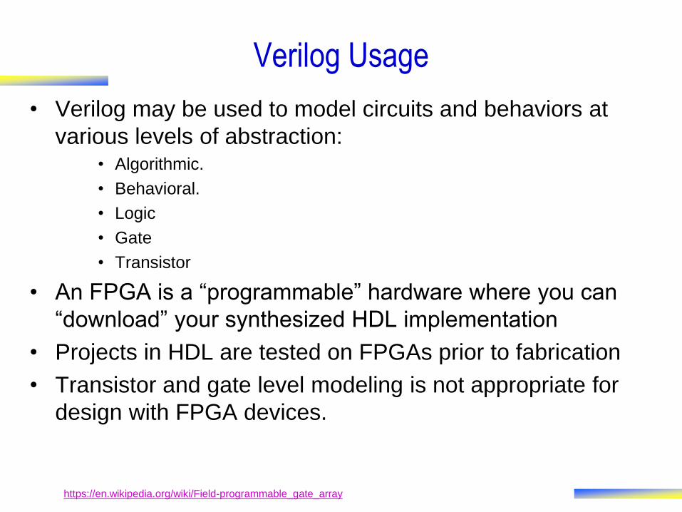
Verilog Usage
• Verilog may be used to model circuits and behaviors at
various levels of abstraction:• Algorithmic.
• Behavioral.
• Logic
• Gate
• Transistor
• An FPGA is a “programmable” hardware where you can
“download” your synthesized HDL implementation
• Projects in HDL are tested on FPGAs prior to fabrication
• Transistor and gate level modeling is not appropriate for
design with FPGA devices.
https://en.wikipedia.org/wiki/Field-programmable_gate_array

Verilog
• Supports structural and behavioral descriptions
• Structural
– explicit structure of the circuit
– e.g., each logic gate instantiated and connected to others
• Behavioral
– program describes input/output behavior of circuit
– many structural implementations could have same behavior
– e.g., different implementation of one Boolean function

module xor_gate (out, a, b);
input a, b;
output out;
wire abar, bbar, t1, t2;
inverter invA (abar, a);
inverter invB (bbar, b);
and_gate and1 (t1, a, bbar);
and_gate and2 (t2, b, abar);
or_gate or1 (out, t1, t2);
endmodule
Structural model
invA
invB and1
and2
or1a
b
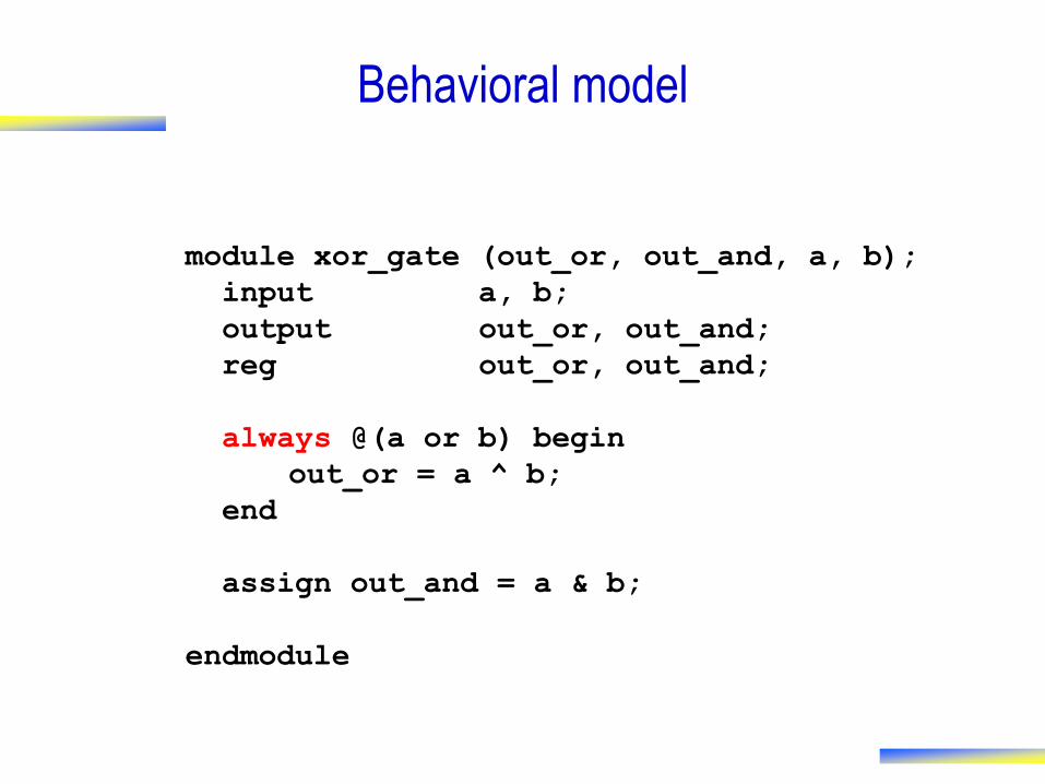
module xor_gate (out_or, out_and, a, b);
input a, b;
output out_or, out_and;
reg out_or, out_and;
always @(a or b) begin
out_or = a ^ b;
end
assign out_and = a & b;
endmodule
Behavioral model

Data Values
• For our logic design purposes, we’ll consider Verilog to
have four different bit values:
– 0, logic zero.
– 1, logic one.
– z, high impedance.
– x, unknown.

Data Types and Values
• There are two main data types in Verilog.
– Wires.
– Regs.
• These data types may be single bit or multi-bit.
– The general syntax is: {bit width}’{base}{value}
• 4’d14 // 4-bit value, specified in decimal
• 4’he // 4-bit value, specified in hex
• 4’b1110 // 4-bit value, specified in binary
• 4’b10xz // 4-bit value, with x and z, in binary

Data Types
• Wires:
– “continuously assigned” values and do not store information.
– may have multiple drivers assigning values.
– When multiple drivers exist, the simulator resolves them into a
single value for the wire.
– Every time a driver changes its output value, the resulting wire
value is re-evaluated.
• This behaves much like an electrical wire...

Data Types
• Regs
– “procedurally assigned” values that store information until the next
value assignment is made.
– can be used to model combinational or sequential logic.
– The name “reg” does not mean it is a register!
– A reg may be assigned by multiple processes.
– Other reg varieties include integer, real, and time.

Lecture 3
22

Checkoff
• Before Wednesday at 4.30pm (last available office hour)
– Meet with instructor/TA/tutor during office hours
– Submit source code on TED
– For HW2:
• For 2 modules (picked randomly): quick review of the code
• You’ll be asked to run the testbenches for 2 modules and explain how they
work.
23

Modules and Ports
• Consider a top level module declaration:module testbench;
// Top level modules do not have ports.
endmodule
• Consider a module declaration with ports:module two_input_xor (in1, in2, out);
input in1, in2;
output out;
// We’ll add more later…
endmodule
Module
Ports: define how
the module
interacts with the
external world

Modules and Ports
• Ports may be of type {input, output, inout}and can also be multiple bits wide.
module some_random_design (fred, bob, joe, sam, tom, ky);
input fred; // 1-bit input port
input [7:0] bob; // 8-bit input port
output joe; // 1-bit output port
output [1:0] sam; // 2-bit output port
inout tom; // 1-bit bidirectional port
inout [3:0] ky; // 4-bit bidirectional port
// Some design description would be here…
endmodule

Port and Data Types
• Input port:
– driven from outside the module by a wire or a reg,
– inside the module it can only drive a wire
• Output port
– driven from inside the module by a wire or a reg,
– outside the module it can only drive a wire.
• Inout port
– May be driven by a wire, and drive a wire.
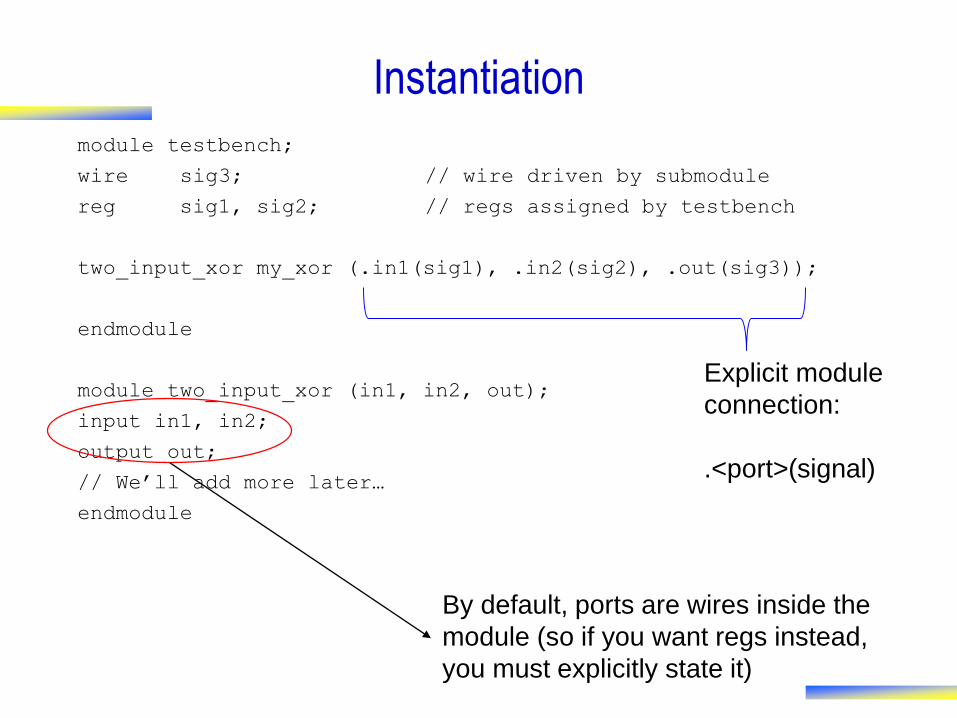
Instantiation
module testbench;
wire sig3; // wire driven by submodule
reg sig1, sig2; // regs assigned by testbench
two_input_xor my_xor (.in1(sig1), .in2(sig2), .out(sig3));
endmodule
module two_input_xor (in1, in2, out);
input in1, in2;
output out;
// We’ll add more later…
endmodule
Explicit module
connection:
.<port>(signal)
By default, ports are wires inside the
module (so if you want regs instead,
you must explicitly state it)
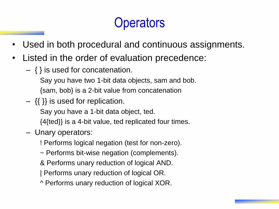
Operators
• Used in both procedural and continuous assignments.
• Listed in the order of evaluation precedence:
– { } is used for concatenation.
Say you have two 1-bit data objects, sam and bob.
{sam, bob} is a 2-bit value from concatenation
– {{ }} is used for replication.
Say you have a 1-bit data object, ted.
{4{ted}} is a 4-bit value, ted replicated four times.
– Unary operators:
! Performs logical negation (test for non-zero).
~ Performs bit-wise negation (complements).
& Performs unary reduction of logical AND.
| Performs unary reduction of logical OR.
^ Performs unary reduction of logical XOR.

Operators cont.
• Arithmetic operators (signed and can generate carry out):* Multiplication.
/ Division.
% Modulus.
+ Addition.
- Subtraction.
• Logical shift operators:<< Shift left.
>> Shift right.
• Relational operators:> Greater than.
< Less than.
>= Greater than or equal.
<= Less than or equal.
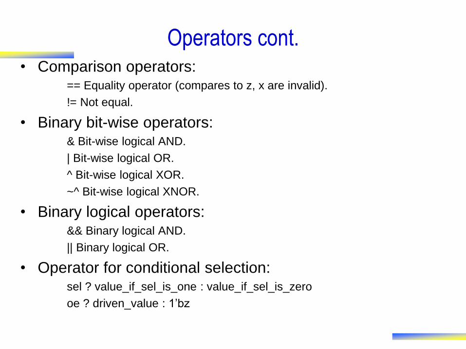
Operators cont.• Comparison operators:
== Equality operator (compares to z, x are invalid).
!= Not equal.
• Binary bit-wise operators:& Bit-wise logical AND.
| Bit-wise logical OR.
^ Bit-wise logical XOR.
~^ Bit-wise logical XNOR.
• Binary logical operators:&& Binary logical AND.
|| Binary logical OR.
• Operator for conditional selection:sel ? value_if_sel_is_one : value_if_sel_is_zero
oe ? driven_value : 1’bz

Continuous Assignment
• Continuous assignments are made with the assign
statement:
– assign LHS = RHS;
• The left hand side, LHS, must be a wire.
• The right hand side, RHS, may be a wire, a reg, a constant, or
expressions with operators using one or more wires, regs, and
constants.
• The value of the RHS is continuously driven onto the wire
of the LHS.
• Values x and z are allowed and processed.
• All assign statements operate concurrently.

Continuous Assignment
module two_input_xor (in1, in2, out);
input in1, in2; // use these as a wire
output out; // use this as a wire
assign out = in1 ^ in2;
endmodule
module two_input_xor (in1, in2, out);
input in1, in2;
output out;
wire product1, product2;
assign product1 = in1 & !in2; // could have done all in
assign product2 = !in1 & in2; // assignment of out with
assign out = product1 | product2; // bigger expression
endmodule

Continuous Assignment
module two_input_xor (in1, in2, out);
input in1, in2;
output out;
assign out = (in1 != in2);
endmodule
module two_input_xor (in1, in2, out);
input in1, in2;
output out;
assign out = in1 ? (!in2) : (in2);
endmodule
What does this line
represent?

Procedural Assignment
• Models combinational and sequential logic
• Operates concurrently and is preceded by event control.
• In block statements start with “begin” and end with “end”.
– Single assignments can omit begin and end.
• A sensitivity list specifies events which cause the
execution to begin:
– always @(a or b) // any changes in a or b
– always @(posedge a) // a transitions from 0 to 1
– always @(negedge a) // a transitions from 1 to 0
– always @(a or b or negedge c or posedge d)

Procedural Assignment
initial
begin
// These procedural assignments are executed
// one time at the beginning of the simulation.
end
always @(sensitivity list)
begin
// These procedural assignments are executed
// whenever the events in the sensitivity list
// occur.
end
Procedural Assignment
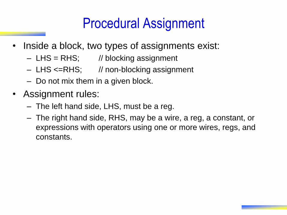
• Inside a block, two types of assignments exist:
– LHS = RHS; // blocking assignment
– LHS <=RHS; // non-blocking assignment
– Do not mix them in a given block.
• Assignment rules:
– The left hand side, LHS, must be a reg.
– The right hand side, RHS, may be a wire, a reg, a constant, or
expressions with operators using one or more wires, regs, and
constants.

Procedural Assignment
• Do I use blocking or non-blocking assignments?
– Blocking assignments are especially useful when describing
combinational logic.
• You can “build up” complex logic expressions.
• Blocking assignments make your description evaluate in the order
you described it.
– Non-blocking assignments are useful when describing sequential
logic.
• At a clock or reset event, all memory elements change state at the
same time, best modeled by non-blocking assignments.
• For conditional assignments use if-else and various types
of case statements.
• You also can make use of additional timing control:
– wait, #delay, repeat, while, etc…
Procedural Assignment
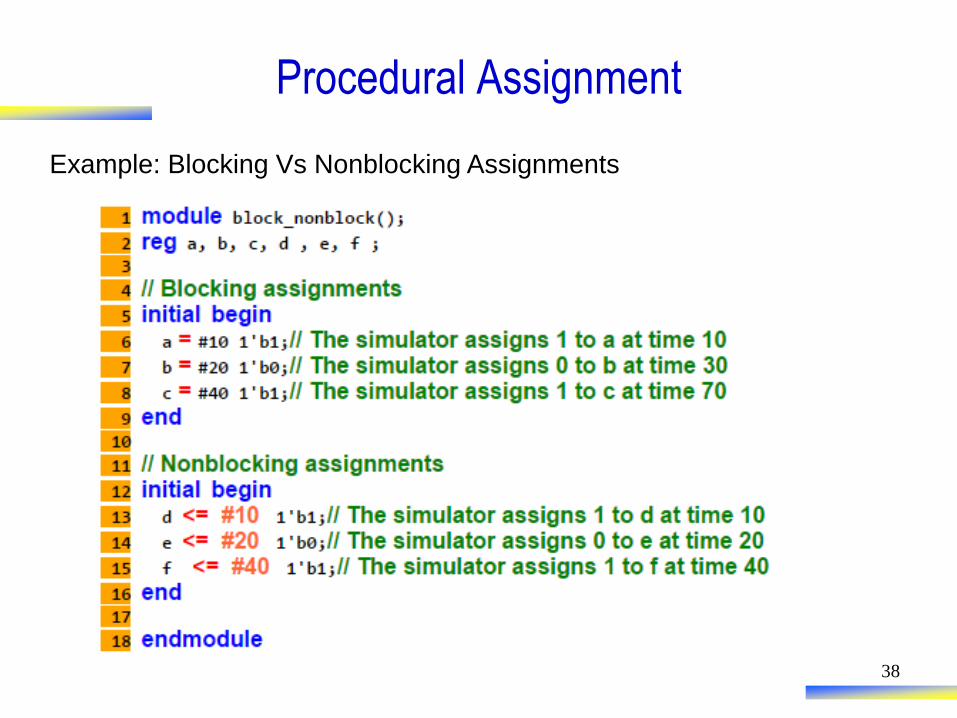
38
Example: Blocking Vs Nonblocking Assignments

Procedural Assignment
• Combinational logic using operators:module two_input_xor (in1, in2, out);
input in1, in2; // use these as wires
output out; // use this as a wire
reg out;
always @(in1 or in2) // Note that all input terms
begin // are in sensitivity list!
out = in1 ^ in2; // Or equivalent expression...
end
// I could have simply used:
// always @(in1 or in2) out = in1 ^ in2;
endmodule

Procedural Assignment
• Combinational logic using if-else:module two_input_xor (in1, in2, out);
input in1, in2; // use these as wires
output out; // use this as a wire
reg out;
always @(in1 or in2) // Note that all input terms
begin // are in sensitivity list!
if (in1 == in2) out = 1’b0;
else out = 1’b1;
end
endmodule

Procedural Assignment
• Combinational logic using case:module two_input_xor (in1, in2, out);
input in1, in2; // use these as wires
output out; // use this as a wire
reg out;
always @(in1 or in2) // Note that all input terms
begin // are in sensitivity list!
case ({in2, in1}) // Concatenated 2-bit selector
2’b01: out = 1’b1;
2’b10: out = 1’b1;
default: out = 1’b0;
endcase
end
endmodule

Delay Control
• You can add delay to continuous assignments.
– assign #delay LHS = RHS;
• The #delay indicates a time delay in simulation time units; for
example, #5 is a delay of five.
• This can be used to model physical delays of combinational logic.
• The simulation time unit can be changed by the Verilog
“ `timescale ” directive.
• Syntax:
– `timescale <reference_time_unit> / <precision>

Delay Control
• Control the timing of assignments in procedural blocks by:
– Level triggered timing control.
• wait (!reset);
• wait (!reset) a = b;
– Simple delays.
• #10;
• #10 a = b;
– Edge triggered timing control.
• @(a or b);
• @(a or b) c = d;
• @(posedge clk);
• @(negedge clk) a = b;

Delay Control
• Generation of clock and resets in testbench:reg rst, clk;
initial // this happens once at time zero
begin
rst = 1’b1; // starts off as asserted at time zero
#100; // wait for 100 time units
rst = 1’b0; // deassert the rst signal
end
always // this repeats forever
begin
clk = 1’b1; // starts off as high at time zero
#25; // wait for half period
clk = 1’b0; // clock goes low
#25; // wait for half period
end

System Tasks
• The $ sign denotes Verilog system tasks, there
are a large number of these, most useful being:
– $display(“The value of a is %b”, a);
• Used in procedural blocks for text output.
• The %b is the value format (binary, in this case…)
– $monitor
• Similar to display, but executes every time one of its parameter
changes
– $finish;
• Used to finish the simulation.
• Use when your stimulus and response testing is done.
– $stop;
• Similar to $finish, but doesn’t exit simulation.

module testbench (x, y);
output x, y;
reg [1:0] cnt;
initial begin
cnt = 0;
repeat (4) begin
#10 cnt = cnt + 1;
$display ("@ time=%d, x=%b, y=%b, cnt=%b",
$time, x, y, cnt); end
#10 $finish;
end
assign x = cnt[1];
assign y = cnt[0];
endmodule
Driving a simulation through a “testbench”
2-bit vector
initial block executed only once at startof simulation
directive to stop simulation
print to a console

HDLs vs. PLs
• Program structure
– instantiation of multiple components of the same type
– specify interconnections between modules via schematic
– hierarchy of modules
• Assignment
– continuous assignment (logic always computes)
– propagation delay (computation takes time)
– timing of signals is important (when does computation have its effect)
• Data structures
– size explicitly spelled out - no dynamic structures
– no pointers
• Parallelism
– hardware is naturally parallel (must support multiple threads)
– assignments can occur in parallel (not just sequentially)