Laser Optical Engineering Ltd - Institute of Materials ...materialsfinishing.org/attach/IMF 3D...
29
Laser Optical Engineering Ltd Innovative and Bespoke Laser Systems [email protected] +44(0)1322 814612
-
Upload
nguyendung -
Category
Documents
-
view
214 -
download
0
Transcript of Laser Optical Engineering Ltd - Institute of Materials ...materialsfinishing.org/attach/IMF 3D...

Laser Optical Engineering Ltd
Innovative and Bespoke Laser Systems
+44(0)1322 814612

Laser Surface Modification
3D Moulded Circuits
1. What were we doing?
2. Laser materials processing
3. Laser surface modifications
4. Specific project challenges
5. Applications and the future
6. Question time

www.natep.org.uk 2
Materials finishers: Moulded Circuits
Limited • Moulded Circuits Ltd have been established for over 25
years and specialise in the design and supply of
advanced plated plastics and 3D electrical circuitry to the
Industrial, Telecommunications, Medical, Automotive and
Aerospace industries.
• Laser Optical Engineering Ltd (LOE) specialises in the
development of innovative and bespoke laser based
products and services and was established as an
independent spin-out company from Loughborough
University in 1996
• Funded by NATEP

3
Object of the Project
○ End user: OEM – want highly functional and very precise circuitry. Want to provide new components to reduce weight or increase functionality
○ Moulded Circuits Limited: MCL provide the materials technology for the successful generation of 3D metal connections on polymer parts
○ Laser Optical Engineering Ltd: LOE offer a range of laser system development and consultancy services
Not to be reproduced without permission

What is a laser?

Wavelength
Thin layers

Laser selection

Pulsed Vs CW
Threshold
CW
Time
Ener
gy
Pulsed

Lasers cutting

Real laser cutting
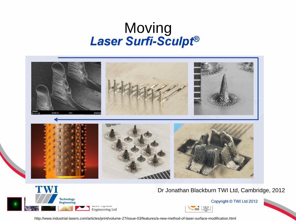
Dr Jonathan Blackburn TWI Ltd, Cambridge, 2012
http://www.industrial-lasers.com/articles/print/volume-27/issue-03/features/a-new-method-of-laser-surface-modification.html
Moving

Cleaning

Addition (and welding)

Laser marking
14
○ Most systems have ‘2.5D’, some vertical movement but limited ability to stitch areas across a complex surface
Videos: EOX lasers; Keyence

What is marking? ○ Black mark
○ Deep burn
○ White mark
○ Surface ‘scratching’
○ Annealing
○ Multiple layers giving colour
○ Ablation
○ Removal of material

Ablation: Excimer machining
https://www.researchgate.net/profile/Salem_Saadon/publication/2832
78426/figure/fig-4Images-of-excimer-laser-cuts-on-four-materials-
6.png

Metal gratings

Laser measuring
• Point or line
• Build up a series of
measurements
• Transform into a
surface
– Roughness
– Profile/shape

Laser shearography
• Testing for internal
defects in composite
and coated structures
– delamination
– Disbonds
– Damage
– Blistering

Object of the Project
○ MCL are pushing the limits of their current technology to achieve OEMs requirements
○ Some foreign technology (LPKF) is able to partially meet foreseen challenges
○ Approached LOE to see if we could work with them to do something better
20
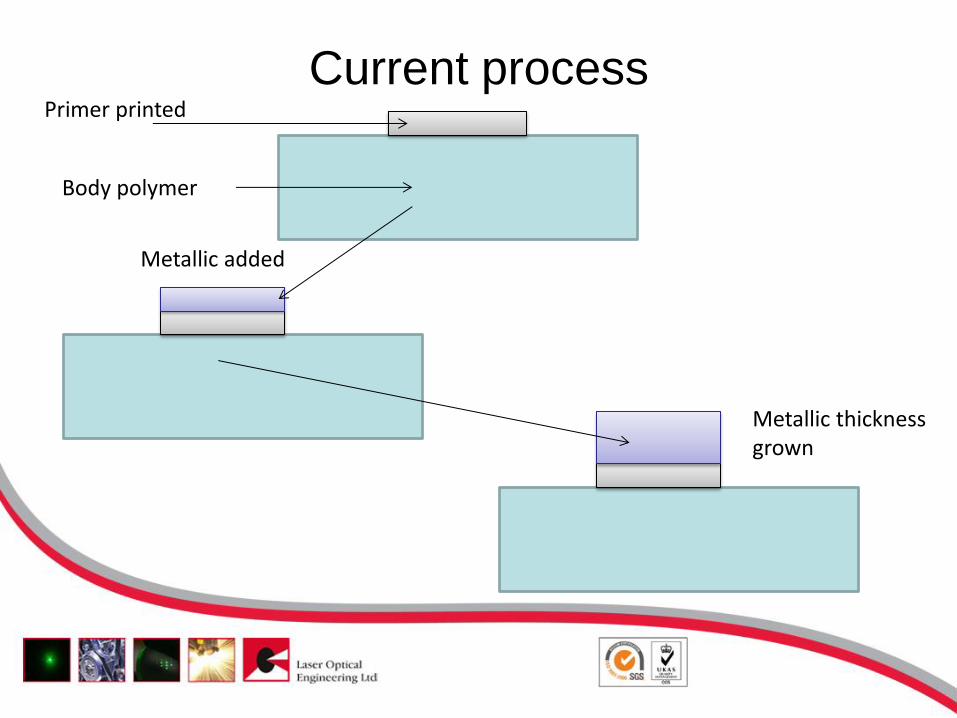
Current process Primer printed
Body polymer
Metallic added
Metallic thickness grown
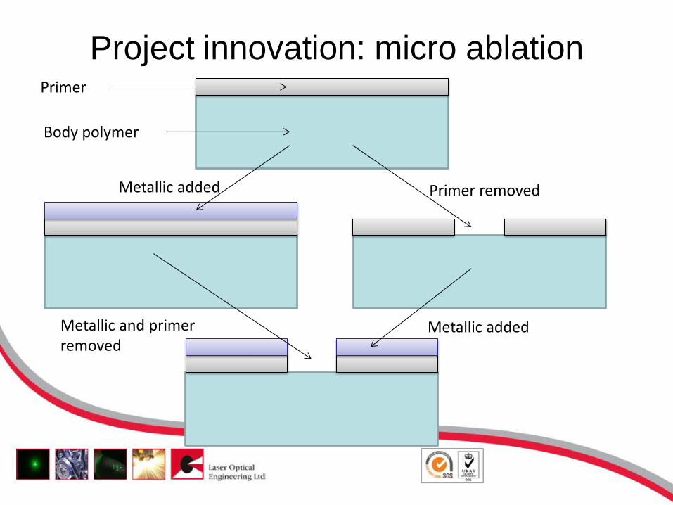
Project innovation: micro ablation Primer
Body polymer
Metallic added
Metallic and primer removed
Primer removed
Metallic added
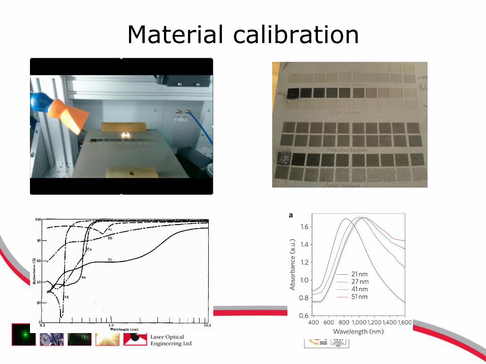
Material calibration
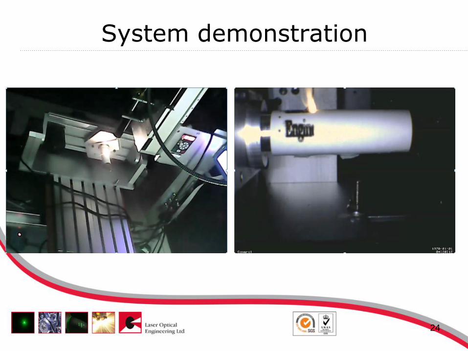
System demonstration
24

What can we offer?
○ Rapid manufacturing of 3D metallic tracks.
○ Tailoring process for track formation on a range of polymeric surfaces.
○ Supply of complete part from customers design or patterning of customer manufactured part
○ We can create brand new markets e.g. by functionalising carbon fibre structural components.
25

What have we achieved? ○ New system capable producing complex finishes on parts
○ A method of producing electronic functionality onto the surface of 3D structural components.
○ Ability to reduce part count and simplify structures by combining electronic and structural parts
○ More energy efficient manufacturing of multi-functional components
○ Electronics manufacturers will realise designs that were previously uneconomical or impossible to produce
26

Where now?
○ Current system is a development prototype
○ LOE intend to use this to work with MCL to optimise processes
○ MCL well placed to exploit outcomes
○ Known in market
○ Customer contacts and relationships
○ Have design expertise and coating capability across a wide range of materials and
○ Thanks to NATEP funding scheme MAA045
www.natep.org.uk
27

www.natep.org.uk
Project Partners :- Moulded Circuits Limited Laser Optical Engineering MBDA
3D Moulded Circuits MAA 045

Contact details
29 www.natep.org.uk
Pete Stone MOULDED CIRCUITS Ltd 1142 Melton Road Syston Leicestershire LE7 2HA Tel: 0116 260 9841 Fax: 01162698392 [email protected]
Daniel Lloyd LOE Unit 72A Argosy Road East Midlands Aiport De74 2SA 01332 814612 [email protected]