Laser Metallization And Doping For Silicon Carbide Diode ...
195
University of Central Florida University of Central Florida STARS STARS Electronic Theses and Dissertations, 2004-2019 2006 Laser Metallization And Doping For Silicon Carbide Diode Laser Metallization And Doping For Silicon Carbide Diode Fabrication And Endotaxy Fabrication And Endotaxy Zhaoxu Tian University of Central Florida Part of the Materials Science and Engineering Commons Find similar works at: https://stars.library.ucf.edu/etd University of Central Florida Libraries http://library.ucf.edu This Doctoral Dissertation (Open Access) is brought to you for free and open access by STARS. It has been accepted for inclusion in Electronic Theses and Dissertations, 2004-2019 by an authorized administrator of STARS. For more information, please contact [email protected]. STARS Citation STARS Citation Tian, Zhaoxu, "Laser Metallization And Doping For Silicon Carbide Diode Fabrication And Endotaxy" (2006). Electronic Theses and Dissertations, 2004-2019. 872. https://stars.library.ucf.edu/etd/872
Transcript of Laser Metallization And Doping For Silicon Carbide Diode ...

University of Central Florida University of Central Florida
STARS STARS
Electronic Theses and Dissertations, 2004-2019
2006
Laser Metallization And Doping For Silicon Carbide Diode Laser Metallization And Doping For Silicon Carbide Diode
Fabrication And Endotaxy Fabrication And Endotaxy
Zhaoxu Tian University of Central Florida
Part of the Materials Science and Engineering Commons
Find similar works at: https://stars.library.ucf.edu/etd
University of Central Florida Libraries http://library.ucf.edu
This Doctoral Dissertation (Open Access) is brought to you for free and open access by STARS. It has been accepted
for inclusion in Electronic Theses and Dissertations, 2004-2019 by an authorized administrator of STARS. For more
information, please contact [email protected].
STARS Citation STARS Citation Tian, Zhaoxu, "Laser Metallization And Doping For Silicon Carbide Diode Fabrication And Endotaxy" (2006). Electronic Theses and Dissertations, 2004-2019. 872. https://stars.library.ucf.edu/etd/872
LASER METALLIZATION AND DOPING FOR SILICON CARBIDE DIODE FABRICATION AND ENDOTAXY
by
ZHAOXU TIAN B.S. Northwestern Polytechnical University, 1996
M.S. University of Science and Technology Beijing, 2003
A dissertation submitted in partial fulfillment of the requirements for the degree of Doctor of Philosophy
in the Department of Mechanical, Materials and Aerospace Engineering in the College of Engineering and Computer Science
at the University of Central Florida Orlando, Florida
Spring Term 2006
Major Professor: Aravinda Kar

ii
© 2006 Zhaoxu Tian

iii
ABSTRACT
Silicon carbide is a promising semiconductor material for high voltage, high frequency
and high temperature devices due to its wide bandgap, high breakdown electric field
strength, highly saturated drift velocity of electrons and outstanding thermal conductivity.
With the aim of overcoming some challenges in metallization and doping during the
fabrication of silicon carbide devices, a novel laser-based process is provided to direct
metallize the surface of silicon carbide without metal deposition and dope in silicon
carbide without high temperature annealing, as an alternative to the conventional ion
implantation, and find applications of this laser direct write metallization and doping
technique on the fabrication of diodes, endotaxial layer and embedded optical structures
on silicon carbide wafers.
Mathematical models have been presented for the temperature distributions in the wafer
during laser irradiation to optimize laser process parameters and understand the doping
and metallization mechanisms in laser irradiation process.
Laser irradiation of silicon carbide in a dopant-containing ambient allows to
simultaneously heating the silicon carbide surface without melting and incorporating
dopant atoms into the silicon carbide lattice. The process that dopant atoms diffuse into
the bulk silicon carbide by laser-induced solid phase diffusion (LISPD) can be explained
by considering the laser enhanced substitutional and interstitial diffusion mechanisms.
Nitrogen and Trimethyaluminum (TMA) are used as dopants to produce n-type and p-
iv
type doped silicon carbide, respectively. Two laser doping methods, i.e., internal heating
doping and surface heating doping are presented in this dissertation. Deep (800 nm doped
junction for internal heating doping) and shallow (200 nm and 450 nm doped junction for
surface heating doping) can be fabricated by different doping methods. Two distinct
diffusion regions, near-surface and far-surface regions, were identified in the dopant
concentration profiles, indicating different diffusion mechanisms in these two regions.
The effective diffusion coefficients of nitrogen and aluminum were determined for both
regions by fitting the diffusion equation to the measured concentration profiles. The
calculated diffusivities are at least 6 orders of magnitude higher than the typical values
for nitrogen and aluminum, which indicate that laser doping process enhances the
diffusion of dopants in silicon carbide significantly. No amorphization was observed in
laser-doped samples eliminating the need for high temperature annealing.
Laser direct metallization can be realized on the surface of silicon carbide by generating
metal-like conductive phases due to the decomposition of silicon carbide. The ohmic
property of the laser direct metallized electrodes can be dramatically improved by
fabricating such electrodes on laser heavily doped SiC substrate.
This laser-induced solid phase diffusion technique has been utilized to fabricate
endolayers in n-type 6H-SiC substrates by carbon incorporation. X-ray energy dispersive
spectroscopic analysis shows that the thickness of endolayer is about 100 nm. High
resolution transmission electron microscopic images indicate that the laser endotaxy
process maintains the crystalline integrity of the substrate without any amorphization.

v
Rutherford backscattering studies also show no amorphization and evident lattice
disorder occur during this laser solid phase diffusion process. The resistivity of the
endolayer formed in a 1.55 Ω·cm silicon carbide wafer segment was found to be 1.1 ×10⁵
Ω ·cm which is sufficient for device fabrication and isolation. Annealing at 1000°C for 10
min to remove hydrogen resulted in a resistivity of 9.4 ×10⁴ Ω ·cm.
Prototype silicon carbide PIN diodes have been fabricated by doping the endolayer and
parent silicon carbide epilayer with aluminum using this laser-induced solid phase
diffusion technique to create p-regions on the top surfaces of the substrates. Laser direct
metallized contacts were also fabricated on selected PIN diodes to show the effectiveness
of these contacts. The results show that the PIN diode fabricated on a 30 nm thick
endolayer can block 18 V, and the breakdown voltages and the forward voltages drop at
100 A/cm2 of the diodes fabricated on 4H-SiC with homoepilayer are 420 ~ 500 V and
12.5 ~ 20 V, respectively.
The laser direct metallization and doping technique can also be used to synthesize
embedded optical structures, which can increase 40% reflectivity compared to the parent
wafer, showing potential for the creation of optical, electro-optical, opto-electrical, sensor
devices and other integrated structures that are stable in high temperature, high-pressure,
corrosive environments and deep space applications.

vi
To my parents, Songlin Tian and Shuilian Yin, and wife Qianqian Hu.
Thank you

vii
ACKNOWLEDGMENTS
I would like to thank for those who contributed and supported throughout my graduate
studies at the College of Optics & Photonics/CREOL and Department of Mechanical,
Materials and Aerospace Engineering. First of all I would like to express my heartfelt
gratitude to my advisor, Dr. Aravinda Kar, for his guidance, advice and support. His
advisement, discussion, encouragement and suggestions have given me the confidence
and success in my daily practice and made this work possible. Thanks to him, I learned
not only how to manage difficulties and accomplish challenging research projects but
also how to think independently and creatively. I am also grateful to Dr. N. Quick,
president of AppliCote Associates, for his support and encouragement. Dr. Quick’s
experience had contributed generously to the success of my research work.
I would like to thank my committee members: Dr. G. Braunstein, Dr. D. Malocha, Dr. W.
Schoenfeld, Dr. C. Suryanaryana and Dr. R. Vaidyanathan for their time reviewing my
dissertation and for their valuable comments and discussions. Thanks are also due to the
technical staff at MCF for their help in the materials characterization work. I would like
to express my appreciations to all colleagues in the LAMP group. Finally I would like to
thank my family and friends for their love, understanding and support through the years.

viii
TABLE OF CONTENTS
LIST OF FIGURES .......................................................................................................... xii
LIST OF TABLES........................................................................................................... xix
LIST OF ACRONYMS/ABBREVIATIONS.................................................................. xxi
LIST OF PUBLICATIONS ........................................................................................... xxvi
CHAPTER 1: INTRODUCTION AND LITERATURE REVIEW ................................... 1
1.1 Motivation........................................................................................................... 1
1.2 Literature Reviews .............................................................................................. 3
1.2.1 Silicon Carbide............................................................................................ 3
1.2.2 Current Technology Barriers in Silicon Carbide Device Fabrication......... 5
1.2.3 Fabrication of Silicon Carbide PIN Diodes .............................................. 14
1.2.4 Epitaxial Growth of Silicon Carbide......................................................... 16
1.2.5 Laser Interaction with Semiconductors .................................................... 19
1.2.6 Temperature Distribution during Laser Irradiation Process ..................... 21
1.3 Objectives ......................................................................................................... 22
CHAPTER 2: TEMPERATURE DISTRIBUTION ANALYSIS DURING LASER
METALLIZATION AND DOPING PROCESS OF SILICON CARBIDE..................... 24
2.1 Introduction....................................................................................................... 24
2.2 Mathematical model and analysis of laser internal heating .............................. 26
2.2.1 Mathematical model and solution............................................................. 26
2.2.2 Results and Discussion ............................................................................. 29
2.3 Mathematical model and analysis of surface heating ....................................... 46

ix
2.3.1 Mathematical Model and Solution............................................................ 46
2.3.2 Results and discussion .............................................................................. 47
CHAPTER 3: EXPERIMENTAL METHODS AND CHARACTERIZATION
TECHNIQUES ................................................................................................................. 53
3.1 Samples Preparation.......................................................................................... 53
3.2 Laser Irradiation Experimental Set-up.............................................................. 54
3.3 Materials Characterization ................................................................................ 58
3.3.1 Secondary Ion Mass Spectroscopy (SIMS) .............................................. 58
3.3.2 Focused Ion Beam Instrument (FIB) ........................................................ 58
3.3.3 Transmission Electron Microscopy (TEM) .............................................. 59
3.3.4 X-ray Energy Dispersive Spectrometry (XEDS)...................................... 59
3.3.5 Rutherford Backscattering Spectroscopy (RBS) ...................................... 59
3.4 Electrical Characterization................................................................................ 60
3.4.1 Current-Voltage (I-V) Characteristics of the Laser Direct Metallized
Electrodes.................................................................................................................. 60
3.4.2 Resistivity of the Endolayer...................................................................... 60
3.4.3 Current-Voltage (I-V) Characteristics of the PIN Diodes ........................ 61
3.5 Optical Characterization ................................................................................... 61
3.5.1 Laser Beam Characteristics....................................................................... 61
3.5.2 Reflectivity and Transmitivity of Optical Structure at Particular
Wavelength ............................................................................................................... 61
CHAPTER 4: LASER DOPING AND DIRECT METALLIZATION OF SILICON
CARBIDE......................................................................................................................... 62

x
4.1 Introduction....................................................................................................... 62
4.2 Laser Doping Process of Silicon Carbide ......................................................... 63
4.3 Doping profiles ................................................................................................. 71
4.3.1 Doping Profiles Obtained by Laser Internal Heating ............................... 71
4.3.2 Doping profiles obtained by Laser Surface Heating................................. 76
4.4 Mechanisms of Laser Doping Process.............................................................. 78
4.5 Effective Diffusivity Analysis .......................................................................... 80
4.6 Laser Metallization Process of Silicon Carbide................................................ 93
4.7 Realization of Laser Direct Metallization on the Surface of Silicon Carbide .. 96
CHAPTER 5: FABRICATION OF ENDOLAYER AND PIN DIODES OF SILICON
CARBIDE....................................................................................................................... 102
5.1 Introduction..................................................................................................... 102
5.2 Fabrication of Endolayers in N-Type 6H-SiC Substrates............................... 103
5.2.1 Experimental Procedures ........................................................................ 103
5.2.2 Carbon Source......................................................................................... 104
5.2.3 Hydrogen removal from the endolayer ................................................... 107
5.2.4 Determination of the Thickness and Crystalline Order of the Endolayer109
5.2.5 Determination of the Resistivity of the Endolayer ................................. 119
5.3 Fabrication of PIN Diodes on Substrates with an Endolayer ......................... 123
5.4 Fabrication of PIN Diodes on Substrates with Epilayer ................................. 129
CHAPTER 6: LASER SYNTHESIS OF OPTICAL STRUCTURE IN SILICON
CARBIDE....................................................................................................................... 139
6.1 Introduction..................................................................................................... 139

xi
6.2 Laser Synthesis of Embedded Optical Phases ................................................ 139
6.3 Optical Property Modification ........................................................................ 144
CHAPTER 7: SUMMARY............................................................................................. 150
7.1 Conclusions..................................................................................................... 150
7.2 Future Work .................................................................................................... 153
REFERENCES ............................................................................................................... 155
xii
LIST OF FIGURES
Figure 1.1 A schematic of doping by ion implantation [Singh (2001)].............................. 9
Figure 1.2 Illustration of GILD process [Jones et al. (1998)]........................................... 13
Figure 1.3 Cross-sectional structure of 4H-SiC UHV diode with shallow mesa JTE
[Sugawara et al. (2001)]............................................................................................ 15
Figure 2.1 Different heating mechanisms for laser irradiation: (a) Volumetric heating
during Nd:YAG laser irradiation and (b) Surface heating during excimer laser
irradiation.................................................................................................................. 25
Figure 2.2 Transient temperature distribution along the depth of the substrate (d = 270
μm) at t = 48 ns during Nd:YAG laser irradiation. The laser irradiance = 80.6
MW/cm2, beam radius = 150 μm, pulse length = 72 ns and pulse repetition rate = 3
kHz............................................................................................................................ 31
Figure 2.3 Temperature distribution of 6H-SiC wafer (d = 430 μm) irradiated at different
laser intensity (I=50, 100 and 150 MW/cm2) and same pulse repetition rate (f=3
kHz) and accordingly pulse on time (τon=72 ns). ..................................................... 33
Figure 2.4 Temperature distribution of 6H-SiC wafer (d = 430 μm) irradiated at different
pulse repetition rate (f=3, 10, 20 and 35 kHz) and pulse on time (τon =72, 126, 200
and 290 ns) and same laser intensity (I=50 MW/cm2).............................................. 34
Figure 2.5 Variation of peak temperature with laser intensity at different pulse repetition
rate (f=3, 10, 20, 35 kHz) on the 6H-SiC substrate (d = 430 μm). ........................... 35

xiii
Figure 2.6 Variation of peak temperature for 4H- and 6H-SiC at the combination of laser
intensity and pulse repetition rate. The curves indicating the decomposition
temperature of SiC, 3100 K. ..................................................................................... 36
Figure 2.7 Temperature distribution of one single pulse with same peak temperature
(3100 K) irradiated at different pulse repetition rate (f=3, 17.5 and 35 kHz) and laser
intensity (I=88.7, 56.4 and 44.2 MW/cm2) on 6H-SiC substrate (d = 430 μm). ...... 39
Figure 2.8 Variation of temperature at the end of one single pulse with pulse repetition
rate for 4H- and 6H- SiC wafers (d = 430 μm)......................................................... 40
Figure 2.9 Temperature profiles of three pulses of 6H-SiC wafer (d = 430 μm) irradiated
at pulse repetition rate of 3 kHz and laser intensity of 88.7 MW/cm2...................... 41
Figure 2.10 Temperature profiles of three pulses of 6H-SiC wafer (d = 430 μm) irradiated
at pulse repetition rate of 17.5 kHz and laser intensity of 56.4 MW/cm2................. 42
Figure 2.11 Temperature profiles of three pulses of 6H-SiC wafer (d = 430 μm) irradiated
at pulse repetition rate of 35 kHz and laser intensity of 44.2 MW/cm2.................... 43
Figure 2.12 Time evolution of temperature along the thickness of the 6H-SiC wafer (d =
430 μm) near the bottom surface region. (Laser intensity: 91 MW/cm2; Pulse
repetition rate: 3 kHz). .............................................................................................. 44
Figure 2.13 Temperature profiles of 6H-SiC (d = 430 μm) at particular position during
the laser irradiation. (Laser intensity: 91 MW/cm2; Pulse repetition rate: 3 kHz). .. 45
Figure 2.14 Temperature profiles of 6H-SiC irradiated by different excimer laser sources
(λ=351, 248 and 193 nm) and same laser intensity (60 MW/cm2). .......................... 50

xiv
Figure 2.15 Temperature profiles of 4H-SiC irradiated by different excimer laser sources
(λ=351, 248 and 193 nm) and same laser intensity (60 MW/cm2). .......................... 51
Figure 2.16 Time evolution of temperature along the thickness of the 6H-SiC wafer near
the top surface region. (Laser intensity: 73 MW/cm2; wavelength: 248 nm). .......... 52
Figure 3.1 Intensity profile of the incident Nd:YAG laser beam. (a) Front view. (b) Top
view........................................................................................................................... 55
Figure 3.2 Experimental set-up for laser doping, direct metallization and growing
endolayer system....................................................................................................... 57
Figure 4.1 Temperature distribution of 6H-SiC during n-type doping using the parameters
of method A listed in Table 4.1.(a) Bottom surface temperature distribution with the
time; (b) Transient temperature distribution along the thickness of the wafer from
the bottom surface at the peak temperature (t=48ns)................................................ 66
Figure 4.2 Temperature distribution of 6H-SiC during p-type doping using the parameters
of method A listed in Table 4.1.(a) Bottom surface temperature distribution with the
time; (b) Transient temperature distribution along the thickness of the wafer from
the bottom surface at the peak temperature (t=48ns)................................................ 68
Figure 4.3 Temperature distribution of 4H-SiC during p-type doping using the parameters
of method C listed in Table 4.1.(a) Top surface temperature distribution with the
time; (b) Transient temperature distribution along the thickness of the wafer from
the top surface at the peak temperature (t=25ns). ..................................................... 70
Figure 4.4 Nitrogen dopant profiles obtained with a Nd:YAG laser. Ca: Concentration of
nitrogen in the as-received wafer; Cd: Concentration of nitrogen in the doped wafer.
................................................................................................................................... 73

xv
Figure 4.5 Concentration depth profiles of aluminum doped by LISPD method measured
with SIMS. ................................................................................................................ 74
Figure 4.6 Comparison of concentration of Al and N2 dopants along the depth of 6H-SiC
wafer using similar laser doping parameters. ........................................................... 75
Figure 4.7 Aluminum dopant profiles obtained with an excimer laser. Ca: Concentration
of aluminum in the as-received wafer; Cd1: Concentration of aluminum in the 1000
laser pulses doped wafer; Cd2: Concentration of aluminum in the 3000 laser pulses
doped wafer............................................................................................................... 77
Figure 4.8 Comparison between the diffusion theory and experimental data for a selected
diffusion coefficient in the case of Nd:YAG laser doping of nitrogen in 6H-SiC. .. 89
Figure 4.9 Comparison between the diffusion theory and experimental data for a selected
diffusion coefficient in the case of KrF excimer laser doping of aluminum in 4H-
SiC............................................................................................................................. 90
Figure 4.10 Temperature distribution of 6H-SiC during laser direct metallization using
the parameters listed in Table 4.4.(a) Bottom surface temperature distribution with
the time; (b) Transient temperature distribution along the thickness of the wafer
from the bottom surface at the peak temperature (t=48ns). ...................................... 95
Figure 4.11 Electrode structures in n-type 6H-SiC substrates by different processing: (a)
laser direct metallized contacts fabricated on laser heavily doped n+ substrate
(specimen A); (b) laser direct metallized contacts fabricated on original substrate
(specimen B); (c) Ni contacts deposited on original substrate (specimen C). .......... 97
Figure 4.12 Current- voltage characteristics between two electrodes on the SiC substrates
formed by different methods at room temperature. ................................................ 100
xvi
Figure 4.13 Current- voltage characteristics between two electrodes on the SiC substrates
formed by different methods at elevated temperatures: (a) 150 °C; (b) 250 °C..... 101
Figure 5.1 Comparison of the hydrogen content in a 6H-SiC sample of three different
qualities. .................................................................................................................. 108
Figure 5.2 XEDS analysis for the carbon contents along the depth of both annealed
endolayer specimen and parent wafer: (a) XEDS scanning line showing four
locations a, b, c and d along the depth of the endolayer specimen; (b) XEDS
scanning line showing four locations a, b, c and d along the depth of the parent
specimen; (c) XEDS data for carbon counts along the depth of the specimens. The
four locations a, b, c and d are marked on these data to show higher carbon content
in the endolayer than in the parent specimen, indicating carbon incorporation into
the wafer during the endotaxy experiment.............................................................. 111
Figure 5.3 TEM images of cross-sections of an annealed endolayer and parent wafer: (a)
Observed amorphous layer in the endolayer specimen; (b) Observed amorphous
layer in the parent wafer. ........................................................................................ 113
Figure 5.4 High-resolution TEM images of cross-sections of an annealed endolayer and
parent wafer: (a) The interface between damaged amorphous and crystalline SiC of
the endolayer specimen; (b) The interface between damaged amorphous and
crystalline SiC of the parent wafer.......................................................................... 114
Figure 5.5 The aligned and random RBS channeling spectra of parent 6H-SiC sample.116
Figure 5.6 The aligned and random RBS channeling spectra of endolayer specimen. .. 117
Figure 5.7 The aligned and random RBS channeling spectra of annealed endolayer
specimen. ................................................................................................................ 118
xvii
Figure 5.8 Typical range of resistivities for insulators, semiconductors and conductors.
................................................................................................................................. 122
Figure 5.9 Device designs on SiC substrates with and without an endolayer: (a) PIN
diode on laser-formed endolayer and (b) reference p-n junction............................ 125
Figure 5.10 Depth profiles of aluminum concentration in the top laser-doped p region in
the endolayer measured by SIMS. .......................................................................... 127
Figure 5.11 I-V characteristics of PIN diodes fabricated on an endolayer and a parent 6H-
SiC........................................................................................................................... 128
Figure 5.12 Cross-sectional views of the laser fabricated PIN diodes and referenced
Schottky diode. (a) Diode A, with just top laser doped p region; (b) Diode B, with
both top laser doped p region (200 nm junction depth) and bottom n+ region; (c)
Diode C, with both top laser doped p+/p region (450 nm junction depth) and bottom
n+ region; and (d) Diode D, reference Schottky diode........................................... 130
Figure 5.13 Temperature distribution of 4H-SiC during laser direct metallization using
the parameters listed in Table 5.4.(a) Bottom surface temperature distribution with
the time; (b) Transient temperature distribution along the thickness of the wafer
from the bottom surface at the peak temperature (t=48ns). .................................... 133
Figure 5.14 Measured Schottky diode and PIN diodes I-V curves at room temperature. (a)
Schottky diode. (b) Laser fabricated PIN diodes. ................................................... 137
Figure 6.1 Fabrication of an embedded optical structure. .............................................. 142
Figure 6.2 Silicon carbide substrate showing an embedded optical structure. ............... 143
Figure 6.3 Experimental set-up for measuring the reflectivity and transmission of laser
synthesized optical structures at particular wavelength.......................................... 145

xviii
Figure 6.4 Reflectivity of parent wafer, C rich phase, C rich phase containing N2 and C
rich phase containing Al measured at 1064 nm. ..................................................... 148
Figure 6.5 Transmission of parent wafer, C rich phase, C rich phase containing N2 and C
rich phase containing Al measured at 1064 nm. ..................................................... 149

xix
LIST OF TABLES
Table 1.1 Comparison of electrical properties of SiC, Si and GaAs [Heft et al. (1995),
Zetterling, et al. (2002) and Goldberg et al. (2001)]................................................... 7
Table 1.2 Overview of epitaxy techniques [Stringfellow, (1999)] .................................. 18
Table 2.1 The properties and parameters of the SiC wafer used in this study.................. 30
Table 2.2 Absorption and heat transfer coefficients of 4H- and 6H-SiC [Levinshtein et al.
(2001)]....................................................................................................................... 48
Table 3.1 Silicon carbide samples used in this study........................................................ 53
Table 4.1 Processing parameters for different laser doping methods.............................. 65
Table 4.2 Fitting parameters used in Eqs. 4.32 and 4.33 to compare the theory with
experimental dopant profiles in Figs. 4.8 and 4.9 for determining the effective
diffusivity.................................................................................................................. 91
Table 4.3 Comparison of diffusion coefficients in conventional and laser doping
processes for different impurities in SiC and Si. ...................................................... 92
Table 4.4 Processing parameters for laser direct metallization. ....................................... 94
Table 5.1 Laser processing parameters for endotaxy experiments. ................................ 105
Table 5.2 Resistances and resistivities of parent sample, endolayer and annealed
endolayer................................................................................................................. 121
Table 5.3 Laser processing parameters for p-type doping on the endolayer and parent
substrate. ................................................................................................................. 124

xx
Table 5.4 Laser processing parameters for p-type doping and laser direct metallization on
the Diodes shown in Fig. 5.12. ............................................................................... 131
Table 5.5 Comparison of the performance of the PIN diodes fabricated in the literatures
and our group. ......................................................................................................... 138
Table 6.1 Laser processing parameters for the synthesis of embedded optical phases. . 140
Table 6.2 Reflectivity and transmission calculation of laser synthesized optical structure
................................................................................................................................. 147

xxi
LIST OF ACRONYMS/ABBREVIATIONS
A Absorbance of the SiC substrate
Ali Aluminum atoms at the interstitial sites
ANi Area of the top Ni contact on the endolayer
AlSi Aluminum occupying the lattice site of silicon
BOE Buffered oxide etch
Ca Concentration of dopants in the as-received wafer
C0 Dopant concentration at the wafer surface
C1 Characteristic concentration representing the diffusion process in the far-
surface region
Cd Concentration of nitrogen in the doped wafer
Cd1 Concentration of aluminum in the 1000 laser pulses doped wafer
Cd2 Concentration of aluminum in the 3000 laser pulses doped wafer
CIVPE Chloride Vapor-phase Epitaxy
Cp Specific heat capacity at constant pressure
CVD Chemical Vapor Deposition
CW Continuous wave
D Diffusion coefficient
D. I. Deionized
D0 Mass diffusivity
∗0D Pre-exponential factor
Dfs Average diffusion coefficient in the far-surface region

xxii
DPBs Double positioning boundaries
d Wafer thickness
de Thickness of the endolayer
d ′ Distance the laser beam travels in the wafer
d* Distance that the laser beam travels from the beam incident side of the
wafer to the top of the embedded structure
CE Critical electric field
Ep Pulse energy
f Pulse repetition rate
FIB Focused Ion Beam Instrument
g Heat source
GILD Gas immersion laser doping
HVPE Hydride Vapor-phase Epitaxy
I Current
Il Laser irradiance
Ip Pulse intensity
JTE Junction termination extension
k Thermal conductivity
kB Boltzmann constant
LCVD Laser Chemical Vapor Deposition
LISPD Laser-induced solid-phase doping
Lm Mass diffusion length
LPE Liquid phase epitaxy

xxiii
LTP Laser thermal processing
MBE Molecular beam epitaxy
MJTE Multistep junction termination extension.
Nc Nitrogen occupying the lattice site of carbon
Ni Nitrogen atoms at the interstitial sites
Nv Vacancy concentration
OMVPE Organometallic Vapor-Phase Epitaxy
P0 Incident laser power
PLA Pulsed laser annealing
PLD Pulsed laser doping
PLIE Pulsed laser induced epitaxy
PMOS Positive Channel Metal Oxide Semiconductor
PR Reflected laser power
Pr Pulse repetition rate
PT Transmitted laser power
Q Activation energy
q Electronic charge
rc Contact resistance
r0 Laser beam radius
R Reflectance (Reflectivity) of the SiC substrate
Rtotal Resistances of the endolayer samples
Rc Resistances of the contacts
Re Resistances of the endolayer

xxiv
Rs Resistances of the substrate
RBS Rutherford Backscattering Spectroscopy
rc Specific contact resistance
RL Reflectivity of the laser synthesized structures
RTA Rapid thermally annealing
SBH-φB Schottky Barrier Height
SIMS Secondary Ion Mass Spectroscopy
SPE Solid phase epitaxy
T Temperature
T0 Initial temperature of the substrate
TA Activation temperature for the diffusion process
TEM Transmission Electron Microscopy
tirr Total laser irradiation time (pulse-on plus pulse-off times)
TL Transmission of the laser synthesized structures
TMA Trimethyaluminum
ton Pulse length (pulse-on time)
t ′ Diffusion time in the far-surface region
v Laser scanning speed
V Voltage
BV Breakdown voltage
Vc Carbon vacancies
VSi Silicon vacancies
VPE Vapor phase epitaxy

xxv
ND Dopant concentration
UHV Ultrahigh-vacuum
W Drift layer thickness
XEDS X-ray Energy Dispersive Spectrometry
Greek Symbols
α Thermal diffusivity
σ Electric conductivity
ρ Density
ρe Resistivities of the endolayers
λ Wavelength
η Absorption coefficient of the original wafer
φB Schottky Barrier Height
φp Pulse fluence
φth Threshold ion dose
τon Pulse-on time
ε Dielectric constant
0ε Permittivity of vacuum,
rε Relative dielectric constant of SiC

xxvi
LIST OF PUBLICATIONS
Journal Papers
1. Z. Tian, N.R. Quick and A. Kar, Laser Enhanced Diffusion of Nitrogen and Aluminum
Dopants in Silicon Carbide, submitted to Acta Materialia.
2. Z. Tian, N.R. Quick and A. Kar, Laser Endotaxy and PIN Diode Fabrication of Silicon
Carbide, submitted to Journal of Electronic Materials.
3. Z. Tian, I.A. Salama, N.R. Quick and A. Kar, Effect of Different Laser Sources and
Doping Methods Used to Dope Silicon Carbide, Acta Materialia, Vol. 53, 2005, pp.
2835- 2844.
4. Z. Tian, N.R. Quick and A. Kar, Characteristics of 6H-Silicon Carbide PIN
Diodes Prototyping by Laser Doping, Journal of Electronic Materials, Vol. 34,
2005, pp. 430-438.
Conference Papers
1. Z. Tian, N.R. Quick and A. Kar, Laser Endotaxy and PIN Diode Fabrication of Silicon
Carbide, Symposium B: Silicon Carbide ⎯ Materials, Processing and Devices, edited
by M. A. Capano, M. Dudley, T. Kimoto, A. R. Powell and S. Wang, (San Francisco,
California, 2006), B10.7.
2. Z. Tian, N.R. Quick and A. Kar, Laser Direct Write Doping and Metallization
Fabrication of Silicon Carbide PIN Diodes, in International Conference on Silicon
Carbide Related Metarials Proc., Pittsburgh, PA, 2005.

xxvii
3. Z. Tian and A. Kar, Nd:YAG Laser Surface Treatment of Coating on Polyimide
Substrate, ICALEO (International Congress on Applications of Lasers and Electro-
Optics), Miami, Florida, 2005.
4. Z. Tian, N.R. Quick and A. Kar, Fabrication of Silicon Carbide PIN Diodes by Laser
Doping and Planar Edge Termination by Laser Metallization, Symposium E:
Semiconductor Defect Engineering ⎯ Materials, Synthetic Structures and Devices,
edited by S. Ashok, J. Chevallier, B.L. Sopori, M. Tabe and P. Kiesel, (Mater. Res.
Soc. Symp. Proc. 864, San Francisco, California, 2005), E9.3.
5. Z. Tian, N.R. Quick and A. Kar, Laser-Synthesis of Optical Structures in Silicon
Carbide, in Symposium “State-of-the-Art Program on Compound Semiconductors
SLII”, 207th Meeting of the Electrochemical Society, (Quebec City, Canada, May 15-
20, 2005).
6. Z. Tian, N.R. Quick and A. Kar, Laser Doping of Silicon Carbide and PIN Diode
Fabrication, in Proceeding of the 23rd International Congress on Application of Laser
& Electro-Optics, (San Fransicso, California, October 4-7, 2004), M306.
7. Z. Tian, N.R. Quick and A. Kar; Laser Direct Write and Gas Immersion Laser Doping
Fabrication of SiC diodes, in Silicon Carbide 2004-Materials Processing and Devices,
edited by Michael Dudley, Perena Gouma, Tsunenobu Kimoto, Philip G. Neudeck, and
Stephen E. Saddow (Mater. Res. Soc. Symp. Proc. 815, Warrendale, PA, 2004), J3.4
8. Z. Tian, N.R. Quick and A. Kar, Laser Direct Metallization and Doping of 6H-SiC,
Session III: Electronic Materials, Annual Joint Symp. Florida Society for Microscopy
and Florida Chapter of the American Vacuum Society, Orlando, Florida, March 8-9,
2004 (invited presentation).

1
1 CHAPTER 1: INTRODUCTION AND LITERATURE REVIEW
1.1 Motivation
Silicon carbide (SiC) is a promising semiconductor material for high-voltage, high-
frequency and high-temperature devices due to its wide bandgap (2.36-3.5 eV), high
breakdown electric field strength (3-5 MV/cm), high saturated drift velocity of electrons
(2×107 cm/s) and high thermal conductivity (350-490 Wm-1K-1) [Heft et. al (1995) and
Levinshtein et. al (2001)].
However, there are still technology barriers for silicon carbide device fabrication
including micropipe defects in the substrate and processing limitations (e.g., dielectric
deposition, etching, oxidation, metallization, and doping). One of these challenges is
metallization for source, drain and gate contacts on devices. Metal conductors generate
strains due to thermal expansion coefficient mismatch resulting in debonding, or can
create charge carrier traps, particularly dislocations, which decrease the device efficiency.
Also, metal conductors can oxidize and react with chemical species in hostile
environments degrading their conductive properties and further creating chemical
products that can eventually affect the device [Sengupta et. al (2001)].
Doping is another challenge for SiC device fabrication due to its hardness, chemical
inertness and the low diffusion coefficient of most impurities [Edwards et al. (1997)].

2
Current doping techniques for SiC device fabrication include epilayer doping and ion
implantation. Epilayer doping is in situ doping during chemical vapor deposition (CVD)
epitaxial growth; Nitrogen (N) or phosphorous (P) for n-type, aluminum (Al) or boron
(B) for p-type and vanadium (V) for semi-insulating type are introduced. Ion
implantation is the most common doping technique used for fabricating SiC devices
currently. However, it generates implantation-induced defect centers in the wafer and
therefore, high annealing temperatures are required to remove these defects and to
electrically activate the dopants. Some defects remain in SiC for up to 1700°C annealing
temperatures [Troffer et. al (1997)]. Annealing at these high temperatures can cause
severe surface damage due to Si sublimation and redistribution [Handy et. al (2000)].
With the aim of overcoming some challenges in metallization and doping during the
fabrication of silicon carbide devices, a novel laser direct write technique is provided to
direct metallize the surface of silicon carbide without metal deposition and dope in
silicon carbide instead of conventional ion implantation.
Laser irradiation of SiC in an inert ambient at appropriate processing parameters induces
a conversion in the electric properties by changing the surface stoichiometry at the laser-
irradiated spot. This process forms electrically conductive phases with a metal-like
behavior that can act as either Ohmic or rectifying contact without any metal deposition
with respect to the untreated SiC. It can also serve as interconnects for devices built on
SiC substrate [Salama (2003)].

3
Laser irradiation of SiC in a dopant-containing ambient allows to simultaneously heating
the SiC surface and incorporating dopant atoms into the SiC lattice. This laser doping
process can enhance the dopant diffusivity compared to conventional high temperature
furnace diffusion process and reduce defect generation compared to ion implantation
method. It can also realize selective area doping and dopant and conductivity level
control [Salama (2003)].
1.2 Literature Reviews
1.2.1 Silicon Carbide
As a wide bandgap (2.0 eV ≤ Eg ≤ 7.0 eV) [Casady and Johnson (1996)] semiconductor
material, silicon carbide (SiC) has attracted increasing attention for high-power, high-
frequency, high-temperature and radiation-resistant devices due to its unique structure
and attractive properties.
Silicon carbide is the only chemically stable form of silicon and carbon. The crystalline
structure of SiC can be considered to consist of the close-packed stacking of double
layers of Si and C atoms [Harris (1995)]. The stacking of the double layers follows one of
three possible relative positions, which are arbitrarily labeled A, B and C, each letter
representing a bilayer of individual Si and C atoms. Different stacking sequences of these
three double layers result in SiC’s large number of polytypes. Polytypism is a one-

4
dimensional polymorphism that is a result of the stacking sequence [Harris (1995)].
There are more than 200 different polytypes of SiC crystallizing mainly in three lattice
structures, i.e., cubic, hexagonal and rhombohedral [Pensel and Choyke (1993)]. The
most common polytypes of SiC, which are developed for electronics currently, are 3C-
SiC, 4H-SiC, and 6H-SiC. 3C-SiC with stacking sequence of ABCABC, or known as β-
SiC, is the only polytype of SiC in a cubic lattice structure. Correspondingly, the non-
cubic polytypes of SiC are referred to as α-SiC [Pearton (2000)]. 4H- and 6H-SiC, with
stacking sequences of ABCBABCB and ABCACBABCACB, respectively, are only two
of many possible SiC polytypes with hexagonal crystal structure [Neudeck (2000)].
Different polytypes of SiC have different physical and electronic properties. Among these
three polytypes of SiC presently being developed for electronics, the bandgap energy at
room temperature varies from 2.36 eV for 3C-SiC and 3.0 eV for 6H-SiC to 3.23 eV for
4H-SiC [Goldberg et al. (2001)]. The wide bandgap is the key to almost all advantages of
using SiC in devices. Other important parameters that affect device performance include
electron and hole mobility. 4H-SiC has the highest electron mobility (≤ 900 cm2/Vs) and
3C-SiC has the highest hole mobility (≤ 320 cm2/Vs) and high electron mobility second
to 4H-SiC (≤ 800 cm2/Vs); while 6H-SiC has the lowest electron mobility (≤ 400 cm2/Vs)
and hole mobility (≤ 90 cm2/Vs). Also, the anisotropy of electron mobility in 6H-SiC is
much more than that in 4H-SiC. The ratio of the electron mobility along the normal to the
basal plane (μ⊥) to that in the basal plane (μ//) is about 0.7-0.83 at 300 K in 4H-SiC, while
the same ratio is about 6 in 6H-SiC [Pearton (2000)]. However, the minority carrier

5
lifetime is usually longer in 6H-SiC than in 4H-SiC, which can compensate the low
electron mobility in 6H-SiC for bipolar-type power device applications [Fujihira et al.
(2002)]. Furthermore, the quality and size of 6H-SiC are more advanced than that for 4H-
SiC.
Compared to other semiconductor materials such as silicon and gallium arsenic (GaAs),
SiC has superior properties in many aspects that are crucial for integrated device
fabrication. The comparison of electrical properties of SiC, Si and GaAs is listed in Table
1. SiC’s wide bandgap (2.36-3.23 eV), high breakdown electric field strength (3-5
MV/cm), high saturated drift velocity of electrons (2×107 cm/s) and high thermal
conductivity (350-490 Wm-1K-1) make it an very attractive semiconductor material for
high-power, high- frequency, high-temperature device applications [Heft et al. (1995) and
Goldberg et al. (2001)].
1.2.2 Current Technology Barriers in Silicon Carbide Device Fabrication
There are still some technology barriers for silicon carbide device fabrication such as
dielectric deposition, etching, oxidation, metallization and doping. One of these
challenges is metallization for source, drain and gate contacts on devices.
Metallization Contact in SiC
When a metal and a semiconductor are brought into contact, a rectifying or ohmic contact
can be formed. The critical parameter that determines whether a contact is of ohmic or

6
rectifying nature is the Schottky barrier height (SBH-φB). An ohmic contact requires low
φB while high value of φB is needed for a rectifying contact. An ohmic contact is defined
as having a linear and symmetric current-voltages and an extremely small resistance in
comparison to the bulk of the device. The main purpose of an ohmic contact is to allow
the outside communication of a device. A contact is of rectifying type when it allows
current flow under only one voltage bias regime (positive or negative) and thus becomes
an important factor of the active region of a device [Constantinidis et al. (1997)].
For SiC, most metals can easily form a rectifying contact on SiC, such as Au, Al, Pd, Ni
on n-type SiC and Al, Ni, NiAl, Au on p-type SiC, with low leakage current, low ideality
factor, high breakdown voltage and Schottky barrier height (SBH-φB) in excess of 1 eV
depending on the polytype, doping type and dopant concentration. It is more difficult to
form an ohmic contact on SiC with low contact resistance which may be overcome by
heavy doping of the SiC and using an insulator interlayer to reduce the barrier height and
up to now ohmic contact has been realized on SiC such as Ni, Ti, Mo, Ni-Cr, TiW on n-
type SiC and Al, Ti, Mo, Al-Ti on p-type SiC [Porter et al. (1995)].
However, metal conductors generate strains due to thermal expansion coefficient
mismatch resulting in debonding, or can create charge carrier traps, particularly
dislocations, which decrease the device efficiency. Also, metal conductors can oxidize
and react with chemical species in hostile environments degrading their conductive
properties and further creating chemical products that can eventually affect the device
[Sengupta et al. (2001)].

7
Table 1.1 Comparison of electrical properties of SiC, Si and GaAs [Heft et al. (1995),
Zetterling, et al. (2002) and Goldberg et al. (2001)].
Silicon Carbide
3C-SiC 4H-SiC 6H-SiC
Si GaAs
Energy gap
(eV)
2.36 3.23 3.0 1.12 1.43
Breakdown field
(Mv/cm)
2.0 2.2 2.5 0.25 0.3
Electron saturation velocity (107 cm/sec)
2.5 2.0 2.0 1.0 1.0
Electron mobility
(cm2/Vs) ≤ 800 ≤ 900 ≤ 400 1400 8500
Hole mobility
(cm2/Vs) ≤ 300 ≤ 120 ≤ 90 500 4500
Thermal conductivity (W/cm K)
3.6 3.7 4.9 1.5 0.46
Thermal diffusivity (cm2/s)
1.6 1.7 2.2 0.9 0.24

8
Doping in SiC
Doping is another challenge for SiC device fabrication due to its hardness, chemical
inertness and the low diffusion coefficient of most impurities [Edwards et al. (1997)].
Current doping techniques for SiC device fabrication include epilayer doping and ion
implantation. Epilayer doping is in situ doping during chemical vapor deposition (CVD)
epitaxial growth; Nitrogen (N) or phosphorous (P) for n-type, aluminum (Al) or boron
(B) for p-type and vanadium (V) for semi-insulating type are introduced.
Ion implantation is the most common doping technique used for fabricating SiC devices
currently. This processing is done in ion implanter, one of the most complex
semiconductor processing tools (Fig. 1.1). The basic process of ion implantation is that a
beam of the desired dopant ions, which are created from a source material, extracted and
separated in a mass analyzer, is accelerated in a voltage field to attain a high velocity to
implant the dopants into the semiconductor crystal lattice structure of the target wafer
[Quirk and Serda (2001)]. Implantation is followed by a thermal anneal step to activate
the dopant ions in the crystal structure. In ion implantation, doping concentrations and
doping profiles can be adjusted reproducibly and varied over a wide range; doping
selected areas through masking techniques is possible, which avoids lateral structuring
with wet and dry etching techniques; and basically all stable elements of the periodic
table can be implanted [Zetterling et al. (2002)].

9
Figure 1.1 A schematic of doping by ion implantation [Singh (2001)].
10
However, ion implantation generates implantation-induced defect centers in the wafer
and therefore, high annealing temperatures are required to remove these defects and to
electrically activate the dopants. Some defects remain in SiC for up to 1700°C annealing
temperatures [Troffer et al. (1997)]. Moreover, annealing at these high temperatures can
cause severe surface damage due to Si sublimation and redistribution [Handy et al.
(2000)].
To avoid high temperature annealing after ion implantation, pulsed laser annealing (PLA)
has been used to suppress the ion-implanted defects and electrically activate ion-
implanted dopants. The use of high powerful pulsed laser beams in the nanosecond
duration regime deposits a large amount of energy in very short time into the near-surface
region without evidently affecting the substrate temperature [Dutto et al. (2001)]. Under
different laser processing conditions, irradiation can lead to surface melting of SiC to a
depth of a few hundred nanometers or just annealing in solid phase without surface
melting. The highly non-equilibrium nature of the melt/regrowth process is able to
achieve complete electrical activation of the dopants; while surface degradation and
change in the material stoichiometry are difficult to avoid [Dutto et al. (2003)]. Chou et
al. [Chou et al. (1990)] demonstrated the removal of implantation damage in 6H-SiC
using a pulsed excimer laser. They reported that molten SiC regrows epitaxially on the
underlying substrate after the surface melting and the implanted Ga atoms significantly
redistributed, which can only be explained by liquid phase diffusion of the Ga atoms.
Ahmed et al. [Ahmed et al. (1995)] demonstrated the electrical activation of N+ and Al+
ion-implanted layer in 6H-SiC using XeCl excimer laser irradiation; however, the

11
problem of a significant redistribution of the dopanted dopants due to surface melting or
ablation still exist. Eryu et al. [Eryu et al. (2001)] reported the electrically activation of
ion-implanted impurities without melting the surface region by repeated laser irradiation
at low energy density. The process induced little redistribution of implanted impurities
after laser irradiation. Tanaka et al. [Tanaka et al. (2003)] drastically improved the
electrically activation efficiency of the dopants by using a “multiple energy irradiation
method” without ablation of the surface atoms and redistribution of the dopants while the
substrate temperature was kept in the range of 500-700 °C.
Lasers have also been used to incorporate dopants into semiconductor wafers and such
techniques have been classified as laser thermal processing (LTP), gas immersion laser
doping (GILD) and laser-induced solid-phase doping (LISPD). The LTP method is a two-
step process in which ion-implantation is used at first and then a pulsed laser beam is
employed to induce a melting and solidification cycle over a given depth of the wafer.
Highly doped layers (up to ≈ 3× 1021 cm-3 of B atoms) with thickness of the order of 10
nm in Si wafers have been achieved by using this technique [Kerrien et al. (2003)]. The
GILD method involves direct incorporation of dopants into the molten layer created by a
laser beam, as shown in Fig. 1.2. In this method a dopant-containing gas, which is
adsorbed at the wafer surface, is pyrolyzed with a laser beam to produce the dopant
species. The dopant atoms diffuse into the molten silicon layer and then occupy
electrically active sites during epitaxial recrystallization of the melt [Jones et al. (1998)].
This process was used to fabricate a variety of junctions by doping Si wafers using an
excimer laser: ultra-shallow (junction depths ranging from 14 to 65 nm) and highly doped

12
junctions (up to ≈ 3× 1021 cm-3 of B atoms) [Kerrien et al. (2004)], source-drain junctions
of submicrometer PMOS (junction depths ranging from 25 to 150 nm and peak
concentrations up to 1021 cm-3 of B atoms) [Carey et al. (1988)], p+/n and n+/p diodes
(junction depths ranging from 30 to 200 nm and peak concentrations approaching 1021
cm-3 of B and P atoms for p-type and n-type regions respectively) [Weiner et al. (1993)],
and source and drain regions of self-aligned aluminum top-gate polysilicon thin-film
transistors [Giust et al. (1997)]. The wafer is not melted in the LISPD method, which is
based on the solid-state diffusion for dopant incorporation through one of the following
two techniques: (i) the dopant film method and (ii) the dopant gas method. In the dopant
film method, a thin film of the dopant material is deposited on the wafer surface and then
the film is heated with a laser beam to diffuse the dopant atoms from the film to the
wafer. In the dopant gas method, the wafer is placed in a chamber to which a dopant-
containing vapor, such as an organometallic compound, is supplied with an inert gas
(e.g., Ar) and the wafer is heated with a laser beam. The dopant atoms are produced at the
laser-heated wafer surface upon pyrolysis of the vapor and the diffusion of such atoms
into the wafer occurs at fairly high temperatures. A suitable liquid medium can also be
utilized to accomplish doping by the LISPD method instead of using the vapor medium.
P-n junctions were fabricated in different semiconductors such as GaAs, GaP, InP and Si
(junction depth ~350 nm and peak concentration approaching 1020 cm-3 of B atoms in Si)
by the LISPD method using a CO2 laser [Bonchik et al. (2001) and Pokhmurska et al.
(2000)].

13
Figure 1.2 Illustration of GILD process [Jones et al. (1998)].
14
1.2.3 Fabrication of Silicon Carbide PIN Diodes
SiC PIN diodes have a strong potential for use in high speed and high power electronics
applications, especially operating for high temperature operating conditions. SiC PIN
diodes are typically fabricated by choosing a p+/n-/n+ SiC structure, i.e., growing a p+
homoepitaxial layer on n- SiC epitaxial layer that is grown on n+ SiC substrate. In some
cases edge termination such as Junction Termination Extension (JTE), field plates,
floating guard rings and junction beveling is designed to increase breakdown voltage of
the diodes by reducing electric field crowding at the device edge. A typical PIN diode
structure with a shallow mesa JTE is shown in Fig. 1.3. The performance of the diodes
depend on several factors such as the growth of pure, low defect density epitaxial layers,
doping concentrations of p+ and n- layers, thickness of n- layer and the design of edge
termination, etc. Fujihira et al. [Fujihira et al. (2002)] fabricated 6H-SiC PIN diodes
using p+/p/n-/n homoepitexial layers grown on highly doped (5×1018cm-3) n-type
substrates, exhibiting a high breakdown voltage of 4.2 kV with a low on-resistance of 4.6
mΩ⋅cm2 and fast switching with a turn-off time of 0.18 μs at 300 K. A 5.5 kV 4H-SiC
PiN rectifier was fabricated by Singh et al. [Singh et al. (2002)] using a p+/n-/n structure
and a p-type junction termination extension (JTE) as the planar edge termination method
to gradually reduce the electric field from the edge of the SiC diode to the outer periphery
of the device structure. Their reverse bias measurement up to 5 kV showed that the
leakage current increases by only one order of magnitude for the temperature rise from
the room temperature to 573 K. A 4H-SiC ultra high voltage PIN diode fabricated by

15
Sugawara et al. [Sugawara et al. (2001)] using a p+/n-/n structure and a shallow mesa JTE
exhibits the breakdown voltage of 19 kV.
Figure 1.3 Cross-sectional structure of 4H-SiC UHV diode with shallow mesa JTE
[Sugawara et al. (2001)].

16
1.2.4 Epitaxial Growth of Silicon Carbide
The driving force for growing epitaxial layer on substrates is that certain devices such as
detectors and light-emitting diodes require multilayer structures for optimal performance.
Epitaxy can be broadly classified into two categories, i.e., homoepitaxy and
heteroepitaxy. In homoepitaxy the composition of the layer is essentially the same as that
of the underlying substrate while epitaxy is termed hetoroepitaxy when the composition
of the layer differs from that of the substrate [Mahajan and Sree Harsha (1998)].
Compared with hetoroepitaxy, homoepitaxy growth can result in higher quality layers
[Kern et al. (1997)]. Techniques available for depositing layers can be broadly classified
into four groups: (1) vapor phase epitaxy (VPE), (2) liquid phase epitaxy (LPE), (3)
molecular beam epitaxy (MBE), and (4) solid phase epitaxy (SPE). The strengths and
weaknesses of various epitaxy methods are listed in Table 1.2.
For epitaxy SiC growth, polytype control, doping control and defect reduction are basic
consideration. The dominate methods for epitaxy SiC growth are vapor phase epitaxy and
molecular beam epitaxy. The basic principle for VPE is to feed precursor gases diluted in
a carrier gas into a reaction chamber, where growth takes place on a heated seed crystal
[Nordell (2002)]. For MBE, elemental sources are evaporated at a controlled rate onto a
heated substrate under ultrahigh-vacuum (UHV) conditions [Stringfellow (1999)].
Compared with VPE, MBE can offer cleaner ambient and lower deposition temperatures
[Kern et al. (1997)].

17
Kaneda et al. [Kaneda et al. (1987)] reported that p-type epitaxial 3C-SiC (111) was
grown on n-type 6H-SiC (0001) substrate by solid source MBE using electron beam
heated solid sources of C and mixed Si/B. The breakdown field of resulting p-n junction,
6.7 × 10⁵ Vcm-1, is comparable with values of p-n junction formed by other growth
methods. Fissel et al. [Fissel et al. (1995)] grown 3C-SiC on vicinal 6H-SiC (0001)
substrates at modest growth rates (1 nm min-1) below 1000 °C using their “Si-stabilized”
growth method. However, the quality of the deposited film displayed many stacking
faults, double positioning boundaries (DPBs), rough surfaces and non-uniform surface
coverage. Kern et al. [Kern et al., (1997)] grown 3C-SiC(111) films with DPBs and
stacking faults on both vicinal and on-axis 6H-SiC (0001) substrates at temperatures
between 1000 and 1500 °C; the same group also grown 6H-SiC (0001) films with low
defect densities on vicinal 6H-SiC (0001) substrates by adding H2 to the reactant mixture
at temperatures between 1350 and 1500 °C.

18
Table 1.2 Overview of epitaxy techniques [Stringfellow, (1999)]
Techniques Strengths Weaknesses
Liquid-Phase Epitaxy (LPE)
Simple, High purity, low impurity and point defect levels
Poor thickness uniformity, difficulty in growing Al and In
Chloride Vapor-phase Epitaxy (CIVPE)
Simple
High purity
No Al alloys, Sb alloys difficult, >20-Å interface widths
Hydride Vapor-phase Epitaxy (HVPE)
Well developed
Large scale
No Al alloys, Sb alloys difficult, complex process/reactor, control difficult, hazardous precursors
Organometallic Vapor-Phase Epitaxy (OMVPE)
Most flexible, abrupt interfaces, high purity, simple reactor, robust process, uniform, large scale, high growth rates, selective growth, In situ monitoring
Expensive reactants, most parameters to control accurately, Hazardous precursors
Molecular-Beam Epitaxy (MBE)
Simple process, Uniform, Abrupt interfaces, In situ monitoring, A cleaner ambient, Lower deposition temperatures
As/P alloys difficult, Sb alloys difficult, N materials difficult, “Oval” defects, Low throughput, expensive (capital)
Solid-Phase Epitaxy (SPE)
Applicable to a variety of material systems, for which epitaxial thin film growth is difficult.
Laser Chemical Vapor Deposition (LCVD)
Maskless selective epitaxial growth, low substrate temperature, high deposition rate, in-situ multicomponent device integration on the same wafer, clean epilayer
Special cases

19
Vapor phase epitaxy has advantages in the precise control and uniformity of epilayer
thickness and impurity doping. However, there had been a serious problem of polytype
mixing in VPE growth of α-SiC [Yoshida et al. (1987)]. A new technique named “step-
controlled epitaxy” solved this problem successfully. In this technique the polytype of
epilayers can be controlled by surface steps existing on the off-substrates. The
breakthrough of this technique lies in that growth temperature can be reduced more than
300 °C and epilayers deposited have very high quality enough for device applications
[Kimoto et al. (1997)]. Using this technique high quality single crystalline α-SiC
homoepitaxial layers have been successfully produced [Karmann et al. (1992) and Rupp
et al. (1995)].
1.2.5 Laser Interaction with Semiconductors
The interaction mechanisms between laser beam and matter depend on the parameters of
the laser beam and the physical and chemical properties of the material. Laser parameters
include the wavelength, intensity, spatial and temporal coherence, polarization, angle of
incidence, and dwell time (illumination time at a particular site). While the material is
characterized by its chemical composition and microstructure, i.e., the arrangement of
atoms or molecules within a solid, which determine the type of elementary excitations
and the interaction between the laser and matter [Bäuerle (2000)].
As far as laser processing of semiconductor is concerned, this process depends upon how
laser energy is introduced into the material and this starts with excitation of electrons that
20
the photons of a laser can couple [Brown (1983)]. The strength of the coupling is heavily
dependent on the laser wavelength and the material. The excitation mechanisms involved
can be divided into two major types: hole-electron pair generation and free carrier
absorption [Brown (1983)]. In the hole-electron pair generation mechanism, a photon
with high enough energy is capable of breaking an electronic bond, promoting an electron
from the valence to the conduction band of the semiconductor and thus providing a free
electron and a corresponding free hole. Electronic band structure of semiconductors can
be altered by doping and correspondingly hole-electron pair generation takes place for
relatively lower energy photons. In the second excitation mechanism, photons are
absorbed by free electrons or holes and are promoted to higher energy states within the
conduction or valence bands. Such absorption depends directly on the density of free
carriers present in the semiconductors.
Laser processing of semiconductors can be viewed as dominantly thermal because the
material gets heated by energy rapidly flowing from the laser beam to the electrons and
then to the vibrating lattice. The time of energy transfer from electrons to the lattice by
generation of phonons (elementary lattice vibrations) was estimated >10-11 s but <10-8 s
[Gamo et al. (1981)]. So the laser can be considered as an intense source of localized
heat. However, the thermal behaviors of the semiconductors under different laser
irradiation mode of operation, continuous wave (CW) and pulsed, are quite different. A
CW laser beam provides a continuous heating to the material during a certain time and
the material cools when the laser radiation is switched off. While in the pulsed mode, the
energy is supplied at regular intervals with cooling periods.

21
1.2.6 Temperature Distribution during Laser Irradiation Process
Temperature rise induced by the absorbed laser irradiation on a material surface or within
its bulk is a basic quantity in laser processing and knowing the temperature distribution is
a prerequisite for both fundamental investigations and technical applications. The
physical phenomena involved in the material heating by laser irradiation, such as surface
heat treatment, melting and evaporation can be described by the well-known heat
conduction differential equation. This partial differential equation can be solved by
numerical methods or analytical methods. The main disadvantages of the numerical
methods include the development and implementation of algorithms and the high
acquisition cost of the commercial software; while the limitation of analytical methods lie
in such methods are not suitable when the mathematical description of the physical
phenomena leads to a non-linear equation, where the material properties are temperature
dependent [Conde et al. (2002)].
Temperature profiles of various physical phenomena such as surface heat treatment,
surface melting and evaporation in different materials (metals, semiconductors, polymers,
etc.) under certain laser processing conditions (CW or pulsed, stationary or scanning laser
beam, circular or rectangular beam, etc.) has been determined by many researchers. Cline
and Anthony [Cline and Anthony (1977)] derived a temperature field for laser heating
and melting materials for a Gaussian beam moving at a constant velocity. Chen and Lee
[Chen and Lee (1983)] obtained the temperature profiles of a semi-infinite slab heated
with a scanning laser beam and considered the effects of the scanning velocity, the beam

22
radius and the beam shape on the temperature. Tokarev and Kaplan [Tokarev and Kaplan
(1999)] solved the one-dimensional time dependent heat conduction equation for surface
heating with a solid-melt phase boundary for a rectangular pulse laser beam. Kar et al.
[Kar et al (1996)] presented an expression for the temperature distribution during laser
heating with single or multiple rectangular chemical oxygen-iodine laser beams.
Mazhukin et al. [Mazhukin et al. (1995)] presented a mathematical model including the
processes of heating, melting-solidification and evaporation of superconducting ceramics
in pulsed laser action by numerical simulation. Conde et al. [Conde et al. (2002)]
calculated the spatial and temporal temperature distribution in a material by the Green
function for both CW and pulsed laser radiation.
1.3 Objectives
The purpose of this project is to provide a laser-based process for metallization and
doping to laser direct metallize without metal deposition and laser dope in SiC without
high temperature annealing, as an alternative to the conventional ion implantation, and
find applications of this laser direct write metallization and doping technique on the
fabrication of PIN diodes, endotaxial layer and optical structure on SiC substrate.
The research includes the following studies:
• Temperature distribution of silicon carbide substrate during laser metallization
and doping process.
• Realization of laser direct metallization on silicon carbide substrate.

23
• N-type and p-type doping on silicon carbide wafer by different laser sources and
concentration profile characterization of n-type and p-type dopants.
• Diffusion model of dopants during laser doping process.
• Laser fabrication of endotaxial layer on SiC substrate.
• Laser fabrication and electrical characterization of SiC PIN diodes on different
mediums.
• Laser fabrication and characterization of embedded optical structure.

24
2 CHAPTER 2: TEMPERATURE DISTRIBUTION ANALYSIS DURING LASER METALLIZATION AND DOPING
PROCESS OF SILICON CARBIDE
2.1 Introduction
The aim of this chapter is to present the analysis results on mathematical modeling of the
temperature distribution of the wafers irradiated by the lasers to optimize the laser
processing parameters and help understanding the mechanisms of laser metallization and
doping process.
Depending on the laser energy absorption characteristics of the substrate at different
wavelengths, two distinct heating mechanisms can be envisaged during laser irradiation.
One of the mechanisms is laser internal heating while the other one is surface heating as
illustrated in Fig. 2.1. The internal heating mechanism (Fig. 2.1a) can be achieved with a
Nd:YAG laser (λ=1064 nm) because of its low absorption coefficient in SiC. When the
laser beam is incident on the top polished surface of the SiC wafer, a fraction of its
energy is reflected and the rest of the energy propagates through the wafer towards the
bottom surface. Since the bottom surface is unpolished in this study, most of the energy is
absorbed by this surface. To achieve the surface heating (Fig. 2.2b) mechanism, A
excimer laser (λ=193, 248, 351 nm for ArF, KrF and XeF lasing media respectively) is
used because of its high absorption coefficient in SiC. When the excimer laser beam is
incident on the top surface of the wafer, the laser energy is directly absorbed by this

25
surface. Since the heating is localized at the top surface, the wafer can be doped to a very
small depth in this case.
Figure 2.1 Different heating mechanisms for laser irradiation: (a) Volumetric heating
during Nd:YAG laser irradiation and (b) Surface heating during excimer laser irradiation.
6H-SiC
Laser beam passing
0
d
z
(a)
(b)
6H-SiC
0
d
z
Laser beam causing
Excimer laser irradiation
Nd:YAG laser irradiation

26
2.2 Mathematical model and analysis of laser internal heating
2.2.1 Mathematical model and solution
The determination of the temperature distribution due to a scanning Gaussian laser beam
would require solving a three-dimensional heat conduction equation. However, a one-
dimensional model is considered in this study for a stationary Gaussian beam to simplify
the analysis. Such a model is a very good approximation because the heat flux is very
large in the z direction, i.e, in the direction of laser beam propagation. The heat flux in
the other two orthogonal directions would be comparatively low because of high thermal
conductivity of SiC. Additionally the dopant atoms diffuse predominantly in the z
direction for which a one-dimensional diffusion model would be adequate. However, the
temperature will decrease radically for a beam of finite diameter. This trend in the
temperature distribution is approximated through the Gaussian irradiance profile of the
beam. Also the model is based on constant optical and thermo physical properties of the
substrate.
The governing equation can be expressed by:
tTCg
xTk P ∂
∂=+
∂∂ ρ2
2
(2.1)
Where g is heat source and x
teeIRg
xrr
∂−∂−
=−− )]()1[(
20
2 /20 φμ
(2.2)
in which )(tφ defines the triangular shape of the laser pulse.

27
⎪⎪⎪⎪
⎩
⎪⎪⎪⎪
⎨
⎧
+≤≤+
=+≤<+−
−−−
+≤≤−
=
ponp
onppkppkon
pon
pkpppk
p
tnttnt
ntntttnttt
nttt
tnttntt
ntt
t
)1(0
,2,1,0)(
)( Λφ (2.3)
Boundary conditions are described by:
0=∂∂
xT at x = 0 (2.4a)
dAIxTk =∂∂ at x = d (2.4b)
In which the heat losses caused by the ambient are neglected.
Take Laplace transform of Eq. (2.1) to obtain
0)(1)()( 0
2
2
=++−ααT
xgk
xTsdx
xTdss
s (2.5)
and xsp
sts eIdtgexg μφμ −
∞− == ∫
0
)( , where 2
02 /2
0)1( rrp eIRI −−= (2.6)
So equation (2.5) can be rewritten as
0)()( 0
2
2
=++− −
αφμ
αμ T
eIk
xTsdx
xTd xsps
s (2.7)
sT
skeI
xsCoshCxsSinhCxTx
sps
0221 )/(
)/()/()( +−
++=−
μαφμ
ααμ
(2.8)
Laplace transforms of boundary conditions and replace into Eq. (2.8) yield
)/(/ 2
2
1 μαα
φμ
−=
ssk
IC sp (2.9)

28
)/()/(/
)}/(])1()/({[2
22
2 dsSinhssk
dsCosheAsAIC
dsp
αμαα
αμμαφ μ
−
−−+=
−
(2.10)
Using inverse Laplace transform,
001 ][ Ts
TL =− (2.11)
tpp exSinhkI
ssk
xsSinhIL
2
)(])/(/
)/([
2
21 αμμ
αμ
μαα
αμ=
−− (2.12)
txpx
p eekI
skeI
L2
])/(
[ 21 αμμ
μ αμμα
μ −−
− =−
(2.13)
∑∞
∞−
−
−−−
+−
+=−
])()(
2)1(
)()([]
)/()(/
)/()/([
2
2
22
2
21
tn
n
nn
tdp
dp
nexCosd
dSinhexCosh
keAI
dsSinhssk
xsCoshseAIL
αλ
αμμμ
λμλ
λ
μμμα
ααμα
ααα
(2.14)
Where d
nn
πλ = Λ2,1,0 ±±=n
∑∞
−∞=
−+
−−−
+−++−
×−
=−
−
n n
tnn
t
dp
dp
dexCos
dSinhexCosh
d
keIA
dsSinhssk
xsCosheIAL
n
])(
)(2)1(
)()(1[
)1(]
)/()/(/
)/()1([
221
2
2
2
21
22
μλλ
μμμ
μ
μα
αμαα
αμ
αλαμ
μμ
(2.15)
∑∞
−∞=
−+
−
+−++−
×−=−
−
n n
tnnn
t
pp
dexCosdCos
dSinhexCoshdCosh
d
kI
dsSinhssk
xsCoshdsCoshIL
n
])()()(2
)1()(
)()(1[
])/()(/
)/()/([
221
2
2
2
21
22
μλλλ
μμμμ
μ
αμ
ααμα
αααμ
αλαμ (2.16)
)(][1 tL s φφ =− (2.17)
Using convolution theorem, T(x,t) can be expressed by:

29
)18.2()(
)()]()1([)(
2)1()(
)]()(
)()([)(])1(1[
),(
0
)(
222
0
)(
00
2
2
∫
∑∫
∫
−−
∞
−∞=
−−−
−−
−
×−−−+
−+×
++++
−+−=
tt
nnn
dn
d
n
pnt
t
dxp
tdp
de
xCosxCoseAeAkd
Ide
xCoshdSinh
dCosheexSinhkI
dkd
eAITtxT
n ττφ
λλμμλμμλ
αμττφ
μμ
μμαμ
ττφα
ταλ
μμταμ
μμ
μ
2.2.2 Results and Discussion
Temperature distribution calculated by Eq. (2.18) can be utilized to analysis the effect of
different laser parameters such as laser intensity and pulse repetition rate on the laser
process, to help understanding the energy transfer process and laser metallization and
doping mechanisms.
The properties and parameters of the SiC wafer used in this study are listed in Table 2.1,
which are substituted into Eq. (2.18) to calculate the temperature profiles.
Fig. 2.2 shows a transient temperature distribution along the thickness of the wafer for the
case of internal heating. The highest temperature is at the bottom surface since most of
the laser energy passes through the bulk and is absorbed at the bottom surface. After the
optical energy of the laser beam transforms into heat, the thermal energy conducts
upward into the bulk. So the temperature decreases continuously from the bottom to the
top surface of the wafer as indicated by the right hand side portion of the curve in Fig.
2.2.

30
Table 2.1 The properties and parameters of the SiC wafer used in this study.
4H-SiC 6H-SiC
Thermal conductivity k (W/cmK) 3.7 4.9
Thermal diffusivity α (cm2/s) 1.7 2.2
Absorption coefficient μ (cm-1) 6.07 6.07
Reflectance of the top polished surface R (%) 20 20
Absorbance of unpolished surface A (%) 52 51.5
Thickness d (μm) 270 270, 430

31
0 10 20 30 40 250 255 260 265 2700
400
800
1200
1600
2000
2400
2800
3200
Tem
pera
ture
(K)
Depth along the top surface of the wafer (μm)
Figure 2.2 Transient temperature distribution along the depth of the substrate (d = 270
μm) at t = 48 ns during Nd:YAG laser irradiation. The laser irradiance = 80.6 MW/cm2,
beam radius = 150 μm, pulse length = 72 ns and pulse repetition rate = 3 kHz.

32
To realize the laser metallization of the bottom surface, we need to modify the
composition of the surface to a carbon-rich phase without affecting the composition of
the bulk evidently hence a temperature slightly above the decomposition of silicon
carbide (~ 3100 K) is desired.
The temperature rise during the laser irradiation is determined by the laser pulse intensity
(Ip) and pulse on time (τon) of different pulse repetition rate based on Eq. (2.18). The
highest bottom surface temperature increases with the intensity of the laser at the same
laser pulse on time (Fig. 2.3) and with the pulse on time at the same laser intensity (Fig.
2.4). While the laser intensity and laser pulse on time are related each other by the
equation:
20
0
rfP
Ion
p πτ= (2.19)
in which pulse on time increases with the pulse repetition rate for the laser source used in
this study. So the laser intensity at particular pulse repetition rate (pulse on time) is
determined by the different combination of average power and laser diameter. With the
increase of pulse repetition rate (pulse on time), the intensity needed to rise the
temperature of the wafer to the decomposition temperature of silicon carbide is
decreased, shown in Fig. 2.5. To summarize, the curves shown in Fig. 2.6 indicate the
decomposition temperature of SiC that can be reached by the combination of laser
intensity and pulse repetition rate (in the range of 2 kHz ~ 35 kHz) for 6H- and 4H- SiC
respectively (thickness of the substrate d, 430 μm, is chosen for the calculation).

33
0 100 200 300 400 500 600 700 800 900 10000
500
1000
1500
2000
2500
3000
3500
4000
4500
5000
5500
I = 50 MW/cm2
I = 100 MW/cm2
I = 150 MW/cm2
Tem
pera
ture
(K)
Time (ns)
Figure 2.3 Temperature distribution of 6H-SiC wafer (d = 430 μm) irradiated at different
laser intensity (I=50, 100 and 150 MW/cm2) and same pulse repetition rate (f=3 kHz) and
accordingly pulse on time (τon=72 ns).

34
0 100 200 300 400 500 600 700 800 900 1000 11000
500
1000
1500
2000
2500
3000
3500 f=3 kHz τon=72 ns f=10 kHz τon=126 ns f=20 kHz τon=200 ns f=35 kHz τon=290 ns
Tem
pera
ture
(K)
Time (ns)
Figure 2.4 Temperature distribution of 6H-SiC wafer (d = 430 μm) irradiated at different
pulse repetition rate (f=3, 10, 20 and 35 kHz) and pulse on time (τon =72, 126, 200 and
290 ns) and same laser intensity (I=50 MW/cm2).

35
0 20 40 60 80 100 120 140 1600
1000
2000
3000
4000
5000
6000
T=3100 K
f=3 kHz f=10 kHz f=20 kHz f=35 kHz
Tem
pera
ture
(K)
Laser Intensity (MW/cm2)
Figure 2.5 Variation of peak temperature with laser intensity at different pulse repetition
rate (f=3, 10, 20, 35 kHz) on the 6H-SiC substrate (d = 430 μm).

36
0 5 10 15 20 25 30 35 4030
40
50
60
70
80
90
100
6H-SiC 4H-SiC
Lase
r Int
ensi
ty (M
W/c
m2 )
Pulse Repetition Rate (KHz)
Figure 2.6 Variation of peak temperature for 4H- and 6H-SiC at the combination of laser
intensity and pulse repetition rate. The curves indicating the decomposition temperature
of SiC, 3100 K.
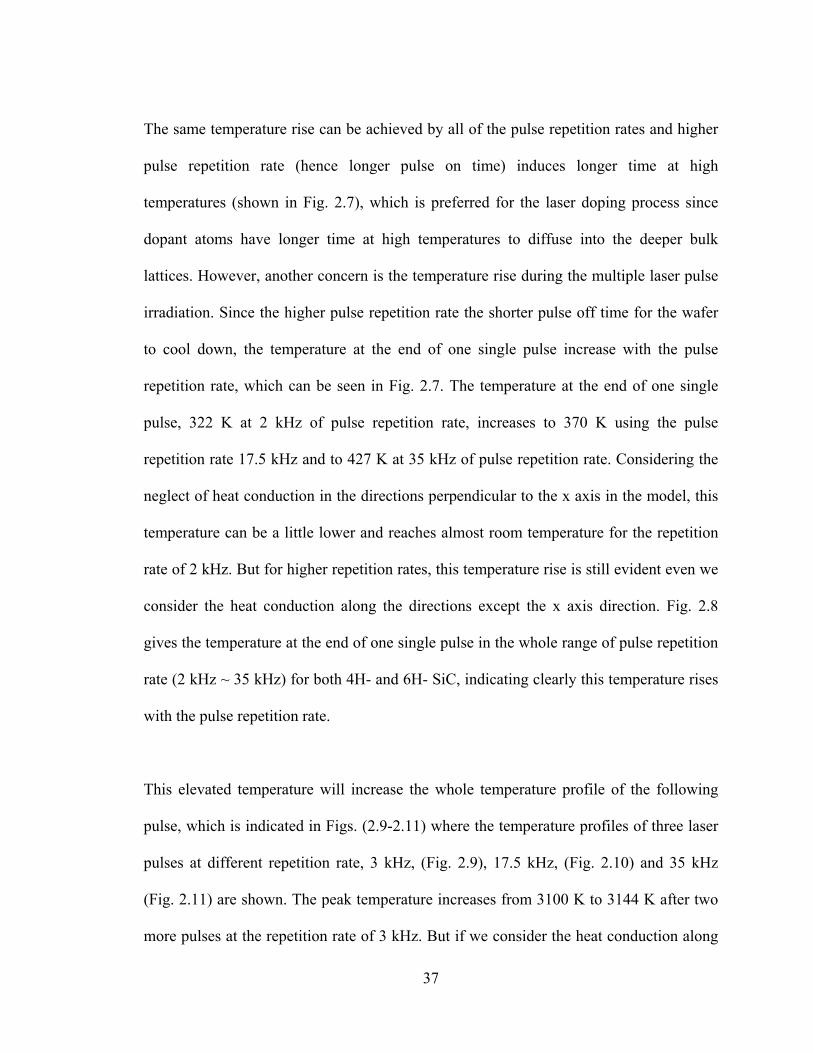
37
The same temperature rise can be achieved by all of the pulse repetition rates and higher
pulse repetition rate (hence longer pulse on time) induces longer time at high
temperatures (shown in Fig. 2.7), which is preferred for the laser doping process since
dopant atoms have longer time at high temperatures to diffuse into the deeper bulk
lattices. However, another concern is the temperature rise during the multiple laser pulse
irradiation. Since the higher pulse repetition rate the shorter pulse off time for the wafer
to cool down, the temperature at the end of one single pulse increase with the pulse
repetition rate, which can be seen in Fig. 2.7. The temperature at the end of one single
pulse, 322 K at 2 kHz of pulse repetition rate, increases to 370 K using the pulse
repetition rate 17.5 kHz and to 427 K at 35 kHz of pulse repetition rate. Considering the
neglect of heat conduction in the directions perpendicular to the x axis in the model, this
temperature can be a little lower and reaches almost room temperature for the repetition
rate of 2 kHz. But for higher repetition rates, this temperature rise is still evident even we
consider the heat conduction along the directions except the x axis direction. Fig. 2.8
gives the temperature at the end of one single pulse in the whole range of pulse repetition
rate (2 kHz ~ 35 kHz) for both 4H- and 6H- SiC, indicating clearly this temperature rises
with the pulse repetition rate.
This elevated temperature will increase the whole temperature profile of the following
pulse, which is indicated in Figs. (2.9-2.11) where the temperature profiles of three laser
pulses at different repetition rate, 3 kHz, (Fig. 2.9), 17.5 kHz, (Fig. 2.10) and 35 kHz
(Fig. 2.11) are shown. The peak temperature increases from 3100 K to 3144 K after two
more pulses at the repetition rate of 3 kHz. But if we consider the heat conduction along
38
the directions perpendicular to the x axis, as mentioned above, the temperature at the end
of the first pulse is able to reach almost room temperature, which will not affect the peak
temperature much. At the repetition rate of 17.5 kHz, the peak temperature increases
from 3100 K to 3182 K after two more pulses and this peak temperature rise is more
evident, from 3100 K to 3288 K, if 35 kHz of repetition rate is used. Such rapid peak
temperature rise will finally damage the wafer during the multiple pulse laser irradiations
so low pulse repetition rate is preferred combining all these considerations.
Fig. 2.12 gives the temperature distribution near the bottom region along the thickness of
the 6H-SiC at different transient time during one single pulse. After the bottom surface
reaches the peak temperature (curve1), heat transferred by the laser energy conducts up in
the bulk and increase the bulk temperature accompanying the decrease of surface
temperature (curves 2, 3 and 4) with the time. With the increase of distance from the
bottom surface the time that temperature reaches its peak value at that particular position
extend, shown in Fig. 2.13, such times at positions of bottom surface, 1 μm from the
surface, 2 μm from the surface and 3 μm from the surface are 48 ns, 56ns, 64 ns and 72
ns respectively.

39
0 100 200 300 400 500 80000 160000 240000 3200000
500
1000
1500
2000
2500
3000
3500
f=3 kHz f=17.5 kHz f= 35 kHz
Tem
pera
ture
(K)
Time (ns)
Figure 2.7 Temperature distribution of one single pulse with same peak temperature
(3100 K) irradiated at different pulse repetition rate (f=3, 17.5 and 35 kHz) and laser
intensity (I=88.7, 56.4 and 44.2 MW/cm2) on 6H-SiC substrate (d = 430 μm).

40
0 5 10 15 20 25 30 35 40300
320
340
360
380
400
420
440
6H-SiC 4H-SiC
Tem
pera
ture
(K)
Pulse Reperition Rate (KHz)
Figure 2.8 Variation of temperature at the end of one single pulse with pulse repetition
rate for 4H- and 6H- SiC wafers (d = 430 μm).

41
0 100 200 300 400 500 600 700 800 900 1000 11000
200
400
600
800
2600
2800
3000
3200
Tem
pera
ture
(K)
Time (μs)
Figure 2.9 Temperature profiles of three pulses of 6H-SiC wafer (d = 430 μm) irradiated
at pulse repetition rate of 3 kHz and laser intensity of 88.7 MW/cm2.

42
0 20 40 60 80 100 120 140 160 1800
200
400
600
800
2600
2800
3000
3200
Tem
pera
ture
(K)
Time (μs)
Figure 2.10 Temperature profiles of three pulses of 6H-SiC wafer (d = 430 μm) irradiated
at pulse repetition rate of 17.5 kHz and laser intensity of 56.4 MW/cm2.

43
0 20 40 60 80 1000
200
400
600
800
2600
2800
3000
3200
3400
Tem
pera
ture
(K)
Time (μs)
Figure 2.11 Temperature profiles of three pulses of 6H-SiC wafer (d = 430 μm) irradiated
at pulse repetition rate of 35 kHz and laser intensity of 44.2 MW/cm2.

44
425 426 427 428 429 430
500
1000
1500
2000
2500
3000
3500
4
3
2
1
I=91 f=3
1 t=48 ns 2 t=56 ns 3 t=64 ns 4 t=72 ns
Tem
pera
ture
(K)
Depth along the thickness of the 6H-SiC wafer (μm)
Figure 2.12 Time evolution of temperature along the thickness of the 6H-SiC wafer (d =
430 μm) near the bottom surface region. (Laser intensity: 91 MW/cm2; Pulse repetition
rate: 3 kHz).

45
0 50 100 150 200 250 3000
500
1000
1500
2000
2500
3000
3500
Time (ns)
Tem
pera
ture
(K)
bottom surface 1 μm from the surface 2 μm from the surface 3 μm from the surface 4 μm from the surface
Figure 2.13 Temperature profiles of 6H-SiC (d = 430 μm) at particular position during
the laser irradiation. (Laser intensity: 91 MW/cm2; Pulse repetition rate: 3 kHz).

46
2.3 Mathematical model and analysis of surface heating
2.3.1 Mathematical Model and Solution
The one-dimensional laser irradiation of surface heating can be described by the
following heat conduction equations, boundary conditions and initial condition.
2
2
xT
tT
αα ∂
=∂∂ (2.20)
)()( 0TTHtAIxTk −−=∂∂
− φ (2.21)
0),( TtT =∞ (2.22)
0)0,( TxT = (2.23)
In this model )(tφ defines a rectangular shape of laser pulse for excimer laser.
⎪⎩
⎪⎨⎧
=+≤<
+≤≤=
Λ2,1,0)1(0
1)(
ntntnt
tnttntt
pp
onppφ (2.24)
Take Laplace transform of Eq. (2.20) to obtain
xsxss eCeC
sT
sxT αα /2
/1
0),( ++= − (2.25)
Laplace transform of Eqs. (2.21) and (2.22) and replace into Eq. (2.23) yield
HskAI
C s
+=
αφ
/1 (2.26)
02 =C (2.27)
By using inverse Laplace transform, we obtain

47
)2
()4
exp(]/
[ 2
2
2
2/1
tx
ktHerfcee
kH
tx
tkHskeL k
tHk
Hxxs
ααα
απα
α
αα
+−−=+
−− (2.28)
)(][1 tL s φφ =− (2.29)
So T(x,t) can be expressed by using convolution theorem,
)30.2(])(2
)([
)(])(4
exp[1)(),( 2
2 )(
02
2
00
ττα
τα
τφαττατ
τφπ
α τα
dtx
ktH
erfc
eekHAId
tx
tkAITtxT k
tHtk
Hxt
−+
−
×−−
−−
+=−
∫∫
2.3.2 Results and discussion
In this case, three different lasing media of excimer laser, XeF with wavelength of
351nm, KrF with wavelength of 248 nm and ArF with wavelength of 193 nm are
considered. The absorption of the 4H- and 6H- SiC wafer used in this study at the
different wavelengths of excimer laser and their heat transfer coefficients are given in
Table 2.2.

48
Table 2.2 Absorption and heat transfer coefficients of 4H- and 6H-SiC [Levinshtein et al.
(2001)].
4H-SiC 6H-SiC
193 62 58
248 73 71
Absorption
(%) 351 77 77
Heat transfer coefficient (W/cm2K) 5 5

49
The temperature profiles of 6H- and 4H-SiC in a single pulse at three different
wavelengths and particular laser pulse intensity are shown in Figs. 2. 14 and 15,
respectively. Higher peak temperature can be reached for 4H-SiC than 6H-SiC at same
laser intensity for all the three wavelengths because of the lower thermal conductivity and
diffusivity of 4H-SiC. For both cases the wafer reaches the highest peak temperature
irradiated by the XeF with the wavelength of 351 nm and lowest peak temperature by the
ArF with the wavelength of 193 nm. However, high temperature is not the only
consideration for the laser doping process. With the decrease of the laser wavelength, the
photon energy increases. The higher photon energy the higher energy input efficiency,
which is not considered in the temperature distribution modeling. Considering both of the
temperature profile and photon energy, KrF excimer laser (λ=248 nm) is preferred
because of its much higher photon energy (5 eV) than XeF with wavelength of 351 nm
(3.53 eV) and much higher peak temperature (shown in Figs. 2.14 and 2.15) than ArF
with wavelength of 193 nm. The time evolution of temperature distribution along the
thickness of the 6H-SiC wafer irradiated by KrF laser is shown in Fig. 2.16.

50
0 50 100 150 200 250 300 350 400
500
1000
1500
2000
2500
3000
6H-SiC
λ=351nm λ=248nm λ=193nm
Tem
pera
ture
(K)
Time(ns)
Figure 2.14 Temperature profiles of 6H-SiC irradiated by different excimer laser sources
(λ=351, 248 and 193 nm) and same laser intensity (60 MW/cm2).
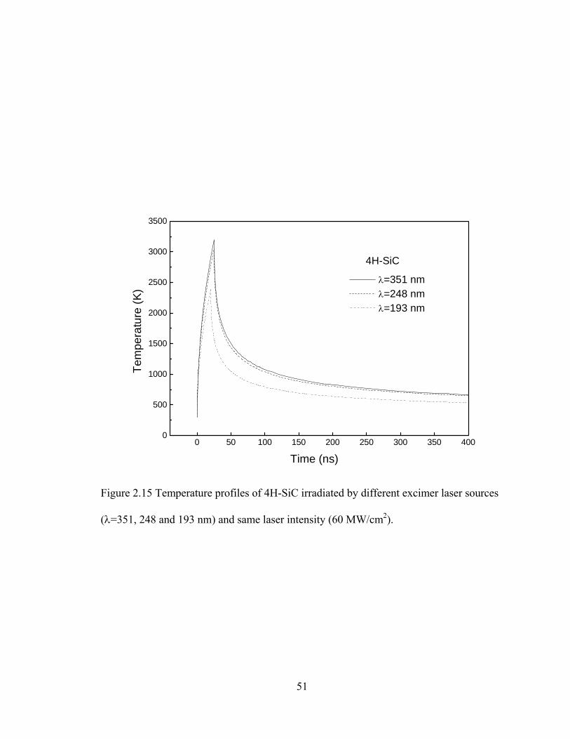
51
0 50 100 150 200 250 300 350 4000
500
1000
1500
2000
2500
3000
3500
4H-SiC
λ=351 nm λ=248 nm λ=193 nm
Tem
pera
ture
(K)
Time (ns)
Figure 2.15 Temperature profiles of 4H-SiC irradiated by different excimer laser sources
(λ=351, 248 and 193 nm) and same laser intensity (60 MW/cm2).
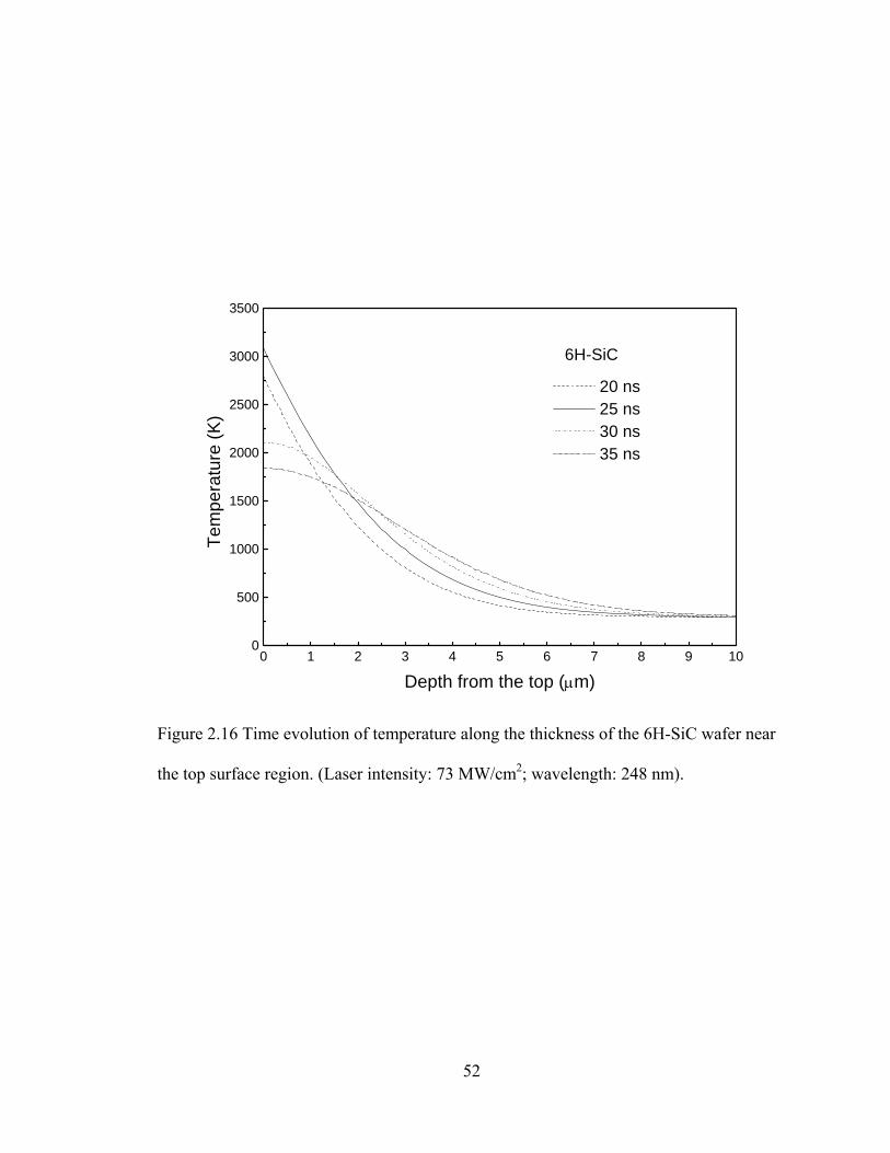
52
0 1 2 3 4 5 6 7 8 9 100
500
1000
1500
2000
2500
3000
3500
6H-SiC
20 ns 25 ns 30 ns 35 ns
Tem
pera
ture
(K)
Depth from the top (μm)
Figure 2.16 Time evolution of temperature along the thickness of the 6H-SiC wafer near
the top surface region. (Laser intensity: 73 MW/cm2; wavelength: 248 nm).
53
3 CHAPTER 3: EXPERIMENTAL METHODS AND CHARACTERIZATION TECHNIQUES
3.1 Samples Preparation
Three different silicon carbide samples purchased from II-VI incorporation were used in
this study. The corresponding characteristics of the samples are listed in Table 3.1. The
average micropipe densities of these wafers are below 12 cm-2 and the dislocation
densities are about 5.8 × 104 cm-2 [Emorhokpor et al. (2004)].
Table 3.1 Silicon carbide samples used in this study.
Sample Specifications
6H-SiC Single crystal, n-type doped with the dopant concentration of 5×10¹⁸
cm-3, 270 μm thick, one side polished
6H-SiC Single crystal, (0001) Si-face semi-insulating, 430 μm thick, one side
polished
4H-SiC Single crystal, n-type doped with 10 μm epitaxial layer with the dopant
concentration of ~1016 cm-3, 270 μm thick, epilayer side polished

54
Prior to laser irradiation experiments, all samples were first washed with soap and
deionized (D.I.) water, blow dry nitrogen gas for drying and then cleaned by soaking in
H2O2:H2SO4 solution (1:1 by volume) for 15 minutes. This was followed by rinsing with
D.I. water, dipping in buffered oxide etch (BOE), cleaning with actone, methanol and
D.I. water, and blowing dry nitrogen gas for final drying.
3.2 Laser Irradiation Experimental Set-up
Experiments can be conducted using two different laser sources: (1) A lamp-pumped
Nd:YAG laser (LEE-8150MQ) of wavelength 1064 nm that can be operated in both
continuous wave (CW) and Q-switched modes. In the CW mode, the output power of the
laser varies from 8 to 200 W. In the Q-switched mode, the pulse repetition rate and pulse
on-time can be turned in the range of 2 kHz to 35 kHz and 60 to 300 ns, respectively. The
beam profile of the Nd:YAG laser used in this study is shown in Fig. 3.1, in which the
laser beam intensity is almost uniform, and that is why we assume uniform laser beam in
the calculation of temperature distribution during laser irradiation. (2) A multigas
excimer laser (LPX 210i) with three lasing media (ArF for 193 nm wavelength, KrF for
248 nm wavelength and XeF for 351 nm wavelength). The repetition rate is in the range
of 1 to 100 Hz and the nominal pulse duration is 20 ns for wavelength of 193nm and 25
ns for wavelengths of 248nm and 351 nm.

55
(a)
(b)
Figure 3.1 Intensity profile of the incident Nd:YAG laser beam. (a) Front view. (b) Top
view.

56
A schematic of the laser doping, direct metallization and growing endolayer experimental
set-up is shown in Fig. 3.2. The sample was placed inside a vacuum chamber where it
was simultaneously irradiated with the laser beam and exposed to an appropriate gas, i.e.,
different gases for different irradiation purposes. The laser beam can focus on the top or
bottom surface of the substrate according to different heating mechanisms. The height of
the chamber can be controlled through an intermediate stage to obtain different laser spot
sizes on the SiC substrate surface. The chamber can be either stationary or moving on a
stepper motor-controlled translation stage depending on different experiment
requirements. The substrate was kept at room temperature before laser irradiation in all
the experiments.
There are three types of ambient gases used in this study:
(i) Dopant containing gas: Highly pure nitrogen gas was used as an n-type dopant source
during laser irradiation. Trimethylaluminum [(CH3)3Al (TMA)] was used as the p-type
precursor for the aluminum doping. TMA was separately heated in a bubbler until it
evaporated and then a carrier gas Ar was passed through the bubbler to deliver the TMA
vapor to the laser doping chamber through a gas-tight tube. TMA decomposes at the
laser-heated substrate surface producing Al atoms, which subsequently diffuse into the
substrate.
(ii) Inert gas such as Ar or He serving as the protecting gas during the laser direct
metallization process.
(iii) Methane (CH4): It was used as the carbon source for growing endolayer. Both the
pyrolytic and photolytic reactions during excimer laser irradiation process will contribute

57
to the formation of carbon atoms from methane for the formation of endolayers, which
will be illuminated in Chapter 6.
Figure 3.2 Experimental set-up for laser doping, direct metallization and growing
endolayer system.
Carrier Gas
Gas Tight Chamber
Soda-lime Glass Window
Motorized Translation Stage
Sample
Hot Plate
Dopant Containing Flask
Z-level Controlling Stage
Gas-Regulator and Flow meter
Bending Mirror
Focusing Lens
Exhaust
Nd:YAG Laser or Excimer Laser
Sample Holder
Motorized Translation Stage

58
3.3 Materials Characterization
Different analytical techniques were used to quantitatively determine the dopant profiles
of both n-type and p-type doped samples, study the crystal structure of the laser irradiated
samples and analysis carbon contents in the endolayer.
3.3.1 Secondary Ion Mass Spectroscopy (SIMS)
Cameca IMS-3F SIMS Ion Microscope (Second ion mass spectroscopy) was used to
determine the n-type dopant (nitrogen) and p-type dopant (aluminum) depth profiles in
the surface region of the substrates after laser doping experiments. The SIMS
measurements were performed using Cs and O2+ sources with a primary beam of ~ 8
keV. The primary beam current is 1 μA and it was rastered over an area of ~ 200×200 μm
of the laser treated wafer. The depth scale was calculated from the sputtering rate and
time.
3.3.2 Focused Ion Beam Instrument (FIB)
A FEI 200 TEM Focused Ion Beam (FIB) instrument was used to obtain 10 μm × 5 μm ×
150 nm cross-sections of the endolayer sample and parent sample in order to prepare
TEM specimens. Platinum film was deposited by Ga+ ion beam-assisted chemical vapor
deposition operating at 30 kV as a protective layer for subsequent FIB milling operation.
59
3.3.3 Transmission Electron Microscopy (TEM)
To examine the effect of laser processing on the crystalline order of the endolayer, a high
resolution transmission electron microscope, FEI Tecnai F30 TEM, operating at 200 keV
was used to study the crystal structure along the cross section of the annealed endolayer
specimen. The crystal structure along the cross section of the parent wafer was also
analyzed for comparison.
3.3.4 X-ray Energy Dispersive Spectrometry (XEDS)
To determine the thickness of the endolayer, carbon contents along the depth of both
annealed endolayer specimen and parent wafer were analyzed by line scanning on the
cross sections of both annealed endolayer specimen and parent wafer using X-ray energy
dispersive spectrometry (XEDS), equipped with FEI Tecnai F30 TEM.
3.3.5 Rutherford Backscattering Spectroscopy (RBS)
Geneal IONIX 1.7MU Tandetron RBS system, involving the channeling of a 1.4 MeV He
beam, was used to analyze the lattice disorder of laser induced solid phase diffusion
processed specimens by comparing their aligned RBS channeling spectra with that of the
parent wafer.

60
3.4 Electrical Characterization
3.4.1 Current-Voltage (I-V) Characteristics of the Laser Direct Metallized Electrodes
The contact between the substrate and the electrode has a rectifying or ohmic property
that can be indicated by different I-V characteristics of the electrodes on the substrate.
Current-Voltage measurements between two separated laser direct metallized electrodes
on the SiC substrate were performed using a Tektronix 576 curve tracer by contacting the
electrodes directly with microprobes.
3.4.2 Resistivity of the Endolayer
The resistivity of the endolayer is calculated using the expression [Edwards, et al.
(1997)], ρ = RA/d, where A is the area of the top Ni contact, d is the thickness and R is
the resistance of the endolayer. To obtain the resistance of the endolayer, I-V
characteristics of the endolayer sample and the parent wafer were analyzed. The
resistance of the endolayer sample (R) obtained from I-V measurements are the sum of
the resistances of the endolayer (Re), contacts (Rc) and substrate (Rs) [Nadella and
Capano (1997)]. Knowing R and the sum of the resistances of the contact and substrate
obtained from the parent sample, the resistance of endolayer is obtained. The resistivities
of both the as-formed endolayer and annealed endolayer are obtained using this method.

61
3.4.3 Current-Voltage (I-V) Characteristics of the PIN Diodes
Forward and reverse Current-Voltage (I-V) measurements of laser fabricated PIN diodes
on different mediums, including laser fabricated endolayer and as-received homoepilayer,
were performed by using a Tektronix 576 curve tracer by contacting the metal deposits or
laser direct metallized electrode with microprobes. Breakdown voltage and Forward
Voltage drop at 100A/cm2 of the diodes are indicated from their I-V characteristics.
3.5 Optical Characterization
3.5.1 Laser Beam Characteristics
A laser beam analyzer, Spiricon LBA 300 PC, connected to a pyroelectric camera
(Pyrocam I) was utilized to measure the Nd YAG laser beam profile. A highly reflective
mirror was put in the optical path between the output laser beam and the camera to avoid
the damage of camera detector, whose damage threshold is 4 W/cm2.
3.5.2 Reflectivity and Transmitivity of Optical Structure at Particular Wavelength
The optical properties (reflectivity and transmission) of the parent 6H-SiC wafer and the
laser synthesized embedded structures were calculated based on the transmitted (PT) and
reflected (PR) powers measured at a laser wavelength of 1064 nm, whose set-up will be
illuminated in Chapter 6.

62
4 CHAPTER 4: LASER DOPING AND DIRECT METALLIZATION OF SILICON CARBIDE
4.1 Introduction
Lasers have been used to incorporate dopants into semiconductor wafers and such
techniques have been classified as laser thermal processing (LTP), gas immersion laser
doping (GILD) and laser-induced solid-phase doping (LISPD) as we reviewed in Chapter
1. Lasers also have been utilized in several methods to form ohmic contacts or improve
the performance of ohmic contacts to SiC in the literatures. Pulsed laser deposition (PLD)
of Ni2Si on 4H n-type SiC was conducted by excimer laser at room temperature and
followed by rapid thermally annealing (RTA) for 30s at 950°C, which resulted in very
good ohmic behavior [Cole, M. W. et al. (2001). Pulsed laser doping (PLD) method was
used to in-situ dope Ni impurities to form ohmic electrodes in SiC, in which Ni impurities
were provided by Ni vapor that continuously evaporated to the SiC substrate using the
thermal evaporation source within the vacuum chamber [Eryu et al. (1997)].
Laser dopant incorporations on different semiconductors (SiC and GaN) have been
conducted in our group using different doping techniques [Salama (2003)]. However,
more work need to be done in this section such as doping mechanisms and effective
diffusivity analysis of dopants. This chapter presents experimental results on n-type and
p-type laser doping of different SiC polytypes using different laser sources and laser

63
doping methods and the discussion of the laser doping mechanisms and effective
diffusivity of the dopants.
Laser direct metallization on n-type SiC based on the laser direct write technique in our
group has been illuminated in the previous work, in which laser induced conversion of
electric resistivity, surface analysis of the laser metallized SiC, Schottky barrier height
calculation of laser fabricated rectifying contacts and specific contact resistance
calculation of laser fabricated ohmic contacts were discussed [Salama (2003)]. This
method relies on the ability of laser to locally change the stoichiometry of the SiC in the
laser-treated region through the photonic and thermal energy coupling between the beam
and the material by transforming SiC surface into either Si-rich (excimer laser irradiation)
or C-rich phases (Nd:YAG laser irradiation) [Salama (2003)]. In this chapter this method
was extended by combining the laser direct metallization with the laser doping to
improve the performance of the contact, i.e., fabrication of laser direct metallized contact
on heavily laser doped SiC substrate.
4.2 Laser Doping Process of Silicon Carbide
Two different methods, illuminated in section 2.1, are used to dope silicon carbide. The
laser irradiation parameters are listed in Table 4.1. For internal heating method, in which
Nd:YAG laser with the wavelength of 1064 nm is used, low pulse repetition rates (3 kHz)
are chosen because of the consideration of temperature rise during the multiple pulse

64
laser irradiation. For surface heating method, KrF excimer laser with the wavelength of
248 nm rather than ArF excimer laser (λ = 193 nm) and XeF excimer laser (λ= 351 nm)
is chosen because of the high absorption of silicon carbide with respect of the wavelength
of 248 nm and the high photo energy of the laser light with 248 nm wavelength.
Fig. 4.1 shows the temperature distribution of 6H-SiC during n-type doping using the
parameters of laser internal heating listed in Table 4.1. The peak temperature of the
bottom surface, where is the location of highest temperature during the laser irradiation
shown in Fig. 2.2, is below the decomposition temperature of silicon carbide (Fig. 4.1a).
That means the wafer does not melt during the laser doping process. This will allow
fabrication of electronic devices using the doped sample. The transient temperature
distribution along the thickness of the wafer from the bottom surface at the peak
temperature (t=48ns) (Fig. 4.1b) shows the non-uniformly temperature distribution
decreasing along the substrate thickness from the bottom surface.

65
Table 4.1 Processing parameters for different laser doping methods.
Methods Internal Heating Surface Heating
Sample n-type 6H-SiC n-type 6H-SiC n-type 4H-SiC with epilayer
Doped region n-type p-type p-type
Laser source Nd:YAG Nd:YAG KrF excimer
Wavelength (nm) 1064 1064 248
Pulse repetition rate (Hz)
3000 3000 1
Beam area (cm2) π(0.03)2/4 π(0.03)2/4 0.2×0.4
Pulse energy (mJ)
4 4.33 120
Laser fluence (J/cm2)
5.65 6.1 1.5
Pulse intensity (MW/cm2)
78.6 85.1 60
Scanning speed (mm/s)
1 1 -
Irradiation passes 1 1 -
Laser shots - - 1000, 3000
Ambient gas N2 at 30 psi TMA delivered by Ar at 30 psi
TMA delivered by Ar at 30 psi

66
0 20 40 60 80 100 120 140 160 180 2000
400
800
1200
1600
2000
2400
2800
3200
Tem
pera
ture
(K)
Time (ns)
3100 K
(a)
268.0 268.2 268.4 268.6 268.8 269.0 269.2 269.4 269.6 269.8 270.01000
1200
1400
1600
1800
2000
2200
2400
2600
2800
3000
3200
3400
Tem
pera
ture
(K)
Depth along the thickness of the wafer (μm)
3100K
(b)
Figure 4.1 Temperature distribution of 6H-SiC during n-type doping using the parameters
of method A listed in Table 4.1.(a) Bottom surface temperature distribution with the time;
(b) Transient temperature distribution along the thickness of the wafer from the bottom
surface at the peak temperature (t=48ns).

67
Fig. 4.2 shows the temperature distribution of 6H-SiC during p-type doping using the
internal heating method listed in Table 4.1. Different from n-type doping in which the
absorption of laser energy by the dopant, nitrogen gas, is negligible, during p-type
doping, certain amount of laser energy will be absorbed by the chamber window because
of the deposition of aluminum on it and the high concentration dopant, trimethyaluminum
(TMA) itself. The amount of laser energy absorbed by the window and dopant depends
on the dopant concentration, wavelength of the laser, laser beam area, and the distance
laser light passing through in the dopant ambient. In this case the loss of laser energy
about 10% is estimated and hence the peak temperature is around 3000 K. Such
estimation is based on the experiment phenomenon that decomposition of silicon carbide
is observed if the pulse energy is increased from 4.33 mJ to 4.6 mJ, which corresponds to
peak temperature slightly above peritectic temperature (3125 K) when considering 10%
loss of laser energy by the medium. The transient temperature distribution along the
thickness of the wafer from the bottom surface at the peak temperature (t=48ns) (Fig.
4.2b) also shows the non-uniformly temperature distribution decreasing along the
substrate thickness from the bottom surface.

68
0 20 40 60 80 100 120 140 160 180 2000
400
800
1200
1600
2000
2400
2800
3200
3600
Withour loss in the ambient 10% loss of laser energy due to the ambient
Tem
pera
ture
(K)
Time (ns)
3100 K
(a)
268.0 268.2 268.4 268.6 268.8 269.0 269.2 269.4 269.6 269.8 270.01000
1200
1400
1600
1800
2000
2200
2400
2600
2800
3000
3200
3400
Tem
pera
ture
(K)
Depth along the thickness of the wafer (μm)
3100K
(b)
Figure 4.2 Temperature distribution of 6H-SiC during p-type doping using the parameters
of method A listed in Table 4.1.(a) Bottom surface temperature distribution with the time;
(b) Transient temperature distribution along the thickness of the wafer from the bottom
surface at the peak temperature (t=48ns).
69
The temperature distribution of 4H-SiC during p-type doping using the parameters of
surface heating listed in Table 4.1 is shown in Fig.4.3. The loss of laser energy is
estimated as about 5% considering the lower Trimethylaluminum concentration filled in
the chamber compared to the former case and the experimental observation that the wafer
was decomposed by increasing the pulse energy from 120 mJ to 130 mJ, which
corresponds to peak temperature slightly above peritectic temperature (3130K) when
considering 5% loss of laser energy by the medium. The transient temperature
distribution along the thickness of the wafer from the top surface at the peak temperature
(t=25ns) (Fig. 4.3b) shows the non-uniformly temperature distribution decreasing along
the substrate thickness from the top surface.
The temperature profile in Fig. 4.3a is much narrower than in Figs. 4.1a and 4.2a. This
indicates that the sample remains at high temperature for much shorter time during
excimer laser irradiation than during Nd:YAG laser irradiation at similar peak
temperature. Therefore the dopant atoms will have much shorter time to diffuse into the
substrate during excimer laser doping than during Nd:YAG laser doping.

70
0 20 40 60 80 100 120 140 160 180 2000
400
800
1200
1600
2000
2400
2800
3200
3600
Withour loss in the ambient 5% loss of laser energy due to the ambient
Tem
pera
ture
(K)
Time (ns)
3100 K
(a)
0.0 0.2 0.4 0.6 0.8 1.0 1.2 1.4 1.6 1.8 2.01000
1200
1400
1600
1800
2000
2200
2400
2600
2800
3000
3200
3400
Tem
pera
ture
(K)
Depth along the thickness of the wafer (μm)
3100 K
(b)
Figure 4.3 Temperature distribution of 4H-SiC during p-type doping using the parameters
of method C listed in Table 4.1.(a) Top surface temperature distribution with the time; (b)
Transient temperature distribution along the thickness of the wafer from the top surface at
the peak temperature (t=25ns).
71
4.3 Doping profiles
Dopant depth profiles of laser doped wafers were obtained using secondary ion mass
spectroscopy (SIMS). Before the SIMS measurements aluminum surface residue was
removed by immersing the sample in a KOH solution for several minutes. KOH attacks
aluminum aggressively but etches SiC very slowly. Then the sample was rinsed with D. I.
water and blown nitrogen gas for drying.
4.3.1 Doping Profiles Obtained by Laser Internal Heating
Fig. 4.4 shows n-type nitrogen dopant concentration along the depth of 6H-SiC wafer,
which was obtained by the Nd:YAG laser doping process. The results indicate that the
nitrogen concentration at the wafer surface, approximately 1×1021 cm-3, drops to the
background nitrogen concentration of about 1.5×1019 cm-3 within a depth of
approximately 800 nm. It should be noted that the surface concentration of nitrogen
(1×1021 cm-3) exceeds its maximum solubility limit in 6H-SiC (6×1020 cm-3 [Schöner
(2002)]), which can be explained by the non-equilibrium process of laser doping in
silicon carbide because of high cooling rate due to the excellent thermal conductivity of
silicon carbide. Fig. 4.5 shows the p-type aluminum dopant concentration along the depth
of 6H-SiC wafer, obtained using the same Nd:YAG laser doping process as for nitrogen
doping. The aluminum concentration at the wafer surface is approximately 5×1020 cm-3,
which drops to about 1.5×1018 cm-3, the background of aluminum in the near surface
region, at a depth of about 800 nm.

72
The neat dopant concentration profiles of nitrogen and aluminum after removing the
background concentration are compared in Fig. 4.6. The two profiles show similar
decreasing curves, indicating their similar diffusion mechanisms. In both of the profiles
there are two diffusion regions can be identified according to the evident change of the
profile slopes. The first region is located near the surface, within the depth of
approximately 200 nm for nitrogen and about 100 nm for aluminum, corresponding to the
fast decrease of the dopant concentration (large curve slope) in the whole profiles. In this
region the slope of the aluminum dopant profile is larger than that of nitrogen, indicating
that aluminum atoms diffuse slower than that of nitrogen. The rest part of the profiles can
be considered as the second diffusion region, with the characteristic of relatively smaller
curve slope compared with the first region. The change of the curve slope indicates the
change of the diffusion mechanisms.

73
0 100 200 300 400 500 600 700 800 900 1000
1019
1020
1021
Nitr
ogen
dop
ant c
once
ntra
tion
(cm
-3)
Depth of the SiC wafer (nm)
1 Background (Ca)2 Nitrogen dopant profile (Cd)
12
Figure 4.4 Nitrogen dopant profiles obtained with a Nd:YAG laser. Ca: Concentration of
nitrogen in the as-received wafer; Cd: Concentration of nitrogen in the doped wafer.

74
0 100 200 300 400 500 600 700 800 900 1000
1018
1019
1020
Alu
min
um d
opan
t con
cent
ratio
n (c
m-3)
Depth of the SiC wafer (nm)
1 Background2 Aluminum dopant profile
12
Figure 4.5 Concentration depth profiles of aluminum doped by LISPD method measured
with SIMS.
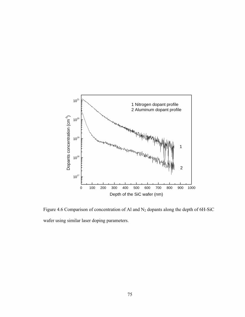
75
0 100 200 300 400 500 600 700 800 900 1000
1017
1018
1019
1020
1021
Dop
ants
con
cent
ratio
n (c
m-3)
Depth of the SiC wafer (nm)
1 Nitrogen dopant profile2 Aluminum dopant profile
1
2
Figure 4.6 Comparison of concentration of Al and N2 dopants along the depth of 6H-SiC
wafer using similar laser doping parameters.

76
4.3.2 Doping profiles obtained by Laser Surface Heating
Fig. 4.7 shows aluminum dopant concentration distribution, which was obtained with the
KrF excimer laser doping process. The substrate was doped to a depth of 200 nm with
maximum dopant concentration 2 × 10²² atoms/cm3 using 1000 laser pulses in the doping
experiment. 3000 laser pulses drove the dopant to a depth of about 450 nm. The junction
depth of 200 nm obtained here is much higher than that in the ref [Eryu et. Al (1995)]
where 50 nm junction depth was obtained on 6H-SiC using same parameters by KrF
excimer laser with the wavelength of 248 nm. The changes in the slopes of the
concentration profiles at the depth of about 120 -150 nm indicate fast and slow diffusion
processes in the near-surface and far-surface regions respectively.

77
0 50 100 150 200 250 300 350 400 450 500 550 600
1016
1017
1018
1019
1020
1021
1022
1023
3
2
1
Alu
min
um d
opan
t con
cent
ratio
n (c
m-3)
Depth of the SiC wafer (nm)
1 Background (Ca)2 1000 laser pulses (Cd1)3 3000 laser pulses (Cd2)
Figure 4.7 Aluminum dopant profiles obtained with an excimer laser. Ca: Concentration
of aluminum in the as-received wafer; Cd1: Concentration of aluminum in the 1000 laser
pulses doped wafer; Cd2: Concentration of aluminum in the 3000 laser pulses doped
wafer.

78
4.4 Mechanisms of Laser Doping Process
The dopant atoms pass through a non-uniformly heated region with a maximum
temperature at the surface region and decreasing along the substrate thickness. This
lowers the thermal energy of the diffusing atoms as they travel along the substrate
thickness and therefore their diffusion is controlled by the less energetic processes such
as interstitial diffusion. The diffusion coefficient is generally given by
[ ])Tk/(QexpDD B0 −= (4.1)
where D0 is the mass diffusivity, Q activation energy, kB Boltzmann constant and T the
absolute temperature of the substrate. Q/(kBT) represents the ratio of the activation
energy of the diffusion process to the thermal energy (kBT) at a given temperature. For
symmetric lattice structures, interstitial diffusion has lower activation energy (Q=0.5-1.5
eV) than substitutional diffusion (Q = 3-5 eV) [Pankove (1999)] since no energy is
required to form a vacancy in interstitial diffusion. So the dopant atoms possessing higher
thermal energy near the wafer surface have the ability to diffuse by more than one
mechanism, such as substitutional and interstitial mechanisms, simultaneously. As the
diffusion depth increases, the diffusion mechanism changes depending on the specifics of
the laser-induced temperature field and the diffusivity is expected to decrease [Salama
(2003)].
The diffusion of dopant atoms into the bulk silicon carbide can be explained by
considering the laser-enhanced substitutional and interstitial diffusion mechanisms.
Laser-induced heating and stresses can generate defects such as vacancies, which are
79
normally localized near the solid surface. The concentration of vacancies can be very
high in semiconductors up to 1019 or 1020 cm-3 near their melting temperature. The
vacancy concentration can be much higher than their equilibrium values due to thermal
diffusion, stress effects related to thermal expansion, laser-induced shock waves and
electronic or vibrational excitations [Bäuerle (2000)]. So in the near-surface region, the
dopant atoms can easily diffuse into the bulk by occupying these vacancies as well as
interstitial sites because of the low activation energy for interstitial diffusion. The site
occupancy can be analyzed by using the following relationships because it has been
found that Al preferentially occupies Si vacancy sites [Gadiyak (1998)] and N
preferentially occupies C vacancy sites in SiC:
Ni + VC = NC (4.2)
Ali + VSi = AlSi (4.3)
where Ni and Ali represent the nitrogen and aluminum atoms at the interstitial sites
respectively, VC and VSi denote carbon and silicon vacancies respectively, NC represents
nitrogen occupying the lattice site of carbon, and AlSi represents aluminum occupying the
lattice site of silicon. The substitutional impurities, however, have a low probability of
diffusing substitutionally, while the interstitial impurities have a much higher diffusion
coefficient since they are less strongly bound to the lattice. The diffusion process is then
dominated by the highly mobile interstitials [Schubert (1993)] in the far-surface region.

80
4.5 Effective Diffusivity Analysis
Usually the diffusivities of dopants, such as aluminum, in silicon carbide are very low
both from vapor source and ion implantation because of the chemical inertness and
densely packed atomic structure of silicon carbide. The diffusion coefficient of aluminum
in SiC is 2×10-15 cm2/s at a temperature of 1700°C [Usov (1999a)] and 3×10-14 - 6×10-12
cm2/s at temperatures higher than 2500°C from typical vapor sources [Schöner (2002)],
and 2.7×10⁻¹⁴ cm2/s during 1800°C annealing after ion implantation at room temperature
[Tajima (1982)]. It has been reported that the diffusion of aluminum can be enhanced in
silicon carbide during ion implantation at high temperatures [Suvorov (1996), Usov
(1999a) and Usov (1999b)]. Usov et al [1999a] implanted aluminum into 6H-SiC wafers
at 1700°C, showing the widening of the dopant concentration profile in the near-surface
region and the anomalous deep penetration tail compared with the Gaussian distribution
of the aluminum profiles of the sample implanted at room temperature. They reported
diffusivities in the range of 1.5×10⁻¹²- 2×10-14 cm2/s and 5×10-11- 2×10-12 cm2/s in the
near-surface and far-surface regions respectively, and the diffusivities in both regions
decrease with the increase in the implantation time. Their data also shows that the
diffusivity is lower in the near-surface region than in the far-surface region.
The driving forces for the diffusion of dopants in silicon carbide differ between the laser
doping and high temperature ion implantation methods. During ion implantation, the
substrate is kept at a constant temperature and the diffusion of aluminum is enhanced by
the vacancies and interstitials generated by the bombarding ions; so the diffusion occurs

81
under an isothermal condition. During laser doping, however, the substrate experiences
both temporal and spatial variation of temperature (Figs. 3-6); so the diffusion occurs
under a non-isothermal condition. Therefore, the variation of the diffusion coefficient as a
function of temperature, D(T), needs to be considered to understand the laser doping
process. The temperature dependence of D(T) can be approximated by
)),(
exp()( 0 tzTTDTD A−= ∗ . (4.4)
Here ∗0D is the pre-exponential factor, T(z,t) is the absolute temperature of the substrate
and TA is the activation temperature for the diffusion process, which is defined as
TA = Q/kB (4.5)
where Q is the activation energy and kB is the Boltzmann constant.
For symmetric lattice structures, interstitial diffusion has a lower activation energy
(Q=0.5-1.5eV) than substitutional diffusion (Q=3-5eV) [Pankove, (1999)] since no
energy is required to form a vacancy in interstitial diffusion. So the dopant atoms
possessing higher thermal energy near the wafer surface could be capable of diffusing by
more than one mechanism, such as substitutional and interstitial mechanisms,
simultaneously. As the diffusion depth increases, the diffusion mechanism changes
depending on the specifics of the laser-induced temperature field and the diffusivity is
expected to decrease. Based on the available data [Neudeck et al. (2000) and
Ruschenschmidt et al. (2001)] for the diffusion coefficients of N2 and Al in SiC in the
temperature range of 1800°C - 2450°C, the values of Q are calculated to be 2.25 eV for

82
nitrogen and 3.40 eV for aluminum and the values of ∗0D are found to be 5.8 × 10⁻⁸ cm2/s
and 5.9 × 10⁻⁶ cm2/s for N2 and Al respectively by using Eq. (4.4).
Since the peritectic reaction temperature for SiC is ~ 2800 °C, the dopant diffusion
temperature T(z, t) will be less than the peritectic temperature for laser doping of SiC
without melting the wafer. However the activation temperatures (TA = Q/kB) are 2.6 × 10⁴
K and 3.9 × 10⁴ K for nitrogen and aluminum, respectively, which are much larger than
T(z, t). So the ratio TA/T(z,t) is very large. This fact will be utilized later in this section to
determine the mass diffusion length.
The one-dimensional dopant diffusion process can be represented by [Libenson et al.
(1973)]
)),()),(((),(z
tzCtzTDzt
tzC∂
∂∂∂
=∂
∂ z ≥ 0, t > 0 (4.6)
C(z,0)=0 z > 0 (4.7a)
C(0,t) = C0 t > 0 (4.7b)
C(∞,0)=0 t > 0 (4.7c)
The thermal diffusivity of 6H-SiC is 2.2 cm2/s, which is much higher than the mass
diffusivity of various dopants in SiC (Table 4.2). Therefore, the thermal diffusion length
is expected to be much deeper than the mass diffusion length. So the temperature can be
considered to be uniform over the small mass diffusion length and then Eq. (4.6) can be

83
solved by considering )),(( tzTD to be a function of the substrate surface temperature,
i.e., )).,0(()),(( tTDtzTD = (4.8)
So Eq. (4.6) can be rewritten as
2
2 ),()),0((),(z
tzCtTDt
tzC∂
∂=
∂∂ (4.9)
To solve Eq. (4.9) a new variable η is defined such that
∫ ′′=t
tdtTD0
)),0((η (4.10)
Then we can get
),(),( ηzCtzC ′≡ (4.11)
or ηη
dcdzzcdt
tcdz
zc
∂′∂
+∂′∂
≡∂∂
+∂∂ (4.12)
This yields
zc
zc
∂′∂
=∂∂ (4.13)
and ηη
dcdttc
∂′∂
=∂∂ (4.14)
or )),0(( tTDcdtdc
tc
ηη
η ∂′∂
=∂′∂
=∂∂ (4.15)
Then considering Eq. (4.9), (4.11) and (4.15) together, Eq. (4.16) can be obtained
2
2 ),(),(z
zCzC∂′∂
=∂′∂ ηηη (4.16)
The solution to Eq. (4.16) yields the following expression for the dopant concentration
distribution:
84
)(),( 0mlzerfcCzC =′ η , (4.17)
satisfying the initial and boundary conditions (4.7a-c). It should be noted that Eq. (4.17)
is based on the assumption that the host lattice contains no dopant atoms prior to the
onset of the diffusion process and therefore it is suitable only for a single irradiation pass.
The mass diffusion length ml in Eq. (4.17) is given by
∫ ′′≈t
m tdtTDl0
)),0((2 (4.18)
Now ∫∫ ′=′′ ′−t tT
Tt
tdeDtdtTDA
0
),0(00
)),0(( (4.19)
Generally TA >> T(0,t’). We define
),0( tT ′=θ (4.20)
then tdt
tTd ′′∂′∂
=),0(θ (4.21)
or ),0( tT
dtd′
=′ &θ (4.22)
So Eq. (4.19) can be rewritten as
∫∫ ′=′′
−).0(
000 ),0()),0((
tT
T
td
tTeDtTDtd
A
θθ
& (4.23)
and this equation can be approximated by
∫∫−
∂∂
≈′′),0(
0
0
0 ).0()),0((
tTT
tde
ttT
DtTDtd
A
θθ
),0(0
2
),0(),0( tT
T
A
A
eDtTTtT −
≈ &
85
)),0((),0(),0(2
tTDtTTtT
A&= (4.24)
the surface temperature is
πα
ktItT 2),0( = (4.25)
and tk
ItTπα
=),0(& (4.26)
then
tkIk
tI
tTtTtT
παπα2
),0(),0(),0(2
=&
ttT ),0(2= (4.27)
So the integral in Eq.(4.18) can be approximated as [Libenson et al. (1973)]
A
t
TttTDtTtTDtd )),0((),0(2)),0((
0≈′′∫ (4.28)
Eq. (4.18) and Eq. (4.28) yield
Am T
tTtDtTl ))((),0(22= (4.29)
or t)t,0(T8
T))t,0(T(D A
2ml= (4.30)
or t
ktI
TltTD A
2m
πα28
)),0((×
=
23
2
16 tCkI
Tl
p
Am
×××=
ρπ
(4.31)

86
Now C(z, t) can be expressed as
⎟⎟⎟⎟⎟
⎠
⎞
⎜⎜⎜⎜⎜
⎝
⎛
=
BkQtTtDtT
zerfcCtzC
/))((),0(22
),( 0 (4.32)
For the near-surface region the diffusion time t is taken as 20% and 10% of the total
laser-wafer interaction time for Nd:YAG and excimer lasers, respectively. These
percentages approximately correspond to the high temperature (~3000 K) heating time
during which the vacancies are expected to form in high concentrations at the near-
surface region [Bäuerle (2000)], leading to high diffusivity. A higher percentage is
chosen for Nd:YAG laser doping because the substrate remains at higher temperatures for
longer times than in the case of excimer laser doping as discussed in Section 4.2. The
total laser-wafer interaction time is given by Prtirrton, where Pr is the pulse repetition rate,
tirr is the total laser irradiation time (pulse-on plus pulse-off times), ton is the pulse length
(pulse-on time). tirr is given by 2r0/v in the case of a scanning beam, where r0 is the radius
of the laser beam on the wafer surface and v is the laser scanning speed.
The calculated concentration profile C(z, t) matches with the nitrogen dopant profile (Fig.
4.8a, Nd:YAG laser doping process) at the near-surface region within 160 nm very well
for t = 13 μs, T(0,t) ≈ 3000 K and D(T(t)) ≈ 2.4 × 10⁻⁵ cm2/s, validating the
approximation D(T(z,t)) ≈ D(T(0,t)). For the case of excimer laser doping, the calculated
concentration profiles C(z,t) for both 1000 and 3000 laser pulses also match well with the
experimental aluminum dopant profile (Fig. 4.9a) at the near-surface region over a depth

87
of 120 nm for 1000 pulses and 150 nm for 3000 pulses for t = 2.5 and 7.5 μs for 1000 and
3000 laser pulses, respectively, T(0,t) ≈ 3000 K and D(T(t)) ≈ 1.2 × 10⁻⁵ cm2/s for both
pulses.
However, the theoretical dopant profile deviates from the experimental data at the far-
surface region because the temperature there is significantly different from the substrate
surface temperature, T(0,t) and, therefore, the above approximation is invalid in the far-
surface region. Additionally different diffusion mechanisms dominate in the near-surface
and far-surface regions. At the near-surface region the dopant atoms can diffuse by
occupying vacancies created by laser irradiation, and interstitial sites. The effect of lasers
on the creation of vacancies generally diminishes as the distance from the hottest point
increases. So the diffusion mechanism gradually changes with distance and ultimately it
is dominated by the interstitial mechanism in the far-surface region. So the theoretical
dopant profile, Eq. (4.32), can be modified as follows by considering another effective
diffusion coefficient, which denotes the diffusion behavior in the far-surface region.
⎟⎟
⎠
⎞
⎜⎜
⎝
⎛
′+
⎟⎟⎟⎟⎟
⎠
⎞
⎜⎜⎜⎜⎜
⎝
⎛
=tD
zerfcC
kQtTtDtT
zerfcCtzCfs
B
2/
))((),0(22),( 10 (4.33)
Here C1 is a characteristic concentration representing the diffusion process in the far-
surface region, Dfs denotes the average diffusion coefficient in the far-surface region and
t ′ is the diffusion time in the far-surface region, which is taken as the total laser-wafer
interaction time for the Nd:YAG and excimer lasers respectively. The values of t, t ′ , C0,

88
C1, Q and kB are listed in Table 4.2 for both Nd:YAG and Excimer laser doping
experiments. The modified profile, Eq. (4.33), fits the experimental dopant profile quite
well as shown in Fig. 4.8b (Nd:YAG laser doping) for C1 = 1.4×1020 cm-3, Dfs = 9.2×10⁻⁶
cm-3 and t ′ = 65 μs. For the case of excimer laser doping the modified profiles also fit
well with the experimental dopant profiles as shown in Fig. 4.9b for C1 = 1×1019 cm-3, t ′
= 25 μs and Dfs = 1.3×10⁻⁶ cm-3 in the case of 1000 laser pulses, and C1 = 1.7×1020 cm-3,
t ′ = 75 μs and Dfs = 1.3×10⁻⁶ cm-3 in the case of 3000 laser pulses.
Two sets of diffusion coefficients are obtained for each laser doping process and these
values are listed in Table 4.3. Similar enhancement in the dopant diffusion coefficient has
been reported for laser doping in Si [Kimerling (1980)] as listed in the table. The mass
diffusivities of nitrogen are 2.4 × 10⁻⁵ cm2/s for near-surface region and 9.2 × 10⁻⁶ cm2/s
for far-surface region. The corresponding results of aluminum are 1.2 × 10⁻⁵ cm2/s for
near-surface region and 1.3 × 10⁻⁶ cm2/s for far-surface region. These values are 6 order
of magnitude higher than the typical values of 5×10-12 cm2/s for nitrogen and 3×10-14 -
6×10-12 cm2/s for aluminum [Schöner (2002)], indicating that lasers enhance the dopant
diffusion in silicon carbide significantly.
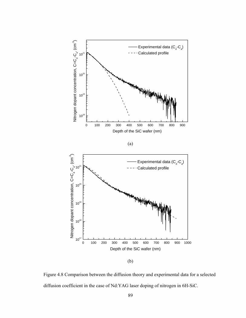
89
0 100 200 300 400 500 600 700 800 900
1018
1019
1020
1021
Nitr
ogen
dop
ant c
once
ntra
tion,
C=C
d-Ca, (
cm-3)
Depth of the SiC wafer (nm)
Experimental data (Cd-Ca) Calculated profile
(a)
0 100 200 300 400 500 600 700 800 900 10001017
1018
1019
1020
1021
Nitr
ogen
dop
ant c
once
ntra
tion,
C=C
d-Ca, (
cm-3)
Depth of the SiC wafer (nm)
Experimental data (Cd-Ca) Calculated profile
(b)
Figure 4.8 Comparison between the diffusion theory and experimental data for a selected
diffusion coefficient in the case of Nd:YAG laser doping of nitrogen in 6H-SiC.

90
0 100 200 300 400 500 6001016
1017
1018
1019
1020
1021
1022
1023
Alum
inum
dop
ant c
once
ntra
tion,
C=C
d-Ca, (
cm-3)
Depth of the SiC wafer (nm)
Experimental data for 1000 pulses (Cd1-Ca) Calculated profile for 1000 pulses Experimental data for 3000 pulses (Cd2-Ca) Calculated profile for 3000 pulses
(a)
0 100 200 300 400 500 6001016
1017
1018
1019
1020
1021
1022
1023
Experimental data for 1000 pulses (Cd1-Ca) Calculated profile for 1000 pulses Experimental data for 3000 pulses (Cd2-Ca) Calculated profile for 3000 pulses
Alu
min
um d
opan
t con
cent
ratio
n, C
=Cd-C
a, (cm
-3)
Depth of the SiC wafer (nm)
(b)
Figure 4.9 Comparison between the diffusion theory and experimental data for a selected
diffusion coefficient in the case of KrF excimer laser doping of aluminum in 4H-SiC.

91
Table 4.2 Fitting parameters used in Eqs. 4.32 and 4.33 to compare the theory with
experimental dopant profiles in Figs. 4.8 and 4.9 for determining the effective diffusivity.
Calculated curve
Fig. 4.8a Fig. 4.8b Fig. 4.9a, 1000
pulses
Fig. 4.9b, 1000
pulses
Fig. 4.9a, 3000
pulses
Fig. 4.9b, 3000 pulses
C0 (cm-3) 1.2×10²¹ 1.2×10²¹ 2.5×10²² 2.5×10²² 2.5×10²² 2.5×10²²
t (s) 1.3×10⁻⁵ 1.3×10⁻⁵ 2.5×10⁻⁶ 2.5×10⁻⁶ 7.5×10⁻⁶ 7.5×10⁻⁶
t ′ (s) - 6.5×10⁻⁵ - 2.5×10⁻⁵ - 7.5×10⁻⁵
T(0,t) (K) ~3000 ~3000 ~3000 ~3000 ~3000 ~3000
Dnear-surface (cm2/s)
2.4×10⁻⁵ 2.4×10⁻⁵ 1.2×10⁻⁵ 1.2×10⁻⁵ 1.2×10⁻⁵ 1.2×10⁻⁵
C1(cm-3) - 1.4×10²⁰ - 1×10¹⁹ - 1.7×10²⁰
Dfar-surface (cm2/s)
- 9.2×10⁻⁶ - 1.3×10⁻⁶ - 1.3×10⁻⁶
Q (eV) 2.3 3.4
kB (eV/K) 8.617×10⁻⁵

92
Table 4.3 Comparison of diffusion coefficients in conventional and laser doping
processes for different impurities in SiC and Si.
Conventional doping ([Schöner (2002)])
Laser doping
Wafer
Dopant
Diffusion coefficient
(cm2/s)
Temperature (°C)
Near-surface Diffusion coefficient
(cm2/s)
Far-surface Diffusion coefficient
(cm2/s)
Surface temperature
(°C)
N 5×10-12 >2500 2.4 ×10⁻⁵ 9.2 ×10⁻⁶ ~3000
SiC
Al 3×10-14-6×10-12
>2500 1.2 ×10⁻⁵
1.3 ×10⁻⁶
~3000
P 1×10-14-6×10-11
1100-1400 ~ 1400
Si B 3×10-14-
5×10-11 1100-1400
10-6-10-5 ([Kimerling (1980)]) ~ 1400
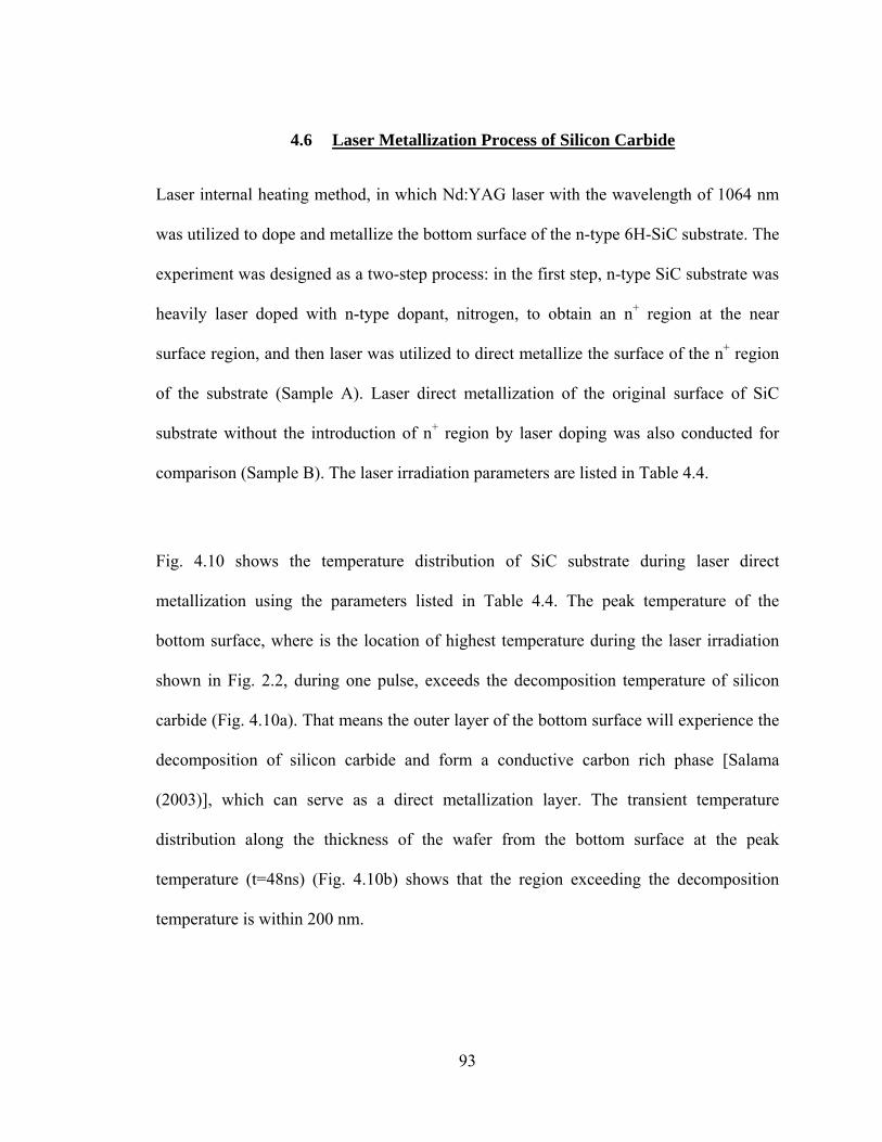
93
4.6 Laser Metallization Process of Silicon Carbide
Laser internal heating method, in which Nd:YAG laser with the wavelength of 1064 nm
was utilized to dope and metallize the bottom surface of the n-type 6H-SiC substrate. The
experiment was designed as a two-step process: in the first step, n-type SiC substrate was
heavily laser doped with n-type dopant, nitrogen, to obtain an n+ region at the near
surface region, and then laser was utilized to direct metallize the surface of the n+ region
of the substrate (Sample A). Laser direct metallization of the original surface of SiC
substrate without the introduction of n+ region by laser doping was also conducted for
comparison (Sample B). The laser irradiation parameters are listed in Table 4.4.
Fig. 4.10 shows the temperature distribution of SiC substrate during laser direct
metallization using the parameters listed in Table 4.4. The peak temperature of the
bottom surface, where is the location of highest temperature during the laser irradiation
shown in Fig. 2.2, during one pulse, exceeds the decomposition temperature of silicon
carbide (Fig. 4.10a). That means the outer layer of the bottom surface will experience the
decomposition of silicon carbide and form a conductive carbon rich phase [Salama
(2003)], which can serve as a direct metallization layer. The transient temperature
distribution along the thickness of the wafer from the bottom surface at the peak
temperature (t=48ns) (Fig. 4.10b) shows that the region exceeding the decomposition
temperature is within 200 nm.

94
Table 4.4 Processing parameters for laser direct metallization.
Sample A B
Steps 1 2 1
Method Laser dope Laser metallization
Laser metallization
Laser source Nd:YAG Nd:YAG Nd:YAG
Wavelength (nm) 1064 1064 1064
Pulse repetition rate (Hz)
3000 3000 3000
Beam area (cm2) π(0.03)2/4 π(0.03)2/4 π(0.03)2/4
Pulse energy (mJ)
4 4.33 4.33
Laser fluence (J/cm2)
5.65 6.1 6.1
Pulse intensity (MW/cm2)
78.6 85.1 85.1
Scanning speed (mm/s)
1 1 1
Irradiation passes 1 1 1
Ambient gas N2 at 30 psi Ar at 30 psi Ar at 30 psi

95
0 20 40 60 80 100 120 140 160 180 2000
400
800
1200
1600
2000
2400
2800
3200
3600
Tem
pera
ture
(K)
Time (ns)
3100 K
(a)
268.0 268.2 268.4 268.6 268.8 269.0 269.2 269.4 269.6 269.8 270.01000
1200
1400
1600
1800
2000
2200
2400
2600
2800
3000
3200
3400
Tem
pera
ture
(K)
Depth along the thickness of the wafer (μm)
3100K
(b)
Figure 4.10 Temperature distribution of 6H-SiC during laser direct metallization using
the parameters listed in Table 4.4.(a) Bottom surface temperature distribution with the
time; (b) Transient temperature distribution along the thickness of the wafer from the
bottom surface at the peak temperature (t=48ns).

96
4.7 Realization of Laser Direct Metallization on the Surface of Silicon Carbide
Using the processing parameters listed in Table 4.4, two different electrode structures are
fabricated in n-type 6H-SiC substrates shown in Fig. 4.11: laser direct metallized contacts
fabricated on laser heavily doped n+ substrate (Fig. 4.11a, specimen A) and laser direct
metallized contacts fabricated on original substrate (Fig. 4.11b, specimen B). The doping
profile of laser heavily doped n+ region can be found in Fig. 4.4, where the substrate was
doped to the thickness of 800 nm with a very high surface dopant concentration (1×10²¹
cm-3). Ni ohmic contacts were also marked and deposited on original SiC substrate (Fig.
4.11c, specimen C) by DC magnetron sputtering as reference ohmic contacts to judge on
the behavior of the laser generated contacts. To assure the ohmic behavior of the Ni-SiC
contact, a high temperature annealing (at 1050°C for 5 min.) was conducted in argon
[Porter, (1995)] after the Ni contact deposition. The sizes of all the electrodes are 400 μm
× 400 μm and the distances between two electrodes are about 300 μm.

97
(a) (b) (c)
Figure 4.11 Electrode structures in n-type 6H-SiC substrates by different processing: (a)
laser direct metallized contacts fabricated on laser heavily doped n+ substrate (specimen
A); (b) laser direct metallized contacts fabricated on original substrate (specimen B); (c)
Ni contacts deposited on original substrate (specimen C).
n n n
Laser doped n+ region
Laser metallized contact Laser metallized contact Ni contact
6H-SiC
6H-SiC 6H-SiC

98
The performance of laser direct metallization of carbon rich contacts in the SiC substrates
can be evaluated by comparing the current-voltage (I-V) characteristics of the laser direct
metallized electrodes with those of electrodes fabricated by Ni deposition. The I-V
measurements were conducted by contacting the microprobes of the I-V measurement
instruments directly on the electrodes.
Fig. 4.12 shows that the current-voltage characteristics between the two separated
electrodes on the SiC substrate formed by three different methods at room temperature.
These results show that all of the contacts between the SiC substrate and the electrodes
have ohmic properties, indicating that we have succeeded in the formation of the laser
direct metallized ohmic contacts on SiC substrate. However, the ratios of the rise of
current to the applied voltage for the electrodes formed by the laser direct metallized
methods (specimens A and B) are less than 0.7 of the Ni deposited one, which means the
contact resistances of laser direct metallized contacts are higher than that of Ni deposited
contacts. This may be due to the degradation of the surface layer, i.e., the surface
decomposition layer could perturb the contact performance, such as a voltage drop across
the electrode to the substrate [Eryu et al. (1997)]. On the other hand, laser direct
metallized electrodes formed on heavily doped n+ substrate increase the ratio of the rise
of current to the applied voltage from 0.49 of that of the Ni deposited electrodes (data for
the laser direct metallized electrodes on original substrate) to 0.67 of that of the Ni
deposited ones. This means the combination of laser direct metallization and laser doping
improve the performance of laser direct metallized contacts dramatically. Defects such as
vacancies created during laser doping process may be associated with an enhanced

99
electron concentration underneath the contacts to promote tunneling in the substrate, and
defect-assisted tunneling or recombination by point defects near the surface and well
within the band gap may also contribute to the improvement of laser direct metallized
ohmic contact on laser doped SiC substrate [Mohammad et al. (2005)].
The current-voltage characteristics between the two separated electrodes on the SiC
substrate formed by these three methods at elevated temperatures (150 °C and 250 °C)
are shown in Fig. 4.13. The ohmic behaviors of all the three kinds of electrodes improve
with the increase of temperature indicating the specific contact resistances for all three
cases decrease with the increase of temperature. Compared to the I-V characteristics of
all the three cases at room temperature, same conclusion can be drawn, i.e., the
performances of laser direct metallized contacts are comparable to that of Ni deposited
contacts and combination of laser direct metallization with laser doping improve the
performance of laser direct metallized contacts.
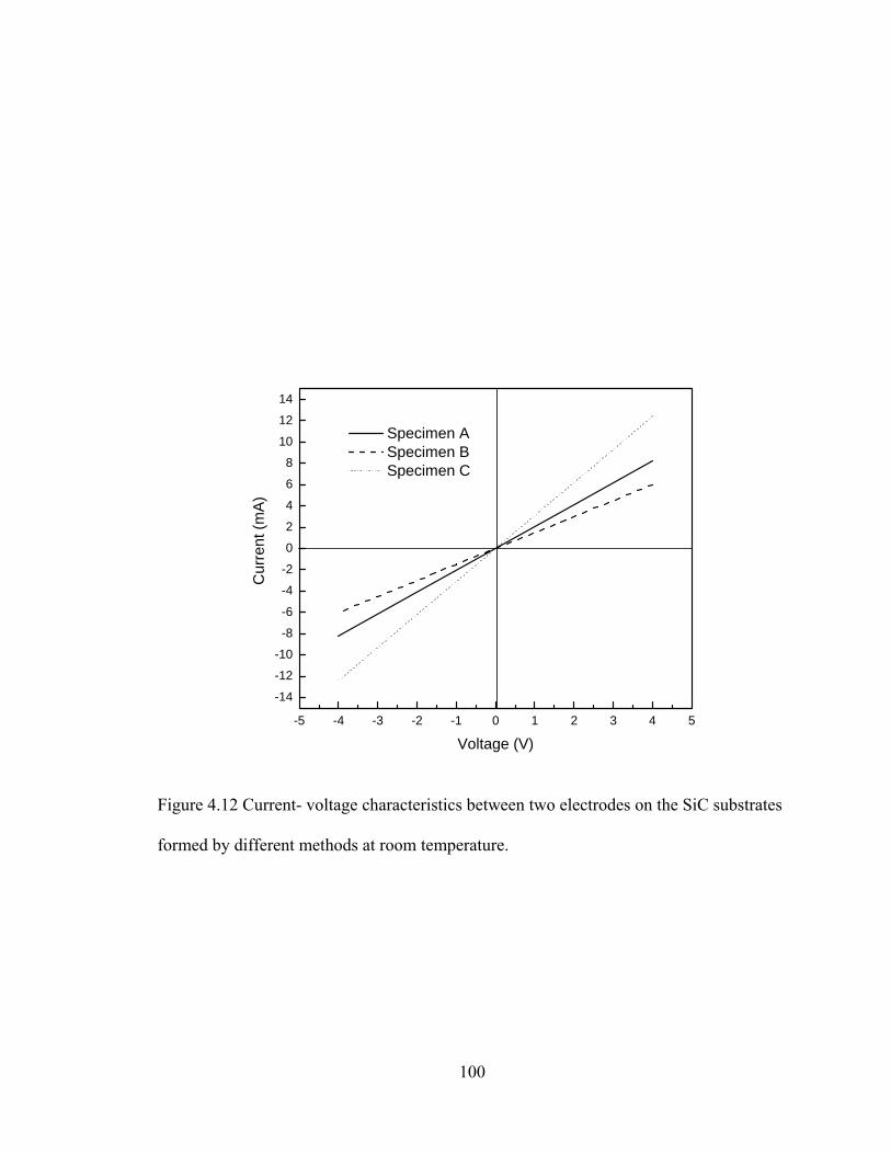
100
-5 -4 -3 -2 -1 0 1 2 3 4 5
-14
-12
-10
-8
-6
-4
-2
0
2
4
6
8
10
12
14
Cur
rent
(mA)
Voltage (V)
Specimen A Specimen B Specimen C
Figure 4.12 Current- voltage characteristics between two electrodes on the SiC substrates
formed by different methods at room temperature.

101
-2 -1 0 1 2
-10
-8
-6
-4
-2
0
2
4
6
8
10
Cur
rent
(mA
)
Voltage (V)
Specimen A Specimen B Specimen C
(a)
-2 -1 0 1 2
-20
-15
-10
-5
0
5
10
15
20
Cur
rent
(mA
)
Voltage (V)
Specimen A Specimen B Specimen C
(b)
Figure 4.13 Current- voltage characteristics between two electrodes on the SiC substrates
formed by different methods at elevated temperatures: (a) 150 °C; (b) 250 °C.
102
5 CHAPTER 5: FABRICATION OF ENDOLAYER AND PIN DIODES OF SILICON CARBIDE
5.1 Introduction
Pulsed laser can be used to produce epilayer by transforming an amorphous or disorder
layer on a crystalline substrate into a thin crystalline layer, which is called pulsed laser-
induced epitaxy (PLIE). PLIE can be described as a two-step process. Firstly, a target
layer with unnecessary high quality crystalline and homogeneity is grown on top of a
semiconductor substrate. In a second step a pulsed laser induces melting/solidification
cycles to transform the top layer into a thin crystalline layer [Boulmer, et al. (1998)]. This
technique has been successfully used to realize SiGeC/Si heterostructures [Boulmer, et al.
(1995) and Kramer and Thompson. (1996)] and, GaP homoepitaxy [Solanki, et al.
(1988)]. The application of this technique to single crystal silicon carbide, however, has
not been reported because silicon carbide does not melt under equilibrium conditions at
the normal pressure [Scace and Slack (1959)].
In this chapter an endotaxial layer was created by incorporating carbon into an epilayer-
free SiC substrate with a pulsed laser using LISPD method. Carbon atoms are introduced
into the top layer of an n-type SiC substrate to form a high resistance endolayer for
various applications such as device isolation and high voltage blocking. The wafer is not
melted in the LISPD method because this process is based on the solid-state diffusion for
103
dopant atoms into the wafer. The dopant precursor can be either a dopant film deposited
on the wafer surface or a dopant gas (dopant-containing vapor) such as an organometallic
compound surrounding the wafer in the processing chamber. The substrate is heated with
a laser beam to diffuse the dopant atoms from the film or to cause pyrolytic
decomposition of the dopant gas producing the dopant atoms that diffuses into the wafer.
SiC PIN diodes were also fabricated by laser doping different mediums including this
endolayer and a parent homoepitaxial SiC layer grown by the conventional chemical
vapor deposition (CVD) method. The performances of these diodes were compared with
others’ PIN diodes fabricated using epilayers and other doping techniques.
5.2 Fabrication of Endolayers in N-Type 6H-SiC Substrates
5.2.1 Experimental Procedures
An n-type 6H-SiC substrate with nitrogen dopant concentration of 5×10¹⁸ atoms/cm3 was
used to fabricate endolayers by incorporating carbon atoms into the top layer of the
substrate using an excimer laser. This process relies on the principle that some of the
nitrogen atoms diffuse out of the substrate during laser irradiation and the incorporated
carbon atoms occupy the vacant sites left behind by the nitrogen atoms. The carbon
atoms can also occupy other vacancies as well as defect sites that might have been
present in the parent substrate. The endotaxy process thus allows improvement of the

104
crystal lattice to an intrinsic semiconductor bond structure. Silicon atoms can also be
incorporated into the SiC substrates to balance the deficiency of silicon atoms in the
substrate. The incorporation of carbon and silicon atoms, therefore, provides a
mechanism of improving the crystalline quality at the substrate surface.
An experimental set-up for laser endolayer fabrication and doping of the substrate is
presented in Fig. 3.2. A laser beam irradiates the substrate placed in a vacuum chamber,
while an appropriate gas, such as methane (CH4) for carbon incorporation or
trimethylaluminum ((CH3)3Al) for aluminum doping of SiC, is passed through the
chamber. A convex lens of focal length 250 mm is used to create different focused spots
on the substrate surface. Various laser processing parameters are listed in Table 5.1. KrF
and ArF excimer lasers of wavelengths 248 and 193 nm respectively were used for
endolayer fabrication by incorporating carbon using methane as the precursor gas.
5.2.2 Carbon Source
Methane is generally cracked into carbon and hydrogen atoms through pyrolytic
decomposition at relatively low temperatures (500 - 800°C) using specific catalysts
[Fukada, et al. (2004)]. Although no special catalyst was used in this study, the pyrolysis
of methane may occur at the laser-heated substrate surface at high temperatures. The
photolysis of methane is also possible due to its interaction with the photons of the laser
beam. These two chemical reactions can be written as follows.
Pyrolytic decomposition [Sharma et al. (1999)]:

105
Table 5.1 Laser processing parameters for endotaxy experiments.
Endolayer formation Endolayer formation
Laser source KrF excimer ArF excimer
Wavelength (nm) 248 193
Pulse length (ns) 25 20
Pulse energy (mJ) 75 50
Laser fluence (J/cm2) 1.5 1
Pulse intensity (MW/cm2) 60 50
Pulse repetition rate (Hz) 1 1
Laser shots 600 600
Beam area (cm2) 0.2×0.25 0.2×0.25
Ambient gas Methane at 30 psi Methane at 30 psi

106
212001000
4 2)( HsCCH Co
+⎯⎯⎯⎯ →⎯ − , ΔH = 74.9 kJ/mol (5.1)
Photolytic decomposition [Mazumder and Kar (1995)]:
)( 2)( ) 3.4( )( 24 gHsCeVhgCH +→+ ν (5.2)
The substrate surface peak temperature can be estimated using the following expression
[Tian, et al. (2005)]:
tk
AITtT l
πα2
)( 0 += for t ≤ tp. (5.3)
Here T(t) is the peak temperature at any time t as the laser irradiation progresses, T0 is
the initial temperature of the substrate, Il is the laser irradiance, A is the absorptivity
which is taken as 0.71 and 0.58 at the wavelengths of 248 and 193 nm respectively for
6H-SiC [Levinshtein, et al. (2001)], α is the thermal diffusivity which is 2.2 cm2s-1 for
6H-SiC, k is the thermal conductivity which is 4.9 Wcm-1°C-1 for 6H-SiC and tp is the
laser pulse length. For laser irradiances of 60 and 50 MW/cm2 during KrF and ArF laser
endotaxy experiments respectively, the corresponding peak temperatures are estimated to
be 2330°C and 1430°C.
Since these temperatures are much higher than the pyrolytic decomposition temperature
as given in chemical reaction (5.1), the pyrolysis of methane is expected to occur in the
present case. Since the carbon atoms are removed from the reaction product due to their
diffusion into the substrate, reaction (5.1) will proceed in the forward direction under
nonequilibrium conditions, which generally increases the reaction yield. On the other
hand, photolytic reaction (5.2) is also expected to occur in the present case since the
energy of a photon of the KrF and ArF excimer lasers are 5 and 6.4 eV respectively,

107
which are higher than the energy of a carbon-hydrogen bond (413 kJ/mole, i.e., 4.3 eV) in
methane [Speight (2003)]. So both the pyrolytic and photolytic reactions will contribute
to the formation of carbon atoms from methane for the formation of endolayers.
5.2.3 Hydrogen removal from the endolayer
It should be noted that both carbon and hydrogen atoms are generated in the chemical
reaction and both of them can diffuse into the substrate. To produce contamination-free,
i.e., hydrogen-free endolayers, the samples were annealed at 1000 °C for 10 min in an Ar
ambient after the laser endotaxy experiment in order to diffuse out the hydrogen atoms.
Fig 5.1 shows the concentrations of hydrogen in the endolayer, annealed endolayer and
parent wafer measured by SIMS. The endolayer samples are prepared by KrF excimer
laser irradiation. It indicates that the annealing process reduces the hydrogen
concentration to the background level of the parent sample. The data in this figure are
normalized by the silicon concentration in the silicon carbide substrate. During carbon
incorporation hydrogen atoms also diffuse into the substrate with the peak normalized
concentration of 0.45% decreasing to 0.15% at the depth of 300 nm. After annealing the
SiC endolayer at 1000 °C for 10 min, almost all of the hydrogen atoms diffuse out of the
substrate; the hydrogen concentration decreases to the original content in the parent
substrate.

108
0 50 100 150 200 250 300 350
10-3
10-2
10-1
Nor
mal
ized
Con
cent
ratio
n of
Hyd
roge
n
Depth (nm)
1 Parent wafer2 Endolayer3 Annealed endolayer
1
23
Figure 5.1 Comparison of the hydrogen content in a 6H-SiC sample of three different
qualities.

109
5.2.4 Determination of the Thickness and Crystalline Order of the Endolayer
To examine the effect of laser processing on the crystalline order of the endolayer, TEM
images of an annealed endolayer that was prepared by ArF excimer laser irradiation were
compared with those of the parent wafer. The samples were sputter-coated with a ~ 40
nm Au layer using an Emitech K550 sputtering equipment. A Focused Ion Beam (FIB)
instrument was used to obtain cross-sections of these samples in order to prepare TEM
specimens. Platinum film was deposited by Ga+ ion beam-assisted CVD as a protective
layer for subsequent FIB milling operation. The TEM studies were carried out with a FEI
Tecnai F30 TEM operating at 200 keV with x-ray energy dispersive spectrometry
(XEDS). The thickness of the endolayer was measured by XEDS.
Figures 5.2a and b show two XEDS scanning line with four points a, b, c and d on each
line for the endolayer and parent samples respectively. The carbon concentrations along
these lines were measured by XEDS equipped with the TEM instrument, and the data are
presented in Fig. 5.2c. The XEDS scan starts from the platinum film (point a) and ends at
a depth of about 400 nm in the bulk of the SiC substrate (point d) for both samples as
shown in Figs. 5.2a and b. Comparing the carbon counts of these two samples in Fig.
5.2c, it can be observed that the carbon concentration is nearly constant in the parent
sample whereas the endolayer specimen exhibits a carbon-rich region. This region is
bounded between two vertical dashed lines in Fig. 5.2c, at the depths of 65 and 163 nm
corresponding to points b and c respectively in Fig. 5.2a. So the endolayer can be

110
(a)
(b)
Carbon contamination by irradiation of electron beam
6H-SiC Cross section
Gold film deposited for TEM
Platinum film deposited for FIB
200 nm
a b c d
Reference image for drift correction
Top
surf
ace
of
the
spec
imen
Bot
tom
surf
ace
of th
e sp
ecim
en
Top
surf
ace
of
the
spec
imen
Bot
tom
surf
ace
of th
e sp
ecim
en
6H-SiC Cross section
Gold film deposited for TEM
Platinum film deposited for FIB
200 nm
a b c dReference image for drift correction

111
0 100 200 300 400 500
20
40
60
80
100
120C
arbo
n C
ount
s
Position (nm)
Annealed endolayer Parent wafer
a c db
(c) XEDS data for carbon counts along the depth of the specimens.
Figure 5.2 XEDS analysis for the carbon contents along the depth of both annealed
endolayer specimen and parent wafer: (a) XEDS scanning line showing four locations a,
b, c and d along the depth of the endolayer specimen; (b) XEDS scanning line showing
four locations a, b, c and d along the depth of the parent specimen; (c) XEDS data for
carbon counts along the depth of the specimens. The four locations a, b, c and d are
marked on these data to show higher carbon content in the endolayer than in the parent
specimen, indicating carbon incorporation into the wafer during the endotaxy experiment.

112
considered to be about 100 nm thick, containing a larger amount of carbon than the
parent substrate.
TEM images of the cross-sections of an annealed endolayer and a parent substrate are
presented in Fig. 5.3 to show that the laser endotaxy process does not generate defects in
the substrate. Fig. 5.3a shows an amorphous layer of thickness of ~17 nm at the surface
of the annealed endolayer specimen. A similar amorphous layer is also present at the
surface of the parent wafer in Fig. 5.3b, indicating that amorphization is not due to the
laser processing. The TEM image at a higher magnification in Fig. 5.4a shows the
integrity of crystalline lattices beneath the amorphous layer, which is comparable to the
crystalline lattices of the parent wafer in Fig. 5.4b.
The amorphous layers in both types of specimen may have formed during the deposition
of the platinum film that was used as a protective layer for subsequent FIB milling of the
sample to produce TEM specimen. Although a gold film was directly deposited on top of
the SiC substrate, the platinum film deposition process is expected to amorphize the
specimens as explained below. The platinum film was deposited by Ga+ ion beam-
assisted chemical vapor deposition using an accelerating voltage of 30 kV with 2.2 μA
beam current. Lipp et al [Lipp, et al (1996)] and Kempshall et al [Kempshall, et al
(2002)] reported amorphous layers of thickness 40-50 nm on silicon substrates due to
platinum deposition with a 30 kV Ga+ ion beam. Even a sputter-deposited 70 nm thick
Au-Pd coating on a silicon substrate could not completely prevent the substrate damage
during the subsequent 30 kV Ga+ ion beam-assisted platinum deposition [Kempshall, et

113
(a)
(b)
Figure 5.3 TEM images of cross-sections of an annealed endolayer and parent wafer: (a)
Observed amorphous layer in the endolayer specimen; (b) Observed amorphous layer in
the parent wafer.
10 nm
Gold film deposited for TEM
Amorphous layer
6H-SiC Crystal lattice
Gold film deposited for TEM
Amorphous layer
6H-SiC Crystal lattice
10 nm

114
(a)
(b)
Figure 5.4 High-resolution TEM images of cross-sections of an annealed endolayer and
parent wafer: (a) The interface between damaged amorphous and crystalline SiC of the
endolayer specimen; (b) The interface between damaged amorphous and crystalline SiC
of the parent wafer.
2 nm
2 nm
Amorphous layer
Amorphous layer
6H-SiC Crystal lattice
6H-SiC Crystal lattice

115
al (2002)]. In our studies, gold coatings of thicknesses 41 and 44 nm were sputter-
deposited on the endolayer (Fig. 5.2a) and parent (Fig. 5.2b) samples respectively to
prevent any substrate damage during the subsequent platinum film deposition process,
but the gold films were evidently not thick enough to prevent amorphization at the
sample surface.
The aligned and random RBS channeling spectra of endolayer and annealed endolayer
specimens that are prepared by KrF excimer laser irradiation as well as the parent wafer
are also compared to analyze the lattice disorder of this laser-induced solid phase
diffusion process, which are shown in Figs. 5.5-5.7, respectively. The aligned spectra for
the endolayer specimen and annealed endolayer specimen are very similar to the one for
the parent wafer, indicating no evident damage to the lattices occurs during the laser-
induced solid phase diffusion process. The RBS data also shows the crystalline integrity
of the endotaxy process.
Al, N, He and H ion implantations have been reported to cause amorphization in SiC
[Canut, et al. (1997) and Musumeci, et al. (1996)]. RBS channeling spectra [Canut et al.
(1997)] showed that aluminum ion implantation in SiC at room temperature (maximum
Al concentration of about 5 × 1019 cm-3 and implantation depth of 50 nm) induced
amorphization in the substrate and a general decrease of the backscattering yield was
observed in the channeling region after annealing. The relative disorder remained large
(80%) near the sample surface in spite of annealing at high temperatures. Nitrogen ion

116
Figure 5.5 The aligned and random RBS channeling spectra of parent 6H-SiC sample.
1 0 0 200 300 400 50 0 6 0 0Channel
0
5
1 0
1 5
2 0
0 . 4 0.6 0.8 1.0 1.2 1 . 4 Energy (MeV)
1
2
3
. .
1 Parent wafer random 2 RUMP simulation 3 Parent wafer aligned
Nor
mal
ized
Yie
ld

117
Figure 5.6 The aligned and random RBS channeling spectra of endolayer specimen.
1 0 0 200 300 400 5 0 6 0 0 Channel
0
5
1 0
1 5
2 0 0 . 4 0.6 0.8 1.0 1.2 1 . 4
Energy (MeV)
1
2
3
1 Endolayer specimen random 2 RUMP simulation 3 Endolayer specimen aligned
Nor
mal
ized
Yie
ld

118
Figure 5.7 The aligned and random RBS channeling spectra of annealed endolayer
specimen.
1 0 0 200 300 400 500 6 0 0 Channel
0
5
1 0
1 5
2 0 0 . 4 0.6 0.8 1.0 1.2 1 . 4
Energy(MeV)
1
2
3
1 Annealed endolayer specimen random 2 RUMP simulation 3 Annealed endolayer specimen aligned
Nor
mal
ized
Yie
ld
119
implantation at room temperature (maximum nitrogen concentration of about 5 × 10²⁰
cm-3 and implantation depth of 450 nm) also amorphizes SiC [Kimoto, et al. (1997)].
Amorphization is caused by the elastic collisions of dopant atoms with the wafer lattice
atoms and the long range order disappears when the threshold ion dose (φth) is exceeded
during ion implantation. The amorphization process involves point defect accumulation
[Musumeci, et al. (1996)], whereas annealing allows partial recrystallization of the
amorphous phase [Canut, et al. (1997)]. Laser induced solid phase diffusion process does
not cause amorphization due to different doping mechanism compared to the case of ion-
implanted doping. Laser induced solid phase diffusion utilizes laser-heating to
incorporate and diffuse impurities in a wafer. It is a diffusion-based process and elastic
collisions between the dopant atoms and SiC lattice atoms are not evident.
5.2.5 Determination of the Resistivity of the Endolayer
To examine the resistivity of the endolayer, the I-V characteristics of the parent wafer,
endolayer and the annealed endolayer samples that were prepared by ArF excimer laser
irradiation were analyzed. For electrical characterization, Ni contacts were formed on
both sides of an endolayer sample, an annealed endolayer sample and a parent 6H-SiC
wafer using e-beam evaporation. The samples were annealed after Ni deposition at
1000°C for 1 min [Porter and Davis (1995)] for Ohmic contact. The current-voltage (I-V)
measurements were performed using a Tektronix 576 curve tracer by contacting the Ni
deposits with microprobes.

120
The samples are treated as a composite structure consisting of the contacts, endolayer and
substrate in the case of endolayer samples and only the contacts and substrate in the case
of the parent sample. The resistances of the endolayer samples (Rtotal) obtained from I-V
measurements are the sums of the resistances of the endolayer (Re), contacts (Rc) and
substrate (Rs) [Nadella and Capano (1997)], i.e.,
scetotal RRRR ++= (5.4)
Knowing Rtotal and the sum of the contacts and substrate of the parent sample, which
yields the value of Rc + Rs, the resistances of both types of endolayer samples (Re) are
obtained from Eq. (5.4), and listed in Table 5.2. The resistivities of the endolayers (ρe)
are estimated using the expression [Edwards, et al. (1997)], ρe = ReANi/de, where ANi is
the area of the top Ni contact and de is the thickness of the endolayer. The value of de is
determined as 100 nm from the XEDS data. The resistivities of the endolayer samples are
also listed in Table 5.2 including the resistivities of intrinsic (pure) Germanium and
Silicon for comparison. The resistivity of the endolayer is 1.1 × 10⁵ Ω·cm, which is much
higher than the resistivity needed for device isolation, 2 × 10⁴ Ω·cm [Nadella and Capano
(1997)]. After annealing, the resistivity of the sample decreases slightly to 9.4 × 10⁴
Ω·cm, which may be due to the out-diffusion of hydrogen atoms thus losing any
passivation caused by these atoms. Typical range of resistivities for insulators,
semiconductors and conductors including silicon carbide is shown in Fig. 5.8 [Sze,
(2001)].
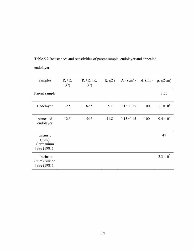
121
Table 5.2 Resistances and resistivities of parent sample, endolayer and annealed
endolayer.
Samples Rc+Rs (Ω)
Re+Rc+Rs (Ω)
Re (Ω) ANi (cm2) de (nm) ρe (Ωcm)
Parent sample 1.55
Endolayer 12.5 62.5 50 0.15×0.15 100 1.1×10⁵
Annealed endolayer
12.5 54.3
41.8 0.15×0.15 100 9.4×10⁴
Intrinsic (pure)
Germanium [Sze (1981)]
47
Intrinsic (pure) Silicon [Sze (1981)]
2.3×10⁵

122
Figure 5.8 Typical range of resistivities for insulators, semiconductors and conductors.
123
5.3 Fabrication of PIN Diodes on Substrates with an Endolayer
To fabricate PIN diodes, a p-type dopant, aluminum was incorporated into the annealed
endolayer using a KrF excimer laser (Fig. 5.9a). Trimethylaluminum was used as the
precursor for the aluminum dopant atoms. The laser doping parameters are listed in Table
5.3. To compare the performance of the PIN diode to another device that does not contain
the insulator region, a p-n junction was fabricated as a reference sample (Fig. 5.9b) by
doping the parent n-type SiC substrate with aluminum using the same laser processing
method and parameters as for the PIN diode in Fig. 5.9a. This allows evaluation of the
effectiveness of the insulator region in the PIN diode.

124
Table 5.3 Laser processing parameters for p-type doping on the endolayer and parent
substrate.
P-type doping on endolayer (PIN
Diode)
P-type doping on parent substrate
(p-n junction)
Laser source KrF excimer KrF excimer
Wavelength (nm) 248 248
Pulse length (ns) 25 25
Pulse energy (mJ) 75 75
Laser fluence (J/cm2) 1.5 1.5
Pulse intensity (MW/cm2) 60 60
Pulse repetition rate (Hz) 1 1
Laser shots 300 300
Beam area (cm2) 0.2×0.25 0.2×0.25
Ambient gas TMA at 30 psi TMA at 30 psi

125
(a) (b)
Figure 5.9 Device designs on SiC substrates with and without an endolayer: (a) PIN
diode on laser-formed endolayer and (b) reference p-n junction.
Al/Ti contact
n
p doped 70 nm junction depth
Al/Ti contact
Endolayer 30 nm
PIN Diode
6H-SiC
Al/Ti contact
Al/Ti contact
p doped 70 nm junction depth
n
P-n Junction
6H-SiC

126
Laser doping of aluminum was carried out by focusing the KrF excimer laser beam of
wavelength 248 nm on the wafer segment with a beam area 2×2.5 mm2, laser fluence 1.5
J/cm2, repetition rate 1 Hz and laser pulses 300. The doped samples were cleaned by
immersion in a KOH solution for several minutes to remove the aluminum residue
formed on the wafer surface during the laser doping experiment. The laser doped regions
were cut into planar diodes with a size of 1.5 × 1.5 mm2. Ohmic contacts were formed by
depositing Al/Ti on the top and bottom sides of the sample using an Edwards Thermal
Evaporator and by annealing at 1000°C for 5 min. The I-V characteristics of the PIN
diodes were measured using micromanipulators connected to a Tektronix 576 curve
tracer.
Fig. 5.10 shows SIMS data for laser-doped aluminum concentration in the endolayer of a
6H-SiC substrate. The endolayer was doped to a depth of 70 nm with maximum dopant
concentration 1 × 10²¹ atoms/cm3. Fig. 5.11 shows the I-V characteristics of a laser-
fabricated endolayer PIN diode and a reference p-n junction in parent 6H-SiC. The p-n
junction exhibits the rectifying property of a typical diode with high forward current and
relatively low leakage current. Considering a leakage current density of 10-2 A/cm2 as a
threshold, which is generally used for defining blocking voltage in standard commercial
Si power devices [Singh, et al. (2002)], the breakdown voltage of the p-n junction is
found to be about 13 V. The forward current of the endolayer PIN diode is much lower
than that of the p-n junction because of the high resistance of the endolayer. The leakage
current of the diode is also reduced compared to that of the p-n junction and the

127
breakdown voltage of the diode is found to be about 18 V based on the same leakage
current density threshold as above.
0 20 40 60 80 100 120 1401017
1018
1019
1020
1021
Alu
min
um d
opan
t con
cent
ratio
n (c
m-3)
Depth of the SiC wafer (nm)
1 Background2 Al dopant profile in endolayer
1
2
Figure 5.10 Depth profiles of aluminum concentration in the top laser-doped p region in
the endolayer measured by SIMS.

128
Figure 5.11 I-V characteristics of PIN diodes fabricated on an endolayer and a parent 6H-
SiC.

129
5.4 Fabrication of PIN Diodes on Substrates with Epilayer
Prototype SiC PIN diodes with a size of 0.5 × 0.5 mm2 were fabricated on n-type 4H-SiC
wafer segments with a 10 μm thick epitaxial layer containing a donor concentration in the
range of 8× 10¹⁵ to 1.3×1016 cm-3. A reference Schottky diode was also fabricated to
evaluate the effect of epilayer laser doping parameters on PIN diode performance.
Schematics of the diodes are presented in Fig. 5.12. Two different structures are used for
the diode fabrication: (1) a laser aluminum doped top p region on the mentioned substrate
(Diode A, Fig. 5.12a); (2) same laser doped top p region on the same substrate with
different laser pulses (1000 and 3000 for Diodes B and C respectively) and a laser direct
metallized bottom (Diode B in Fig. 5.12b and Diode C in Fig. 5.12c). The top p region
was aluminum doped by using surface heating doping method, and the laser direct
metallized bottom regions were fabricated using a Nd:YAG laser internal heating
method, both of which have been discussed in Chapter 4. Laser processing parameters for
p-type doping and laser direct metallization on the Diodes are shown in Table 5.4. Au/Pt
was sputtered onto the top laser doped p+ region of all three diodes (Diodes A, B and C)
and bottom of the substrate of Diode A to create a metal thin film ohmic contact; for
Diodes B and C the laser direct metallized bottom regions has been created carbon rich
ohmic contacts which were contacted directly by the microprobes of the I-V
measurement instruments. The reference Schottky diode (Diode D, Fig. 5.12d) was
fabricated by sputtering Au/Pt on both low doped epitaxial layer surface and substrate
bottom. Au/Pt sputtered on such low doped epilayer surface (8× 10¹⁵ to 1.3×1016 cm-3)
can not form ohmic contact and only Schottky contact can be formed with the SiC
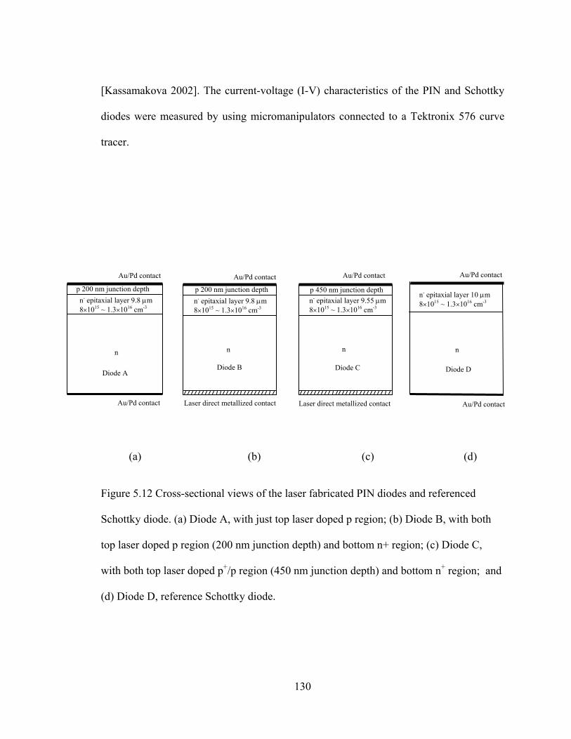
130
[Kassamakova 2002]. The current-voltage (I-V) characteristics of the PIN and Schottky
diodes were measured by using micromanipulators connected to a Tektronix 576 curve
tracer.
(a) (b) (c) (d)
Figure 5.12 Cross-sectional views of the laser fabricated PIN diodes and referenced
Schottky diode. (a) Diode A, with just top laser doped p region; (b) Diode B, with both
top laser doped p region (200 nm junction depth) and bottom n+ region; (c) Diode C,
with both top laser doped p+/p region (450 nm junction depth) and bottom n+ region; and
(d) Diode D, reference Schottky diode.
Au/Pd contact
n
p 200 nm junction depth
Au/Pd contact
n- epitaxial layer 9.8 μm 8×10¹⁵ ~ 1.3×1016 cm-3
Diode A
Au/Pd contact
n
n- epitaxial layer 9.8 μm 8×10¹⁵ ~ 1.3×1016 cm-3
p 200 nm junction depth
Laser direct metallized contact
Diode B
Laser direct metallized contact
Au/Pd contact
n
n- epitaxial layer 9.55 μm 8×10¹⁵ ~ 1.3×1016 cm-3
p 450 nm junction depth
Diode C
n
Au/Pd contact
n- epitaxial layer 10 μm 8×10¹⁵ ~ 1.3×1016 cm-3
Diode D
Au/Pd contact
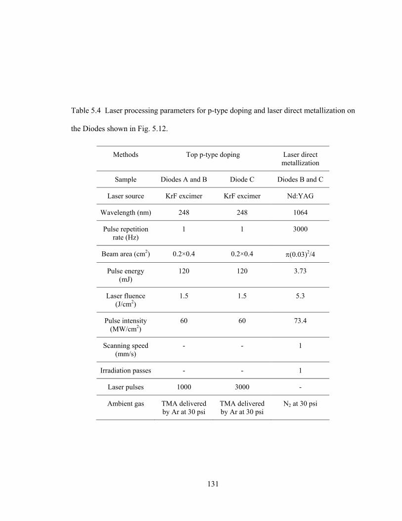
131
Table 5.4 Laser processing parameters for p-type doping and laser direct metallization on
the Diodes shown in Fig. 5.12.
Methods Top p-type doping Laser direct metallization
Sample Diodes A and B Diode C Diodes B and C
Laser source KrF excimer KrF excimer Nd:YAG
Wavelength (nm) 248 248 1064
Pulse repetition rate (Hz)
1 1 3000
Beam area (cm2) 0.2×0.4 0.2×0.4 π(0.03)2/4
Pulse energy (mJ)
120 120 3.73
Laser fluence (J/cm2)
1.5 1.5 5.3
Pulse intensity (MW/cm2)
60 60 73.4
Scanning speed (mm/s)
- - 1
Irradiation passes - - 1
Laser pulses 1000 3000 -
Ambient gas TMA delivered by Ar at 30 psi
TMA delivered by Ar at 30 psi
N2 at 30 psi

132
The doping profiles of top p doped regions in Diodes A-C have been discussed in Section
4.3.2, in which 200 nm and 450 nm junction depths were obtained for 1000 and 3000
laser pulses respectively. The temperature distributions of SiC substrate during laser
direct metallization using the parameters listed in Table 5.4 are shown in Fig. 5.13. The
peak temperature of the bottom surface (3268 K) exceeds the peritectic temperature of
silicon carbide (Fig. 5.13a) so the bottom surface will create a carbon rich phase after the
decomposition of silicon carbide and can serve as a direct metallization layer. The
transient temperature distribution along the thickness of the wafer from the bottom
surface at the peak temperature (t=48ns) (Fig. 5.13b) shows that the region exceeding the
decomposition temperature is about 190 nm.

133
0 20 40 60 80 100 120 140 160 180 2000
400
800
1200
1600
2000
2400
2800
3200
3600
Tem
pera
ture
(K)
Time (ns)
3100 K
(a)
268.0 268.2 268.4 268.6 268.8 269.0 269.2 269.4 269.6 269.8 270.01000
1200
1400
1600
1800
2000
2200
2400
2600
2800
3000
3200
3400
Tem
pera
ture
(K)
Depth along the thickness of the wafer (μm)
3100K
(b)
Figure 5.13 Temperature distribution of 4H-SiC during laser direct metallization using
the parameters listed in Table 5.4.(a) Bottom surface temperature distribution with the
time; (b) Transient temperature distribution along the thickness of the wafer from the
bottom surface at the peak temperature (t=48ns).
134
Fig. 5.14 shows the I-V characteristics of the reference Schottky diode (Diode D) (Fig.
5.12a) and three laser fabricated diodes (Fig. 5.12b) at room temperature. Under forward
current the Schottky diode reaches 100 A/cm2 at 19 V and shows an abrupt breakdown
voltage of 320 V when reverse bias is applied. Diode A exhibits a breakdown voltage of
500 V and reaches VF of 20 V at 100 A/cm2. The improved breakdown voltage is
attributed to a new reverse leakage current mechanism. The high leakage current of the
reference Schottky diode is due to majority carriers that overcome the barrier. The PIN
diode suppresses the leakage current resulting from minority carriers diffusing to the
depletion layer.
Diode B decreases the VF at 100 A/cm2 to about 13 V, and Diode C, having a deeper laser
doped p junction depth, exhibits a VF at 100 A/cm2 of 12.5 V, indicating the effectiveness
of the laser direct metallized contact. Although both possess laser doped p region and
laser direct metallized layer, Diode C shows an abrupt breakdown voltage of 460 V while
Diode B does not show abrupt avalanche breakdown but rather a soft breakdown, which
may be due to the different dopant profiles of the p regions doped in the two diodes or the
defects such as micropipes (screw dislocation) and stacking faults in the Diode B cause
its soft breakdown. Using a leakage current density of < 10-2 A/cm2 as a threshold, which
is considered acceptable for defining blocking voltage in standard commercial Si power
devices [Singh, Irvine, et al. (2002)], the breakdown voltage of Diodes B is about 420 V.
The theoretical breakdown voltage of the PIN diode can be estimated by determining the
drift region thickness from the basic depletion equation [Singh, et al. (2002)]:

135
)2
(][ 0200
D
Br
D
r
D
r
NqV
NqEc
NqEc
W⋅
⋅⋅−
⋅⋅⋅
−⋅
⋅⋅=
εεεεεε (5.5)
where BV is the breakdown voltage, W is the drift layer thickness that is taken as the
epilayer thickness, q is the electronic charge, rε is the relative dielectric constant of SiC,
i.e., 72.9=rε [Singh (1994)], 0ε is the permittivity of vacuum, and CE is the critical
electric field which was empirically derived by Konstaitinov [Konstantinov, et al. (1997)]
relating CE to the dopant concentration (ND cm-3) in the epilayer for 4H-SiC wafers, i.e.,
cmVN
ED
c /)
10(log
411
1049.2
1610
6
−
×= (5.6)
Substituting Eq. (5.6) into Eq. (5.5), the following expression is obtained:
0
2
1610
6
2)10
(log411
1049.2εε ⋅⋅⋅
−−
×=
r
D
DB
NqWNWV (5.7)
Considering an average dopant concentration ND = 1×1016 cm-3, an epilayer of thickness
W = 9.8 μm, the theoretical breakdown voltage of the PIN diode is 1547 V. The
measured breakdown voltages of the PIN diodes are about 500 V which are
approximately one third of the theoretical value. This discrepancy may be due to several
reasons:
(a) Lack of proper edge termination and passivation - This can produce concentrated
electric field at the corners of three-dimensional structures leading to early breakdown at
the edges. An effective edge termination is expected to make the electric field distribution
uniform at the edges of the device and therefore increase the breakdown voltage of the
device. It has been reported that the breakdown voltages of SiC Schottky and PIN diodes

136
were improved significantly by different edge termination designs compared to those
without edge termination [Alok, et al. (1994), Itoh, et al. (1996) and Biserica, et al.
(2001)].
(b) Defects such as micropipes (screw dislocation) and stacking faults in the epilayer -
The micropipes are generally aligned along the c-axis of the SiC crystal. Since our
devices had a vertical structure along the thickness of the substrate, the applied electric
field, which could be almost parallel to the c-axis, induces leakage current through the
micropipe defects causing electrical breakdown of the PIN diode at a low voltage [Tin, et
al. (1996)].
The performances of laser-fabricated PIN diodes and conventionally fabricated PIN
diodes are summarized in Table 5.5. The results are comparable to the others’ data
considering the absence of edge termination in the laser-fabricated PIN diodes. These
results indicate the promise of this novel laser direct doping and metallization technique
for the fabrication of SiC PIN diodes.

137
(a)
(b)
Figure 5.14 Measured Schottky diode and PIN diodes I-V curves at room temperature. (a)
Schottky diode. (b) Laser fabricated PIN diodes.

138
Table 5.5 Comparison of the performance of the PIN diodes fabricated in the literatures
and our group.
4H-SiC [Sugawara,
et al. (2001)]
6H-SiC [Fujihira, et al. (2002)]
4H-SiC [Alexandrov, et al. (2001)]
Laser fabricated PIN diode on 4H-
SiC (this work)
Laser fabricated PIN diode on 6H-
SiC (this work)
Fabrication method Epitaxial growth
Epitaxial growth
Ion implantation
Laser doping Laser doping
Epilayer thickness (μm)
200 31 30 9.55, 9.8
Endolayer thickness (μm)
0.03
Dopant concentration in the
epilayer (cm-3)
8×10¹³ 1×10¹⁵ 1×10¹⁵ 8×10¹⁵ ~ 1.3×10¹⁶
Edge termination method
JTE none MJTE none none
Breakdown Voltage (V)
19500 4200 5000 420 ~ 500 18
Ideal breakdown voltage (VB) based
on Eq. (5.7)
29700 5281 5139 1345 ~ 1668
Forward Voltage drop at 100A/cm2
(V)
6.5 3.75 4.2 12.5 ~ 20
JTE: Junction termination extension. MJTE: Multistep junction termination extension.

139
6 CHAPTER 6: LASER SYNTHESIS OF OPTICAL STRUCTURE IN SILICON CARBIDE
6.1 Introduction
Silicon carbide (SiC) is a promising semiconductor material for optical devices,
particularly mirrors and lenses, because of its low thermal coefficient of expansion,
hardness (and hence good polish ability), high thermal conductivity (350-490 Wm-1K-1)
and chemical stability in hostile environments [Goela et al. (1991) and Heft et al. (1995)].
Rohm and Haas Company, Advanced Materials Division, and more recently, Polo
Corporation (circa 2004) are developing silicon carbide as a mirror or mirror coating on
beryllium. The material can be polished to less than 3 Ǻngstrom RMS surface finish and
is resistant to wet oxygen up to 1650°C; Rohm and Haas CVD SiC has a reflectivity of
greater than 41% for wavelengths 120-190 nm and 70-99% for wavelengths ranging form
10500-12000 nm [Goela et al. (1991) and Narushima et al. (1990)). The objectives of this
chapter are 1) to present the laser direct write technique for fabrication of optical
structures in SiC and 2) to characterize the optical properties of the optical structures
created in SiC by this process.
6.2 Laser Synthesis of Embedded Optical Phases
Semi-insulating 6H-SiC with the thickness of 430 μm was used for the synthesis of
embedded optical phase. The laser processing parameters are listed in Table 6.1.

140
Table 6.1 Laser processing parameters for the synthesis of embedded optical phases.
C-rich phase C-rich phase containing nitrogen
C-rich phase containing aluminum
Laser source Nd:YAG Nd:YAG Nd:YAG
Wavelength (nm) 1064 1064 1064
Pulse repetition rate (kHz)
3 3 2
Beam area (cm2) π(0.03)2/4 π(0.03)2/4 π(0.03)2/4
Pulse energy (mJ)
4.7 4.7 5.5
Laser fluence (J/cm2)
6.65 6.65 7.75
Pulse intensity (MW/cm2)
92.3 92.3 118
Scanning speed (mm/s)
1 1 1
Irradiation passes 1 1 1
Ambient gas Ar at 30 psi N2 at 30 psi TMA delivered by Ar at 30 psi

141
The incident focused laser beam is transmitted through the top surface of the 6H-SiC
wafer and most of the laser energy are absorbed by the unpolished bottom surface, as
shown in Fig. 6.1. Since the pulse intensities of all these three cases are higher than the
critical pulse intensity for decomposition of SiC shown in Fig. 2.6, carbon rich phase can
form from the bottom surface toward the bulk [Salama (2003)]. This is a direct write
process. Optical interferometry roughness measurements showed no deterioration in
surface roughness of the embedded optical phase (e.g., a reflector) after this mode of
laser processing; consequently, no post anneal was required [Salama et al. (2002)]. The
fact that the width of the laser written reflector is smaller than the diameter of the incident
focused laser beam is surprising and is not anticipated by Snell’s Law. A plausible
explanation is the activation of nonlinear absorption, which leads to the onset of a self-
focusing effect in SiC wafers on the order of 430 μm thick [Salama (2003)]. An optical
carbon rich phase embedded in a polished single crystalline 6H-SiC substrate is shown in
Fig. 6.2.

142
6H-SiC
Focused laser beam at the surface
Laser beam passing through the bulk
Figure 6.1 Fabrication of an embedded optical structure.

143
Figure 6.2 Silicon carbide substrate showing an embedded optical structure.
100µm
Laser-synthesized optical phase
Original SiC substrate

144
6.3 Optical Property Modification
Such embedded laser-synthesized optical phase was tested for reflectivity using a green
laser (wavelength, λ = 532 nm). The reflectivity of both the laser-synthesized and parent
silicon carbide substrate were found to be 16% and 10% respectively. This is a
reflectance increase of 60% for 532 nm wavelength irradiation, at room temperature.
These promising results led to a literature search on SiC reflectivity. Epitaxial SiC
surfaces (epilayers) have been observed [Goela et al. (1991)] to provide sufficient
reflectivity for signal processing. Our preliminary laser synthesized optical structures
yield comparable results.
In this present study the reflectivity and transmission of the laser synthesized embedded
structures were calculated based on the transmitted (PT) and reflected (PR) powers
measured at a laser wavelength of 1064 nm, whose set-up is illustrated in Fig. 6.3. The
transmitted and reflected powers are measured using detector #1 and detector #2
respectively.
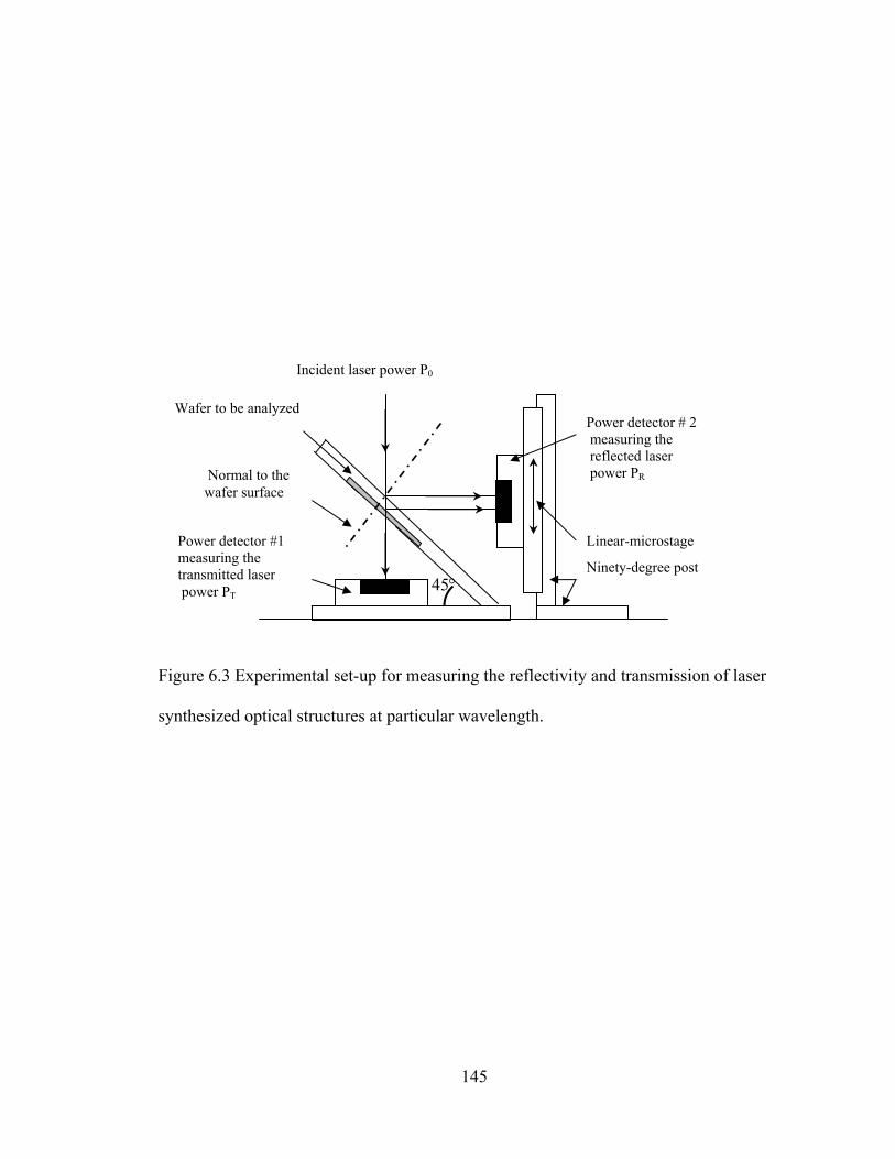
145
Figure 6.3 Experimental set-up for measuring the reflectivity and transmission of laser
synthesized optical structures at particular wavelength.
Wafer to be analyzed
Power detector #1 measuring the transmitted laser power PT
Power detector # 2 measuring the reflected laser power PR
Incident laser power P0
Normal to the wafer surface
Linear-microstage
Ninety-degree post 45°
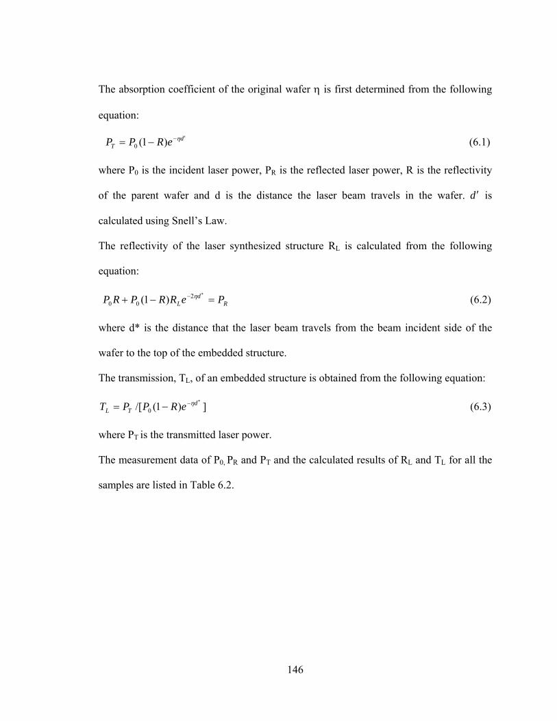
146
The absorption coefficient of the original wafer η is first determined from the following
equation:
dT eRPP ′−−= η)1(0 (6.1)
where P0 is the incident laser power, PR is the reflected laser power, R is the reflectivity
of the parent wafer and d is the distance the laser beam travels in the wafer. d ′ is
calculated using Snell’s Law.
The reflectivity of the laser synthesized structure RL is calculated from the following
equation:
Rd
L PeRRPRP =−+∗− η2
00 )1( (6.2)
where d* is the distance that the laser beam travels from the beam incident side of the
wafer to the top of the embedded structure.
The transmission, TL, of an embedded structure is obtained from the following equation:
])1(/[ 0
∗−−= dTL eRPPT η (6.3)
where PT is the transmitted laser power.
The measurement data of P0, PR and PT and the calculated results of RL and TL for all the
samples are listed in Table 6.2.

147
Table 6.2 Reflectivity and transmission calculation of laser synthesized optical structure
Parent wafer C rich phase C rich phase
containing N2
C rich phase
containing Al
P0 (mW) 1000 1000 1000 1000
PR (mW) 368 327 329 332
PT (mW) 390 53.3 51.0 56.0
η (cm-1) 6.07 - - -
d (μm)* 430 430 430 430
d ′ (μm) 450 450 450 450
d∗ (μm) ~ 450 ~ 450 ~ 450 ~ 450
RL (%) 20 27.3 27.7 28.2
TL (%) 60.5** 8.7 8.4 9.2
* d: Thickness of the original SiC substrate.
** Obtained from double face polished semi-insulating 6H-SiC wafer with the thickness
of 430 μm.

148
The calculated absorption coefficient of parent 6H-SiC, 6.07 cm-1 corresponds with the
data given in the reference [Goldberg et al (2001)]. The reflectivity of laser synthesized
embedded optical structures are increased by 40%; the parent wafer has a reflectivity of
20% and that for the laser synthesized structures are about 28% as shown in Fig. 6.4.
Accordingly the transmission of the laser synthesized optical structures decrease to about
9% compares to 60.5% of the parent wafer (Fig. 6.5).
16
18
20
22
24
26
28
30
32
C rich phaseC rich phasecontaining Al
C rich phasecontaining N2
Parentwafer
Ref
lect
ivity
(%)
Figure 6.4 Reflectivity of parent wafer, C rich phase, C rich phase containing N2 and C
rich phase containing Al measured at 1064 nm.

149
0
10
20
30
40
50
60
70
C rich phaseC rich phasecontaining Al
C rich phasecontaining N2
Parentwafer
Tran
smis
sion
%
Figure 6.5 Transmission of parent wafer, C rich phase, C rich phase containing N2 and C
rich phase containing Al measured at 1064 nm.

150
7 CHAPTER 7: SUMMARY
7.1 Conclusions
A novel laser direct metallization and doping technique is provided to direct metallize the
surface of silicon carbide without metal deposition and dope silicon carbide without high
temperature annealing in order to overcome some barriers in metallization and doping
during the fabrication of silicon carbide devices.
Laser irradiation of silicon carbide in a dopant-containing ambient allows to
simultaneously heating the silicon carbide surface and incorporating dopant atoms into
the silicon carbide lattice. Nitrogen and Trimethyaluminum (TMA) are used as dopants to
produce n-type and p-type doped silicon carbide, respectively. Two laser doping methods
are presented in this dissertation. i) Internal heating: Nd:YAG laser beam (λ=1064nm)
irradiates on the top polished surface of the silicon carbide wafer, but passing through the
bulk wafer, reaching the unpolished bottom surface and dopants are incorporated from
the bottom surface; ii): Excimer laser is used to irradiate the top surface of silicon carbide
wafer and dope the dopants simultaneously.
Laser internal heating doping method created a 800 nm n-type doped junction with a high
surface dopant concentration of 1×1021 cm-3 decreasing to 1.5 × 1019 cm-3 at the junction
and a 800 nm p-type doped junction with a surface dopant concentration of 5×1020 cm-3

151
decreasing to 1.5 × 1018 cm-3 at the junction based on laser enhanced solid phase
diffusion. Laser surface heating method produced p- type dopant depths of 200 nm and
450 nm for different numbers of laser pulses. For both types of lasers two diffusion
regions, near-surface region and far-surface region, were identified and two different
diffusion mechanisms are dominant in these two regions. The diffusion of dopant atoms
into the bulk silicon carbide can be explained by considering the laser-enhanced
substitutional and interstitial diffusion mechanisms. In the near-surface region, the dopant
atoms can easily diffuse into the bulk by occupying the vacancies created during the laser
irradiation process as well as interstitial sites. In the far-surface region the diffusion
process is dominated by the highly mobile interstitials. The effective diffusion
coefficients of nitrogen are 2.4 × 10⁻⁵ cm2/s for near-surface region and 9.2 × 10⁻⁶ cm2/s
for far-surface region; and those of aluminum are 1.2 × 10⁻⁵ cm2/s for near-surface region
and 1.3 × 10⁻⁶ cm2/s for far-surface. These values are 6 orders of magnitude higher than
the typical values of the diffusivity of nitrogen and aluminum in SiC. This indicates that
laser doping process enhances the diffusivity of dopants significantly.
Laser direct metallization can be realized on the surface of silicon carbide by generating
metal-like conductive phases due to the decomposition of silicon carbide. The laser
metallized contact can act as ohmic contact and it has been successfully used in the
fabrication of silicon carbide PIN diodes. Combination of laser direct metallization with
laser doping, i.e., fabricating laser direct metallized contacts on laser heavily doped SiC
substrate can dramatically improve the performance of such ohmic contact.

152
A pulsed laser-induced endolayer was fabricated on an n-type 6H-SiC substrate by
incorporating carbon based on laser solid-phase diffusion. Carbon atoms can be
incorporated into the top layer of silicon carbide substrates by excimer laser irradiation
using methane as a precursor. XEDS analysis shows the endolayer thickness to be 100
nm. TEM images show that there is no amorphization during the laser endotaxy process
and that the lattice structure of the endolayer remains undistorted compared to that of the
parent wafer, indicating the crystalline integrity of the endotaxy process. Rutherford
backscattering studies also show no amorphization and evident lattice disorder occur
during this laser solid phase diffusion process. In this study, the resistivity of the
endolayer is 1.1 ×10⁵ Ω·cm before annealing and 9.4 ×10⁴ Ω·cm after annealing at
1000°C for 10 min, which are high enough for many applications such as device
isolation.
Prototype silicon carbide PIN diodes have been fabricated on different silicon carbide
mediums, laser fabricated endolayer and parent epilayer on silicon carbide substrate,
using this laser doping technique and/or laser direct metallization. Results show that the
PIN diode fabricated on a 30 nm thick endolayer can block 18 V. High breakdown
voltages (420 ~ 500 V) and forward voltages drop at 100A/cm2 (12.5 ~ 20 V) have been
reached by laser doping and/or direct metallization fabricated PIN diodes on 4H-SiC with
a low doped homoepilayer, showing the effectiveness of the laser direct metallized
contact and the promise of this laser doping and direct metallization technique for the
fabrication of SiC PIN diodes compared to the PIN diodes fabricated by other techniques
such as epitaxial growth and ion implantation.

153
Embedded optical structures were also synthesized based on this laser direct metallization
technique. The increase of 40% reflectivity of the laser synthesized optical structures
compared to the parent wafer shows potential for the creation of optical, electro-optical,
opto-electrical, sensor devices and other integrated structures that are stable in high
temperature, high-pressure, corrosive environments and deep space applications.
7.2 Future Work
1) Experimental design for a dopant precursor delivery system that accounts for the
pyrophoric, and moisture sensitivity nature of some of the precursors such as
trimethylaluminum (TMAl) to control precisely the amount of dopant each fill and allows
the addition of more TMAl to the bubbler without exposure to the atmospheric moisture.
2) Transmission electron microscopy (TEM) and high resolution scanning electron
microscope (SEM) investigations should be utilized to study: (i) the crystal structure of
the laser-fabricated metal-like contacts. (ii)The orientation relationship between the
contact layer and the original wafer. (iii) The lattice defects at the interface between the
laser generated-track and the original Epilayer. (iv) Structural and compositional analysis
at the interfaces between laser doped, laser-metallized regions and the SiC wafer.
3) Investigating the impact of extended high temperature exposure in various ambients on
the stability of the laser generated contacts and diodes, endotaxial layers and optical
structures.

154
4) Dynamic characteristic of laser fabricated PIN diodes. More application of laser direct
metallization and doping technique on fabrication of silicon carbide devices such as LED
and optical filter.
5) Effect of laser induced vacancies on the diffusion coefficient. Mechanisms and
Characterization of laser induced vacancies.

155
REFERENCES
Alexandrov, P., Tone, K., Luo, Y., Zhao, J.H., Burke T., Pan M. and Weiner, M. (2001),
Electronics Letters, Vol. 37, pp. 531.
Alok, D., Baliga, B. J. and McLarty, P. K. (1994), A simple edge termination for silicon
carbide devices with nearly ideal breakdown voltage, IEEE Electron Device
Letters, 15, pp. 394-395.
Bäuerle, D. (2000), Laser Processing and Chemistry, 3rd. Edition, Springer-Verlag,
Berlin. pp. 103-107, 117-135.
Biserica, O., Godignon, P., Brezeanu, G., Badila M. and Rebollo, J. (2001), Design of a
reliable planar edge termination for SiC power devices, 2001 International
Semiconductor Conference. CAS 2001 Proceedings, Vol 2, pp. 353-356.
Bonchik, A. Yu., Kijak, S. G., Gotra, Z. and Proszak, W. (2001), Laser technology for
submicron-doped layers formation in semiconductors, Optics & Laser
Technology, Vol. 33, pp. 589-591.
Boulmer, J., Dragnea, B., Guedj, C., Debarre, D., Bosseboeuf, A., Finkman, E. and
Bourguignon, B. (1998), Laser-induced structural or compositional modifications
of Si or IV-IV surface: planarization, pulsed laser induced epitaxy, carbon
incorporation, and chemical etching Proceedings of the SPIE - The International
Society for Optical Engineering, V. 3404, pp. 149-158.
Boulmer, J. ; Boucaud, P.; Guedj, C.; Debarre, D.; Bouchier, D.; Finkman, E.; Prawer, S.;
Nugent, K.; Desmur-Larre, A.; Godet, C. and Cabarrocas, P. R. (1995),

156
Realization of Si1-x-yGexCy/Si heterostructures by pulsed laser induced epitaxy of
C implanted pseudomorphic SiGe films and of a-SiGeC:H films deposited on
Si(100), Journal of Crystal Growth, V. 157, pp. 436-441.
Bourdelle, K. K., Chechenin, N. G., Akhmanov, A. S.. Poroikov, A. Y. and Suvorov, A.
V. (1990), Melting and damage production in silicon carbide under pulse laser
irradiation, Physica Status Solidi A, Vol. 121, pp. 399-406.
Brown, W. L. (1983), Laser processing of semiconductors, in Laser Materials Processing,
edited by Bass M., North-Holland Publishing Company, Amsterdam, pp. 337-406.
Canut, B., Ramos, S., Roger, J. –A., Chante, J. –P., Locatelli, M. –L. and Planson, D.
(1997), Mater. Sci. Eng. B 46, 267
Carey, P. G., Weiner K. H. and Sigmon, T. W. (1988), A shallow junction submicrometer
PMOS process without high-temperature anneals, IEEE Electron Device Letters,.
Vol. 9, No. 10, pp. 542-544.
Casady, J. B. and Johnson, R. W. (1996), Status of silicon carbide (SiC) as a wide-
bandgap semiconductor for high-temperature applications: a review, Solid-State
Electronics, Vol. 39, pp. 1409-1422.
Chelnokov, V. E., Strel’chuk, A. M., Ivanov, P. A., Lentz G. and Parniere C. (1994), in
Proceedings of the 6th International Symposium on Power Semiconductor
Devices and ICs, pp.253 - 256
Chen, I. and Lee S. (1983), Transient temperature profiles in solids heated with a
scanning laser, Journal of Applied Physics, Vol. 54, pp.1062-1066.

157
Chou, S. Y., Chang, Y., Weiner, K. H., Sigmon, T. W. and Parsons, J. D. (1990),
Annealing of implantation damage and redistribution of impurities in SiC using a
pulsed excimer laser, Applied Physics Letter, Vol. 56(6), pp. 530-532.
Cline, H. E. and Anthony, T. R. (1977), Heat treating and melting material with a
scanning laser or electron beam, Journal of Applied Physics, Vol. 48, pp. 3895,-
3900.
Conde, J. C., Lusquiňos, F., González, P., León, B. and Pérez-Amor, M. (2002),
Temperature distribution in a material heated by laser radiation: modeling and
application, Vacuum, Vol. 64, pp. 359-366.
Constantinidis, G. (1997), Processing technologies for SiC, CAS '97 Proceedings., 1997
International Semiconductor Conference, Vol.1, pp. 161-170.
Dutto, C., Fogarassy, E., Mathiot, D., Muller, D., Kern, P. and Ballutaud, D. (2003),
Long-pulse duration excimer laser annealing of Al+ ion implanted 4H-SiC for pn
junction formation, Applied Surface Science, Vol. 208-209, pp. 292-297.
Dutto, C., Fogarassy, E. and Mathiot, D (2001), Numerical and experimental analysis of
pulsed excimer laser processing of silicon carbide, Applied Surface Science, Vol.
184, pp. 362-366.
Edwards, A., Dwight, D. N., Rao, M. V., Ridgway, M.C., Kelner, G., and Papanicolaou,
N. (1997), Compensation implants in 6H-SiC, Journal of Applied Physcis, Vol 82
(9), pp. 4223-4227.
Emorhokpor, E., Kerr, T., Zwieback, I., Elkington, W., Dudley, M., Anderson, T. and
Chen, J. (2004), Materials Research Society Symposium Proceedings, Vol.815,
pp.J5.19.1.

158
Eryu, O., Aoyama, K., Abe, K. and Nakashima, K. (2001), Impurity activation in N+ ion-
implanted 6H-SiC with pulsed laser annealing method, Materials Research Society
Symposium Proceedings, Vol. 640, pp. H5.31.1-H5.31.6.
Eryu, O., Kume, T., Nakashima, K., Nakata, T. and Inoue, M. (1997), Formation of an
ohmic electrode in SiC using a pulsed laser irradiation method, Nuclear
Instruments and Methods in Physics Research B, Vol 121, pp. 419-421.
Eryu, O., Okuyama, Y., Nakashima, K., Nakata, T. and Watanabe, M. (1995), Formation
of a p-n junction in silicon carbide by aluminum doping at room temperature using
a pulsed laser doping method, Applied Physics Letter, Vol 67 (14), pp. 2052-2053.
Fissel, A., Kaiser, U., Ducke, E., Schröter, B. and Richter, W. (1995), Epitaxial growth of
SiC thin films on Si-stabilized α-SiC (0001) at low temperatures by solid-source
molecular beam epitaxy, Journal of Crystal Growth, Vol. 154, pp. 72-80.
Fujihira, K., Tamura, S., Kimoto T. and Matsunami, H. (2002), Low-loss, high-voltage
6H-SiC epitaxial p-i-n diode, IEEE Transactions on electron device, Vol.49,
No.1, pp.150-154.
Fukada, S., Nakamura N., Monden, J. and Nishikawa, M. (2004), Experimental study of
cracking methane by Ni/SiO2 catalyst, Journal of Nuclear Materials, 329-333,
1365-1369.
Gadiyak, G. V. (1998), Theoretical model and computer simulation results of enhanced
diffusion of high-temperature implanted aluminum in silicon carbide, Nuclear
Instruments and Methods in Physics Research B, Vol.142, pp. 313-318.

159
Gamo, K., Murakami, K., Kawabe, M., Namba, S., and Aoyagi, Y. (1981), in Laser and
Electron Beam Solid Interactions and Materials Processing, eds,, Gibbons J.F.,
Hess, L.D. and Sigmon, T. W. (North-Holland, Amsterdam), pp. 97.
Giust, G. K. and Sigmon, T.W. (1997), Self-aligned aluminum top-gate polysilicon thin-
film transistors fabricated using laser recrystallization and gas-immersion laser
doping, IEEE Electron Device Letters, Vol.18 No. 8, pp. 394-396.
Goela, J. S., Pickering, M. A., Taylor, R. L. , Murray B. W. and Lompado, A. (1991)
Applied Optics, 30, 3166.
Goldberg Y, Levinshtein M, and Rumyantsev S (2001), Silicon Carbide (SiC), in:
Levinshtein ME, Rumayantsev SL and Shur MS, editors. Properties of Advanced
Semiconductor Materials, 1st Edition, New York: John Wiley & Sons, pp. 93-147.
Handy, E. M., Row, M. V., Holland, O. W., Chi, P. H., Jones, K. A., Derenge, M. A.,
Vispute, R. D. and Venkatesen, T. (2000), Al, B, and Ga ion-implantation doping
of SiC, Journal of Electronic Materials, Vol. 29, No. 11, p. 1340-1345
Harris, G. H. (1995), Properties of Silicon Carbide, Emis DATAREVIEW series No.13,
inspect publication, Exeter, England.
Heft, E. Wendler, T. Bachmann, Glaser, E.and Wesch, W. (1995), Defect production and
annealing in ion implanted silicon carbide, Materials Science and Engineering, B
29, pp. 142-146.
Itoh, A., Kimoto T. and Matsunami, H. (1996), Excellent reverse blocking characteristics
of high-voltage 4H-SiC Schottky rectifiers with boron-implanted edge
termination, IEEE Electron Device Letters, 17, 139-141.

160
Jones, E. C. and Ishida, E. (1998), Shallow junction doping technologies for ULSI,
Materials Science and Engineering R, Vol. 24, pp. 1-80.
Kaneda, S., Sakamoto, Y., Mihara, T., and Tanaka, T. (1987), Journal of Crystal Growth,
Vol. 81, pp. 536.
Kar, A., Scott, J. E. and Latham, W. P. (1996), Effects of mode structure on three-
dimensional laser heating due to single or multiple rectangular laser beams,
Journal of Applied Physics, Vol. 80, pp. 667-674.
Karmann, S., Suttrop, W., Schöner, A., Schadt, M., Haberstroh, C., Engelbrecht, F.,
Helbig, R., Pensl, G., Stein, R. A.and Leibenzeder, S. (1992),Chemical vapor
deposition and characterization of undoped and nitrogen-doped single crystalline
6H-SiC, Journal of Applied Physics, Vol. 72, pp. 5437-5442.
Kempshall, B. W., Giannuzzi, L. A., Prenitzer, B. I., Stevie F. A. and Da, S. X. (2002),
Comparative evaluation of protective coatings and focused ion beam chemical
vapor deposition processes, X. Journal of Vacuum Science Technology. B20, pp.
286-290.
Kern, R. S., Jarrendahl, K., Tanaka, S. and Davis, R. F. (1997), Homoepitaxial SiC
growth by molecular beam epitaxy, Physica Status Solidi (b), Vol. 202, pp. 379-
404.
Kerrien, G., Hernandez, M., Laviron, C., Sarnet, T., Debarre, D., Noguchi, T., Zahorski,
D., Venturini, J., Semeria, M. N. and Boulmer, J. (2003), Optical characterization
of laser processed ultra-shallow junctions, Applied Surface Science, Vol. 208-
209, pp. 277-284.

161
Kerrien, G., Sarnet, T., Debarre, D., Boulmer, J., Hernandez, M., Laviron, C., Semeria,
M. N. (2004), Gas immersion laser doping (GILD) for ultra-shallow junction
formation, Thin Solid Films, Vol. 453-454, pp. 106-109.
Kimerling, L. C. and Benton J. L. (1980), Defects in Laser-Processed Semiconductors.
In: White CW, Peercy PS, editors. Laser and Electron Beam Processing of
Materials, Academic, London, pp.385.
Kimto, T., Itoh, A. and Matsunami, H. (1997), Step-controlled epitaxial growth of high-
quality SiC layers, Physica Status Solidi, Vol. 202, pp. 247-260.
Konstantinov, A. O., Wahab, Q., Nordell N. and Lindefelt, U. (1997), Ionization rates
and critical fields in 4H silicon carbide, Applied Physics Letter, 71, pp. 90-92.
Kramer, K.M. and Thompson, M.O. (1996), Pulsed laser induced epitaxial crystallization
of carbon-silicon alloys, Journal of Applied Physics, V. 79, pp. 4118-4123.
Lipp, S., Frey, L., Lehrer, C., Frank, B., Demm E. and Ryssel, H. (1996), Investigations
on the topology of structures milled and etched by focused ion beams, Journal of
Vacuum Science Technology B14, pp. 3996-3999.
Levinshtein, M. E., Rumayantsev S. L. and Shur M. S. (2001), Properties of Advanced
Semiconductor materials, 1st Edition, John Wiley & Sons, New York, pp. 93.
Mahajan, S. and Sree Harsha, K. S. (1999), Principles of growth and processing of
semiconductors, McGraw-Hill Series in Materials Science and Engineering,
Boston, pp. 223-224.
Mazhukin, V. I., Smurov, I. and Flamant, G. (1995), Overheated metastable states in
pulsed laser action on ceramics, Journal of Applied Physics, Vol. 78, pp. 1259-
1270.

162
Mazumder J. and Kar, A. (1995), Theory and Application of Laser Chemical Vapor
Deposition, Plenum Press, New York. pp158.
Mohammad, F. A., Cao, Y. and Porter, L. M. (2005), Ohmic contacts to silicon carbide
determined by changes in the surface, Applied Physics Letters, Vol. 87, pp.
161908-1-161908-3.
Musumeci, P., Calcagno, L., Grimaldi, M.G. and Foti, G. (1996), Nuclear Instruments
and Methods. in Physics. Res. B Vol. 116, pp. 327.
Nadella, R.K and Capano, M.A. (1997), High-resistance layers in n-type 4H-silicon
carbide by hydrogen ion implantation, Applied Physics Letter, V. 70(7), pp. 886-
888.
Narushima, T.et al (1990), High-Temperature Oxidation of Chemical Vapor-Deposited
Silicon Carbide in Wet Oxygen at 1823-1923 K, Journal of American Ceramic
Society, Vol 73, pp. 3580-3584.
Neudeck, P. G. (2000), SiC Technology, VLSI Handbook, The Electrical Engineering
Hand Book Series, W. K. Chen, Ed. CRC press and IEEE press, Florida. pp. 6.1-
6.24.
Nordell, N. (2002), Bulk and epitaxial growth of SiC, in Process Technology for Silicon
Carbide Devices, edited by Carl-Mikael Zetterling, INSPEC, the Institution of
Electrical Engineers, London, pp.13-50.
Obreja, V. and Nuttall, K. (2002), Semiconductor Conference, 2002. CAS 2002
Proceedings. International , V2 , pp. 253.
Obreja, V. (2002), IEEE Transactions on Electron Device. 49 (1), pp. 155.

163
Pankove, J. I. (1999), GaN: from fundamental to applications, Materials Science and
Engineering B, Vol. 61-62, pp. 305-309.
Pantano, C. G. (1986), ASM Handbook Vol 10: Materials Characterization, ASM
International, USA, pp. 610.
Pearton, S. J. (2000), Processing of Wide Band Gap Semiconductors, 1 st. Edition
William Andrew publishing, New York.
Pensel, G., and Choyke, A. D. (1993), Electrical and optical characterization of silicon
carbide, Physica B: Condensed Matter, Vol. 185, pp.264-183.
Pokhmurska, A., Bonchik, O., Kiyak, S., Savitski G.and Gloskovsky A. (2000), Laser
doping in Si, InP and GaAs, Applied Surface Science, Vol. 154-155, pp. 712-715.
Porter, L., Davis, R. (1995), A critical review of ohmic and rectifying contacts for silicon
carbide. Materials Science & Engineering, B: Solid-State Materials for Advanced
Technology Vol. 34, No.(2-3), pp. 83-105
Quirk, M. and Serda, J. (2001), Semiconductor manufacturing technology, Prentice Hall.
Roccaforte, F., Via, F.L., Raineri, V., Pierobon, R.and Zanon E. (2003), Richardson’s
constant in inhomogeneous silicon carbide schottky contacts, Journal of Applied
Physics, Vol. 93, pp. 9137-9144.
Rupp, R., Lanig, P., Völkl, J. and Stephani, D. (1995) First results on silicon carbide
vapour phase epitaxy growth in a new type of vertical low pressure chemical
vapour deposition reactor, Journal of Crystal Growth, Vol. 146, 37-41.
Salama, I. A. (2003), Laser doping and metallization of wide bandgap materials: SiC,
GaN and AlN, Ph.D. Dissertation, University of Central Florida, Spring 2003.

164
Salama, I. A., Quick, N. R., Kar, A. (2002), Laser-fabricated metal-semiconductor
junctions on silicon carbide substrates, Proceedings of 21st International Congress
on Application of Lasers & Electro-Optics. pp.
Salama, I. A., Quick, N. R., Kar, A. (2003), Laser direct-metallization of silicon carbide
without metal deposition, Materials Research Society Symposium Proceedings,
Vol764, 75.
Salama, I. A., Middleton, C. F., Quick, N. R., Boreman, G. D. and Kar, A. (2003), Symp.
Nitride and Wide Bandgap Semiconductors for Sensors, Photonics and
Electronics IV, 204th meeting of the Electrochemical Society, Orlando, Florida,
October 12-16.
Salama, I. A., Quick, N. R., Kar, A. (2004), Laser direct writing and doping of diamond-
like carbon, polycrystalline diamond, and single crystal silicon carbide, Journal of
Laser Applications, Vol. 16, No. 2, pp. 92-99.
Scace, R. I. and Slack, G. A.(1959), Journal of physical Chemistry, Vol 30, pp.1551.
Schneider H. G. and Ruth V. (1976), Advances in Epitaxy and Endotaxy: Selected
chemical problems, Elsevier Scientific Publishing Company, New York, pp. 23-
78.
Schöner, A. (2002), Ion implantation and diffusion in SiC, in Process Technology for
Silicon Carbide Devices, edited by Carl-Mikael Zetterling, INSPEC, the
Institution of Electrical Engineers, London, pp. 51-84.
Schubert, E. F, (1993), Doping in III-V Semiconductors, Cambridge University Press,
Great British, pp. 354-391.

165
Sengupta, D. K., Quick, N. R. and Kar, A. (2001), Laser conversion of electrical
properties for silicon carbide device applications, Journal of Laser Applications,
Vol.13, No. 1, pp. 26-31.
Shalish, I. and Shapira, Y. (2000), Stability of schottky contacts with Ta-Si-N amorphous
diffusion barriers and overlayers on 6H-SiC, Journal of Vacuum Science and
Technology B, Vol.18, No.5, pp. 2477-2481.
Sharma, P. K., Rapp D. and Rahotgi N. K., (1999), Methane pyrolysis and disposing off
resulting carbon, (presented at In Situ Resource Utilization (ISRU III) Technical
Interchange Meeting, Denver, CO, 11-12 February 1999).
Singh, J. (2001), Semiconductor devices: basic principles, John Wiley & Sons Inc., New
York. pp. 146-149.
Singh, J. (1994), Semiconductor devices: an introduction, McGraw-Hill, New York, pp.
1.
Singh, R., Cooper, J. A., Melloch, M.R., Chow T. P. and Palmour, J.W. (2002), SiC
power schottky and PIN diodes, IEEE Transactions on electron device, Vol.49,
No.4, pp. 665-672.
Singh, R., Irvine, K. G., Capell, D. C., Richmond, J. T., Berning, D., Hefner A. R. and
Palmour J. W. (2002), IEEE Transactions on electron device, Vol. 49 p. 2308.
Solanki, R., Sudarsan, U. and Johnson, J. C. (1988), Laser-induced homoepitaxy of GaP,
Applied physics letter, V. 52 (11), pp. 919-921.
Speight, J. G. (2003), Perry’s Standard Tables and Formulas for Chemical Engineers,
McGRAW-HILL, New York. pp33.

166
Stringfellow, G. B. (1999), Organametallic Vapor-Phase Epitaxy: Theory and Practice,
Academic Press, San Diego, pp. 1-16.
Sugawara, Y., Takayama, D., Asano, K., Singh, R., Palmour, J. and Hayashi, T. (2001),
12-19 kV 4H-SiC pin diodes with low power loss, Procedings of 2001
International Sysposium on Power Semiconductor Devices & ICs, Osaka, pp. 27-
30.
Sze, S.M. (1981), Physics of Semiconductor Devices, John Wiley & Sons, New York,
pp.850.
Sze, S. M. (2001), Semiconductor devices, physics and technology, John Wiley & Sons,
New York, pp. 18.
Tajima, Y., Kijima, K., and Kingery, W. D. (1982), Diffusion of ion implanted aluminum
in silicon carbide, Journal of Chemical Physics, Vol 77, pp. 2592-2598.
Tanaka, Y., Tanoue, H. and Arai, K. (2003), Electrical activation of the ion-implanted
phosphorus in 4H-SiC by excimer laser annealing, Journal of Applied Physics,
Vol. 93, pp. 5934-5936.
Tian, Z., Quick, N. R., Kar, A. (2005), Effect of different laser sources and doping
methods used to dope silicon carbide, Acta Materialia, Vol. 53, pp. 2835- 2844.
Tian, Z., Quick, N. R., Kar, A. (2004), Laser direct write and gas immersion laser doping
fabrication of SiC diodes, Materials Research Society Symposium Proceedings,
Vol. 815, pp. J3.4-J3.9.
Tin, C. C, Madangarli, V., Luckowski, E., Casady, J., Isaacs-Smith, T., Williams, J.R.,
Johnson, R.W., Gradinaru G. and Sudarshan, T. S. (1996), Semiconductor

167
Electronics, 1996. ICSE '96. Proceedings, 1996 IEEE International Conference
on, pp. 55.
Tokarev, V. N. and Kaplan, A. F. (1999), An analytical modeling of time dependent
pulsed laser melting, Journal of Applied Physics, Vol. 86, pp. 2836-2846.
Troffer, T., Schadt, M., Frank, T. Itoh, H., Pensel, G., Heindi, J., Strunk, H, P. and
Maier, M. (1997), Doping of SiC by implantation of boron and aluminum.
Physica Status Solidi A: Applied Research, Vol. 162, No.1, pp.277-298.
Usov, I. O., Suvorova, A. A., Sokolov, V. V., Kudryavtsev, Y. A. and Suvorov, A. V.
(1999a), Transient enhanced diffusion of aluminum in SiC during high
temperature ion implantation, Journal of Applied Physics, Vol 86, pp. 6039-6042.
Usov, I. O., Suvorova, A. A., Sokolov, V. V., Kudryavtsev, Y. A. and Suvorov, A. V.
(1999b), Mechanism of enhanced diffusion of aluminum in 6H-SiC in the process
of high-temperature ion implantation, Materials Research Society Symposium
Proceeding 504, pp. 141-146.
Weiner, K. H., Carey, P. G., McCarthy A. M. and Sigmon, T. W. (1993), Microelectronic
Engineering, Vol. 20, pp.107-130.
Yoshida, S., Sakuma, E., Okumura, H., Misawa, S. and Endo, K. (1987), Heteroepitaxial
growth of SiC polytypes, Journal of Applied Physics, Vol. 62, pp. 303-305.
Zetterling, C. M. and östling, M. (2002), Advangtages of SiC, in Process Technology for
Silicon Carbide Devices, edited by Carl-Mikael Zetterling, INSPEC, the
Institution of Electrical Engineers, London, pp. 1-12.