Laser Lighting display and 3D Scanning
60
Laser Lighting display and 3D Scanning 6.111 Introductory Digital Systems Laboratory Shuyi Chen Gaston De Zarraga
Transcript of Laser Lighting display and 3D Scanning
Laser Lighting display and 3D Scanning
6.111 Introductory Digital Systems Laboratory
Shuyi Chen
Gaston De Zarraga

i
Abstract A multi functional laser projection/image processing system was implemented using FPGAs for digital signal control. In its current configuration the system is capable of tracing patterns with the laser using commands from a PS2 mouse that are stored in BRAM or generating swept planes of laser light and finding illuminated contours using filtered video data. The ultimate purpose of these functions is to extract 3-Dimensional spatial data from a target object. These systems would typically be very expensive, so we aim to achieve similar functionality on a much smaller budget.

ii
Table of Contents Overview 1 Description 2 Laser Projection (Gaston) 2 Labkit.v 2 Divider 2 PS/2 Mouse 4 Scan Sweep 4 Scan Control 5 Main Module 5 Trace Loop 5 BRAM 6 Reset BRAM 6 Divider: Loop Speed Control 6 Galvo Interface: External Hardware 6 Galvo Interface: Module 7 Testing & Debugging 8 Swept-Plane Scanner (James) 9 Camera Input 9 Hardware: NTSC Camera 9 ZBT RAM Access 9 Display 9 Top Level Module 10 Black and White Filter 11 Block Memory 11 Main Module 11 Noise Reduction 12 Line Detection 13 3D Point Extraction 14 Point Projection 15 Testing & Debugging 15 Conclusion 17 References 18 Appendices 19

iii
List of Figures Figure 1. Laser Projector Control Block Diagram 3
Figure 2. PS/2 Mouse Data Format 4
Figure 3. Laser Projector Hardware 7
Figure 4. TI – DAC 8871 Timing Diagram from Datasheet 8
Figure 5. Block Diagram of the Project 10
Figure 6. State Transition Diagram for the Main FSM 12
Figure 7. Method for Noise Reduction 13
Figure 8. Finding Mid-Point of Largest White Block 14
Figure 9. Depth Data Extraction 15

Page 1 of 56
Overview
The goals of this project is to explore the controlled projections of laser beams using high speed mirror galvanometers and construct a 3D laser swept-plane scanner with the result.
The projections are achieved by directing a laser beam onto one of the mirror galvanometers and then have it reflect onto the other one. By applying voltages into the galvanometers, the mirrors will rotate and in turn direct the laser beam. Voltage control was done by converting a serialized digital signal into a precise voltage value through a digital-to-analog converter. Point and click drawings can be made by storing position values in memory and have the galvanometers read from it. A laser swept-plane is produce by oscillating the vertical position galvanometer and slowly rotating the horizontal position galvanometer.
3D scanning with swept-plane works by analyzing 2D images produced during the scan and extract depth information based on controlled parameters. A simple swept-plane 3D scanner can be constructed using a point light source, a digital camera connected to a PC, and a thin rod to create shadows (lines) over the object being scanned. The conventional method is to have software programs analyze the data; this project aimed to reproduce the elements required for image processing and computation on an FPGA. In the end, elements of the scanner were synthesized but the scanner was not functional due to a lack of time to prepare the controlled parameters.

Page 2 of 56
Description Laser Projection (Gaston)
Labkit.v
Labkit.v is the outermost module of the system. Here is where all of the signals from the external peripherals are wired to the internal modules, as well as where the internal modules are instantiated and wired together. For the laser projection system, the user in/out ports were used to interface with the Digital to Analog Converters (DACs) for the mirror galvanometer controls, as well as with the laser diode and the separate image processing labkit. The PS/2 inout ports were used to communicate with a mouse peripheral which provides position and blanking commands for projection. The up, down, and enter buttons were debounced and used to trigger the state machines inside the scanning control system while two of the switches were wired to (1) control mode selection and (2) interrupt laser diode power while in trace projection mode. Additional outputs were wired from the labkit for debugging purposes; but they no longer serve any purpose.
Two TI-DAC8871's (one for each axis X-Y) were used to generate the voltage reference signals to command mirror angles and, therefore, laser position. From the user port output, the DACs shared three common and two independent signals. They shared an inverted 27 MHz clock signal (inverted because the DACs execute commands on the falling edge of the clock, while the rest of the system acts on the rising edge), an inverted reset signal (inverted because the DAC reset is active low), and the Chip Select signal. The other two user outputs to the DACs were data signals carrying the serialized 16-bit X and Y commands. One more user port output was used to power the laser diode directly. These signals were wired from the Galvo Interface module and will be discussed in greater detail in that section. The internal wiring of the labkit module is illustrated in the block diagram on the next page (Figure 1).
Divider
The divider module is a simple counter that increments an internal register every clock cycle and then resets while outputting a high command enable signal for one clock period. The command enable signal is asserted when the max count value has been reached. The max count and the required max count bits are parametrized so that the module can be reused for multiple timing signals by instantiating other dividers with different values. The default value for max count is 1350 with 11 count bits to enable 20,000 commands per second from a 27 MHz clock. These values were chosen to match the specified bandwidth of the galvanometer hardware.
Two slower dividers were also used in the system. One used a max count of 21600 with 15 count bits to control trace loop timing. This divider was necessary to extend the time between trace loop commands because the galvanometers could not perform large displacements at maximum bandwidth. The other divider served the same purpose but instead used the

Page 3 of 56
command enable signal as a clock and only counted to 16. This resulted in the same period but with the output enable signal lasting for 1350 clock cycles (ie. the period of command enable). This signal was used to generate the square wave to drive the fast vertical sweeping of the laser for the swept plane scan.
Figure 1. Laser Projector Control Block Diagram
Page 4 of 56
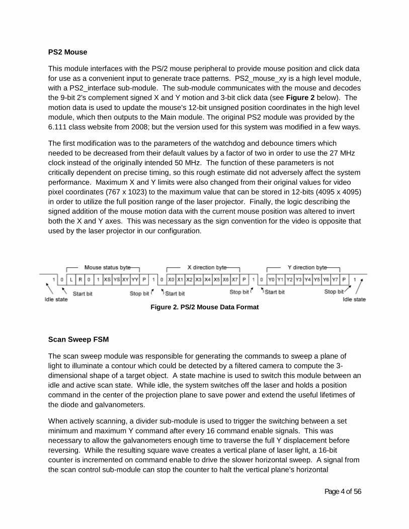
PS2 Mouse
This module interfaces with the PS/2 mouse peripheral to provide mouse position and click data for use as a convenient input to generate trace patterns. PS2_mouse_xy is a high level module, with a PS2_interface sub-module. The sub-module communicates with the mouse and decodes the 9-bit 2's complement signed X and Y motion and 3-bit click data (see Figure 2 below). The motion data is used to update the mouse's 12-bit unsigned position coordinates in the high level module, which then outputs to the Main module. The original PS2 module was provided by the 6.111 class website from 2008; but the version used for this system was modified in a few ways.
The first modification was to the parameters of the watchdog and debounce timers which needed to be decreased from their default values by a factor of two in order to use the 27 MHz clock instead of the originally intended 50 MHz. The function of these parameters is not critically dependent on precise timing, so this rough estimate did not adversely affect the system performance. Maximum X and Y limits were also changed from their original values for video pixel coordinates (767 x 1023) to the maximum value that can be stored in 12-bits (4095 x 4095) in order to utilize the full position range of the laser projector. Finally, the logic describing the signed addition of the mouse motion data with the current mouse position was altered to invert both the X and Y axes. This was necessary as the sign convention for the video is opposite that used by the laser projector in our configuration.
Figure 2. PS/2 Mouse Data Format
Scan Sweep FSM
The scan sweep module was responsible for generating the commands to sweep a plane of light to illuminate a contour which could be detected by a filtered camera to compute the 3-dimensional shape of a target object. A state machine is used to switch this module between an idle and active scan state. While idle, the system switches off the laser and holds a position command in the center of the projection plane to save power and extend the useful lifetimes of the diode and galvanometers.
When actively scanning, a divider sub-module is used to trigger the switching between a set minimum and maximum Y command after every 16 command enable signals. This was necessary to allow the galvanometers enough time to traverse the full Y displacement before reversing. While the resulting square wave creates a vertical plane of laser light, a 16-bit counter is incremented on command enable to drive the slower horizontal sweep. A signal from the scan control sub-module can stop the counter to halt the vertical plane's horizontal

Page 5 of 56
progression at 16 evenly divided intervals. If the sweep is not stopped, it takes approximately 3.5 seconds to travel 20° from right to left, due to the 16-bit counter (65535 max) being incremented 20K times per second. As long as the module remains in the active scan state, the vertical plane is continuously generated. Once the X command counter reaches its maximum, a scan complete register is set to one for one clock cycle, resetting the module to idle state.
Sub-Module: Scan Control
Scan control divides the horizontal sweep into 16 wedges by stopping the X command counter until an advance enable signal is received. These intervals allow the camera to average several frames of image data to filter out noise and find the illuminated contour. The advance enable signal is received through the user in/out port from the image processing labkit when it is ready to take another measurement.
The sub-module works by using a 5-bit register to keep count of how many advance enable signals have been received. If the X command counter is less than the 16-bit number composed of the advance_enable counter value as the 5 MSB followed by 11 bits of 1, a signal is sent to the scan sweep FSM allowing the count to continue incrementing. Otherwise, the count is stopped. The scan complete or reset signal resets the scan control to its initial state.
Main Module
MainFSM.v is a misleading file name because the main module is not itself an FSM; but contains an FSM sub-module, Trace Loop. The main module simply routes the scan sweep or the trace loop signals to the galvo interface, depending on the position of switch 0. The scan sweep commands are already 16 bits, so they are passed as they are; but the loop trace commands are only 12-bits wide so they are passed to the output as the 12 most significant command bits followed by 4 bits of 0. The main module also wires the position and button click data signals from the PS/2 mouse module to the trace loop sub-module to store in BRAM.
Sub-Module: Trace Loop
Trace loop is responsible for: (1) storing position and blanking commands generated from the mouse input to BRAM and (2) reading back all of the previously stored commands in a continuous loop to trace the recorded pattern with the laser beam. The proper function of this sub-module depends on three other sub-modules below it: a BRAM, reset BRAM, and a divider. They will be discussed in the following sub-sections.
The trace loop reads memory at the address value of a counter which is incremented by the loop enable signal from the divider. When the counter reaches the current highest address, trace loop writes the current mouse position to the BRAM, signals the laser diode to illuminate the mouse cursor, and resets the address loop counter. If a mouse button is clicked, the loop
Page 6 of 56
trace will wait until BRAM is not being accessed (the vast majority of clock time is open) and increment the current highest address value. If the left button is clicked, a register will store a bit telling the laser diode to turn on. If the right button is clicked, the register will store a command to turn the diode off. The next time the loop address counter reaches the current highest address, loop trace will write the mouse coordinates and the laser signal register value to the highest current address before it increments. The data values coming from the BRAM are wired out to the main module, where they are directed to the galvo interface module.
Sub-Sub-Module: BRAM
The mybram.v file provided for lab 4a was used for the BRAM sub-module. It is instantiated in trace loop with 7 address bits and a bit width of 25. The first 12 bits store the recorded mouse X position, the next 12, the Y position, and the final bit stores the laser command. When a new address is selected, the data at that location is output on the next clock cycle. If write enable is asserted, the current data input is loaded into the currently selected address and then output on the next clock cycle. This one cycle delay from address request to data output is accounted for in the design of the trace loop module.
Sub-Sub-Module: Reset BRAM
This sub-module is a finite state machine with the sole purpose of pausing the trace loop and then clearing all memory addresses. Upon receiving the reset signal, an output register signals the divider and trace loop to reset to their initial states and wait until the register returns to 0. While this reset hold register contains a 1, the reset BRAM sub-module increments every clock cycle through every address and writes zeros. When all addresses have been cleared, the reset hold is released allowing the system to function as usual.
Sub-Sub-Module: Divider
This divider was already discussed in the general divider section.
Galvo Interface: External Hardware
The mirror galvanometers are driven by an external 24V DC power supply through separate closed loop PID controllers to achieve high speed and precision. These driver cards accept reference position commands in the form of an analog voltage differential signal, which could not be supplied directly by the labkit. This necessitated the use of digital-to-analog converters with another external supply to provide +/- 15V for power which was also reduced to +/- 10V reference using a voltage divider stabilized with OpAmps. Two Texas Instruments DAC 8871 chips were used to control the analog signaling to the galvanometer drivers. The DAC 8871

Page 7 of 56
accepts 16-bit serial data input which must be timed with a chip select signal to ensure that data is not corrupted. The timing of these signals is show below in Figure 3. The external hardware can also be seen in the picture below.
Figure 3. Laser Projector Hardware
Galvo Interface: Module
The galvanometer interface module is responsible for communicating position commands to the DACs and timing the laser blanking signal to coincide with the pointing command. This module uses a state machine that serializes the command signals. While idle, the chip select signal is held at 1 and the transmission complete register is reset to 0. Upon receiving the command enable signal from the divider, the module enters the transmission state and copies the current

Page 8 of 56
X and Y commands to two 16-bit registers to be serialized. Once in the transmission state, chip select is held at 0 and the values of each bit are transmitted in order from most to least significant while a counter keeps track of how many bits have been sent. As the last bit is being sent, galvo interface outputs the laser blanking signal and returns to the idle state, setting chip select back to 1 signaling the DACs to load the 16 previously received bits. The timing diagram below (Figure 4) illustrates the sequence of events.
Figure 4. TI - DAC 8871 timing diagram from datasheet
Testing and Debugging
Debugging the laser projection system required the use of all of the available tools. During testing, certain parts of the system did not initially behave as expected and it was only when all of debugging data was compared that the source of the problems could be determined. For example, when we had first connected the mouse input directly to the galvo interface and started measuring DAC voltage output on the oscilloscope, everything appeared to work except that the voltage would sometimes flip if the mouse was moved too far. At first, we thought the problem was caused by the mouse coordinates overflowing and jumping to the other extreme. When we observed the mouse coordinates on the hex display, it was obvious that they were not overflowing and the mouse module was not the source of the problem. This hypothesis was further undermined by the fact that the same behavior was observed in the horizontal scan sweep. Upon wiring up the galvo interface outputs to the logic analyzer, the problem revealed itself. The chip select signal was asserted for one too many clock cycles, causing the most significant bit to be cut off and the overflow that was being observed in the second most significant bit.
Another bug that was particularly troublesome involved the loop trace module. This bug was particularly subtle because the system, at first, appeared to behave correctly. At this point, the system could record commands from the mouse and trace patterns; but for some reason the performance of the system would change depending on how many commands were currently

Page 9 of 56
stored in the BRAM. The first couple of points would be traced correctly; but once another was added the straight lines traced by the laser would become warped. A few more clicks and it would normal again, but add another and the points would start being connected out of order or only one point would appear. The source of the problem was pinpointed using the logic analyzer on the trace loop module. The divider that was being used to increment the memory loop was only supposed to assert loop enable for once clock cycle every 16 command enable signals. We had mistakenly used the same type of divider that had worked in the scan sweep to control the flipping of the Y command. In that divider, command enable is used as a clock signal and the enable signal asserts for one cycle of whatever is being used as a clock. In the case of the command enable clock, the dividers enable output is asserted for 1350 27MHz clock cycles. This was causing the loop trace module to loop continuously while loop enable remained asserted. The dependence of the behavior on the number stored points was the result of beat patterns. The loop was incrementing once per clock cycle and then being cutoff at unexpected values, causing the galvos to jump to whichever value was currently being read the moment command enable was asserted.
Swept-Plane Scanner (James)
Camera Input (video_decoder.v)
Hardware: NTSC Camera
After the adv7185init module is run at start up, NTSC signals transmitted by the camera is decoded into digital signals in YCbCr color space. The NTSC decoder module was written by a 6.111 course staff to demonstrate the functions of the ZBT memories.
ZBT RAM Access (zbt_6111.v, ntsc2zbt.v)
The zbt_6111.v module provides an interface for the Labkit to communicate with the on-board ZBT memories, and the ntsc2zbt.v module takes and stores the 8-bit grayscale values that are derived from the NTSC signal into the ZBT memory. The modules were provided by the 6.111 course staff. The ntsc2zbt.v module was slightly modified to move the window of video frame to the upper left corner.
Display (vram_display.v, xvga.v)
Display is driven by the signals produced by the xvga.v module; it is used to produce a display of 1024 pixel by 768 pixel at 60 Hz. The pixel values of the display are the grayscale values stored in ZBT memory through the ntsc2zbt.v module. These modules were provided by the 6.111 course staff to assist us in our projects.

Page 10 of 56
Top Level Module (Labkit.v)
This module is provided by the 6.111 course to interface with our Labkits. Labkit.v handles all the inputs and outputs on the actual Labkit. This version of labkit.v contains codes that were written by past course staff; in particular, the NTSC camera input, ZBT RAM access, the VGA display output, and all the relevant wirings were all done in 2005.
The relevant code snippets in this module were modified to allow access of the second ZBT RAM; modules written for this project were all instantiated within this top level module. Communication between the main_fsm.v module and the galvanometers will also take place this module. A block diagram of the project is shown in figure 5.
Figure 5: Block diagram of the project
External Display
(To all modules)
Clock_65
mhz
Reset
NTSC Camera
Switch [7:4]
Scan_complete Switch[0]
Advance_en

Page 11 of 56
James - Black and White Filter (bwfilter.v)
Inputs: [7:0] pixel_in, [7:0] threshold;
Outputs: [7:0] pixel_out;
We intended to perform scanning in a dark environment; the high contrast between the object surface and the laser reflection would allow more accurate edge detection and line data extraction. This simple module will process an 8-bit grayscale pixel input and compare it with a threshold value. Any input pixel with values less than the threshold will be converted to a black pixel with grayscale value 8’b0000_0000; and any input with values greater than the threshold will be converted into a white pixel (grayscale value 8’b1111_1111). The input values are connected to the pixels generated by the vram_display.v module, and the output is send as pixels for external display. The threshold input is connected to external switches to allow run-time contrast adjustment.
Block Memory (mybram.v)
This module was provided by the 6.111 course staff to create block memories (BRAMs) used for store information on the FPGA.
James – Main Module (main_fsm.v)
Inputs: clk, reset, scan_on, comp15_done, ld_done, scan_complete;
Outputs: advance_en, comp15_en, ld_enable, save_en;
The main module acts as a controller for image processing and 3D data extraction; its purpose is to communicate with Gaston’s Labkit and activate the relevant sub-modules in order. Once the module is activated, it will command Gaston’s Labkit to advance the laser line in steps across the object being scanned. The division between each step can be customized by Gaston on his Labkit. Between each step, modules compare15.v, line_det.v, and point3d_zbt.v are activated in order to process the still shot and save the 3D data extracted into ZBT RAM. Once the main module processes every shot, it will activate the module that displays the 2D projection of the 3D points out on VGA monitor. Regrettably, the display module was not implemented successfully; and once the imaging processing finishes, the main module returns to its reset state. Figure 6 on the next page shows the state transition diagram for the main finite state machine.
The main module implements a finite state machine (FSM) to control each components of the image processing. At power on, the main module starts in the reset state. Once the signal scan_on is asserted, in addition to sending mirror advance signals (advance_en) to Gaston’s Labkit, the FSM will also activate the point3d_zbt.v module to start processing line data and storing the extracted 3D coordinates into the second ZBT RAM . The scan_on signal is wired to

Page 12 of 56
the first switch on the Labkit; the FSM will not return to its reset state unless the switch is turned off or the scan_complete signal is asserted from Gaston’s Labkit. After every mirror advance signal, the FSM first asserts high on comp15_en to activate the compare15.v module; after the module finishes storing the stabilized/noise-reduced frame data into the BRAM, it asserts the comp15_done signal to transition the FSM into its line detecting state.
Figure 6: State transition diagram for the main FSM
Once arrived at the line detecting state, the compare15.v module will deactivate and ld_enable is asserted to activate the line detection module (line_det.v). Line_det.v works concurrently with point3d_zbt.v. Similar to the previous step, once line_det.v is finished processing, it asserts the ld_done signal to the FSM, making it transition into its Scan On state. The FSM asserts the advance_en signal to Gaston’s Labkit, and the process repeats. The FSM will only go back to its reset state when the switch controlling the scan_on signal is turned off or when it receives a high scan_complete signal asserted by Gaston’s Labkit when the galvanometer finishes its sweep.
James - Noise Reduction (compare15.v)
Inputs: clk, reset, comp15_en, bwpixel, [10:0] hcount, [9:0] vcount;
Outputs: comp15_done, bram_we, bram_data, [18:0] bram_addr;

Page 13 of 56
The information sent from the digital camera contains noise; for a still shot, the noise presents itself as pixels with varying values. This effect can be observed even in a dark scanning environment, especially around the edges of the laser line. In order to stabilize the image for line detection, this module will process a still shot 15 times for each pixel and count the number of occurrences of white pixels. If the count at the end of the 15 frames is greater than a threshold value, the module assigns that pixel white, otherwise, the module assigns that pixel black. The threshold value is set to ten initially, and can be changed as needed. The method is shown is figure 7.
Figure 7: when count reaches 15, if count_white is greater than a threshold value, the pixel will be saved as white.
The module starts in the reset state; when the main module (main_fsm.v) asserts an enable signal (comp15_en), pixel processing will start from the upper left corner of the shot and work its way to the lower right, using hcount and vcount values as identifiers for individual pixels. To allow line detection, this module will save the output pixel values into a BRAM (an instance of the mybram.v module): value 1’b0 for black pixels and value 1’b1 for white pixels. The BRAM addresses used to store the output pixel values are determined by hcount and vcount values; using these values reduces the amount of data stored because they are system wide signals produced by the xvga.v module. When the module reaches the end of the shot, and all the relevant pixels has been processed, it transitions into reset state and asserts a signal back to the main module to initiate line detection.
James - Line Detection (line_det.v)
Inputs: clk, reset, ld_enable, bram_read;
Outputs: ld_done, line_pt_valid, [18:0] bram_addr, [9:0] x, [8:0] y;
To properly extract the 3D data from scanning, we will need to analyze every shot that contains the laser line. After a still shot containing the laser line gets processed by the compare15.v module, we will be able to access the result in the aforementioned BRAM. By this stage, pixel values have been stabilized, and the resulting image in BRAM will consist of minimal noise. The solid vertical line in question will have a horizontal thickness; this module checks each horizontal line for a block of white pixels, and at the end of the line, the midpoint of the thickest
Page 14 of 56
white block (horizontal slice of the line) is computed and its coordinate is passed into the module that extracts 3D data from line data.
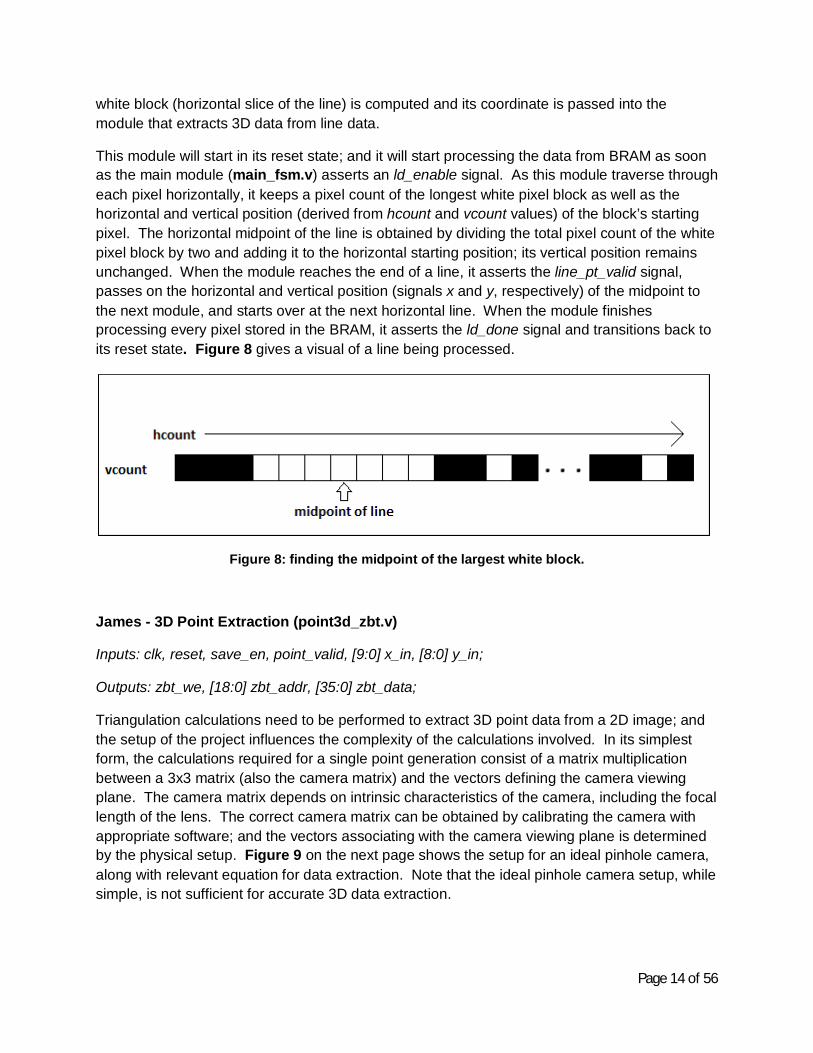
This module will start in its reset state; and it will start processing the data from BRAM as soon as the main module (main_fsm.v) asserts an ld_enable signal. As this module traverse through each pixel horizontally, it keeps a pixel count of the longest white pixel block as well as the horizontal and vertical position (derived from hcount and vcount values) of the block’s starting pixel. The horizontal midpoint of the line is obtained by dividing the total pixel count of the white pixel block by two and adding it to the horizontal starting position; its vertical position remains unchanged. When the module reaches the end of a line, it asserts the line_pt_valid signal, passes on the horizontal and vertical position (signals x and y, respectively) of the midpoint to the next module, and starts over at the next horizontal line. When the module finishes processing every pixel stored in the BRAM, it asserts the ld_done signal and transitions back to its reset state. Figure 8 gives a visual of a line being processed.
Figure 8: finding the midpoint of the largest white block.
James - 3D Point Extraction (point3d_zbt.v)
Inputs: clk, reset, save_en, point_valid, [9:0] x_in, [8:0] y_in;
Outputs: zbt_we, [18:0] zbt_addr, [35:0] zbt_data;
Triangulation calculations need to be performed to extract 3D point data from a 2D image; and the setup of the project influences the complexity of the calculations involved. In its simplest form, the calculations required for a single point generation consist of a matrix multiplication between a 3x3 matrix (also the camera matrix) and the vectors defining the camera viewing plane. The camera matrix depends on intrinsic characteristics of the camera, including the focal length of the lens. The correct camera matrix can be obtained by calibrating the camera with appropriate software; and the vectors associating with the camera viewing plane is determined by the physical setup. Figure 9 on the next page shows the setup for an ideal pinhole camera, along with relevant equation for data extraction. Note that the ideal pinhole camera setup, while simple, is not sufficient for accurate 3D data extraction.

Page 15 of 56
Figure 9: depth data extraction. [1]
This module will start in its reset state. Once the main module (main_fsm.v) asserts the save_en signal high, this module transitions and stays out of reset state until the save_en signal asserts low. Once out of reset state, this module will stay in the state of standby while monitoring the x-y coordinate inputs coming from the line detection module (line_det.v); as soon as the line detection module finishes processing one horizontal line, it asserts the line_pt_valid signal to initiate calculation in this module. The x-y coordinates will be processed and used (in combination with camera matrix specified by the parameter values) to determine the 3D coordinate of that point. The module then asserts the write enable signal for ZBT memory (zbt_we) and stores the coordinate values of that point into ZBT RAM. The data stored will be the concatenation of three 12-bit registers, each holding values for an axis in 3D space ({x,y,z}); the address will increment by 1 for every coordinate data stored. Once the main module is finished scanning and processing, it will assert signal save_en low, and the 3D extraction module will go back to its reset state. In the mean time, the points stored in ZBT RAM can be accessed for display.
James – Point Projection (Unfinished)
This module was originally planned; however, time and implementation constraints prevented the completion of the module. This module was intended to display a 2D projection of the 3D point cloud stored in ZBT RAM. An alternative solution would be to have the Labkit interface with a computer through the RS232 port, and send the coordinate data to MATLAB for display.
Testing and Debugging
During initial testing, where a threshold value of 100 was chosen for the black and white filter, the image quality resulting from the filter was too poor for proper processing. Since the lighting condition under which the scan is to be taken place can vary, external switches are wired into the filter for better run-time customization.
The noise reducing module (compare15.v) aims to remove flickering pixels by comparing 15 frames of the same shot and determining the resulting pixel using a threshold value. Different thresholds were used to determine the optimal value. Testing started with a threshold value of 10; no further improvements were found by increasing the threshold value.
Page 16 of 56
A bug was initially found in the line detection module (line_det.v) that prevents it from storing the values necessary to calculate the midpoint of the largest white block on a horizontal line; after rewriting the module from scratch, we are confident that the bug is fixed. Unfortunately, the new module was not tested prior to the completion of this paper, and therefore it remains uncertain whether the module is working properly.
The first version of the 3D data extraction module (point3d_zbt.v) had timing issues regarding information storage on the ZBT RAM; holding the address, data, and the write enable signals for 1 cycle was not sufficient to guaranteed a successful write (may be due to a skewed clock). As a result, the module now holds the values for 3 cycles before transitioning back to its standby state.
Due to timing and technical constraints, a calibration was not done on the camera; in addition, the scanning mechanism was not properly set up. Without the necessary parameter, the 3D data extraction module would not be able to determine coordinates with any accuracy. The placeholder parameters defined within the module describe a camera matrix under for an ideal pinhole camera; they are to be changed in accordance with the calibration and setup data. Depending on the complexity, pipelining the multiplications may be necessary.
Optimization of the codes is usually performed after the codes are proven functional; since the project was not completed in time, optimization was not done. The current code relies on slow scanning speed; in the future, the main FSM will be modified to perform faster image processing.

Page 17 of 56
Conclusion
We started this project knowing that it would have a large scope and that we probably wouldn't get all the functionality that we originally wanted out of our system; but we also chose this project because the intermediate steps towards our reach goal of a fully functional 3-D laser scanner, would still be presentable accomplishments. With that said, we are quite pleased with our results. The mouse controlled laser projector function worked flawlessly after thorough debugging and testing and the scanning function of the laser combined with our image data filters proved to be viable for a 3D laser scanner, even if we couldn't finish the spatial data extraction and plotting modules on time.
Given the initial hurdle of figuring out and wiring up the analog electronics for the DACs combined with the unexpected setback of losing several days worth of progress to a lab computer hard drive crash, we still managed to make most of our milestones towards the final goal. Though it may not be relevant for a digital systems lab, we also gained some valuable experience working with the analog circuitry for this project. Debugging for this project also provided a lot of useful insights into good Verilog coding practices which is certainly a valuable take away.
Having already made this much progress towards our desired 3D scanner, we've decided to invest in a Nexsys2 prototyping board so that we can finish the project over IAP. Due to the many potential applications of high speed precision laser control, we also plan to experiment with new functions. For example, with some relatively simple extensions to our current laser control system we can make projected video games such as pong. We can also add a computer interface to download ILDA format laser show files and to upload image data for processing in MATLAB.

Page 18 of 56
References
[1] Lanman, Douglas, and Taubin, Gabriel, “Build Your Own 3D Scanner: 3D Photography for Beginners,” Pg. 19, Fig. 2.7, 2009.

Page 19 of 56
Appendice
A. Labkit.v (Gaston)
`default_nettype none /////////////////////////////////////////////////////////////////////////////// // // 6.111 FPGA Labkit -- Template Toplevel Module // // For Labkit Revision 004 // Created: October 31, 2004, from revision 003 file // Author: Nathan Ickes, 6.111 staff // /////////////////////////////////////////////////////////////////////////////// module labkit( // Remove comment from any signals you use in your design! // AC97 /* output wire beep, audio_reset_b, ac97_synch, ac97_sdata_out, input wire ac97_bit_clock, ac97_sdata_in, */ // VGA /* output wire [7:0] vga_out_red, vga_out_green, vga_out_blue, output wire vga_out_sync_b, vga_out_blank_b, vga_out_pixel_clock, vga_out_hsync, vga_out_vsync, */ // NTSC OUT /* output wire [9:0] tv_out_ycrcb, output wire tv_out_reset_b, tv_out_clock, tv_out_i2c_clock, tv_out_i2c_data, output wire tv_out_pal_ntsc, tv_out_hsync_b, tv_out_vsync_b, tv_out_blank_b, output wire tv_out_subcar_reset; */ // NTSC IN /* input wire [19:0] tv_in_ycrcb, input wire tv_in_data_valid, tv_in_line_clock1, tv_in_line_clock2, tv_in_aef, tv_in_hff, tv_in_aff, output wire tv_in_i2c_clock, tv_in_fifo_read, tv_in_fifo_clock, tv_in_iso, tv_in_reset_b, tv_in_clock, inout wire tv_in_i2c_data, */ // ZBT RAMS /* inout wire [35:0] ram0_data, output wire [18:0] ram0_address, output wire ram0_adv_ld, ram0_clk, ram0_cen_b, ram0_ce_b, ram0_oe_b, ram0_we_b, output wire [3:0] ram0_bwe_b, inout wire [35:0]ram1_data, output wire [18:0]ram1_address, output wire ram1_adv_ld, ram1_clk, ram1_cen_b, ram1_ce_b, ram1_oe_b, ram1_we_b, output wire [3:0] ram1_bwe_b, input wire clock_feedback_in, output wire clock_feedback_out, */ // FLASH /*

Page 20 of 56
inout wire [15:0] flash_data, output wire [23:0] flash_address, output wire flash_ce_b, flash_oe_b, flash_we_b, flash_reset_b, flash_byte_b, input wire flash_sts, */ // RS232 /* output wire rs232_txd, rs232_rts, input wire rs232_rxd, rs232_cts, */ // PS2 inout wire mouse_clock, mouse_data, //input wire keyboard_clock, keyboard_data, // FLUORESCENT DISPLAY output wire disp_blank, disp_clock, disp_rs, disp_ce_b, disp_reset_b, input wire disp_data_in, output wire disp_data_out, // SYSTEM ACE /* inout wire [15:0] systemace_data, output wire [6:0] systemace_address, output wire systemace_ce_b, systemace_we_b, systemace_oe_b, input wire systemace_irq, systemace_mpbrdy, */ // BUTTONS, SWITCHES, LEDS //input wire button0, //input wire button1, //input wire button2, //input wire button3, input wire button_enter, //input wire button_right, //input wire button_left, input wire button_down, input wire button_up, input wire [7:0] switch, output wire [7:0] led, // USER CONNECTORS, DAUGHTER CARD, LOGIC ANALYZER //inout wire [31:0] user1, //inout wire [31:0] user2, inout wire [31:0] user3, //inout wire [31:0] user4, //inout wire [43:0] daughtercard, output wire [15:0] analyzer1_data, output wire analyzer1_clock, //output wire [15:0] analyzer2_data, output wire analyzer2_clock, //output wire [15:0] analyzer3_data, output wire analyzer3_clock, //output wire [15:0] analyzer4_data, output wire analyzer4_clock, // CLOCKS //input wire clock1, //input wire clock2, input wire clock_27mhz ); wire command_enable; wire reset; wire [15:0] X_command; wire [15:0] Y_command; wire X_sdi; wire Y_sdi; wire CS; wire [15:0] scanX, scanY; wire [11:0] mx, my; wire [2:0] btn_click; wire laser, laserS, laserT;

Page 21 of 56
wire [63:0] data; wire [4:0] address, loop_addr, current_addr; wire write_enable, loop_enable, advance_enable, scan_complete; //////////////////////////////////////////////////////////////////////////// // // Reset Generation // // A shift register primitive is used to generate an active-high reset // signal that remains high for 16 clock cycles after configuration finishes // and the FPGA's internal clocks begin toggling. // //////////////////////////////////////////////////////////////////////////// wire reset_init; SRL16 reset_sr(.D(1'b0), .CLK(clock_27mhz), .Q(reset_init), .A0(1'b1), .A1(1'b1), .A2(1'b1), .A3(1'b1)); defparam reset_sr.INIT = 16'hFFFF; wire button_ent_debounced; debounce db_ent(reset, clock_27mhz, button_enter, button_ent_debounced); wire button_down_debounced; debounce db_down(reset, clock_27mhz, button_down, button_down_debounced); wire button_up_debounced; debounce db_up(reset, clock_27mhz, button_up, button_up_debounced); assign reset = reset_init | ~button_ent_debounced; assign user3[0] = ~clock_27mhz; assign user3[1] = X_sdi; assign user3[2] = Y_sdi; assign user3[3] = CS; assign user3[4] = ~reset; assign user3[5] = laser; assign advance_enable = user3[6]; assign user3[7] = scan_complete; assign user3[31:8] = 0; assign led[7:3] = 5'b11111; assign led[2:0] = ~btn_click; assign data[63:28] = {switch[7:2],35'h0}; assign data[27:16] = mx; assign data[15:12] = 4'b0000; assign data[11:0] = my; assign analyzer1_clock = clock_27mhz; assign analyzer1_data[4:0] = address; assign analyzer1_data[8:5] = loop_addr; assign analyzer1_data[12:9] = current_addr; assign analyzer1_data[13] = write_enable; assign analyzer1_data[14] = command_enable; assign analyzer1_data[15] = btn_click[2]; MainFSM Main(.clk(clock_27mhz), .reset(reset), .command_enable(command_enable), .mode_select(switch[0]), .mx(mx), .my(my), .btn_click(btn_click), .scanX_in(scanX), .scanY_in(scanY), .X_command(X_command), .Y_command(Y_command), .laser(laserT), .address(address), .loop_addr(loop_addr), .current_addr(current_addr), .write_enable(write_enable), .loop_enable(loop_enable)); divider pps20K(.clk(clock_27mhz),.reset(reset),.command_enable(command_enable)); scan_sweep sweep(.clk(clock_27mhz), .reset(reset), .down(~button_down_debounced), .command_enable(command_enable), .advance_enable(advance_enable), .X_command(scanX), .Y_command(scanY), .laser(laserS), .scan_complete(scan_complete));

Page 22 of 56
ps2_mouse_xy mouse_in(.clk(clock_27mhz), .reset(reset), .ps2_clk(mouse_clock), .ps2_data(mouse_data), .mx(mx), .my(my), .btn_click(btn_click)); Galvo_Interface GI(.clk(clock_27mhz), .command_enable(command_enable), .X_command_in(X_command), .Y_command_in(Y_command), .laser_in((switch[1] & laserT) | laserS), .X_command_out(X_sdi), .Y_command_out(Y_sdi), .laser_out(laser), .CS(CS)); display_16hex debug(reset, clock_27mhz, data, disp_blank, disp_clock, disp_rs, disp_ce_b, disp_reset_b, disp_data_out); endmodule
B. Divider.v module divider #(parameter MAX_COUNT = 1350, COUNT_BITS = 11)(input clk, reset, output reg command_enable); reg [COUNT_BITS-1:0] count; always@(posedge clk) begin //increment counter each rising clock edge count <= count + 1; //reset counter if(reset) count <= 0; //output command_enable and reset counter every 1350 rising clock edges (for 20Kpps) if(count == MAX_COUNT) begin command_enable <= 1; count <= 0; end else command_enable <= 0; end endmodule
C. Ps2_mouse.v //Modified slightly by Gaston de Zarraga // ps2_mouse_xy gives a high-level interface to the mouse, which // keeps track of the "absolute" x,y position (within a parameterized // range) and also returns button presses. module ps2_mouse_xy(clk, reset, ps2_clk, ps2_data, mx, my, btn_click); input clk, reset; inout ps2_clk, ps2_data; // data to/from PS/2 mouse output [11:0] mx, my; // current mouse position, 12 bits output [2:0] btn_click; // button click: Left-Middle-Right // module parameters // parameter MAX_X = 1023; // parameter MAX_Y = 767; parameter MAX_X = 4095; //Max value storeable in 12 bits parameter MAX_Y = 4095; // for use with laser projector // low level mouse driver

Page 23 of 56
wire [8:0] dx, dy; wire [2:0] btn_click; wire data_ready; wire error_no_ack; wire [1:0] ovf_xy; wire streaming; // original 6.111 fall 2005 Verilog - appears to be buggy so it has been // commented out. // ps2_mouse m1(clk,reset,ps2_clk,ps2_data,dx,dy,ovf_xy, btn_click, // data_ready,streaming); // // using ps2_mouse Verilog from Opencore // divide the clk by a factor of two sot that it works with 65mhz and the original timing // parameters in the open core source. // if the Verilog doesn't work the user should update the timing parameters. This Verilog assumes // 50Mhz clock; seems to work with 32.5mhz without problems. GPH 11/23/2008 with // assist from BG ps2_mouse_interface #(.WATCHDOG_TIMER_VALUE_PP(13000), //timer values halved for 27Mhz clock .WATCHDOG_TIMER_BITS_PP(14), .DEBOUNCE_TIMER_VALUE_PP(123), .DEBOUNCE_TIMER_BITS_PP(7)) m1( .clk(clk), .reset(reset), .ps2_clk(ps2_clk), .ps2_data(ps2_data), .x_increment(dx), .y_increment(dy), .data_ready(data_ready), .read(1'b1), // force a read .left_button(btn_click[2]), .right_button(btn_click[0]) // rx_read_o ); // error_no_ack not used // Update "absolute" position of mouse reg [11:0] mx, my; wire sx = dx[8]; // signs wire sy = dy[8]; wire [8:0] ndx = sx ? {0,~dx[7:0]}+1 : {0,dx[7:0]}; // magnitudes wire [8:0] ndy = sy ? {0,~dy[7:0]}+1 : {0,dy[7:0]}; always @(posedge clk) begin mx <= reset ? MAX_X/2 : //This X is for video cursor // data_ready ? (sx ? (mx>ndx ? mx - ndx : 0) // : (mx < MAX_X - ndx ? mx+ndx : MAX_X)) : mx; //This X is for laser cursor data_ready ? (sx ? (mx < MAX_X - ndx ? mx+ndx : MAX_X) : (mx>ndx ? mx - ndx : 0)) : mx; // note Y is flipped for video cursor use of mouse my <= reset ? MAX_Y/2 : // data_ready ? (sy ? (my < MAX_Y - ndy ? my+ndy : MAX_Y) // : (my>ndy ? my - ndy : 0)) : my; //Y not flipped for laser cursor mouse

Page 24 of 56
data_ready ? (sy ? (my>ndy ? my - ndy : 0) : (my < MAX_Y - ndy ? my+ndy : MAX_Y)) : my; end endmodule //------------------------------------------------------------------------------------- // // Author: John Clayton // Date : April 30, 2001 // Update: 6/06/01 copied this file from ps2.v (pared down). // Update: 6/07/01 Finished initial coding efforts. // Update: 6/09/01 Made minor changes to state machines during debugging. // Fixed errors in state transitions. Added state to m2 // so that "reset" causes the mouse to be initialized. // Removed debug port. // // // // // // Description //------------------------------------------------------------------------------------- // This is a state-machine driven serial-to-parallel and parallel-to-serial // interface to the ps2 style mouse. The state diagram for part of the // m2 state machine was obtained from the work of Rob Chapman, as published // at: // www.ee.ualberta.ca/~elliott/ee552/studentAppNotes/1998_w/mouse_notes.html // // // Some aspects of the mouse interface are not implemented (e.g, verifying // the FA response code from the mouse when enabling streaming mode.) // However, the mouse interface was designed so that "hot plugging" a mouse // into the connector should cause the interface to send the F4 code to the // mouse in order to enable streaming. By this means, the mouse begins to // operate, and no reset pulse should be needed. // // Similarly, there is a "watchdog" timer implemented, so that during periods // of inactivity, the bit_count is cleared to zero. Therefore, the effects of // a bad count value are corrected, and internal errors of that type are not // propagated into subsequent packet receive operations. // // To enable the streaming mode, F4 is sent to the mouse. // The mouse responds with FA to acknowledge the command, and then enters // streaming mode at the default rate of 100 packets per second (transmission // of packets ceases when the activity at the mouse is not longer sensed.) // // There are additional commands to change the sampling rate and resolution // of the mouse reported data. Those commands are not implemented here. // (E8,XX = set resolution 0,1,2,3) // (E7 = set scaling 2:1) // (E6 = reset scaling) // (F3,XX = set sampling rate to XX packets per second.) // // At this time I do not know any of the command related to using the // wheel of a "wheel mouse." // // The packets consists of three bytes transmitted in sequence. The interval // between these bytes has been measured on two different mice, and found to // be different. On the slower (older) mouse it was approximately 345 // microseconds, while on a newer "wheel" mouse it was approximately 125 // microseconds. The watchdog timer is designed to cause processing of a // complete packet when it expires. Therefore, the watchdog timer must last // for longer than the "inter-byte delay" between bytes of the packet. // I have set the default timer value to 400 usec, for my 49.152 MHz clock. // The timer value and size of the timer counter is settable by parameters, // so that other clock frequencies and settings may be used. The setting for // the watchdog timeout is not critical -- it only needs to be greater than // the inter-byte delay as data is transmitted from the mouse, and no less // than 60usec. //
Page 25 of 56
// Each "byte" of the packet is transmitted from the mouse as follows: // // 1 start bit, 8 data bits, 1 odd parity bit, 1 stop bit. == 11 bits total. // (The data bits are sent LSB first) // // The data bits are formatted as follows: // // byte 0: YV, XV, YS, XS, 1, 0, R, L // byte 1: X7..X0 // byte 2: Y7..Y0 // // Where YV, XV are set to indicate overflow conditions. // XS, YS are set to indicate negative quantities (sign bits). // R, L are set to indicate buttons pressed, left and right. // // // // The interface to the ps2 mouse (like the keyboard) uses clock rates of // 30-40 kHz, dependent upon the mouse itself. The mouse generates the // clock. // The rate at which the state machine runs should be at least twice the // rate of the ps2_clk, so that the states can accurately follow the clock // signal itself. Four times oversampling is better. Say 200kHz at least. // In order to run the state machine extremely fast, synchronizing flip-flops // have been added to the ps2_clk and ps2_data inputs of the state machine. // This avoids poor performance related to slow transitions of the inputs. // // Because this is a bi-directional interface, while reading from the mouse // the ps2_clk and ps2_data lines are used as inputs. While writing to the // mouse, however (which is done when a "packet" of less than 33 bits is // received), both the ps2_clk and ps2_data lines are sometime pulled low by // this interface. As such, they are bidirectional, and pullups are used to // return them to the "high" state, whenever the drivers are set to the // high impedance state. // // Pullups MUST BE USED on the ps2_clk and ps2_data lines for this design, // whether they be internal to an FPGA I/O pad, or externally placed. // If internal pullups are used, they may be fairly weak, causing bounces // due to crosstalk, etc. There is a "debounce timer" implemented in order // to eliminate erroneous state transitions which would occur based on bounce. // Parameters are provided to configure the debounce timer for different // clock frequencies. 2 or 3 microseconds of debounce should be plenty. // You may possibly use much less, if your pullups are strong. // // A parameters is provided to configure a 60 microsecond period used while // transmitting to the mouse. The 60 microsecond period is guaranteed to be // more than one period of the ps2_clk signal. // // //------------------------------------------------------------------------------------- `resetall `timescale 1ns/100ps `define TOTAL_BITS 33 // Number of bits in one full packet module ps2_mouse_interface ( clk, reset, ps2_clk, ps2_data, left_button, right_button, x_increment, y_increment, data_ready, // rx_read_o read, // rx_read_ack_i error_no_ack );
Page 26 of 56
// Parameters // The timer value can be up to (2^bits) inclusive. parameter WATCHDOG_TIMER_VALUE_PP = 10800; // Number of sys_clks for 400usec. parameter WATCHDOG_TIMER_BITS_PP = 14; // Number of bits needed for timer parameter DEBOUNCE_TIMER_VALUE_PP = 93; // Number of sys_clks for debounce parameter DEBOUNCE_TIMER_BITS_PP = 7; // Number of bits needed for timer // State encodings, provided as parameters // for flexibility to the one instantiating the module. // In general, the default values need not be changed. // There are three state machines: m1, m2 and m3. // States chosen as "default" states upon power-up and configuration: // "m1_clk_h" // "m2_wait" // "m3_data_ready_ack" parameter m1_clk_h = 0; parameter m1_falling_edge = 1; parameter m1_falling_wait = 3; parameter m1_clk_l = 2; parameter m1_rising_edge = 6; parameter m1_rising_wait = 4; parameter m2_reset = 14; parameter m2_wait = 0; parameter m2_gather = 1; parameter m2_verify = 3; parameter m2_use = 2; parameter m2_hold_clk_l = 6; parameter m2_data_low_1 = 4; parameter m2_data_high_1 = 5; parameter m2_data_low_2 = 7; parameter m2_data_high_2 = 8; parameter m2_data_low_3 = 9; parameter m2_data_high_3 = 11; parameter m2_error_no_ack = 15; parameter m2_await_response = 10; parameter m3_data_ready = 1; parameter m3_data_ready_ack = 0; // I/O declarations input clk; input reset; inout ps2_clk; inout ps2_data; output left_button; output right_button; output [8:0] x_increment; output [8:0] y_increment; output data_ready; input read; output error_no_ack; reg left_button; reg right_button; reg [8:0] x_increment; reg [8:0] y_increment; reg data_ready; reg error_no_ack; // Internal signal declarations wire watchdog_timer_done; wire debounce_timer_done; wire packet_good; reg [`TOTAL_BITS-1:0] q; // Shift register
Page 27 of 56
reg [2:0] m1_state; reg [2:0] m1_next_state; reg [3:0] m2_state; reg [3:0] m2_next_state; reg m3_state; reg m3_next_state; reg [5:0] bit_count; // Bit counter reg [WATCHDOG_TIMER_BITS_PP-1:0] watchdog_timer_count; reg [DEBOUNCE_TIMER_BITS_PP-1:0] debounce_timer_count; reg ps2_clk_hi_z; // Without keyboard, high Z equals 1 due to pullups. reg ps2_data_hi_z; // Without keyboard, high Z equals 1 due to pullups. reg clean_clk; // Debounced output from m1, follows ps2_clk. reg rising_edge; // Output from m1 state machine. reg falling_edge; // Output from m1 state machine. reg output_strobe; // Latches data data into the output registers //-------------------------------------------------------------------------- // Module code assign ps2_clk = ps2_clk_hi_z?1'bZ:1'b0; assign ps2_data = ps2_data_hi_z?1'bZ:1'b0; // State register always @(posedge clk) begin : m1_state_register if (reset) m1_state <= m1_clk_h; else m1_state <= m1_next_state; end // State transition logic always @(m1_state or ps2_clk or debounce_timer_done or watchdog_timer_done ) begin : m1_state_logic // Output signals default to this value, unless changed in a state condition. clean_clk <= 0; rising_edge <= 0; falling_edge <= 0; case (m1_state) m1_clk_h : begin clean_clk <= 1; if (~ps2_clk) m1_next_state <= m1_falling_edge; else m1_next_state <= m1_clk_h; end m1_falling_edge : begin falling_edge <= 1; m1_next_state <= m1_falling_wait; end m1_falling_wait : begin if (debounce_timer_done) m1_next_state <= m1_clk_l; else m1_next_state <= m1_falling_wait; end m1_clk_l : begin if (ps2_clk) m1_next_state <= m1_rising_edge; else m1_next_state <= m1_clk_l; end m1_rising_edge : begin rising_edge <= 1;
Page 28 of 56
m1_next_state <= m1_rising_wait; end m1_rising_wait : begin clean_clk <= 1; if (debounce_timer_done) m1_next_state <= m1_clk_h; else m1_next_state <= m1_rising_wait; end default : m1_next_state <= m1_clk_h; endcase end // State register always @(posedge clk) begin : m2_state_register if (reset) m2_state <= m2_reset; else m2_state <= m2_next_state; end // State transition logic always @(m2_state or q or falling_edge or rising_edge or watchdog_timer_done or bit_count or packet_good or ps2_data or clean_clk ) begin : m2_state_logic // Output signals default to this value, unless changed in a state condition. ps2_clk_hi_z <= 1; ps2_data_hi_z <= 1; error_no_ack <= 0; output_strobe <= 0; case (m2_state) m2_reset : // After reset, sends command to mouse. begin m2_next_state <= m2_hold_clk_l; end m2_wait : begin if (falling_edge) m2_next_state <= m2_gather; else m2_next_state <= m2_wait; end m2_gather : begin if (watchdog_timer_done && (bit_count == `TOTAL_BITS)) m2_next_state <= m2_verify; else if (watchdog_timer_done && (bit_count < `TOTAL_BITS)) m2_next_state <= m2_hold_clk_l; else m2_next_state <= m2_gather; end m2_verify : begin if (packet_good) m2_next_state <= m2_use; else m2_next_state <= m2_wait; end m2_use : begin output_strobe <= 1;
Page 29 of 56
m2_next_state <= m2_wait; end // The following sequence of 9 states is designed to transmit the // "enable streaming mode" command to the mouse, and then await the // response from the mouse. Upon completion of this operation, the // receive shift register contains 22 bits of data which are "invalid" // therefore, the m2_verify state will fail to validate the data, and // control will be passed into the m2_wait state once again (but the // mouse will then be enabled, and valid data packets will ensue whenever // there is activity on the mouse.) m2_hold_clk_l : begin ps2_clk_hi_z <= 0; // This starts the watchdog timer! if (watchdog_timer_done && ~clean_clk) m2_next_state <= m2_data_low_1; else m2_next_state <= m2_hold_clk_l; end m2_data_low_1 : begin ps2_data_hi_z <= 0; // Forms start bit, d[0] and d[1] if (rising_edge && (bit_count == 3)) m2_next_state <= m2_data_high_1; else m2_next_state <= m2_data_low_1; end m2_data_high_1 : begin ps2_data_hi_z <= 1; // Forms d[2] if (rising_edge && (bit_count == 4)) m2_next_state <= m2_data_low_2; else m2_next_state <= m2_data_high_1; end m2_data_low_2 : begin ps2_data_hi_z <= 0; // Forms d[3] if (rising_edge && (bit_count == 5)) m2_next_state <= m2_data_high_2; else m2_next_state <= m2_data_low_2; end m2_data_high_2 : begin ps2_data_hi_z <= 1; // Forms d[4],d[5],d[6],d[7] if (rising_edge && (bit_count == 9)) m2_next_state <= m2_data_low_3; else m2_next_state <= m2_data_high_2; end m2_data_low_3 : begin ps2_data_hi_z <= 0; // Forms parity bit if (rising_edge) m2_next_state <= m2_data_high_3; else m2_next_state <= m2_data_low_3; end m2_data_high_3 : begin ps2_data_hi_z <= 1; // Allow mouse to pull low (ack pulse) if (falling_edge && ps2_data) m2_next_state <= m2_error_no_ack; else if (falling_edge && ~ps2_data) m2_next_state <= m2_await_response; else m2_next_state <= m2_data_high_3; end m2_error_no_ack : begin error_no_ack <= 1; m2_next_state <= m2_error_no_ack; end

Page 30 of 56
// In order to "cleanly" exit the setting of the mouse into "streaming" // data mode, the state machine should wait for a long enough time to // ensure the FA response is done being sent by the mouse. Unfortunately, // this is tough to figure out, since the watchdog timeout might be longer // or shorter depending upon the user. If the watchdog timeout is set to // a small enough value (less than about 560 usec?) then the bit_count // will get reset to zero by the watchdog before the FA response is // received. In that case, bit_count will be 11. // If the bit_count is not reset by the watchdog, then the // total bit_count will be 22. // In either case, when this state is reached, the watchdog timer is still // running and it is best to let it expire before returning to normal // operation. One easy way to do this is to check for the bit_count to // reach 22 (which it will always do when receiving a normal packet) and // then jump to "verify" which will always fail for that time. m2_await_response : begin if (bit_count == 22) m2_next_state <= m2_verify; else m2_next_state <= m2_await_response; end default : m2_next_state <= m2_wait; endcase end // State register always @(posedge clk) begin : m3_state_register if (reset) m3_state <= m3_data_ready_ack; else m3_state <= m3_next_state; end // State transition logic always @(m3_state or output_strobe or read) begin : m3_state_logic case (m3_state) m3_data_ready_ack: begin data_ready <= 1'b0; if (output_strobe) m3_next_state <= m3_data_ready; else m3_next_state <= m3_data_ready_ack; end m3_data_ready: begin data_ready <= 1'b1; if (read) m3_next_state <= m3_data_ready_ack; else m3_next_state <= m3_data_ready; end default : m3_next_state <= m3_data_ready_ack; endcase end // This is the bit counter always @(posedge clk) begin if (reset) bit_count <= 0; // normal reset else if (falling_edge) bit_count <= bit_count + 1; else if (watchdog_timer_done) bit_count <= 0; // rx watchdog timer reset end // This is the shift register always @(posedge clk) begin if (reset) q <= 0; else if (falling_edge) q <= {ps2_data,q[`TOTAL_BITS-1:1]}; end // This is the watchdog timer counter

Page 31 of 56
// The watchdog timer is always "enabled" to operate. always @(posedge clk) begin if (reset || rising_edge || falling_edge) watchdog_timer_count <= 0; else if (~watchdog_timer_done) watchdog_timer_count <= watchdog_timer_count + 1; end assign watchdog_timer_done = (watchdog_timer_count==WATCHDOG_TIMER_VALUE_PP-1); // This is the debounce timer counter always @(posedge clk) begin if (reset || falling_edge || rising_edge) debounce_timer_count <= 0; // else if (~debounce_timer_done) else debounce_timer_count <= debounce_timer_count + 1; end assign debounce_timer_done = (debounce_timer_count==DEBOUNCE_TIMER_VALUE_PP-1); // This is the logic to verify that a received data packet is "valid" // or good. assign packet_good = ( (q[0] == 0) && (q[10] == 1) && (q[11] == 0) && (q[21] == 1) && (q[22] == 0) && (q[32] == 1) && (q[9] == ~^q[8:1]) // odd parity bit && (q[20] == ~^q[19:12]) // odd parity bit && (q[31] == ~^q[30:23]) // odd parity bit ); // Output the special scan code flags, the scan code and the ascii always @(posedge clk) begin if (reset) begin left_button <= 0; right_button <= 0; x_increment <= 0; y_increment <= 0; end else if (output_strobe) begin left_button <= q[1]; right_button <= q[2]; x_increment <= {q[5],q[19:12]}; y_increment <= {q[6],q[30:23]}; end end endmodule //`undefine TOTAL_BITS
D. Scan_sweep.v `timescale 1ns / 1ps ////////////////////////////////////////////////////////////////////////////////// // Company: // Engineer: // // Create Date: 13:44:41 11/23/2010 // Design Name: // Module Name: scan_sweep // Project Name: // Target Devices:
Page 32 of 56
// Tool versions: // Description: // // Dependencies: // // Revision: // Revision 0.01 - File Created // Additional Comments: // ////////////////////////////////////////////////////////////////////////////////// module scan_sweep(clk, reset, down, command_enable, advance_enable, X_command, Y_command, laser, scan_complete); input clk, reset, down, command_enable, advance_enable; output reg [15:0] X_command, Y_command; output reg laser, scan_complete; reg [15:0] count; reg state, next_state, flip; wire flip_enable, advanceX; parameter IDLE = 0; parameter SCAN = 1; //Scan control allows other labkit to halt horizontal sweep to take more measurements scan_control EighthRangeIncrement(.clk(clk), .reset(reset), .state(state), .scan_complete(scan_complete) ,.advanceX_command(advance_enable), .countX(count), .advanceX(advanceX)); //Divider to give Y time to track high amplitude square wave divider #(.MAX_COUNT(15), .COUNT_BITS(4)) divY(.clk(command_enable), .reset(reset), .command_enable(flip_enable)); always@(posedge clk) begin state <= next_state; if(reset) begin //reload initial values count <= 0; scan_complete <= 0; flip <= 0; laser <= 0; end if(state == IDLE) begin //Hold these values if not doing anything count <= 0; scan_complete <= 0; flip <= 0; X_command <= 16'b1000000000000000; Y_command <= 16'b1000000000000000; laser <= 0; end if(state == SCAN) begin laser <= 1; //turn laser diode on for duration of scan sweep if(command_enable && advanceX) count <= count + 1; //increment counter every command enable if advanceX allows if(flip_enable) flip <= ~flip; //Trigger Y command flip to make vertical laser plane X_command <= count[15:0]; if(flip) Y_command <= 16'b1110000000000000; //Y command High else Y_command <= 16'b0010000000000000; //Y command low if(count === 65534) scan_complete <= 1; //End scan end end always@* begin //Trigger state transitions case(state) IDLE: next_state <= (down)? SCAN: IDLE; SCAN: next_state <= (reset)? IDLE: (scan_complete)? IDLE: SCAN; endcase end endmodule

Page 33 of 56
E. Scan_control.v
`timescale 1ns / 1ps ////////////////////////////////////////////////////////////////////////////////// // This module stops the horizontal sweep at 16 intervals and waits for a signal // allow sweep to proceed to next stopping point. Allows image processing labkit // to take more measurements before the scan completes. ////////////////////////////////////////////////////////////////////////////////// module scan_control(clk, reset, state, scan_complete, advanceX_command, countX, advanceX); input clk, reset, state, advanceX_command, scan_complete; input [15:0] countX; output reg advanceX; reg temphold; reg [4:0] advanceCount; always@(posedge clk) begin if(reset || scan_complete) advanceCount <= 4'b0000; //Increment counter if in scan mode and enable signal received from outside if(advanceX_command && state) advanceCount <= advanceCount + 1; //use this when signal comes from other labkit // if(advanceX_command) temphold <= 1; //use this if button is being used to signal // if(!advanceX_command && temphold) begin // advanceCount <= advanceCount + 1; // temphold <= 0; // end //Allow count to proceed until stopping point has been reached if(countX < {advanceCount, 11'b111111111111}) advanceX <= 1; //Stop count else advanceX <= 0; //Old unnecessary code /* case(advanceCount) 4'b0000: begin if(countX < {16'b0000111111111111}) advanceX <= 1; else advanceX <= 0; end 4'b0001: begin if(countX < 16'b0001111111111111) advanceX <= 1; else advanceX <= 0; end 4'b0010: begin if(countX < 16'b0010111111111111) advanceX <= 1; else advanceX <= 0; end 4'b0011: begin if(countX < 16'b0011111111111111) advanceX <= 1; else advanceX <= 0; end 4'b0100: begin if(countX < 16'b0100111111111111) advanceX <= 1; else advanceX <= 0; end 4'b0101: begin if(countX < 16'b0101111111111111) advanceX <= 1; else advanceX <= 0; end 4'b0110: begin

Page 34 of 56
if(countX < 16'b0110111111111111) advanceX <= 1; else advanceX <= 0; end 4'b0111: begin if(countX < 16'b0111111111111111) advanceX <= 1; else advanceX <= 0; end 4'b1000: begin if(countX < 16'b1000111111111111) advanceX <= 1; else advanceX <= 0; end 4'b1001: begin if(countX < 16'b1001111111111111) advanceX <= 1; else advanceX <= 0; end 4'b1010: begin if(countX < 16'b1010111111111111) advanceX <= 1; else advanceX <= 0; end 4'b1011: begin if(countX < 16'b1011111111111111) advanceX <= 1; else advanceX <= 0; end 4'b1100: begin if(countX < 16'b1100111111111111) advanceX <= 1; else advanceX <= 0; end 4'b1101: begin if(countX < 16'b1101111111111111) advanceX <= 1; else advanceX <= 0; end 4'b1110: begin if(countX < 16'b1110111111111111) advanceX <= 1; else advanceX <= 0; end 4'b1111: begin if(countX < 16'b1111111111111111) advanceX <= 1; else advanceX <= 0; end endcase */ end endmodule
F. MainFSM.v `timescale 1ns / 1ps ////////////////////////////////////////////////////////////////////////////////// // Company: // Engineer: // // Create Date: 17:30:48 11/18/2010 // Design Name: // Module Name: MainFSM // Project Name: // Target Devices: // Tool versions: // Description:

Page 35 of 56
// // Dependencies: // // Revision: // Revision 0.01 - File Created // Additional Comments: // ////////////////////////////////////////////////////////////////////////////////// module MainFSM(clk, reset, command_enable, mode_select, mx, my, btn_click, scanX_in, scanY_in, X_command, Y_command, laser, address, loop_addr, current_addr, write_enable, loop_enable); input clk, command_enable, reset; input [11:0] mx, my; input [2:0] btn_click; input [15:0] scanX_in, scanY_in; input mode_select; output reg [15:0] X_command, Y_command; output wire laser, write_enable, loop_enable; output wire [6:0] address, loop_addr, current_addr; parameter Mouse = 0; parameter Scan = 1; wire [11:0] TraceX, TraceY; //Trace loop contains BRAM that stores and loops through mouse command history to trace desired patterns Trace_Loop #(.LOGSIZE(7))Draw(.clk(clk), .reset(reset), .command_enable(command_enable), .mx(mx), .my(my), .btn_click(btn_click), .X_out(TraceX), .Y_out(TraceY), .laser(laser), .address(address), .loop_addr(loop_addr), .current_addr(current_addr), .write_enable(write_enable), .loop_enable(loop_enable)); always@(posedge clk) begin if(mode_select == Mouse) begin X_command <= {TraceX,4'b0000}; //DACs have 16-bit resolution; but we only need 12 Y_command <= {TraceY,4'b0000}; //so the 4 least significant bits are set to 0 end if(mode_select == Scan) begin X_command <= scanX_in; Y_command <= scanY_in; end end endmodule
G. Trace_loop.v (with resetBRAM) `timescale 1ns / 1ps ////////////////////////////////////////////////////////////////////////////////// // Company: // Engineer: // // Create Date: 14:06:04 12/06/2010 // Design Name: // Module Name: Trace_Loop // Project Name: // Target Devices: // Tool versions: // Description: // // Dependencies: // // Revision: // Revision 0.01 - File Created // Additional Comments: // //////////////////////////////////////////////////////////////////////////////////

Page 36 of 56
module Trace_Loop #(parameter LOGSIZE = 7)(clk, reset, command_enable, mx, my, btn_click, X_out, Y_out, laser, address, loop_addr, current_addr, write_enable, loop_enable); input clk, reset, command_enable; input [11:0] mx, my; input [2:0] btn_click; output reg [11:0] X_out, Y_out; output reg laser; output reg [LOGSIZE-1:0] address = 0; output reg [LOGSIZE-1:0] loop_addr = 0; output reg [LOGSIZE-1:0] current_addr = 0; reg [24:0] data_in; wire [24:0] data_out; output wire loop_enable; output reg write_enable; reg Lclick_hold = 0; reg Rclick_hold = 0; reg laserReg; wire resetHold; wire [LOGSIZE-1:0] addressCLEAR; //reg [5:0] max_count = 16; //BRAM module to store mouse data and read command command loop from mybram #(.LOGSIZE(LOGSIZE), .WIDTH(25)) Trace_Mem(.addr(address), .clk(clk), .din(data_in), .dout(data_out), .we(write_enable)); //Module with sole purpose of clearing all addresses in BRAM resetBRAM #(.LOGSIZE(LOGSIZE)) clearTRACE(.clk(clk), .reset(reset), .resetHold(resetHold), .addressCLEAR(addressCLEAR)); //Experimental module for future improvements //variable_divider #(.COUNT_BITS(5)) LoopSpeedControl(.clk(command_enable), .reset(resetHold), // .max_count(max_count), .enable(loop_enable)); //Divider to extend time between loop commands enough for galvos to follow divider #(.MAX_COUNT(21600), .COUNT_BITS(15)) LoopSpeedControl(.clk(clk), .reset(resetHold), .command_enable(loop_enable)); always@(posedge clk) begin //Hold system in starting configuration while resetBRAM clears memory if(resetHold) begin current_addr <= 0; loop_addr <= 0; address <= addressCLEAR; write_enable <= 1; //Hold write enable so that resetBRAM can overwrite with zeros data_in <= 25'd0; //Hold zeros to overwrite memory data Lclick_hold <= 0; Rclick_hold <= 0; laserReg <= 1; //max_count <= 16; end if(btn_click[2]) begin //Detect left button click Lclick_hold <= 1; laserReg <= 1; //Store command to turn laser on end if(!btn_click[2] && Lclick_hold && !loop_enable) begin //Increment current address counter at next opportunity when button released Lclick_hold <= 0; current_addr <= current_addr + 1; //laserReg <= 1; //max_count <= max_count - 1; end if(btn_click[0]) begin //Detect right button click Rclick_hold <= 1; laserReg <= 0; //Store command to turn laser off end
Page 37 of 56
if(!btn_click[0] && !Lclick_hold && Rclick_hold && !loop_enable) begin //Increment current address counter at next opportunity when button released Rclick_hold <= 0; current_addr <= current_addr + 1; //laserReg <= 0; //max_count <= max_count - 1; end //Memory write/read on loop enable if(loop_enable) begin //Write current mouse position to current highest address if(loop_addr == current_addr) begin write_enable <= 1; data_in <= {mx, my, laserReg}; //Store coordinates and laser command loop_addr <= 0; //Reset loop address counter laserReg <= 1; //Turn laser on to illuminate cursor after writing end else begin write_enable <= 0; //Other wise just read address and increment loop address counter loop_addr <= loop_addr + 1; end address <= loop_addr; //Load next address X_out <= data_out[24:13]; //output read data to Main to be routed to Galvo interface Y_out <= data_out[12:1]; laser <= data_out[0]; end end endmodule module resetBRAM #(parameter LOGSIZE = 7)(clk, reset, resetHold, addressCLEAR); input clk, reset; output reg resetHold; output reg [LOGSIZE - 1:0] addressCLEAR; reg [LOGSIZE - 1:0] maxAddr = 0; always@(posedge clk) begin if(reset) begin //Enter reset active state resetHold <= 1; addressCLEAR <= 0; //reset addressCLEAR counter end if(resetHold) begin //Increment through all address to write over with zeros addressCLEAR <= addressCLEAR + 1; end if(addressCLEAR === ~maxAddr) begin //End reset active state to return to idle addressCLEAR <= 0; resetHold <= 0; end end endmodule
H. Galvo_interface.v `timescale 1ns / 1ps ////////////////////////////////////////////////////////////////////////////////// // Company: // Engineer: // // Create Date: 17:21:15 11/18/2010 // Design Name:

Page 38 of 56
// Module Name: Galvo_Interface // Project Name: // Target Devices: // Tool versions: // Description: // // Dependencies: // // Revision: // Revision 0.01 - File Created // Additional Comments: // ////////////////////////////////////////////////////////////////////////////////// module Galvo_Interface(clk, command_enable, X_command_in, Y_command_in, laser_in, X_command_out, Y_command_out, laser_out, CS); input clk, command_enable, laser_in; input [15:0] X_command_in, Y_command_in; output reg X_command_out, Y_command_out, laser_out, CS; //Store 16-bit messages for DACs reg [15:0] X_message, Y_message; reg [3:0] count; reg state, next_state, transmit_complete, laser_message; parameter IDLE = 0; parameter TRANSMITTING = 1; always@(posedge clk) begin state <= next_state; if(command_enable) begin //Copy command to serialize and transmit X_message <= X_command_in; Y_message <= Y_command_in; laser_message <= laser_in; count <= 15; //load counter end if(state == IDLE) begin CS <= 1; //Hold CS high when not transmitting transmit_complete <= 0; end if(state == TRANSMITTING) begin CS <= 0; //assert CS low to send data to DACs case(count) 0: begin X_command_out <= X_message[0]; Y_command_out <= Y_message[0]; end 1: begin X_command_out <= X_message[1]; Y_command_out <= Y_message[1]; end 2: begin X_command_out <= X_message[2]; Y_command_out <= Y_message[2]; end 3: begin X_command_out <= X_message[3]; Y_command_out <= Y_message[3]; end 4: begin X_command_out <= X_message[4]; Y_command_out <= Y_message[4]; end 5: begin X_command_out <= X_message[5]; Y_command_out <= Y_message[5]; end 6: begin X_command_out <= X_message[6]; Y_command_out <= Y_message[6]; end

Page 39 of 56
7: begin X_command_out <= X_message[7]; Y_command_out <= Y_message[7]; end 8: begin X_command_out <= X_message[8]; Y_command_out <= Y_message[8]; end 9: begin X_command_out <= X_message[9]; Y_command_out <= Y_message[9]; end 10: begin X_command_out <= X_message[10]; Y_command_out <= Y_message[10]; end 11: begin X_command_out <= X_message[11]; Y_command_out <= Y_message[11]; end 12: begin X_command_out <= X_message[12]; Y_command_out <= Y_message[12]; end 13: begin X_command_out <= X_message[13]; Y_command_out <= Y_message[13]; end 14: begin X_command_out <= X_message[14]; Y_command_out <= Y_message[14]; end 15: begin X_command_out <= X_message[15]; Y_command_out <= Y_message[15]; end endcase count <= count - 1; //decrement counter if(count == 1) begin transmit_complete <= 1; //trigger return to idle laser_out <= laser_message; //output laser blanking command end end end always@* begin case(state) //Trigger State transitions IDLE: next_state <= (command_enable) ? TRANSMITTING: IDLE; TRANSMITTING: next_state <= (transmit_complete) ? IDLE: TRANSMITTING; endcase end endmodule
I. Bwfilter.v
module bwfilter(input [7:0] pixel_in, threshold, output wire [7:0] pixel_out); // takes in 8-bit grayscale pixel data and threshold // output 0 if grayscale pixel value is lower than // threshold (black), 1 otherwise (white). assign pixel_out = (pixel_in > threshold) ? 8'b1111_1111 : 8'b0000_0000; endmodule

Page 40 of 56
J. Compare15.v module compare15(input clk, reset, comp15_en, bwpixel, input [10:0] hcount, input [9:0] vcount, output reg comp15_done, output reg [18:0] bram_addr, output reg bram_data, bram_we); parameter S_RESET = 0; parameter S_ENABLE = 1; reg state, next_state; always @* begin if (reset) next_state = S_RESET; else case (state) S_RESET: next_state = (comp15_en) ? S_ENABLE : S_RESET; S_ENABLE: next_state = (comp15_done) ? S_RESET : S_ENABLE; endcase end reg [9:0] hcount_int; // max value 719 reg [8:0] vcount_int; // max value 500 reg [3:0] count, count_white; always @(posedge clk) begin state <= next_state; case (state) S_RESET: begin comp15_done <= 0; bram_addr <= 0; bram_data <= 0; bram_we <= 0; count <= 0; count_white <= 0; hcount_int <= 0; vcount_int <= 0; end S_ENABLE: begin bram_addr <= (720 * vcount_int) + hcount_int; if (vcount_int > 500) begin bram_we <= 0; bram_data <= 0; comp15_done <= 1; end else if ((hcount == hcount_int) && (vcount == vcount_int)) begin

Page 41 of 56
comp15_done <= 0; if (count == 15) begin bram_we <= 1; // we asserted for BRAM bram_data <= (count_white > 10) ? 1 : 0; // parameter can be changed count <= 0; count_white <= 0; hcount_int <= ((hcount_int + 1) > 719) ? 0 : (hcount_int + 1); // if within bounds, keep on going vcount_int <= ((hcount_int + 1) > 719) ? (vcount_int + 1) : vcount_int; // if not, onto next line end else begin count_white <= (bwpixel) ? (count_white + 1) : count_white; // count_white increments when bwpixel is white, count <= count + 1; // frame count increments bram_we <= 0; bram_data <= 0; end end end endcase end endmodule
K. Line_det.v
module line_det(input clk, reset, ld_enable, bram_read, output reg ld_done, output wire [18:0] bram_addr, output reg [9:0] x, output reg [8:0] y, output reg line_pt_valid); parameter S_RESET = 0; parameter S_ENABLE = 1; parameter X_START = 40; parameter X_STOP = 680; parameter Y_START = 50; parameter Y_STOP = 450; reg state, next_state; always @* begin if (reset) next_state = S_RESET; else

Page 42 of 56
case (state) S_RESET: next_state = (ld_enable) ? S_ENABLE : S_RESET; S_ENABLE: next_state = (ld_done) ? S_RESET : S_ENABLE; endcase end reg [9:0] hcount_int; // max value 719 reg [8:0] vcount_int = Y_START; // max value 500 reg [9:0] x_min, x_min2; reg [4:0] count, count2; assign bram_addr = (vcount_int * 720) + hcount_int; always @(posedge clk) begin state <= next_state; case (state) S_RESET: begin ld_done <= 0; x <= 0; y <= 0; line_pt_valid <= 0; hcount_int <= 0; vcount_int <= Y_START; x_min <= 0; x_min2 <= 0; count <= 0; count2 <= 0; end S_ENABLE: begin x <= x_min + (count / 2); //current line midpoint y <= vcount_int; //current y position if (vcount_int > Y_STOP) //stops when going out of bounds begin ld_done <= 1; line_pt_valid <= 0; end else if (hcount_int > X_STOP) //continues onto next line begin line_pt_valid <= 1; //x-y position of point is valid hcount_int <= X_START; vcount_int <= vcount_int + 1; x_min <= 0; x_min2 <= 0; count <= 0; count2 <= 0; end // previous code did not work. // new code below, completed after demonstration. // untested, yet. else begin line_pt_valid <= 0; if (~bram_read) // if black pixel begin if (count2 > count) // if secondary count is greater, their info replace primary count begin x_min <= xmin2; count <= count2; x_min2 <= 0; count2 <= 0; end else count2 <= 0; // if not, it starts over end

Page 43 of 56
else begin // if white pixel if (count2 == 0) // secondary count info is updated on first encounter with a white pixel begin x_min2 <= hcount_int; count2 <= count2 + 1; end else count2 <= count2 + 1; // count2 increments for uninterrupted white pixels. end end end endcase end endmodule
L. Point3d_zbt.v module point3d_zbt(input clk, reset, save_en, input [9:0] x_in, input [8:0] y_in, input point_valid, output reg [18:0] zbt_addr, output reg [35:0] zbt_data, output reg zbt_we); // camera 3x3 matrix values // using matrix for ideal pinhold camera for now // will change after calibration parameter M11 = 1; parameter M12 = 0; parameter M13 = 0; parameter M21 = 0; parameter M22 = 1; parameter M23 = 0; parameter M31 = 0; parameter M32 = 0; parameter M33 = 1; parameter S_RESET = 0; parameter S_STANDBY = 1; parameter S_CALCULATE = 2; parameter S_ZBT_WE = 3; reg [1:0] state, next_state; reg data_valid, standby; always @* begin if (reset) next_state = S_RESET; else case (state) S_RESET: next_state = (save_en) ? S_STANDBY : S_RESET; S_STANDBY: next_state = (~save_en) ? S_RESET : ((point_valid) ? S_CALCULATE : S_STANDBY); S_CALCULATE: next_state = (data_valid) ? S_ZBT_WE : S_CALCULATE; S_ZBT_WE: next_state = (standby) ? S_STANDBY : S_ZBT_WE; endcase end reg [9:0] x_in_hold; reg [8:0] y_in_hold; reg [11:0] x,y,z;

Page 44 of 56
reg [1:0] count; // possible pipelining // reg [11:0] x1, x2, y1, y2; always @(posedge clk) begin state <= next_state; x_in_hold <= (point_valid) ? x_in : x_in_hold; // will change when setup changes. y_in_hold <= (point_valid) ? y_in : y_in_hold; // will change when setup changes. case (state) S_RESET: begin zbt_addr <= 0; // only resets to 0 when no longer aquiring data. zbt_data <= 0; zbt_we <= 0; x <= 0; y <= 0; z <= 0; end S_STANDBY: begin // waiting for (point_valid) or (!save_en) zbt_addr <= zbt_addr; // zbt_addr does not reset during a scan zbt_data <= 0; zbt_we <= 0; x <= 0; y <= 0; z <= 0; standby <= 0; data_valid <= 0; end S_CALCULATE: begin // may require pipelining, will investigate after bug in line_det.v is fixed. //x1 <= (M11 * x_in_hold); //x2 <= (M12 * y_in_hold); //y1 <= (M21 * x_in_hold); //y2 <= (M22 * y_in_hold); //x <= x1 + x2 + M13; //y <= y1 + y2 + M23; // delay data_valid x <= (M11 * x_in_hold) + (M12 * y_in_hold) + M13; y <= (M21 * x_in_hold) + (M22 * y_in_hold) + M23; z <= M31 + M32 + M33; data_valid <= 1; end S_ZBT_WE: begin // hold data and we to ensure successful write if (count == 3) begin zbt_addr <= zbt_addr + 1; // stores in increment addresses zbt_data <= {x,y,z}; // 36-bit, just enough zbt_we <= 0; count <= 0; standby <= 1; end else begin zbt_addr <= zbt_addr; zbt_data <= {x,y,z}; zbt_we <= 1; count <= count + 1; end end endcase end endmodule

Page 45 of 56
M. Main_fsm.v
module main_fsm(input clk, reset, scan_on, comp15_done, ld_done, scan_complete, // scan_on connects to an external switch, comp15_done and ld_done connects // to their respective modules, scan_complete comes from Gaston output reg advance_en, comp15_en, ld_enable, save_en); // advance_en connects to Gaston, comp15_en, ld_enable, and save_en // connects to their repective modules. parameter S_RESET = 0; parameter S_SCAN_ON = 1; parameter S_COMP15 = 2; parameter S_LD = 3; //parameter S_DISP = 4; //reg [2:0] state, next_state; reg [1:0] state, next_state; always @* begin if (reset) next_state = S_RESET; //else if (scan_complete) // next_state = S_DISP; else if (~scan_on || scan_complete) // Display module not implemented, default to S_RESET next_state = S_RESET; else case (state) S_RESET: next_state = (scan_on) ? S_SCAN_ON : S_RESET; // activates when switch is ON S_SCAN_ON: next_state = S_COMP15; S_COMP15: next_state = (comp15_done) ? S_LD : S_COMP15; // line detection after comp15_done S_LD: next_state = (ld_done) ? S_SCAN_ON : S_LD; // ready for another frame. //S_DISP: next_state = (~scan_on) ? S_RESET : S_DISP; default: next_state = S_RESET; endcase end always @(posedge clk) begin state <= next_state; case (state) S_RESET: begin // default values at RESET advance_en <= 0; comp15_en <= 0; ld_enable <= 0; save_en <= 0; // disp_en <= 0; end S_SCAN_ON: begin // increment galvo by one division (parameter set by Gaston) advance_en <= 1; comp15_en <= 0; ld_enable <= 0; save_en <= 1; // activates point3d_zbt.v // disp_en <= 0; end S_COMP15: begin advance_en <= 0; comp15_en <= 1; // activates compare15.v ld_enable <= 0; save_en <= 1; // remains activated

Page 46 of 56
// disp_en <= 0; end S_LD: begin advance_en <= 0; comp15_en <= 0; ld_enable <= 1; // activates line_det.v save_en <= 1; // remains activated // disp_en <= 0; end // S_DISP: begin // advance_en <= 0; // comp15_en <= 0; // ld_enable <= 0; // save_en <= 0; // disp_en <= 1; // end default: begin // at RESET values advance_en <= 0; comp15_en <= 0; ld_enable <= 0; save_en <= 0; //disp_en <= 0; end endcase end endmodule
N. Labkit.v (James) // // File: zbt_6111_sample.v // Date: 26-Nov-05 // Author: I. Chuang <[email protected]> // // Sample code for the MIT 6.111 labkit demonstrating use of the ZBT // memories for video display. Video input from the NTSC digitizer is // displayed within an XGA 1024x768 window. One ZBT memory (ram0) is used // as the video frame buffer, with 8 bits used per pixel (black & white). // // Since the ZBT is read once for every four pixels, this frees up time for // data to be stored to the ZBT during other pixel times. The NTSC decoder // runs at 27 MHz, whereas the XGA runs at 65 MHz, so we synchronize // signals between the two (see ntsc2zbt.v) and let the NTSC data be // stored to ZBT memory whenever it is available, during cycles when // pixel reads are not being performed. // // We use a very simple ZBT interface, which does not involve any clock // generation or hiding of the pipelining. See zbt_6111.v for more info. // // edited by schen111 // button0 selects between display of NTSC video and test bars // button1 is used for testing the NTSC decoder // button2 selects between test bar periods; these are stored to ZBT // during blanking periods // button3 selects vertical test bars (hardwired; not stored in ZBT) // switch[7] selects between display of NTSC video and test bars // switch[6] is used for testing the NTSC decoder // switch[1] selects between test bar periods; these are stored to ZBT // during blanking periods // switch[0] selects vertical test bars (hardwired; not stored in ZBT) /////////////////////////////////////////////////////////////////////////////// // // 6.111 FPGA Labkit -- Template Toplevel Module

Page 47 of 56
// // For Labkit Revision 004 // // // Created: October 31, 2004, from revision 003 file // Author: Nathan Ickes // /////////////////////////////////////////////////////////////////////////////// // // CHANGES FOR BOARD REVISION 004 // // 1) Added signals for logic analyzer pods 2-4. // 2) Expanded "tv_in_ycrcb" to 20 bits. // 3) Renamed "tv_out_data" to "tv_out_i2c_data" and "tv_out_sclk" to // "tv_out_i2c_clock". // 4) Reversed disp_data_in and disp_data_out signals, so that "out" is an // output of the FPGA, and "in" is an input. // // CHANGES FOR BOARD REVISION 003 // // 1) Combined flash chip enables into a single signal, flash_ce_b. // // CHANGES FOR BOARD REVISION 002 // // 1) Added SRAM clock feedback path input and output // 2) Renamed "mousedata" to "mouse_data" // 3) Renamed some ZBT memory signals. Parity bits are now incorporated into // the data bus, and the byte write enables have been combined into the // 4-bit ram#_bwe_b bus. // 4) Removed the "systemace_clock" net, since the SystemACE clock is now // hardwired on the PCB to the oscillator. // /////////////////////////////////////////////////////////////////////////////// // // Complete change history (including bug fixes) // // 2005-Sep-09: Added missing default assignments to "ac97_sdata_out", // "disp_data_out", "analyzer[2-3]_clock" and // "analyzer[2-3]_data". // // 2005-Jan-23: Reduced flash address bus to 24 bits, to match 128Mb devices // actually populated on the boards. (The boards support up to // 256Mb devices, with 25 address lines.) // // 2004-Oct-31: Adapted to new revision 004 board. // // 2004-May-01: Changed "disp_data_in" to be an output, and gave it a default // value. (Previous versions of this file declared this port to // be an input.) // // 2004-Apr-29: Reduced SRAM address busses to 19 bits, to match 18Mb devices // actually populated on the boards. (The boards support up to // 72Mb devices, with 21 address lines.) // // 2004-Apr-29: Change history started // /////////////////////////////////////////////////////////////////////////////// module zbt_6111_sample(beep, audio_reset_b, ac97_sdata_out, ac97_sdata_in, ac97_synch, ac97_bit_clock, vga_out_red, vga_out_green, vga_out_blue, vga_out_sync_b, vga_out_blank_b, vga_out_pixel_clock, vga_out_hsync, vga_out_vsync, tv_out_ycrcb, tv_out_reset_b, tv_out_clock, tv_out_i2c_clock, tv_out_i2c_data, tv_out_pal_ntsc, tv_out_hsync_b, tv_out_vsync_b, tv_out_blank_b, tv_out_subcar_reset, tv_in_ycrcb, tv_in_data_valid, tv_in_line_clock1,
Page 48 of 56
tv_in_line_clock2, tv_in_aef, tv_in_hff, tv_in_aff, tv_in_i2c_clock, tv_in_i2c_data, tv_in_fifo_read, tv_in_fifo_clock, tv_in_iso, tv_in_reset_b, tv_in_clock, ram0_data, ram0_address, ram0_adv_ld, ram0_clk, ram0_cen_b, ram0_ce_b, ram0_oe_b, ram0_we_b, ram0_bwe_b, ram1_data, ram1_address, ram1_adv_ld, ram1_clk, ram1_cen_b, ram1_ce_b, ram1_oe_b, ram1_we_b, ram1_bwe_b, clock_feedback_out, clock_feedback_in, flash_data, flash_address, flash_ce_b, flash_oe_b, flash_we_b, flash_reset_b, flash_sts, flash_byte_b, rs232_txd, rs232_rxd, rs232_rts, rs232_cts, mouse_clock, mouse_data, keyboard_clock, keyboard_data, clock_27mhz, clock1, clock2, disp_blank, disp_data_out, disp_clock, disp_rs, disp_ce_b, disp_reset_b, disp_data_in, button0, button1, button2, button3, button_enter, button_right, button_left, button_down, button_up, switch, led, user1, user2, user3, user4, daughtercard, systemace_data, systemace_address, systemace_ce_b, systemace_we_b, systemace_oe_b, systemace_irq, systemace_mpbrdy, analyzer1_data, analyzer1_clock, analyzer2_data, analyzer2_clock, analyzer3_data, analyzer3_clock, analyzer4_data, analyzer4_clock); output beep, audio_reset_b, ac97_synch, ac97_sdata_out; input ac97_bit_clock, ac97_sdata_in; output [7:0] vga_out_red, vga_out_green, vga_out_blue; output vga_out_sync_b, vga_out_blank_b, vga_out_pixel_clock, vga_out_hsync, vga_out_vsync; output [9:0] tv_out_ycrcb; output tv_out_reset_b, tv_out_clock, tv_out_i2c_clock, tv_out_i2c_data, tv_out_pal_ntsc, tv_out_hsync_b, tv_out_vsync_b, tv_out_blank_b, tv_out_subcar_reset; input [19:0] tv_in_ycrcb; input tv_in_data_valid, tv_in_line_clock1, tv_in_line_clock2, tv_in_aef, tv_in_hff, tv_in_aff; output tv_in_i2c_clock, tv_in_fifo_read, tv_in_fifo_clock, tv_in_iso, tv_in_reset_b, tv_in_clock; inout tv_in_i2c_data; inout [35:0] ram0_data; output [18:0] ram0_address; output ram0_adv_ld, ram0_clk, ram0_cen_b, ram0_ce_b, ram0_oe_b, ram0_we_b; output [3:0] ram0_bwe_b; inout [35:0] ram1_data; output [18:0] ram1_address; output ram1_adv_ld, ram1_clk, ram1_cen_b, ram1_ce_b, ram1_oe_b, ram1_we_b; output [3:0] ram1_bwe_b;

Page 49 of 56
input clock_feedback_in; output clock_feedback_out; inout [15:0] flash_data; output [23:0] flash_address; output flash_ce_b, flash_oe_b, flash_we_b, flash_reset_b, flash_byte_b; input flash_sts; output rs232_txd, rs232_rts; input rs232_rxd, rs232_cts; input mouse_clock, mouse_data, keyboard_clock, keyboard_data; input clock_27mhz, clock1, clock2; output disp_blank, disp_clock, disp_rs, disp_ce_b, disp_reset_b; input disp_data_in; output disp_data_out; input button0, button1, button2, button3, button_enter, button_right, button_left, button_down, button_up; input [7:0] switch; output [7:0] led; inout [31:0] user1, user2, user3, user4; inout [43:0] daughtercard; inout [15:0] systemace_data; output [6:0] systemace_address; output systemace_ce_b, systemace_we_b, systemace_oe_b; input systemace_irq, systemace_mpbrdy; output [15:0] analyzer1_data, analyzer2_data, analyzer3_data, analyzer4_data; output analyzer1_clock, analyzer2_clock, analyzer3_clock, analyzer4_clock; //////////////////////////////////////////////////////////////////////////// // // I/O Assignments // //////////////////////////////////////////////////////////////////////////// // Audio Input and Output assign beep= 1'b0; assign audio_reset_b = 1'b0; assign ac97_synch = 1'b0; assign ac97_sdata_out = 1'b0; /* */ // ac97_sdata_in is an input // Video Output assign tv_out_ycrcb = 10'h0; assign tv_out_reset_b = 1'b0; assign tv_out_clock = 1'b0; assign tv_out_i2c_clock = 1'b0; assign tv_out_i2c_data = 1'b0; assign tv_out_pal_ntsc = 1'b0; assign tv_out_hsync_b = 1'b1; assign tv_out_vsync_b = 1'b1; assign tv_out_blank_b = 1'b1; assign tv_out_subcar_reset = 1'b0; // Video Input //assign tv_in_i2c_clock = 1'b0; assign tv_in_fifo_read = 1'b1; assign tv_in_fifo_clock = 1'b0; assign tv_in_iso = 1'b1; //assign tv_in_reset_b = 1'b0;
Page 50 of 56
assign tv_in_clock = clock_27mhz;//1'b0; //assign tv_in_i2c_data = 1'bZ; // tv_in_ycrcb, tv_in_data_valid, tv_in_line_clock1, tv_in_line_clock2, // tv_in_aef, tv_in_hff, and tv_in_aff are inputs // SRAMs /* change lines below to enable ZBT RAM bank0 */ /* assign ram0_data = 36'hZ; assign ram0_address = 19'h0; assign ram0_clk = 1'b0; assign ram0_we_b = 1'b1; assign ram0_cen_b = 1'b0; // clock enable */ /* enable RAM pins */ assign ram0_ce_b = 1'b0; assign ram0_oe_b = 1'b0; assign ram0_adv_ld = 1'b0; assign ram0_bwe_b = 4'h0; //---------------------------------------------------------------------------- // ADDITIONS BY SCHEN111 // instantiate the other ZBT assign ram1_ce_b = 1'b0; assign ram1_oe_b = 1'b0; assign ram1_adv_ld = 1'b0; assign ram1_bwe_b = 4'h0; //end mod //----------------------------------------------------------------------------- assign clock_feedback_out = 1'b0; // clock_feedback_in is an input // Flash ROM assign flash_data = 16'hZ; assign flash_address = 24'h0; assign flash_ce_b = 1'b1; assign flash_oe_b = 1'b1; assign flash_we_b = 1'b1; assign flash_reset_b = 1'b0; assign flash_byte_b = 1'b1; // flash_sts is an input // RS-232 Interface assign rs232_txd = 1'b1; assign rs232_rts = 1'b1; // rs232_rxd and rs232_cts are inputs // PS/2 Ports // mouse_clock, mouse_data, keyboard_clock, and keyboard_data are inputs // LED Displays /* assign disp_blank = 1'b1; assign disp_clock = 1'b0; assign disp_rs = 1'b0; assign disp_ce_b = 1'b1; assign disp_reset_b = 1'b0; assign disp_data_out = 1'b0; */ // disp_data_in is an input // Buttons, Switches, and Individual LEDs //lab3 assign led = 8'hFF;

Page 51 of 56
// button0, button1, button2, button3, button_enter, button_right, // button_left, button_down, button_up, and switches are inputs // User I/Os assign user1 = 32'hZ; assign user2 = 32'hZ; assign user3 = 32'hZ; assign user4[31:2] = 30'hZ; // Daughtercard Connectors assign daughtercard = 44'hZ; // SystemACE Microprocessor Port assign systemace_data = 16'hZ; assign systemace_address = 7'h0; assign systemace_ce_b = 1'b1; assign systemace_we_b = 1'b1; assign systemace_oe_b = 1'b1; // systemace_irq and systemace_mpbrdy are inputs // Logic Analyzer assign analyzer1_data = 16'h0; assign analyzer1_clock = 1'b1; assign analyzer2_data = 16'h0; assign analyzer2_clock = 1'b1; assign analyzer3_data = 16'h0; assign analyzer3_clock = 1'b1; assign analyzer4_data = 16'h0; assign analyzer4_clock = 1'b1; //////////////////////////////////////////////////////////////////////////// // Demonstration of ZBT RAM as video memory // use FPGA's digital clock manager to produce a // 65MHz clock (actually 64.8MHz) wire clock_65mhz_unbuf,clock_65mhz; DCM vclk1(.CLKIN(clock_27mhz),.CLKFX(clock_65mhz_unbuf)); // synthesis attribute CLKFX_DIVIDE of vclk1 is 10 // synthesis attribute CLKFX_MULTIPLY of vclk1 is 24 // synthesis attribute CLK_FEEDBACK of vclk1 is NONE // synthesis attribute CLKIN_PERIOD of vclk1 is 37 BUFG vclk2(.O(clock_65mhz),.I(clock_65mhz_unbuf)); wire clk = clock_65mhz; // power-on reset generation wire power_on_reset; // remain high for first 16 clocks SRL16 reset_sr (.D(1'b0), .CLK(clk), .Q(power_on_reset), .A0(1'b1), .A1(1'b1), .A2(1'b1), .A3(1'b1)); defparam reset_sr.INIT = 16'hFFFF; // ENTER button is user reset wire reset,user_reset; debounce db1(power_on_reset, clk, ~button_enter, user_reset); assign reset = user_reset | power_on_reset; // display module for debugging reg [63:0] dispdata; display_16hex hexdisp1(reset, clk, dispdata, disp_blank, disp_clock, disp_rs, disp_ce_b, disp_reset_b, disp_data_out); // generate basic XVGA video signals wire [10:0] hcount; wire [9:0] vcount; wire hsync,vsync,blank; xvga xvga1(clk,hcount,vcount,hsync,vsync,blank); // wire up to ZBT ram

Page 52 of 56
wire [35:0] vram_write_data; wire [35:0] vram_read_data; wire [18:0] vram_addr; wire vram_we; zbt_6111 zbt1(clk, 1'b1, vram_we, vram_addr, vram_write_data, vram_read_data, ram0_clk, ram0_we_b, ram0_address, ram0_data, ram0_cen_b); //--------------------------------------------------------------------------- // ADDITIONS BY SCHEN111 wire [35:0] vram2_write_data; wire [35:0] vram2_read_data; wire [18:0] vram2_addr; wire vram2_we; zbt_6111 zbt2(clk, 1'b1, vram2_we, vram2_addr, vram2_write_data, vram2_read_data, ram1_clk, ram1_we_b, ram1_address, ram1_data, ram1_cen_b); //end mod //---------------------------------------------------------------------------- // generate pixel value from reading ZBT memory wire [7:0] vr_pixel; wire [18:0] vram_addr1; vram_display vd1(reset,clk,hcount,vcount,vr_pixel, vram_addr1,vram_read_data); // ADV7185 NTSC decoder interface code // adv7185 initialization module adv7185init adv7185(.reset(reset), .clock_27mhz(clock_27mhz), .source(1'b0), .tv_in_reset_b(tv_in_reset_b), .tv_in_i2c_clock(tv_in_i2c_clock), .tv_in_i2c_data(tv_in_i2c_data)); wire [29:0] ycrcb; // video data (luminance, chrominance) wire [2:0] fvh; // sync for field, vertical, horizontal wire dv; // data valid ntsc_decode decode (.clk(tv_in_line_clock1), .reset(reset), .tv_in_ycrcb(tv_in_ycrcb[19:10]), .ycrcb(ycrcb), .f(fvh[2]), .v(fvh[1]), .h(fvh[0]), .data_valid(dv)); // code to write NTSC data to video memory wire [18:0] ntsc_addr; wire [35:0] ntsc_data; wire ntsc_we; ntsc_to_zbt n2z (clk, tv_in_line_clock1, fvh, dv, ycrcb[29:22], ntsc_addr, ntsc_data, ntsc_we, ~button1); // code to write pattern to ZBT memory reg [31:0] count; always @(posedge clk) count <= reset ? 0 : count + 1; wire [18:0] vram_addr2 = count[0+18:0]; wire [35:0] vpat = ( ~button2 ? {4{count[3+3:3],4'b0}} : {4{count[3+4:4],4'b0}} ); // mux selecting read/write to memory based on which write-enable is chosen wire sw_ntsc = button0; wire my_we = sw_ntsc ? (hcount[1:0]==2'd2) : blank;

Page 53 of 56
wire [18:0] write_addr = sw_ntsc ? ntsc_addr : vram_addr2; wire [35:0] write_data = sw_ntsc ? ntsc_data : vpat; // wire write_enable = sw_ntsc ? (my_we & ntsc_we) : my_we; // assign vram_addr = write_enable ? write_addr : vram_addr1; // assign vram_we = write_enable; assign vram_addr = my_we ? write_addr : vram_addr1; assign vram_we = my_we; assign vram_write_data = write_data; // select output pixel data wire b,hs,vs; delayN dn1(clk,hsync,hs); // delay by 3 cycles to sync with ZBT read delayN dn2(clk,vsync,vs); delayN dn3(clk,blank,b); //----------------------------------------------------------------------------------------------- // Author: SCHEN111 // Black and white filter // takes 8 bit gray pixel and output 0 (black) if value lower // than threshold, 1 (white) otherwise. wire [7:0] bw_pixel; bwfilter bw(.pixel_in(vr_pixel), .threshold({switch[7:4],4'b0000}), .pixel_out(bw_pixel)); // instantiate BRAM wire [18:0] bram_addr; wire bram_din, bram_dout, bram_we; mybram #(.LOGSIZE(19), .WIDTH(1)) bram(.addr(bram_addr), .clk(clk), .din(bram_din), .dout(bram_dout), .we(bram_we)); // compare 15 frames and keep pixel values that occur more than a threshold value (10 for now). wire comp15_en, comp15_done; wire b_din_comp15, b_we_comp15; wire b_addr_comp15; compare15 comp15(.clk(clk), .reset(reset), .comp15_en(comp15_en), .bwpixel(&(bw_pixel)), .hcount(hcount), .vcount(vcount), .comp15_done(comp15_done), .bram_addr(b_addr_comp15), .bram_data(b_din_comp15), .bram_we(b_we_comp15)); // default data_in for BRAM assign bram_din = b_din_comp15; assign bram_we = b_we_comp15; // Line detection modules wire ld_enable, ld_done, pt_valid; wire [18:0] b_addr_ld; wire [9:0] x; wire [8:0] y; line_det ld(.clk(clk), .reset(reset), .ld_enable(ld_enable), .bram_read(bram_dout), .ld_done(ld_done), .bram_addr(b_addr_ld), .x(x), .y(y), .line_pt_valid(pt_valid)); // choose BRAM addr base on mode assign bram_addr = (comp15_en) ? b_addr_comp15 : (ld_enable) ? b_addr_ld : 0; // Computation and storage wire save_en; wire [18:0] zbt_addr_pt3d; // x_in and y_in are connected to the x and y output of line_det module.

Page 54 of 56
// zbt_data is connected to vram2_write_data (ZBT) and zbt_we is wired // to vram2_we (also on ZBT). point3d_zbt pt_zbt(.clk(clk), .reset(reset), .save_en(save_en), .x_in(x), .y_in(y), .point_valid(pt_valid), .zbt_addr(zbt_addr_pt3d), .zbt_data(vram2_write_data), .zbt_we(vram2_we)); //assign vram2_addr = (disp_en) ? zbt_addr_disp : zbt_addr_pt3d; assign vram2_addr = zbt_addr_pt3d; // display module not yet implemented, default to point3d_zbt.v // Main FSM wire scan_complete, advance_en; main_fsm m_fsm(.clk(clk), .reset(reset), .scan_on(switch[0]), .comp15_done(comp15_done), .ld_done(ld_done), .scan_complete(scan_complete), .advance_en(advance_en), .comp15_en(comp15_en), .ld_enable(ld_enable), .save_en(save_en)); assign scan_complete = user4[1]; // From Gaston assign user4[0] = (advance_en) ? 1'b1 : 1'bZ; // to Gaston /* // debug // bram_pixel display wire [18:0] b_addr_disp; wire [7:0] bram_pixel; wire b_dout_disp = bram_dout; bram_display b_disp(.clk(clk), .hcount(hcount), .vcount(vcount), .bram_read(b_dout_disp), .bram_pixel(bram_pixel), .bram_addr(b_addr_disp)); assign bram_addr = switch[0] ? b_addr_disp : b_addr_comp15;// switch[0] decides mode */ reg [7:0] pixel; always @(posedge clk) begin // if (~switch[0]) // zbt_pixel pixel <= ((hcount < 10) || (hcount > 719) || (vcount < 10) || (vcount > 500)) ? 8'b0000_0000 : bw_pixel; // blacks out borders // else // bram_pixel // pixel <= bram_pixel; end // END OF MODIFICATION BY SCHEN111 //------------------------------------------------------------------------------------------*/ // VGA Output. In order to meet the setup and hold times of the // AD7125, we send it ~clock_65mhz. assign vga_out_red = pixel; assign vga_out_green = pixel; assign vga_out_blue = pixel; assign vga_out_sync_b = 1'b1; // not used assign vga_out_pixel_clock = ~clock_65mhz; assign vga_out_blank_b = ~b; assign vga_out_hsync = hs; assign vga_out_vsync = vs; // debugging assign led = ~switch;
Page 55 of 56
always @(posedge clk) // dispdata <= {vram_read_data,9'b0,vram_addr}; dispdata <= {ntsc_data,9'b0,ntsc_addr}; endmodule /* module bram_display(input clk, input [10:0] hcount, input [9:0] vcount, input bram_read, output reg [7:0] bram_pixel, output reg [18:0] bram_addr); parameter hcount_min = 10; parameter hcount_max = 719; parameter vcount_min = 10; parameter vcount_max = 500; always @(posedge clk) begin bram_addr <= (720 * vcount[8:0]) + hcount[9:0]; if ((hcount < hcount_min) || (hcount > hcount_max) || (vcount < vcount_min) || (vcount > vcount_max)) bram_pixel <= 8'b0000_0000; else bram_pixel <= (bram_read) ? 8'b1111_1111 : 8'b0000_0000; end */ ///////////////////////////////////////////////////////////////////////////// // parameterized delay line module delayN(clk,in,out); input clk; input in; output out; parameter NDELAY = 3; reg [NDELAY-1:0] shiftreg; wire out = shiftreg[NDELAY-1]; always @(posedge clk) shiftreg <= {shiftreg[NDELAY-2:0],in}; endmodule // delayN // Switch Debounce Module // use your system clock for the clock input // to produce a synchronous, debounced output module debounce #(parameter DELAY=270000) // .01 sec with a 27Mhz clock (input reset, clock, noisy, output reg clean); reg [18:0] count; reg new; always @(posedge clock) if (reset) begin count <= 0; new <= noisy; clean <= noisy; end else if (noisy != new) begin new <= noisy; count <= 0; end else if (count == DELAY) clean <= new;

Page 56 of 56
else count <= count+1; endmodule