Large-scale synthesis and in situ functionalization of Zn3P2 and Zn4Sb3 nanowire powders
8
6260 Phys. Chem. Chem. Phys., 2013, 15, 6260--6267 This journal is c the Owner Societies 2013 Cite this: Phys. Chem. Chem. Phys., 2013, 15, 6260 Large-scale synthesis and in situ functionalization of Zn 3 P 2 and Zn 4 Sb 3 nanowire powders† Lance Brockway, a Maxime Van Laer, a Yongmin Kang b and Sreeram Vaddiraju* a A simple method for the large-scale synthesis of gram quantities of compound semiconductor nanowires without the need for any external catalysts or templates is presented. This method is demonstrated using zinc phosphide (Zn 3 P 2 ) and zinc antimonide (b-Zn 4 Sb 3 ) nanowires as example systems. Large-scale synthesis of Zn 3 P 2 and Zn 4 Sb 3 nanowire powders was accomplished using a hot- walled chemical vapor deposition chamber by transporting phosphorus and antimony, respectively, via the vapor phase onto heated zinc foils. The zinc foils were rolled concentrically into coils to maximize the substrate surface area, and consequently, the nanowire yield. Using this method, 250 mg of Zn 3 P 2 nanowires were obtained on 480 cm 2 of zinc foil in a span of 45 minutes. Furthermore, a process of exposing the synthesized nanowires to a vapor of organic functional molecules immediately after their synthesis and before their removal from the vacuum chamber was developed to obtain large quantities of surface functionalized nanowire powders. This in situ vapor-phase functionalization procedure passivated the nanowire surfaces without adversely affecting their morphology or dimensions. Our studies revealed that both 4-aminothiophenol and 3-propanedithiol functionalized Zn 3 P 2 nanowires were stable over a 120 day duration without any agglomeration or degradation. This method of mass producing nanowires can also be extended to other binary semiconductors. Introduction Zinc phosphide (Zn 3 P 2 ) is a metal deficient p-type semiconductor with a bandgap of 1.5 eV, close to the ideal bandgap of 1.39 eV desired for the fabrication of efficient photovoltaics. 1,2 It is also relatively inexpensive and is comprised of components that are abundantly available in the earth’s crust. 3 One of the problems plaguing the fabrication of photovoltaics based on Zn 3 P 2 is its low surface stability in the presence of moisture 4 and oxygen. 5,6 Typically, Zn 3 P 2 reacts with moisture to form zinc hydroxide (reaction 1) and with oxygen to form zinc phosphate (reaction 2). This problem is amplified when Zn 3 P 2 is synthesized in a nanomaterial format due to the higher specific surface area, and consequently, higher reactivity rela- tive to the bulk. 7,8 Zn 3 P 2 + 6H 2 O - 3Zn(OH) 2 + 2PH 3 (1) Zn 3 P 2 + 4O 2 - Zn 3 (PO 4 ) 2 (2) Even though both Zn 3 P 2 nanowires and nanoparticles can be used for the fabrication of third-generation photovoltaics, 9,10 enhanced charge transfer in the photoactive layer is possible in a nanowire format. 11,12 The absorption cross-section per unit volume of nanowires is also reported to be 8 times that of nanoparticles. 13 Consequently, Zn 3 P 2 nanowires are a desirable photoabsorber material to be used in photovoltaics. Employing Zn 3 P 2 nanowires for the fabrication of photovoltaics requires their synthesis on a gram-quantity scale and stabilizing their surfaces to enhance resistance against air- and moisture- assisted degradation. Similarly, ‘‘Zn 4 Sb 3 ’’ (b-Zn 13 Sb 10 ) is a p-type metal deficient valence semiconductor that can be used to convert waste heat into electricity. Zn 4 Sb 3 exhibits the ‘‘phonon-glass electron crystal’’ behavior that is desired in thermoelectric materials due to substantial zinc disorder and glass-like interstitial sites within its lattice. 14,15 The high thermoelectric figure of merit of this material can be attributed to this disordered lattice scattering phonons, resulting in the lowest thermal conductivity of all optimally doped p-type thermoelectric materials. 14 Nano- structuring has been predicted to enhance the thermoelectric efficiency of materials by reducing their lattice thermal conductivity, 16,17 and single-crystalline nanowires have been a Artie McFerrin Department of Chemical Engineering, Texas A&M University, 3122 TAMU, College Station, TX 77843, USA. E-mail: [email protected]; Fax: +1-979-845-6446; Tel: +1-979-862-1615 b Materials Science & Engineering Program, Texas A&M University, 3122 TAMU, College Station, TX 77843, USA † Electronic supplementary information (ESI) available. See DOI: 10.1039/c3cp50574j Received 7th February 2013, Accepted 5th March 2013 DOI: 10.1039/c3cp50574j www.rsc.org/pccp PCCP PAPER Published on 06 March 2013. Downloaded on 02/08/2013 07:35:13. View Article Online View Journal | View Issue
Transcript of Large-scale synthesis and in situ functionalization of Zn3P2 and Zn4Sb3 nanowire powders

6260 Phys. Chem. Chem. Phys., 2013, 15, 6260--6267 This journal is c the Owner Societies 2013
Cite this: Phys. Chem.Chem.Phys.,2013,15, 6260
Large-scale synthesis and in situ functionalization ofZn3P2 and Zn4Sb3 nanowire powders†
Lance Brockway,a Maxime Van Laer,a Yongmin Kangb and Sreeram Vaddiraju*a
A simple method for the large-scale synthesis of gram quantities of compound semiconductor
nanowires without the need for any external catalysts or templates is presented. This method is
demonstrated using zinc phosphide (Zn3P2) and zinc antimonide (b-Zn4Sb3) nanowires as example
systems. Large-scale synthesis of Zn3P2 and Zn4Sb3 nanowire powders was accomplished using a hot-
walled chemical vapor deposition chamber by transporting phosphorus and antimony, respectively, via
the vapor phase onto heated zinc foils. The zinc foils were rolled concentrically into coils to maximize
the substrate surface area, and consequently, the nanowire yield. Using this method, 250 mg of Zn3P2
nanowires were obtained on 480 cm2 of zinc foil in a span of 45 minutes. Furthermore, a process of
exposing the synthesized nanowires to a vapor of organic functional molecules immediately after their
synthesis and before their removal from the vacuum chamber was developed to obtain large quantities
of surface functionalized nanowire powders. This in situ vapor-phase functionalization procedure
passivated the nanowire surfaces without adversely affecting their morphology or dimensions. Our
studies revealed that both 4-aminothiophenol and 3-propanedithiol functionalized Zn3P2 nanowires
were stable over a 120 day duration without any agglomeration or degradation. This method of mass
producing nanowires can also be extended to other binary semiconductors.
Introduction
Zinc phosphide (Zn3P2) is a metal deficient p-type semiconductorwith a bandgap of 1.5 eV, close to the ideal bandgap of 1.39 eVdesired for the fabrication of efficient photovoltaics.1,2 It isalso relatively inexpensive and is comprised of componentsthat are abundantly available in the earth’s crust.3 One of theproblems plaguing the fabrication of photovoltaics based onZn3P2 is its low surface stability in the presence of moisture4
and oxygen.5,6 Typically, Zn3P2 reacts with moisture to formzinc hydroxide (reaction 1) and with oxygen to form zincphosphate (reaction 2). This problem is amplified when Zn3P2
is synthesized in a nanomaterial format due to the higherspecific surface area, and consequently, higher reactivity rela-tive to the bulk.7,8
Zn3P2 + 6H2O - 3Zn(OH)2 + 2PH3 (1)
Zn3P2 + 4O2 - Zn3(PO4)2 (2)
Even though both Zn3P2 nanowires and nanoparticles can beused for the fabrication of third-generation photovoltaics,9,10
enhanced charge transfer in the photoactive layer is possible ina nanowire format.11,12 The absorption cross-section per unitvolume of nanowires is also reported to be 8 times that ofnanoparticles.13 Consequently, Zn3P2 nanowires are a desirablephotoabsorber material to be used in photovoltaics. EmployingZn3P2 nanowires for the fabrication of photovoltaics requirestheir synthesis on a gram-quantity scale and stabilizing theirsurfaces to enhance resistance against air- and moisture-assisted degradation.
Similarly, ‘‘Zn4Sb3’’ (b-Zn13Sb10) is a p-type metal deficientvalence semiconductor that can be used to convert waste heatinto electricity. Zn4Sb3 exhibits the ‘‘phonon-glass electroncrystal’’ behavior that is desired in thermoelectric materialsdue to substantial zinc disorder and glass-like interstitial siteswithin its lattice.14,15 The high thermoelectric figure of merit ofthis material can be attributed to this disordered lattice scatteringphonons, resulting in the lowest thermal conductivity of alloptimally doped p-type thermoelectric materials.14 Nano-structuring has been predicted to enhance the thermoelectricefficiency of materials by reducing their lattice thermalconductivity,16,17 and single-crystalline nanowires have been
a Artie McFerrin Department of Chemical Engineering, Texas A&M University,
3122 TAMU, College Station, TX 77843, USA. E-mail: [email protected];
Fax: +1-979-845-6446; Tel: +1-979-862-1615b Materials Science & Engineering Program, Texas A&M University, 3122 TAMU,
College Station, TX 77843, USA
† Electronic supplementary information (ESI) available. See DOI: 10.1039/c3cp50574j
Received 7th February 2013,Accepted 5th March 2013
DOI: 10.1039/c3cp50574j
www.rsc.org/pccp
PCCP
PAPER
Publ
ishe
d on
06
Mar
ch 2
013.
Dow
nloa
ded
on 0
2/08
/201
3 07
:35:
13.
View Article OnlineView Journal | View Issue

This journal is c the Owner Societies 2013 Phys. Chem. Chem. Phys., 2013, 15, 6260--6267 6261
shown to have enhanced charge transfer relative to other nano-morphologies.18 Consequently, zinc antimonide in nanowiremorphology has the potential to further enhance the alreadysignificant figure of merit of bulk Zn4Sb3. Like zinc phosphide,there have been no previously reported gram-scale synthesistechniques for zinc antimonide.
A review of the literature shows that the small-scale syn-thesis of Zn3P2 nanostructures has been reported. These reportsinclude Zn3P2 trumpet-like nanostructure synthesis using athermochemical method,19 branched Zn3P2 nanostructuresynthesis using laser ablation,20 Zn3P2–ZnO and Zn3P2–ZnScore–shell nanowire synthesis using chemical vapor deposition,21,22
and Zn3P2 nanowire synthesis using a simple evaporationprocess.23 In all these studies, single-crystalline nanowires wereobtained. None of these reports discussed the production ofgram quantities of nanowires. However, a handful of reports inthe literature discuss strategies for the mass production ofnanowire powders using solution-based chemistry,24 metathesis,25
or an atmospheric plasma jet.26 All of these methods either involvethe use of noble metal catalysts, oxide assisted growth, or arelimited in application to a few material systems.
Attempts have also been made to passivate the surfaces ofmany metals27–31 and compound semiconductors,29 includingcompound semiconductors of zinc using thiols. For example,Sadik et al. studied the passivation of ZnO films with dodecanethiolmolecules. It was observed that the surface coverage of the organicmolecules on the zinc terminated surfaces was twice that of theoxygen terminated surface.32 The formation of Zn–S bondsbetween thiol functionalized ruthenium dye molecules33 andmercaptosilanes34 on nanoscale ZnO surfaces was also reportedby Singh et al. Budz et al. compared many methods of surfacetreatment including atomic hydrogen cleaning, plasmatreating, liquid phase assembly, and vapor phase assembly ofoctadecanethiol on GaAs surfaces.35,36 It was determined thatthe functionalization of the surface inhibited oxide formation.It was also observed that vapor phase functionalization offeredbetter surface coverage of the functional molecules comparedto liquid phase functionalization.35 Sarigiannidis et al. grewZnSe nanocrystals in the presence of pentanethiol, supplied viathe vapor phase, and reported increases in surface stability.However, the concurrent supply of both pentanethiol and theprecursors required for the formation of ZnSe crystals adverselyaffected the morphology and size of the crystals obtained.37
Holmberg et al. synthesized germanium nanowires and in situpassivated their surfaces with thiols and alkenes in the liquidphase to show oxidative corrosion resistance.38
There is also only one previously published report on thesynthesis of Zn4Sb3 nanowires.39 Chemical vapor transport ofzinc and antimony from a Zn4Sb3 powder source onto siliconsubstrates led to the formation of nanowires in this study.Although the nanowire growth mechanism is not explicitlydiscussed, self-catalysis via the zinc droplets at the tips of thenanowires is the most probable mechanism in the absence ofcatalysts and contaminants.
In this context, the aim of this manuscript is to demonstratethat the large-scale synthesis of Zn3P2 and Zn4Sb3 nanowire
powders can be accomplished without the aid of any externaltemplates and catalysts, and that in situ vapor-phase function-alization, a one-step process involving the exposure of nanowiresto a vapor of organic functional molecules immediately aftertheir synthesis, can be utilized to enhance the surface stability ofnanowires against air- and moisture-assisted degradation.
In situ vapor phase functionalization is expected to offer amultitude of advantages over the current methods reported inthe literature for the passivation of surfaces, in addition tomaking the surfaces resistant against air- and moisture-assisted degradation. The surfaces of the nanowires are neverexposed to an ambient atmosphere, unlike ex situ function-alization techniques. This procedure eliminates the probabilityof oxidation of the surfaces of semiconductors that are highlyhygroscopic in nature, such as Zn3P2. Unlike liquid-phasefunctionalization, vapor-phase functionalization does not leaveany unreacted functional molecules on the surfaces of thenanowires. Unreacted functional molecules not bound to thenanowire surfaces will simply be pumped out in this procedure.The binding of the functional molecules onto the nanowiresurfaces forms a self-assembled monolayer (SAM) that acts as adiffusion barrier for moisture and oxygen. These SAMs have notonly been shown to prevent corrosion and degradation throughlimiting the diffusion of molecules to the substrate,40 but alsoto enhance charge transfer at interfaces through electrontunneling41 or electron hopping.42
Methods
Zn3P2 nanowires were synthesized using reactive vapor trans-port in a three-zone hot-walled chemical vapor deposition(CVD) chamber. A schematic of this chamber is shown inFig. S1a (ESI†). This hot-walled CVD chamber is primarilycomprised of a 1.5 inch diameter quartz tube housed inside athree-zone high temperature furnace (Thermo ScientificLindberg/Blue M). One end of the quartz tube is connected tomass flow controllers, while the other end is connected to apressure transducer and a pump. The functional moleculesnecessary for the in situ functionalization were held in abubbler (Precision Fabricators Ltd) and connected to theupstream end of the reactor. The organic molecules weretransported to the substrate by heating the bubbler to achievethe desired vapor pressure using a heating tape.
The synthesis of Zn3P2 nanowires was accomplished usingeither (i) commercially-available Zn3P2 powder or (ii) a combi-nation of zinc foils and red phosphorus powder as sources. Inthe first route, 20 mg of Zn3P2 was placed in a boron nitridecrucible and vapor transported onto amorphous quartz sub-strates. Using this method the Zn3P2 powder source wasupstream at a temperature of 1000 1C, while the amorphousquartz substrates were downstream at a temperature of 600 1C.Hydrogen was used as a carrier gas at 20 sccm to aid in thesource transport. These experiments lasted for one hour at anoperating pressure of 1 Torr.
In the second route, phosphorus was vapor transported ontozinc foils for the synthesis of Zn3P2 nanowires. Here, 250 mg of
Paper PCCP
Publ
ishe
d on
06
Mar
ch 2
013.
Dow
nloa
ded
on 0
2/08
/201
3 07
:35:
13.
View Article Online

6262 Phys. Chem. Chem. Phys., 2013, 15, 6260--6267 This journal is c the Owner Societies 2013
red phosphorus was placed in a boron nitride crucible at thehot end of the reactor maintained at a temperature of 480 1C,while zinc foil substrates cleaned using a 1 M HCl solution for5 minutes were placed at the downstream end of the reactormaintained at a temperature of 400 1C. Similar to the firstexperimental route, a flow of 20 sccm of hydrogen gas aided inthe vapor transport of phosphorus onto zinc foils. Theseexperiments also lasted for one hour and were performed at apressure of 1 Torr.
Likewise, the synthesis of Zn4Sb3 nanowires was achieved bypassing an antimony precursor over heated zinc foils. One gramof antimony trichloride, SbCl3, was placed in the upstream endof the reactor at a temperature of 280 1C. A flow of 20 sccm ofhydrogen was used as a carrier gas to transport SbCl3 to thedownstream end of the reactor where cleaned zinc foils weremaintained at a temperature of 400 1C. These experimentslasted a total duration of one hour and were conducted at apressure of 1 Torr.
In situ functionalization of the synthesized Zn3P2 nanowireswas accomplished by exposing the nanowires to a vapor of theorganic functional molecules immediately after the conclusionof the nanowire synthesis. Experimentation for the in situfunctionalization of nanowires was executed by terminatingthe source material flow, cooling the substrates to a tempera-ture of 85 1C, and subsequently supplying a vapor of organicfunctional molecules. Zn3P2 nanowires were functionalizedusing both 4-aminothiophenol (4-ATP) and 3-propanedithiolin this study. The bubbler was maintained at a temperature of100 1C for the supply of 4-aminothiophenol and a temperatureof 75 1C for the supply of 3-propanedithiol.
To compare the effect of the type of surface passivation onnanowire stability, liquid phase functionalization of Zn3P2 wasalso implemented. Ex situ liquid phase functionalization of thenanowires was accomplished by mixing 5 mg of nanowires with20 ml of a solution of 5 mM 4-aminothiophenol or 3-propane-dithiol in isopropanol. The solution was then heated at 80 1Cfor 30 minutes under constant stirring.
The synthesized Zn3P2 and Zn4Sb3 nanowires, both function-alized and unfunctionalized, were characterized for morphology,crystal structure, and chemical composition using scanningelectron microscopy (SEM), transmission electron microscopy(TEM), X-ray diffraction (XRD) using a Cu Ka source, Fourier-transform infrared spectroscopy (FTIR), energy dispersivespectroscopy (EDS), and X-ray photoelectron spectroscopy (XPS)using a polychromatic Al Ka source. A small piece of polishedgraphite placed adjacent to the sample served as the referencefor standardizing the obtained XPS spectra.
Results and discussionNanowire synthesis
The vapor transport of zinc and phosphorus (using Zn3P2
powder as the source) onto substrates formed a green depositon the substrate. SEM analysis of the deposit (Fig. 1a) showedthat it is comprised of nanowires approximately 25–40 nm indiameter and tens of microns long. XRD analysis of the
nanowires indicated that they are a-Zn3P2 with a tetragonalunit cell and have lattice parameters of a = 8.095 Å and c = 11.47 Å.For comparison, an XRD spectrum of the Zn3P2 powder source(Sigma Aldrich) is also shown in Fig. 1b. TEM analysis of theZn3P2 nanowires indicated that they are single-crystalline witha growth direction of [101] and that there was an amorphousoxide layer on the surfaces of the nanowires (Fig. 1c). Asexpected, no changes in the morphology or the dimensions ofthe nanowires were observed after functionalizing them in situby supplying 4-aminothiophenol via the vapor phase (Fig. S2a,ESI†). The amount of nanowire powder obtained using thisexperimental strategy is very small (B500 mg per run) and islimited by the area of the substrate employed for their deposi-tion (B1 cm2).
A second experimental route was employed to circumventthis limitation and synthesize gram quantities of nanowirepowder. Here, the vapor transport of phosphorus onto heatedzinc foils was employed for the synthesis of Zn3P2 nanowires.To maximize the area of the foil over which nanowires can beobtained in one experimental run, a large 30 � 8 cm2 foil wascompacted by rolling it concentrically into a 1.5 inch diametercoil as shown in Fig. 2a. Due to the high thermal conductivity ofmetallic zinc, no appreciable thermal gradients are expectedacross the length of the foil. Consequently, the entire foil isconsidered to be isothermal under the experimental condi-tions. The vapor transport of phosphorus onto the zinc foilresulted in the formation of Zn3P2 nanowires. A pictorialrepresentation of the experimental setup can be seen in Fig. S1b(ESI†). Photographs of a coiled zinc foil before and after thereaction are shown in Fig. 2a and b, respectively. SEM analysis of
Fig. 1 (a) Scanning electron micrograph of Zn3P2 nanowires synthesized byreactive vapor of transport of Zn and P from Zn3P2 powder source onto quartzsubstrates. (b) A spectrograph comparing the XRD spectrum of Zn3P2 nanowiressynthesized using the above-mentioned approach with that of commercially-available Zn3P2 powder (Sigma Aldrich). (c) Transmission electron micrograph of asingle-crystalline Zn3P2 nanowire indicating that the growth direction is [101].
PCCP Paper
Publ
ishe
d on
06
Mar
ch 2
013.
Dow
nloa
ded
on 0
2/08
/201
3 07
:35:
13.
View Article Online

This journal is c the Owner Societies 2013 Phys. Chem. Chem. Phys., 2013, 15, 6260--6267 6263
the green deposit obtained on top of the foils after the reaction(Fig. 2b and f) indicated that it is comprised of Zn3P2 nanowiresof 30–50 nm in diameter and tens of microns long (Fig. 2e).TEM analysis of these nanowires (Fig. 2d) revealed that they aresingle crystalline and that their growth direction is along the[101] axis. TEM-EDS analysis (Fig. S3a, ESI†) confirmed theZn3P2 stoichiometry of the nanowires. This is consistentwith the results observed in the small scale experiments. Likethe first experimental route, the in situ functionalization ofthe nanowires did not result in a change in the morphologyor the dimensions of the Zn3P2 nanowires (Fig. S2b, ESI†).Following the synthesis, Zn3P2 nanowire powder was obtainedby simply brushing the foils using the back side of a razor blade(Fig. 2c). Using the second experimental route, approximately250 mg of nanowire powder was produced per run; this is500 times more per run relative to the small-scale synthesismethod.
Short-term experiments lasting for duration of 5 minuteswere performed to understand the mechanism underlying thegrowth of nanowires on zinc foils. These short term experi-ments indicated that the formation of Zn3P2 crystal nucleipreceded the growth of nanowires (Fig. S4, ESI†). This suggeststhat self-catalysis via zinc droplets is responsible for the growthof Zn3P2 nanowires. In self-catalysis, the reaction of zinc foilswith phosphorus leads to the formation of Zn3P2 crystal nucleion the zinc foil. Subsequent zinc adatoms diffuse to formdroplets on top of the Zn3P2 nuclei. These zinc adatoms couldcome from the condensation of vaporized zinc or from thesurface diffusion of zinc from the underlying foil. Phosphorusdissolution into these zinc droplets and the ensuing liquidphase epitaxy through the zinc droplets lead to the one-
dimensional growth of Zn3P2 nanowires.43 No zinc dropletswere observed at the tips in these experiments due to theirevaporation or reaction with phosphorus during experimentalshutdown. The zinc foils served not only as the substrate, butalso as the source of zinc in the large-scale synthesis of Zn3P2
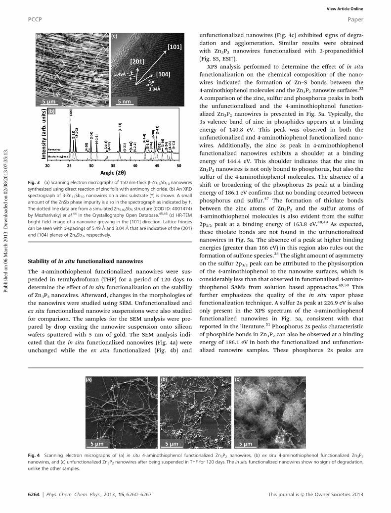
nanowires.The heavier zinc pnictide nanowires were synthesized via a
similar route. The reaction of heated zinc foils with SbCl3
supplied via the vapor phase formed 150 nm-thick Zn4Sb3
nanowires (Fig. 3a). An XRD spectrograph (Fig. 3b) shows theformation of the Zn5.92Sb5 phase of zinc antimonide, nearlyidentical to that previously reported by Mozharivskyj et al.44
The variations in the stoichiometry of Zn4Sb3 have been pre-viously attributed to a zinc void fraction or a zinc substitutionat one of the antimony sites within the crystal lattice.14 Thedotted line displayed is the simulated XRD pattern of thecrystallographic information file (COD ID: 4001474) proposed byMozharivskyj et al.44 in the Crystallography Open Database.45,46
The extra peaks are attributed to the zinc substrate (*) and asmall amount of ZnSb phase impurity (†). No processing wasperformed on the data and the Cu Ka2 doublet peaks stillremain. HR-TEM bright field imaging (Fig. 3c) reveals that thenanowires grow along the [101] axis. Lattice fringes can be seenwith d-spacings of 5.49 Å and 3.04 Å that are characteristic ofthe {201} and {104} planes of Zn4Sb3, respectively. TEM-EDS(Fig. S3b, ESI†) analysis confirmed the Zn4Sb3 stoichiometry ofthe nanowires. The synthesis of both the phosphide andantimonide nanowires via self-catalysis results in the same[101] growth direction. Like the Zn3P2 nanowires, no dropletscan be seen at the tip of the nanowires due to the excess zincbeing vaporized or consumed during reaction shutdown.
Fig. 2 Photograph of a coiled zinc foil (a) before and (b) after the vapor transport of phosphorus. (c) Photograph of Zn3P2 nanowire powder obtained by brushing offthe foils. (d) A transmission electron micrograph from a Zn3P2 nanowire indicating that the growth direction of the nanowires was not altered in the secondexperimental procedure and remained [101]. (e) A scanning electron micrograph of Zn3P2 nanowires obtained by the above-mentioned approach. (f) Photograph ofthe uncoiled zinc foil covered with Zn3P2 nanowires (green deposit) after the vapor transport of phosphorus onto its surface.
Paper PCCP
Publ
ishe
d on
06
Mar
ch 2
013.
Dow
nloa
ded
on 0
2/08
/201
3 07
:35:
13.
View Article Online
6264 Phys. Chem. Chem. Phys., 2013, 15, 6260--6267 This journal is c the Owner Societies 2013
Stability of in situ functionalized nanowires
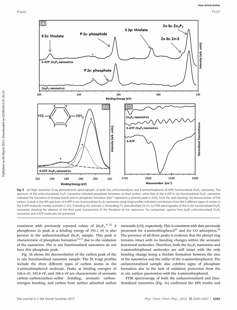
The 4-aminothiophenol functionalized nanowires were sus-pended in tetrahydrofuran (THF) for a period of 120 days todetermine the effect of in situ functionalization on the stabilityof Zn3P2 nanowires. Afterward, changes in the morphologies ofthe nanowires were studied using SEM. Unfunctionalized andex situ functionalized nanowire suspensions were also studiedfor comparison. The samples for the SEM analysis were pre-pared by drop casting the nanowire suspension onto siliconwafers sputtered with 5 nm of gold. The SEM analysis indi-cated that the in situ functionalized nanowires (Fig. 4a) wereunchanged while the ex situ functionalized (Fig. 4b) and
unfunctionalized nanowires (Fig. 4c) exhibited signs of degra-dation and agglomeration. Similar results were obtainedwith Zn3P2 nanowires functionalized with 3-propanedithiol(Fig. S5, ESI†).
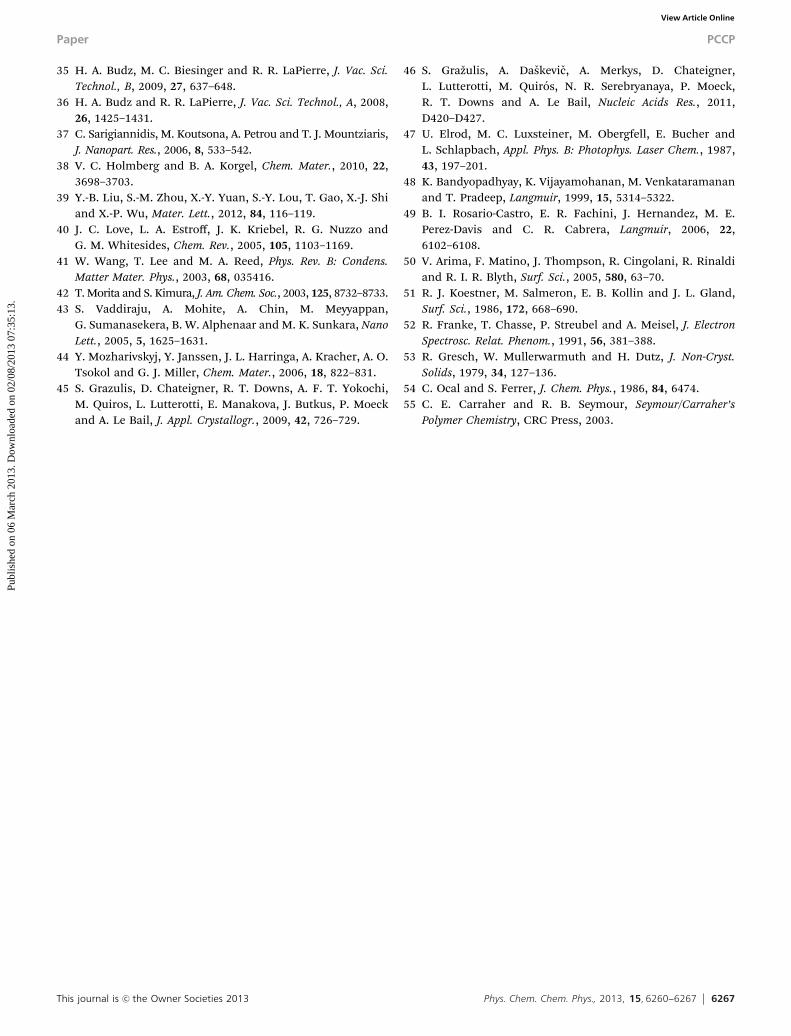
XPS analysis performed to determine the effect of in situfunctionalization on the chemical composition of the nano-wires indicated the formation of Zn–S bonds between the4-aminothiophenol molecules and the Zn3P2 nanowire surfaces.32
A comparison of the zinc, sulfur and phosphorus peaks in boththe unfunctionalized and the 4-aminothiophenol function-alized Zn3P2 nanowires is presented in Fig. 5a. Typically, the3s valence band of zinc in phosphides appears at a bindingenergy of 140.8 eV. This peak was observed in both theunfunctionalized and 4-aminothiophenol functionalized nano-wires. Additionally, the zinc 3s peak in 4-aminothiophenolfunctionalized nanowires exhibits a shoulder at a bindingenergy of 144.4 eV. This shoulder indicates that the zinc inZn3P2 nanowires is not only bound to phosphorus, but also thesulfur of the 4-aminothiophenol molecules. The absence of ashift or broadening of the phosphorus 2s peak at a bindingenergy of 186.1 eV confirms that no bonding occurred betweenphosphorus and sulfur.47 The formation of thiolate bondsbetween the zinc atoms of Zn3P2 and the sulfur atoms of4-aminothiophenol molecules is also evident from the sulfur2p3/2 peak at a binding energy of 163.8 eV.48,49 As expected,these thiolate bonds are not found in the unfunctionalizednanowires in Fig. 5a. The absence of a peak at higher bindingenergies (greater than 166 eV) in this region also rules out theformation of sulfone species.38 The slight amount of asymmetryon the sulfur 2p3/2 peak can be attributed to the physisorptionof the 4-aminothiophenol to the nanowire surfaces, which isconsiderably less than that observed in functionalized 4-amino-thiophenol SAMs from solution based approaches.49,50 Thisfurther emphasizes the quality of the in situ vapor phasefunctionalization technique. A sulfur 2s peak at 226.9 eV is alsoonly present in the XPS spectrum of the 4-aminothiophenolfunctionalized nanowires in Fig. 5a, consistent with thatreported in the literature.51 Phosphorus 2s peaks characteristicof phosphide bonds in Zn3P2 can also be observed at a bindingenergy of 186.1 eV in both the functionalized and unfunction-alized nanowire samples. These phosphorus 2s peaks are
Fig. 3 (a) Scanning electron micrographs of 150 nm-thick b-Zn13Sb10 nanowiressynthesized using direct reaction of zinc foils with antimony chloride. (b) An XRDspectrograph of b-Zn13Sb10 nanowires on a zinc substrate (*) is shown. A smallamount of the ZnSb phase impurity is also in the spectrograph as indicated by †.The dotted line data are from a simulated Zn5.92Sb5 structure (COD ID: 4001474)by Mozharivskyj et al.44 in the Crystallography Open Database.45,46 (c) HR-TEMbright field image of a nanowire growing in the [101] direction. Lattice fringescan be seen with d-spacings of 5.49 Å and 3.04 Å that are indicative of the {201}and {104} planes of Zn4Sb3, respectively.
Fig. 4 Scanning electron micrographs of (a) in situ 4-aminothiophenol functionalized Zn3P2 nanowires, (b) ex situ 4-aminothiophenol functionalized Zn3P2
nanowires, and (c) unfunctionalized Zn3P2 nanowires after being suspended in THF for 120 days. The in situ functionalized nanowires show no signs of degradation,unlike the other samples.
PCCP Paper
Publ
ishe
d on
06
Mar
ch 2
013.
Dow
nloa
ded
on 0
2/08
/201
3 07
:35:
13.
View Article Online
This journal is c the Owner Societies 2013 Phys. Chem. Chem. Phys., 2013, 15, 6260--6267 6265
consistent with previously reported values of Zn3P2.47,52 A
phosphorus 2s peak at a binding energy of 191.1 eV is alsopresent in the unfunctionalized Zn3P2 sample. This peak ischaracteristic of phosphate formation52,53 due to the oxidationof the nanowires. The in situ functionalized nanowires do nothave this phosphate peak.
Fig. 5b shows the deconvolution of the carbon peak of thein situ functionalized nanowire sample. The fit Voigt profilesinclude the three different types of carbon atoms in the4-aminothiophenol molecule. Peaks at binding energies of248.6 eV, 285.6 eV, and 288.6 eV are characteristic of aromaticcarbon–carbon/carbon–sulfur bonding, aromatic carbon–nitrogen bonding, and carbon from surface adsorbed carbon
monoxide (CO), respectively. This is consistent with data previouslypresented for 4-aminothiophenol49 and for CO adsorption.54
The presence of all three peaks is evidence that the phenyl ringremains intact with no bonding changes within the aromaticfunctional molecules. Therefore, both the Zn3P2 nanowires and4-aminothiophenol molecules are still intact with the onlybonding change being a thiolate formation between the zincof the nanowires and the sulfur of the 4-aminothiophenol. Theunfunctionalized sample also exhibits signs of phosphateformation due to the lack of oxidation protection from thein situ surface passivation with the 4-aminothiophenol.
FTIR spectroscopy of both the unfunctionalized and func-tionalized nanowires (Fig. 5c) confirmed the XPS results and
Fig. 5 (a) High resolution X-ray photoelectron spectrographs of both the unfunctionalized and 4-aminothiophenol (4-ATP) functionalized Zn3P2 nanowires. Thespectrum of the unfunctionalized Zn3P2 nanowires indicated phosphate formation on their surface, while that of the 4-ATP in situ functionalized Zn3P2 nanowiresindicated the formation of thiolate bonds and no phosphate formation (the * represents a chlorine peak in ZnCl2 from the acid cleaning). (b) Deconvolution of thecarbon 1s peak in the XPS spectrum of 4-ATP in situ functionalized Zn3P2 nanowires using Voigt profiles indicated contributions from the 3 different types of carbon inthe 4-ATP molecule, namely aromatic C–C/C–S bonding (‡), aromatic C–N bonding (*), and adsorbed CO (†). (c) FTIR spectrographs of the in situ functionalized Zn3P2
nanowires showing the absence of the thiol peak characteristic of the thiolation of the nanowires. For comparison, spectra from both unfunctionalized Zn3P2
nanowires and 4-ATP molecules are presented.
Paper PCCP
Publ
ishe
d on
06
Mar
ch 2
013.
Dow
nloa
ded
on 0
2/08
/201
3 07
:35:
13.
View Article Online

6266 Phys. Chem. Chem. Phys., 2013, 15, 6260--6267 This journal is c the Owner Societies 2013
indicated the formation of thiolate bonds between 4-amino-thiophenol and Zn3P2 nanowires in the functionalized sample.An FTIR spectrograph showing the absence of a peak at2550 cm�1, characteristic of an S–H stretch,55 in the in situfunctionalized nanowires agrees with the XPS result of com-plete deprotonation of the 4-aminothiophenol and bonding ofthe sulfur with zinc (Fig. 5c). For comparison, FTIR spectro-graphs of 4-aminothiophenol, indicating a thiol stretch, andunfunctionalized nanowires with no stretch peak are alsoshown in Fig. 5c.
Conclusions
Zinc phosphide and zinc antimonide nanowires were syn-thesized on a gram-quantity scale by using a direct reactionof the elements in a hot-walled CVD reactor. Additionally, thenanowire surfaces were passivated using an in situ vapor phasetechnique to protect them from oxidation when exposed to theatmosphere and prevented their agglomeration when sus-pended as a colloid. Not only is this all-dry technique simpleto execute, but it is also prevents a native oxide layer fromforming on the nanowires upon exposure to the atmosphere.The absence of this native oxide layer removes the need forchemical etching that could adversely affect the size, morpho-logy, and composition of the nanowires before they are used indevice fabrication. These strategies for the large-scale produc-tion and in situ functionalization of nanowire powders openmany opportunities for not only zinc pnictides, but a broaderrange of nanomaterials to be used in energy conversion devices,despite their surface reactivity and stability short-comings.
Acknowledgements
The authors thank Dr. Jacek Jasinski of the Conn Center forRenewable Energy at the University of Louisville for the TEManalysis of the nanowires. Financial support from the NSF/DOEThermoelectric Partnership Program (CBET# 1048702) is alsogratefully acknowledged.
References
1 T. Zdanowicz, T. Rodziewicz and M. Zabkowska-Waclawek,Sol. Energy Mater. Sol. Cells, 2005, 87, 757–769.
2 W. Shockley and H. J. Queisser, J. Appl. Phys., 1961, 32, 510–519.3 S. R. Taylor, Geochim. Cosmochim. Acta, 1964, 28, 1273–1285.4 C. H. Hsu, B. C. Han, M. Y. Liu, C. Y. Yeh and J. E. Casida,
Free Radicals Biol. Med., 2000, 28, 636–642.5 G. Chen, S. B. Visbeck, D. C. Law and R. F. Hicks, J. Appl.
Phys., 2002, 91, 9362–9367.6 P. Soukiassian, M. H. Bakshi, H. I. Starnberg,
A. S. Bommannavar and Z. Hurych, Phys. Rev. B: Condens.Matter Mater. Phys., 1988, 37, 6496.
7 M. Y. Bashouti, T. Stelzner, A. Berger, S. Christiansen andH. Haick, J. Phys. Chem. C, 2008, 112, 19168–19172.
8 T. Hanrath and B. A. Korgel, J. Am. Chem. Soc., 2004, 126,15466–15472.
9 M. Bhushan and A. Catalano, Appl. Phys. Lett., 1981, 38, 39–41.10 O. Savadogo, Sol. Energy Mater. Sol. Cells, 1998, 52, 361–388.11 J. B. Baxter and E. S. Aydil, Appl. Phys. Lett., 2005, 86, 053114.12 M. Law, L. E. Greene, J. C. Johnson, R. Saykally and
P. D. Yang, Nat. Mater., 2005, 4, 455–459.13 V. Protasenko, D. Bacinello and M. Kuno, J. Phys. Chem. B,
2006, 110, 25322–25331.14 G. J. Snyder, M. Christensen, E. Nishibori, T. Caillat and
B. B. Iversen, Nat. Mater., 2004, 3, 458–463.15 E. S. Toberer, K. A. Sasaki, C. R. I. Chisholm, S. M. Haile,
W. A. Goddard and G. J. Snyder, Phys. Status Solidi RRL,2007, 1, 253–255.
16 M. S. Dresselhaus, G. Chen, M. Y. Tang, R. G. Yang, H. Lee,D. Z. Wang, Z. F. Ren, J. P. Fleurial and P. Gogna, Adv.Mater., 2007, 19, 1043–1053.
17 L. D. Hicks and M. S. Dresselhaus, Phys. Rev. B: Condens.Matter Mater. Phys., 1993, 47, 16631–16634.
18 S. Ren, N. Zhao, S. C. Crawford, M. Tambe, V. Bulovic andS. Gradecak, Nano Lett., 2010, 11, 408–413.
19 G. Z. Shen, Y. Bando, J. Q. Hu and D. Golberg, Appl. Phys.Lett., 2006, 88.
20 R. S. Yang, Y. L. Chueh, J. R. Morber, R. Snyder, L. J. Chouand Z. L. Wang, Nano Lett., 2007, 7, 269–275.
21 P. C. Wu, T. Sun, Y. Dai, Y. H. Sun, Y. Ye and L. Dai, Cryst.Growth Des., 2011, 11, 1417–1421.
22 T. Sun, P. C. Wu, Z. D. Guo, Y. Dai, H. Meng, X. L. Fang,Z. J. Shi, L. Dai and G. G. Qin, Phys. Lett. A, 2011, 375,2118–2121.
23 P. Wu, Y. Dai, Y. Ye, Y. Yin and L. Dai, J. Mater. Chem., 2011,21, 2563–2567.
24 H.-Y. Tuan and B. A. Korgel, Chem. Mater., 2008, 20,1239–1241.
25 S. K. Bux, M. Rodriguez, M. T. Yeung, C. Yang, A. Makhluf,R. G. Blair, J.-P. Fleurial and R. B. Kaner, Chem. Mater., 2010,22, 2534–2540.
26 V. Kumar, J. H. Kim, C. Pendyala, B. Chernomordik andM. K. Sunkara, J. Phys. Chem. C, 2008, 112, 17750–17754.
27 S. Hong, R. Reifenberger, W. Tian, S. Datta, J. I. Hendersonand C. P. Kubiak, Superlattices Microstruct., 2000, 28,289–303.
28 J. A. Larsson, M. Nolan and J. C. Greer, J. Phys. Chem. B,2002, 106, 5931–5937.
29 Z. Y. Li, S. C. Chang and R. S. Williams, Langmuir, 2003, 19,6744–6749.
30 K. Murty, M. Venkataramanan and T. Pradeep, Langmuir,1998, 14, 5446–5456.
31 K. G. Thomas, S. Barazzouk, B. I. Ipe, S. T. S. Joseph andP. V. Kamat, J. Phys. Chem. B, 2004, 108, 13066–13068.
32 P. W. Sadik, S. J. Pearton, D. P. Norton, E. Lambers andF. Ren, J. Appl. Phys., 2007, 101.
33 J. Singh, J. Im, J. E. Whitten, J. W. Soares and D. M. Steeves,Chem. Phys. Lett., 2010, 497, 196–199.
34 J. Singh, J. Im, J. E. Whitten, J. W. Soares, A. M. Meehan andD. M. Steeves, in Nanophotonic Materials V, ed. Z. Gaburro,S. Cabrini and D. Talapin, Spie-Int Soc Optical Engineering,Bellingham, 2008, vol. 7030, pp. T300–T300.
PCCP Paper
Publ
ishe
d on
06
Mar
ch 2
013.
Dow
nloa
ded
on 0
2/08
/201
3 07
:35:
13.
View Article Online
This journal is c the Owner Societies 2013 Phys. Chem. Chem. Phys., 2013, 15, 6260--6267 6267
35 H. A. Budz, M. C. Biesinger and R. R. LaPierre, J. Vac. Sci.Technol., B, 2009, 27, 637–648.
36 H. A. Budz and R. R. LaPierre, J. Vac. Sci. Technol., A, 2008,26, 1425–1431.
37 C. Sarigiannidis, M. Koutsona, A. Petrou and T. J. Mountziaris,J. Nanopart. Res., 2006, 8, 533–542.
38 V. C. Holmberg and B. A. Korgel, Chem. Mater., 2010, 22,3698–3703.
39 Y.-B. Liu, S.-M. Zhou, X.-Y. Yuan, S.-Y. Lou, T. Gao, X.-J. Shiand X.-P. Wu, Mater. Lett., 2012, 84, 116–119.
40 J. C. Love, L. A. Estroff, J. K. Kriebel, R. G. Nuzzo andG. M. Whitesides, Chem. Rev., 2005, 105, 1103–1169.
41 W. Wang, T. Lee and M. A. Reed, Phys. Rev. B: Condens.Matter Mater. Phys., 2003, 68, 035416.
42 T. Morita and S. Kimura, J. Am. Chem. Soc., 2003, 125, 8732–8733.43 S. Vaddiraju, A. Mohite, A. Chin, M. Meyyappan,
G. Sumanasekera, B. W. Alphenaar and M. K. Sunkara, NanoLett., 2005, 5, 1625–1631.
44 Y. Mozharivskyj, Y. Janssen, J. L. Harringa, A. Kracher, A. O.Tsokol and G. J. Miller, Chem. Mater., 2006, 18, 822–831.
45 S. Grazulis, D. Chateigner, R. T. Downs, A. F. T. Yokochi,M. Quiros, L. Lutterotti, E. Manakova, J. Butkus, P. Moeckand A. Le Bail, J. Appl. Crystallogr., 2009, 42, 726–729.
46 S. Grazulis, A. Daskevic, A. Merkys, D. Chateigner,L. Lutterotti, M. Quiros, N. R. Serebryanaya, P. Moeck,R. T. Downs and A. Le Bail, Nucleic Acids Res., 2011,D420–D427.
47 U. Elrod, M. C. Luxsteiner, M. Obergfell, E. Bucher andL. Schlapbach, Appl. Phys. B: Photophys. Laser Chem., 1987,43, 197–201.
48 K. Bandyopadhyay, K. Vijayamohanan, M. Venkataramananand T. Pradeep, Langmuir, 1999, 15, 5314–5322.
49 B. I. Rosario-Castro, E. R. Fachini, J. Hernandez, M. E.Perez-Davis and C. R. Cabrera, Langmuir, 2006, 22,6102–6108.
50 V. Arima, F. Matino, J. Thompson, R. Cingolani, R. Rinaldiand R. I. R. Blyth, Surf. Sci., 2005, 580, 63–70.
51 R. J. Koestner, M. Salmeron, E. B. Kollin and J. L. Gland,Surf. Sci., 1986, 172, 668–690.
52 R. Franke, T. Chasse, P. Streubel and A. Meisel, J. ElectronSpectrosc. Relat. Phenom., 1991, 56, 381–388.
53 R. Gresch, W. Mullerwarmuth and H. Dutz, J. Non-Cryst.Solids, 1979, 34, 127–136.
54 C. Ocal and S. Ferrer, J. Chem. Phys., 1986, 84, 6474.55 C. E. Carraher and R. B. Seymour, Seymour/Carraher’s
Polymer Chemistry, CRC Press, 2003.
Paper PCCP
Publ
ishe
d on
06
Mar
ch 2
013.
Dow
nloa
ded
on 0
2/08
/201
3 07
:35:
13.
View Article Online