Large electroluminescence excitation cross...
6
Large electroluminescence excitation cross section and strong potential gain of erbium in ErYb silicate Bing Wang, Ruimin Guo, Xingjun Wang, Lei Wang, Bing Yin et al. Citation: J. Appl. Phys. 113, 103108 (2013); doi: 10.1063/1.4795153 View online: http://dx.doi.org/10.1063/1.4795153 View Table of Contents: http://jap.aip.org/resource/1/JAPIAU/v113/i10 Published by the American Institute of Physics. Related Articles Laser direct writing of GaN-based light-emitting diodes—The suitable laser source for mesa definition J. Appl. Phys. 113, 103107 (2013) Anisotropy in amorphous films of cross-shaped molecules with an accompanying effect on carrier mobility: Ellipsometric and sum-frequency vibrational spectroscopic studies Appl. Phys. Lett. 102, 101905 (2013) A novel way to improve the quantum efficiency of silicon light-emitting diode in a standard silicon complementary metal–oxide–semiconductor technology J. Appl. Phys. 113, 103106 (2013) UV-visible detector and LED based n-ZnO/p-Si heterojunction formed by electrodeposition AIP Advances 3, 032125 (2013) Optimum experimental design for extended Gaussian disorder modeled organic semiconductor devices J. Appl. Phys. 113, 094903 (2013) Additional information on J. Appl. Phys. Journal Homepage: http://jap.aip.org/ Journal Information: http://jap.aip.org/about/about_the_journal Top downloads: http://jap.aip.org/features/most_downloaded Information for Authors: http://jap.aip.org/authors
Transcript of Large electroluminescence excitation cross...
Large electroluminescence excitation cross section and strong potentialgain of erbium in ErYb silicateBing Wang, Ruimin Guo, Xingjun Wang, Lei Wang, Bing Yin et al. Citation: J. Appl. Phys. 113, 103108 (2013); doi: 10.1063/1.4795153 View online: http://dx.doi.org/10.1063/1.4795153 View Table of Contents: http://jap.aip.org/resource/1/JAPIAU/v113/i10 Published by the American Institute of Physics. Related ArticlesLaser direct writing of GaN-based light-emitting diodes—The suitable laser source for mesa definition J. Appl. Phys. 113, 103107 (2013) Anisotropy in amorphous films of cross-shaped molecules with an accompanying effect on carrier mobility:Ellipsometric and sum-frequency vibrational spectroscopic studies Appl. Phys. Lett. 102, 101905 (2013) A novel way to improve the quantum efficiency of silicon light-emitting diode in a standard silicon complementarymetal–oxide–semiconductor technology J. Appl. Phys. 113, 103106 (2013) UV-visible detector and LED based n-ZnO/p-Si heterojunction formed by electrodeposition AIP Advances 3, 032125 (2013) Optimum experimental design for extended Gaussian disorder modeled organic semiconductor devices J. Appl. Phys. 113, 094903 (2013) Additional information on J. Appl. Phys.Journal Homepage: http://jap.aip.org/ Journal Information: http://jap.aip.org/about/about_the_journal Top downloads: http://jap.aip.org/features/most_downloaded Information for Authors: http://jap.aip.org/authors

Large electroluminescence excitation cross section and strong potentialgain of erbium in ErYb silicate
Bing Wang,1,a) Ruimin Guo,1,2 Xingjun Wang,1,b) Lei Wang,1 Bing Yin,1 and Zhiping Zhou1,b)
1State Key Laboratory of Advanced Optical Communication Systems and Networks, School of ElectronicsEngineering and Computer Science, Peking University, Beijing 100871, China2Division of Biological, Energy and Environmental Measurement, National Institute of Metrology,Beijing 100013, China
(Received 12 September 2012; accepted 26 February 2013; published online 14 March 2013)
1.53 lm electroluminescence of erbium was observed in ErYb silicate metal-insulator-silicon light
emitting device (MISLED). The erbium ions were excited by direct impact of hot carriers at
electric field higher than 7 MV/cm. The conduction and carrier injection mechanisms were
investigated. The impact excitation cross section of Er ions was measured to be 3� 10�14 cm2,
three times of Er-doped SiO2 MISLED. Rate equation modeling suggests that strong potential
material’s gain of more than 23 dB/cm from the ErYb silicate may be achieved by electrical
pumping. VC 2013 American Institute of Physics. [http://dx.doi.org/10.1063/1.4795153]
I. INTRODUCTION
A key challenge that has not been well solved in silicon
photonics is the lack of a fully silicon technology-
compatible electrical-pumped light source, especially a
laser.1 A great amount of methods have been proposed and
developed to pursuit a solution, including silicon nanocrys-
tals, silicon-rich oxides/nitrides and Er-doping,2–4 tensile
strained epitaxial-Ge,5,6 and so on. Field-effect electrolumi-
nescence (EL) operation and possibility of reaching popula-
tion inversion have been demonstrated in silicon
nanocrystals.2,4 Recently, the first report of electrical-
pumped lasing in Ge-on-Si makes this approach very promis-
ing.6 Er-doping has been long thought to be perspective for
silicon light source and amplifier due to its luminescence at
the standard telecommunication wavelength of 1.55 lm. The
method of embedding Er-doped light emitting materials into
silicon slot waveguide can fulfill the requirements of
electrical-pumping and silicon technology compatible simul-
taneously.7 However, the relatively small gain supplied by
Er-doped SiO2 requires a high-Q cavity (Q� 105) to gener-
ate lasing.8 To sustain high Q values in slot waveguide based
cavities, the propagation loss of slot waveguide need to be
reduced, at least lower than the material gain, while this still
remains to be a challenge.
A substitute method for the Er-doped slot waveguide
used for electrical pumping is to use a high gain material,
which can loosen the requirement of high Q cavity. The Er
silicate represents such a candidate. In recent years, Er sili-
cate compounds have attracted intense investigations due to
their efficient luminescence at 1.53 lm and technical com-
patibility with silicon.9,10 As compounds, Er concentrations
in silicates can reach to stoichiometric values and can be eas-
ily changed by co-doping other similar rare earth elements
such as yttrium (Y) and ytterbium (Yb),11–13 which is
necessary to reduce the neighboring Er ions induced concen-
tration quenching and up-conversion effects. In addition, Yb
can be used as sensitizer for Er.14 Recently, we have investi-
gated the ErYb silicate as light emitting and optical gain
materials on silicon platform. Strong light emission and opti-
cal signal enhancement have been observed in ErYb silicate
thin films and waveguides.15–19 The sensitization effect of
Yb for Er in silicate has been also studied.15 Furthermore,
although the ErYb silicate is insulating, we demonstrated
that by injecting carriers into silicate films through Fowler-
Nordheim (FN) tunneling, 1.53 lm Er EL can be achieved.20
This is very promising since the inclusion of ErYb silicate
into electrical-pumped slot waveguide may have more
advantages than using Er-doped SiO2 considering that the
silicate may supply higher gain. However, the important EL
property of excitation cross section of Er ion in the silicate
has not been investigated yet. Furthermore, using available
material’s parameters a suitable modeling to predict the pop-
ulation inversion and gain properties of the silicate under
electrical pumping is essential for the future design and fab-
rication of devices.
In this work, we investigated the 1.53 lm EL and excita-
tion cross section of ErYb silicate in metal-insulator-silicon
light emitting device (MISLED). Our experimental results
demonstrate good excitation property of the ErYb silicate
and modeling analysis indicates that strong potential materi-
al’s gain may be achieved when using electrical pumping.
II. EXPERIMENT AND RESULTS
A 60 nm-thick ErYb silicate thin film was deposited on
a 40 p-type c-Si wafer by magnetron-sputtering using a mixed
compound target. Rutherford backscattering and X-ray fluo-
rescence spectroscopy indicates that the film’s composition
is close to the stoichiometric value of RE2SiO5. The Er con-
centration is about 1.9� 1021 cm�3 and the Er/Yb ratio is
about 1:9.20 The as-deposited ErYb silicate film was then
annealed in furnace at 1050 �C in N2 ambient for half an
hour to be crystallized. Detailed description of the film’s
a)This author has moved to Singapore and can be contacted via
[email protected])E-mail addressess: [email protected] and [email protected].
0021-8979/2013/113(10)/103108/5/$30.00 VC 2013 American Institute of Physics113, 103108-1
JOURNAL OF APPLIED PHYSICS 113, 103108 (2013)

deposition and characterization can be found in previous
work.20 Another layer of 60 nm-thick SiON (refractive index
n¼ 1.778) was deposited on top of the ErYb silicate film by
plasma-enhanced chemical vapor deposition (PECVD).
Aluminum was sputtered on the backside of the substrate to
be used as back-electrode. Square shape (0.5 mm� 0.5 mm)
indium-tin oxide (ITO) electrode was deposited and pat-
terned by photolithography as the top-electrode. A schematic
cross-sectional view is shown in Figure 1(a).
A Keithley 2611 SourceMeter was used to characterize
the current-voltage (I-V) property of the device. Square
shape current pulse was applied on the device to excite the
Er ions. EL spectra were collected by a monochromator
attached with an InGaAs photodetector (PD) and amplified
by a lock-in amplifier (LIA) synchronized to the current
pulse. Time-resolved EL signals were measured at 1.53 lm
and recorded by an oscilloscope connected to the PD. During
the EL operation, ITO electrodes were biased as cathodes.
Figure 1(b) shows the I-V curve of the device. To reveal
the conduction mechanism, the inset shows the FN plot of
the I-V curve. According to the FN tunneling formula,
J/E2¼Aexp(�B/E), where J is current density, E is electric
filed, A and B are constants, the relation between J/E and 1/Eshould be displayed by a linear line in FN plot. Obviously, in
the inset the I-V curve follows the FN tunneling very well.
The tunneling current started from about 6 MV/cm. The
strong E field can accelerate the tunneled carriers to gain
enough kinetic energy to impact and excite Er ions (for the
1.53 lm EL emission, the lowest energy to excite Er ion is
about 0.8 eV). As a comparison, Figure 1(c) shows the I-V
curve and FN plot of reference samples which have only ei-
ther SiON or ErYb silicate as insulating layer (thick-
ness¼ 60 nm) in MIS structure. The SiON sample follows
the FN tunneling very well. No breakdown of the SiON film
happened when electric field became over 8 MV/cm. The
ErYb silicate sample cannot conduct stably when the applied
electric field exceeds about 6 MV/cm (38� 40 V). At this
point the current conducted through the ErYb silicate film
showed a sudden increase and the film became destructive
breakdown. Even though, in the inset it seems before the
breakdown of the silicate film it follows FN tunneling in the
range of 1.6� 10�7 cm/V< 1/E< 2� 10�7 cm/V, as demon-
strated by the green guideline. The breakdown threshold
voltage of the ErYb silicate is lower than the SiON. When
stacked together in the EL device, even when the applied
voltage exceeds the breakdown threshold of the silicate, it is
lower than the SiON. The current conducted through the de-
vice is clamped by the SiON and no sudden increase of cur-
rent can happen. Therefore, the EL device can sustain a high
electric field and work stably in the principle of FN tunnel-
ing. The carriers (electrons and holes) from the ITO and Si
substrate can tunnel through the energy barrier and be
injected into the insulating layers and accelerated by the
strong electric field to gain kinetic energy to impact excite
Er ions. The barriers’ heights of the silicate/SiON and sili-
cate/Si are unknown yet. Once available they will be helpful
for future engineering of the device. The function of the
SiON layer is similar to the SiNx layer used for current limit-
ing in our previous work.20 Here, the SiNx layer is replaced
by the SiON layer which is expected to have a higher con-
ductivity than SiNx,21 and therefore it can improve the cur-
rent injection ability of the device in addition to the enabling
of the carrier tunneling. The smooth I-V curve can be well
repeated and the device worked stably under electrical bias.
Figure 2(a) shows the EL spectra of the device, meas-
ured using current pulse with different amplitude from
1.5 lA to 5lA. The EL spectra profiles are identical to the
1.53 lm PL spectra (PL not shown). This indicates that the
EL is due to the radiative transition of Er ion from 4I13/2 to4I15/2 level. The EL spectra are peaked at 1531 nm and the
spectra structure is due to the Stark splitting of the referred
FIG. 1. (a) Cross sectional view of the ErYb silicate MISLED; (b) current-
voltage (I-V) curve of the device under forward bias; the inset shows the
F-N plot of the I-V curve. (c) I-V curves and FN plots of SiON (black color)
and ErYb silicate (red color) MIS structure. In the inset, the green and blue
lines are guides for the eye.
103108-2 Wang et al. J. Appl. Phys. 113, 103108 (2013)
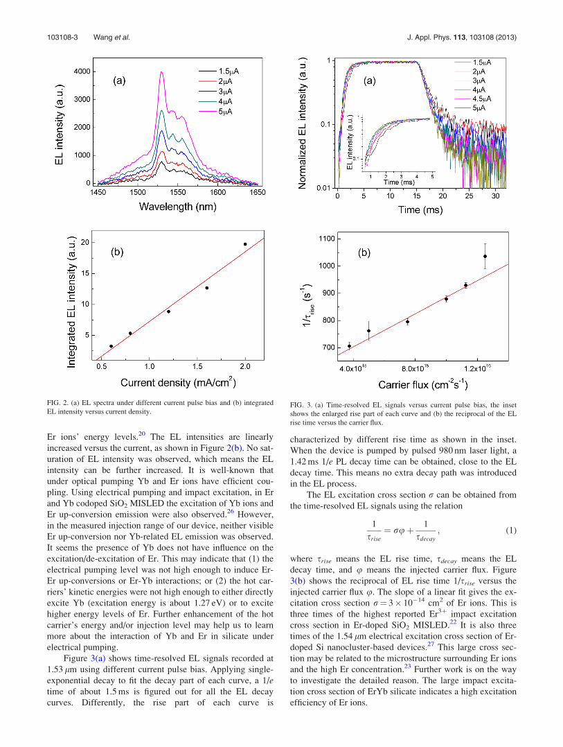
Er ions’ energy levels.20 The EL intensities are linearly
increased versus the current, as shown in Figure 2(b). No sat-
uration of EL intensity was observed, which means the EL
intensity can be further increased. It is well-known that
under optical pumping Yb and Er ions have efficient cou-
pling. Using electrical pumping and impact excitation, in Er
and Yb codoped SiO2 MISLED the excitation of Yb ions and
Er up-conversion emission were also observed.26 However,
in the measured injection range of our device, neither visible
Er up-conversion nor Yb-related EL emission was observed.
It seems the presence of Yb does not have influence on the
excitation/de-excitation of Er. This may indicate that (1) the
electrical pumping level was not high enough to induce Er-
Er up-conversions or Er-Yb interactions; or (2) the hot car-
riers’ kinetic energies were not high enough to either directly
excite Yb (excitation energy is about 1.27 eV) or to excite
higher energy levels of Er. Further enhancement of the hot
carrier’s energy and/or injection level may help us to learn
more about the interaction of Yb and Er in silicate under
electrical pumping.
Figure 3(a) shows time-resolved EL signals recorded at
1.53 lm using different current pulse bias. Applying single-
exponential decay to fit the decay part of each curve, a 1/etime of about 1.5 ms is figured out for all the EL decay
curves. Differently, the rise part of each curve is
characterized by different rise time as shown in the inset.
When the device is pumped by pulsed 980 nm laser light, a
1.42 ms 1/e PL decay time can be obtained, close to the EL
decay time. This means no extra decay path was introduced
in the EL process.
The EL excitation cross section r can be obtained from
the time-resolved EL signals using the relation
1
srise¼ ruþ 1
sdecay; (1)
where srise means the EL rise time, sdecay means the EL
decay time, and u means the injected carrier flux. Figure
3(b) shows the reciprocal of EL rise time 1/srise versus the
injected carrier flux u. The slope of a linear fit gives the ex-
citation cross section r¼ 3� 10�14 cm2 of Er ions. This is
three times of the highest reported Er3þ impact excitation
cross section in Er-doped SiO2 MISLED.22 It is also three
times of the 1.54 lm electrical excitation cross section of Er-
doped Si nanocluster-based devices.27 This large cross sec-
tion may be related to the microstructure surrounding Er ions
and the high Er concentration.23 Further work is on the way
to investigate the detailed reason. The large impact excita-
tion cross section of ErYb silicate indicates a high excitation
efficiency of Er ions.
FIG. 2. (a) EL spectra under different current pulse bias and (b) integrated
EL intensity versus current density.FIG. 3. (a) Time-resolved EL signals versus current pulse bias, the inset
shows the enlarged rise part of each curve and (b) the reciprocal of the EL
rise time versus the carrier flux.
103108-3 Wang et al. J. Appl. Phys. 113, 103108 (2013)
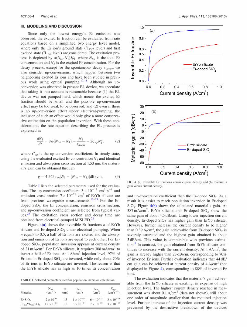
III. MODELING AND DISCUSSION
Since only the lowest energy’s Er emission was
observed, the excited Er fraction can be evaluated from rate
equations based on a simplified two energy level model,
where only the Er ion’s ground state (4I15/2 level) and first
excited state (4I13/2 level) are considered. The excitation pro-
cess is depicted by r(Ntot-N1)J/q, where Ntot is the total Er
concentration and N1 is the excited Er concentration. For the
decay process, except for the spontaneous decay sdecay, we
also consider up-conversions, which happen between two
neighboring excited Er ions and have been studied in previ-
ous work using optical pumping.17,18 Although no up-
conversion was observed in present EL device, we speculate
that taking it into account is reasonable because (1) the EL
device was not pumped hard, which means the excited Er
fraction should be small and the possible up-conversion
effect may be too weak to be observed; and (2) even if there
is no up-conversion effect under electrical-pumping, the
inclusion of such an effect would only give a more conserva-
tive estimation on the population inversion. With these con-
siderations, the rate equation describing the EL process is
expressed as
dN1
dt¼ ruðNtot � N1Þ �
N1
sdecay� 2CupN2
1 ; (2)
where Cup is the up-conversion coefficient. In steady state,
using the evaluated excited Er concentration N1 and identical
emission and absorption cross section at 1.53 lm, the materi-
al’s gain can be obtained through
g ¼ 4:343rem½N1 � ðNtot � N1Þ�dB=cm: (3)
Table I lists the selected parameters used for the evalua-
tion. The up-conversion coefficient 3� 10�17 cm3 s�1 and
emission cross section 7� 10�21 cm2 of ErYb silicate are
from previous waveguide measurements.17–19 For the Er-
doped SiO2, the Er concentration, emission cross section,
and up-conversion coefficient are selected from typical val-
ues.24 The excitation cross section and decay time are
obtained from electrical-pumped MISLED.22
Figure 4(a) shows the invertible Er fractions n of ErYb
silicate and Er-doped SiO2 under electrical pumping. When
n equals to 0.5, a half of Er ions are excited and the absorp-
tion and emission of Er ions are equal to each other. For Er-
doped SiO2, population inversion appears at current density
of 21 mA/cm2. For ErYb silicate, it requires 308 mA/cm2 to
invert a half of Er ions. At 1 A/cm2 injection level, 97% of
Er ions in Er-doped SiO2 are inverted, while only about 70%
of Er ions in ErYb silicate are inverted. The reason is that
the ErYb silicate has as high as 10 times Er concentration
and up-conversion coefficient than the Er-doped SiO2. As a
result it is easier to reach population inversion in Er-doped
SiO2. Figure 4(b) shows the calculated material’s gain. At
387 mA/cm2, ErYb silicate and Er-doped SiO2 show the
same gain of about 4.5 dB/cm. Using lower injection current
density, Er-doped SiO2 has higher gain than ErYb silicate.
However, further increase the current density to be higher
than 0.39 A/cm2, the gain achievable from Er-doped SiO2 is
severely saturated and the highest gain obtained is about
5 dB/cm. This value is comparable with previous estima-
tion.8 In contrast, the gain obtained from ErYb silicate con-
tinues to increase with the current density. At 1 A/cm2, the
gain is already higher than 23 dB/cm, corresponding to 70%
of inverted Er ions. Further evaluation indicates that 44 dB/
cm gain can be achieved at current density of 4 A/cm2 (not
displayed in Figure 4), corresponding to 88% of inverted Er
ions.
The evaluation indicates that the material’s gain achiev-
able from the ErYb silicate is exciting, in expense of high
injection level. The highest current density reached in mea-
surement was about 0.1 A/cm2 (data not shown), still about
one order of magnitude smaller than the required injection
level. Further increase of the injection current density was
prevented by the destructive breakdown of the devices
TABLE I. Selected parameters used for population inversion calculation.
Material
Ntot
(cm�3)
s2
(ms)
rex
(cm2)
rem
(cm2)
Cup
(cm3s�1)
Er-SiO2 2� 1020 1.5 1� 10�14 6� 10�21 3� 10�18
Er0.2Yb1.8SiO5 1.9� 1021 1.5 3� 10�14 7� 10�21 3� 10�17
FIG. 4. (a) Invertible Er fractions versus current density and (b) material’s
gain versus current density.
103108-4 Wang et al. J. Appl. Phys. 113, 103108 (2013)

mainly due to the silicate thin film’s quality. Previously, in
Tb-doped SiO2 MISLED a high injection level of 4 A/cm2
was achieved.25 Improvements are on the way to improve
the material quality, to increase the breakdown electric field
strength and the injection level of ErYb silicate. In addition,
it should be noted that in our evaluation the current density
for population inversion may be overestimated due to the
included up-conversion effect. Therefore, the current density
may not need to be as high as we estimated. Recently, we
observed a 1.7 dB optical signal enhancement at 1.53 lm in
ErYb silicate embedded silicon slot waveguide using
1480 nm optical pumping.19 The propagation loss was about
15 dB/cm and the waveguide structure is suitable for current
injection. Considering the evaluated highest achievable ma-
terial gain of 44 dB/cm under electrical-pumping and a con-
finement factor C of 0.3 in the slot region, about 13 dB/cm
mode gain can be supplied. This is already close to the prop-
agation loss of 15 dB/cm we measured. We estimate that the
loss was due to the scattering in the polycrystalline upper sil-
icon, in ErYb silicate, and the roughness of the surface and
sidewall of the silicon stripe. Further optimization of the
design, processing, and fabrication should be able to reduce
the waveguide loss and net gain may be achieved in ErYb
silicate embedded slot waveguide using electrical-pumping.
IV. CONCLUSIONS
EL spectra and excitation cross section of Er were inves-
tigated in ErYb silicate MISLED. The 1.53 lm EL was
induced by hot carriers’ impact excitation of Er ions. A large
impact excitation cross section of 3� 10�14 cm2 was
obtained. Modeling and evaluation indicate that about 70%
population inversion and 23 dB/cm material’s gain are
achievable from the ErYb silicate at an injection level of
1 A/cm2. The ErYb silicate is a potential candidate for
electrical-pumped light source for silicon photonics.
ACKNOWLEDGMENTS
This work was supported by Peking University’s 985
startup fund and National Natural Science Foundation of
China under Grant Nos. 61036011 and 60907024.
1L. C. Kimerling, L. Dal Negro, S. Saini, Y. Yi, D. Ahn, S. Akiyama,
D. Cannon, J. Liu, J. G. Sandland, D. Sparacin, J. Michel, K. Wada, and
M. R. Watts, in Silicon Photonics: Topics in Applied Physics, edited by L.
Pavesi and D. J. Lockwood (Springer. New York, 2004).2R. J. Walters, G. I. Bourianoff, and H. A. Atwater, Nature Mater. 4, 143,
(2005).3S. Yerci, R. Li, and L. Dal Negro, Appl. Phys. Lett. 97, 081109 (2010)4O. Jambois, F. Gourbilleau, A. J. Kenyon, J. Montserrat, R. Rizk, and B.
Garrido, Opt. Express 18, 2230 (2010).5J. F. Liu, X. C. Sun, R. Camacho-Aguilera, L. C. Kimerling, and
J. Michel, Opt. Lett. 35, 679 (2010).6R. E. Camacho-Aguilera, Y. Cai, N. Patel, J. T. Bessette, M. Romagnoli,
L. C. Kimerling, and J. Michel, Opt. Express 20, 11316, (2012).7C. Angulo Barrios and M. Lipson, Opt. Express 13, 10092 (2005).8K. Preston and M. Lipson, Opt. Express 17, 1527 (2009).9H. Isshiki, M. J. A. de Dood, A. Polman, and T. Kimura, Appl. Phys. Lett.
85, 4343 (2004).10M. Miritello, R. L. Savio, F. Iacona, G. Franzo, A. Irrera, A. M. Piro,
C. Bongiorno, and F. Priolo, Adv. Mater. 19, 1582 (2007).11K. Suh, M. Lee, J. S. Chang, H. Lee, N. Park, G. Y. Sung, and J. H. Shin,
Opt. Express 18, 7724 (2010).12X. J. Wang, G. Yuan, H. Isshiki, T. Mimura, and Z. Zhou, J. Appl. Phys.
108, 013506 (2010).13M. Miritello, P. Cardile, R. L. Savio, and F. Priolo, Opt. Express 19,
20761 (2011).14C. Strohhofer and A. Polman, J. Appl. Phys. 90, 4314 (2001).15M. Vanhoutte, B. Wang, Z. Zhou, J. Michel, and L. C. Kimerling, in
Group IV Photonics (IEEE, 2010), pp. 308–310.16X. J. Wang, B. Wang, L. Wang, R. M. Guo, H. Isshiki, T. Kimura, and
Z. Zhou, Appl. Phys. Lett. 98, 071903 (2011).17R. M. Guo, X. J. Wang, K. Zang, B. Wang, L. Wang, L. F. Gao, and Z.
Zhou, Appl. Phys. Lett. 99, 161115 (2011).18L. Wang, R. M. Guo, B. Wang, X. J. Wang, and Z. Zhou, IEEE Photon.
Technol. Lett. 24, 900 (2012).19R. M. Guo, B. Wang, X. J. Wang, L. Wang, L. J. Jiang, and Z. Zhou, Opt.
Lett. 37, 1427 (2012).20B. Wang, R. M. Guo, X. J. Wang, L. Wang, L. Y. Hong, B. Yin, L. F.
Gao, and Z. Zhou, Opt. Mater. 34, 1371 (2012).21X. Guo and T.-P. Ma, IEEE Electron Device Lett. 19, 207 (1998).22M. E. Castagna, S. Coffa, M. Monaco, A. Muscara, L. Caristia, S. Lorenti,
A. Messina, Mater. Sci. Eng., B 105, 83 (2003).23J. M. Sun, S. Prucnal, W. Skorupa, T. Dekorsy, A. Muchlich, M. Helm,
L. Rebohle, and T. Gebel, J. Appl. Phys. 99, 103102 (2006).24E. Snokes, G. N. van den Hoven, and A. Polman, IEEE J. Quantum
Electron. 32, 1680 (1996).25J. M. Sun, L. Rebohle, S. Prucnal, M. Helm, and W. Skorupa, Appl. Phys.
Lett. 92, 071103 (2008).26S. Prucnal, L. Rebohle, and W. Skorupa, J. Non-Cryst. Solids 357, 915,
(2011).27F. Iacona, D. Pacifici, A. Irrera, M. Miritello, G. Franzo, F. Priolo, D.
Sanfilippo, G. Di Stefano, and P. G. Fallica, Appl. Phys. Lett. 81, 3242,
(2002).
103108-5 Wang et al. J. Appl. Phys. 113, 103108 (2013)