Lanthanide Ions Doping Effects on Structural, …...III Applications of ferroelectric thin films 27...
166
Lanthanide Ions Doping Effects on Structural, Electrophysical and Functional Properties of Sol-gel Fabricated PbTiO 3 Thin Films Dissertation Zur Erlangung des akademischen Grades Doktor der Ingenieurwissenschaften (Dr.-Ing.) der Technischen Fakultät der Christian-Albrechts-Universität zu Kiel Sergey Yakovlev Kiel 2004
Transcript of Lanthanide Ions Doping Effects on Structural, …...III Applications of ferroelectric thin films 27...

Lanthanide Ions Doping Effects on Structural, Electrophysical and Functional Properties of
Sol-gel Fabricated PbTiO3 Thin Films
Dissertation
Zur Erlangung des akademischen Grades
Doktor der Ingenieurwissenschaften
(Dr.-Ing.)
der Technischen Fakultät
der Christian-Albrechts-Universität zu Kiel
Sergey Yakovlev
Kiel 2004

2
Supervisor: Prof. Dr. F. Faupel
Co-supervisor: Prof. Dr. M. Es-Souni

3
Contents
Acknowledgements 5 Abstract 7 Introduction 9 I Basics of Ferroelectric Materials 12 I.1. What is ferroelectricity? 12 I.2. Phase transitions in ferroelectric materials 18 I.3. Properties of some well known ferroelectric materials 20 II Methods for ferroelectric thin films processing 22 II.1. Electron beam evaporation 22 II.2. Pulsed laser deposition (PLD) 22 II.3. Multi-ion-beam reactive sputter deposition (MIBRSD) 23 II.4. Organometallic chemical vapour deposition (OMCVD) 23 II.5. Sol-gel processing of thin films 24 III Applications of ferroelectric thin films 27 III.1. Non-volatile and Dynamic Random Access Memories 27 III.2. Microelectromechanical systems 28 III.3. IR detectors 30 IV Characterization of ferroelectric materials 35 IV.1. X-ray diffractometry 35 IV.2. Raman spectroscopy 37 IV.3. X-ray photoelectron spectroscopy 38 IV.4. Scanning electron microscopy 39 IV.5 Atomic force microscopy 40 IV.6. Ellipsometry 41 IV.7. Ferroelectric hysteresis characterization 44 IV.8. Dielectric properties measurements 45 IV.9. Leakage current measurements 46 IV.10. Determination of pyroelectric coefficient of ferroelectric materials 47 IV.11. Measurements of piezoelectric characteristics of ferroelectric
materials 48
V Overview of the properties of lead-based perovskite-type ferroelectric thin films: microstructural and compositional aspects
51
V.1. Optical properties 51 V.2. Microstructure and crystallization kinetics 53 V.3. Raman scattering 55 V.4. Dielectric properties 57 V.5. Ferroelectric properties 61 V.6. Curie phase transition temperature 64 V.7. Doping effects 66 V.8. Leakage currents 69 V.9. Pyroelectric and piezoelectric properties of ferroelectric thin films 73

4
VI Aims of this work 75 VII Preparation and characterization of lanthanide ions doped
PbTiO3 thin films: experimental details 77
VII.1. Sol-gel fabrication of pure and rare-earth substituted PbTiO3 thin films and optimisation of deposition parameters
77
VII.2. Experimental details on structural and electrophysical properties characterization
84
VIII Experimental results 90 VIII.1. Structural properties of rare-earth substituted PbTiO3 thin films 90 VIII.2. Raman scattering from pure and rare-earth substituted PbTiO3 thin
films 99
VIII.3. Refractive indices and extinction coefficients of lanthanide ions doped lead titanate thin films
100
VIII.4. Room temperature dielectric properties of pure and doped lead titanate thin films
103
VIII.5. Effect of lanthanide ions doping on the ferroelectric-paraelectric phase transition temperature
104
VIII.6. Ferroelectric properties of PbTiO3 thin films doped with lanthanide ions
107
VIII.7. Thickness effects and contribution of interfacial bottom electrode-thin film layer into small signal dielectric properties of doped lead titanate thin films
108
VIII.8. Field-dependent dielectric properties of pure and doped lead titanate thin films
109
VIII.9. Voltage-, temperature- and thickness-dependent leakage currents in pure and doped lead titanate thin films
111
IX Discussions 116 IX.1. Structural properties, phase content and preferred orientation of
PbTiO3 thin films doped with the elements of lanthanide series 116
IX.2. Raman scattering from pure and lanthanide ions doped PbTiO3 thin films
121
IX.3. Refractive indices and extinction coefficients of lanthanide ions doped lead titanate thin films
122
IX.4. Room temperature dielectric properties of pure and doped lead titanate thin films
124
IX.5. Effect of lanthanide ions doping on the ferroelectric-paraelectric phase transition temperature
125
IX.6. Ferroelectric properties of PbTiO3 thin films doped with the elements of lanthanide series
127
IX.7. Thickness- and field-dependent dielectric properties of pure and doped lead titanate thin films
128
IX.8. Voltage-, temperature- and thickness-dependent leakage currents in pure and doped lead titanate thin films
131
X Choice of application: doped PbTiO3 thin films for pyroelectric and piezoelectric detectors
137
XI Summary and conclusions 144 List of references 147 Appendix 156 Curriculum Vitae 164

5
Acknowledgements
I express my deep gratitude to many people who contributed through their support,
experience and friendship to this work. In particular I am in debt to
Prof. Dr. M. Es-Souni for supervision and giving me the opportunity to work at the
University of Applied Sciences of Kiel, Institute for Materials and Surface Technology
(IMST), his support, confidence and providing facilities for this work to be accomplished.
Prof. Dr. F. Faupel (Department of Engineering, Christian-Albrechts University, Kiel)
for the warm encouragement and being co-supervisor during preparation of the thesis.
C.-H. Solterbeck (University of Applied Sciences, Institute for Materials and Surface
Technology (IMST), Kiel) for the helpful discussions and the assistance in AFM, dielectric
and ferroelectric measurements.
Dr. M. Kuhnke (University of Applied Sciences, Institute for Materials and Surface
Technology (IMST), Kiel) for the assistance in pyroelectric and piezoelectric
characterizations.
Dr. V. Zaporojtchenko and J. Žekonytė (Department of Engineering, Christian-
Albrechts University, Kiel) for the help during XPS experiments.
Dr. K. Rätzke and T. Metzing (Department of Engineering, Christian-Albrechts
University, Kiel) for the assistance and troubleshooting during XRD measurements.
Dr. M. Avdeev (Materials Science Division, Argonne National Laboratory) for useful
discussions, and different kinds of support.

6
A. Piorra, E. Girdauskaitė and A. Dreher (University of Applied Sciences, Institute for
Materials and Surface Technology (IMST), Kiel) for their help in specimen preparation and
creating cooperative and pleasant atmosphere in the laboratories.
Prof. Dr. E. Skou, S.W. Lena (Department of Chemistry, University of Southern
Denmark, Odense, Denmark), Prof. Dr. F. Tuczek, U. Cornelissen (Department of
Mathematics and Natural Sciences, Christian-Albrechts University of Kiel, Kiel, Germany)
for their help in Raman measurements.
Prof. Dr. A. Neiman (Department of Inorganic Chemistry, Ural State University,
Ekaterinburg, Russia), Dr. V. Kharton (Department of Ceramics and Glass Engineering,
University of Aveiro, Portugal) and Prof. Dr. I. Smirnov (Department of Materials Science,
Moscow State Institute of Electronics and Mathematics (Technical University), Russia), for
useful discussions and encouragement.
Finally I express the deep gratitude to my family and friends for the support over the
years.

7
Abstract
Ferroelectrics belong to the special class of non-centrosymmetric polar dielectrics in
which spontaneous polarization of lattice can be switched via the application of an external
electric field. In particular, perovskite-type lead titanate-based ferroelectrics became the most
prominent candidates for applications in different kinds of modern transducers, sensors and
actuators. Particular interest in these materials is driven by their unique dielectric,
ferroelectric, pyroelectric and piezoelectric characteristics. The application of these materials
in thin film form is even more attractive since it allows direct integration into existent
semiconductor technology. The properties of lead-titanate based ferroelectrics are known to
strongly depend on the stoichiometry and nature of substituent elements either on Pb (A) or Ti
(B) sites. In this respect appropriate doping by different elements offers the possibility to tune
materials functional properties.
Lanthanides (rare-earths) constitute a series of chemically similar elements with
gradually decreasing ionic radius. Therefore, systematic investigations of lanthanide ions
doped ferroelectrics can reveal the effect of the ionic radius of substituent on the structural
and electrophysical properties of the host material. To our knowledge, these investigations are
still lacking. Moreover, interrelation between doping level and performance of the materials
must be established.
In the present work, a modified sol-gel method was adopted to fabricate lead titanate
thin films doped with Ce, Sm, Dy, Er and Yb. Two different substrate heterostructures
including Si/SiO2/Ti/(111)-textured Pt and Si/SiO2/Ti/(111)-Pt/LNO (polycrystalline
lanthanum nickel oxide LaNiO3 ) were used. The structural properties, phase composition and
preferentially oriented state of the films were analyzed by means of X-ray diffractometry
(XRD), including pole figure and fibre texture (FT) analyses, Raman spectroscopy, scanning
electron microscopy (SEM) and atomic force microscopy (AFM). The optical, dielectric,
ferroelectric and leakage current properties were investigated in order to reveal the effects of
nature and concentration of doping ions, substrate heterostructure and film thickness on the
main characteristics of the films.

8
Fine grained (grain size was found to be in the range of 100-140 nm) homogeneous
microstructures were obtained under the conditions optimised in this work. The formation of
the perovskite phase was confirmed by means of X-ray diffractometry and Raman
spectroscopy. The softening of the E(1TO) soft mode was found for pure and doped films.
Doping with rare-earth ions caused further decrease of the soft phonon frequency indicating
decrease of the ferroelectric order in the films. The results are discussed in terms of combined
effects of stress state, grain size and doping. Additionally, XRD characterization revealed
decrease of the lattice tetragonality for all doping ions investigated.
Pole figure and fibre texture plot analyses of the films deposited on (111) textured Pt
bottom electrode showed the effect of lanthanide ions doping on preferred orientation of the
films. (100) out-of-plane texture was revealed for pure and Dy and Er substituted films. Ce,
Sm and Yb substituted films were found to be characterized by (100)+(111) preferred
orientations with no in-plane alignment.
It is demonstrated that the electrophysical properties of the films can be effectively
tuned via doping by rare-earth ions. An interrelation between the atomic number/ionic radius
of lanthanides and the low and high (optical) frequency dielectric properties is shown and
discussed in terms of polarizability of the ions involved. Analysis of the leakage current data
obtained at various temperatures for the films deposited on metal and oxide electrodes
revealed specific conduction properties depending on electrode type and temperature range.
The conduction mechanisms have been found to be complex involving interface- and bulk-
limited or both. The results are compared to the data obtained for undoped films and also to
the data reported by other research groups for bulk ferroelectric materials and thin films.
Finally, the pyroelectric and piezoelectric characteristics of selected thin film specimens were
investigated in order to explore their applicability in pyroelectric and piezoelectric sensors. It
is shown that the functional properties (in particular, effective pyroelectric and piezoelectric
coefficients) of the investigated ferroelectric thin films depend on the nature of dopant. The
possibility to tailor the pyroelectric and piezoelectric coefficients of the films via the
appropriate doping is demonstrated.
9
Introduction
More than 80 years since ferroelectricity was discovered by J. Valasek in 1920 [1] this
phenomenon has been drawing an ever increasing attention of scientists and technologists.
Unique properties of ferroelectric materials made them attractive for fundamental research as
well as for military and civil applications. Since then intensive investigations that were
undertaken by many research institutions resulted in the development of new classes of
devices, and the technology is well established at present. A detailed history of ferroelectricity
can be found elsewhere [2-6]. Table 1 shows in a brief form the main events in the history of
ferroelectricity [6]. Ferroelectricity has been found to be inherent to a vast group of organic
and inorganic materials and a number of phenomenological approaches have been proposed
for ferroelectric phenomena explanation. At the earliest stages bulk materials such as single
crystals and ceramics were the only objects available for investigations. At the same time, the
compelling drive to miniaturization of up-to-date electronic devices made urgent the
integration of ferroelectric materials into existent silicon technology, mainly in the form of
thin films. Significant progresses in thin films deposition technology that were made at the
end of the 70’s stirred up new scientific interest in the area. Nowadays ferroelectric thin films
are being successfully used in discrete electronic devices as well as components of integrated
circuits. Microelectromechanical systems (MEMS), pyroelectric infrared (IR) sensors, non-
volatile and dynamic random access memory devices (DRAMs) are among them. Moreover
the present-day technology has allowed the fabrication of different kinds of heterostructures
with unique characteristics which could not be attained before in homogeneous materials.
In comparison to ceramics or single crystals, thin film properties are affected by
additional factors: the choice of substrate material chiefly affects microstructure development
through substrate texture, and stress state of the film through thermal expansion mismatch.
Furthermore, the required thickness of the films usually lies in the sub-micron region; hence
the contribution of transitional film-electrode layers can not be neglected. In addition, the
properties of thin films are strongly affected by deposition conditions and different kinds of
impurities. In terms of ferroelectric properties there is no significant difference between bulk

10
Notable events in the history of ferroelectric materials (after Haertling [6]).
Timeline Event 1820 Pyroelectricity discovered in Rochelle salt 1880 Piezoelectricity discovered in Rochelle salt, quartz, and other materials 1912 Ferroelectricity discovered in Rochelle salt 1935 Ferroelectricity discovered in KH2PO4 1941 BaTiO3 high-k (>1200) capacitor developed 1944 Ferroelectricity discovered in ABO3-type perovskite BaTiO3 1945 BaTiO3 reported as useful piezotransducer, Pat. No. 2486560 1949 Phenomenological theory of BaTiO3 introduced 1949 LiNbO3 and LiTaO3 reported as FE 1951 Concept of ferroelectricity introduced 1952 PZT reported as FE solid-solution system, phase diagram established. 1953 PbNb2O6 reported as FE 1954 PZT reported as useful piezotransducer, Pat. No. 2708244 1955 PTC effect in BaTiO3 reported 1955 Chemical coprecipitation of FE materials 1955 Alkali niobates reported as FE 1957 BaTiO3 barrier layer capacitors developed 1959 PZT and 5H MPB-type piezo compositions, Pat. No. 2911370 1961 Lattice dynamics theory for FE materials, soft modes introduced 1961 PMN relaxor materials reported 1964 Oxygen/atmosphere sintering for FEs developed 1964 FE semiconductor (PTC) devices developed. 1967 Optical and E/O properties of hot-pressed FE ceramics reported 1969 Terms “ferroic” and “ferroelasticity” introduced 1969 Optical transparency achieved in hot-pressed PLZT ceramics 1970 PLZT compositional phase diagram established, Pat. No. 3666666 1971 Useful E/O properties reported for PLZT, Pat. No. 3737211 1973 Oxygen/atmosphere sintering of PLZT to full transparency 1977 FE thin films developed 1978 Engineering (connectivity designed) FE composites developed 1980 Electrostrictive relaxor PMN devices developed, Pat. No. 5345139 1981 Sol-gel techniques developed for the preparation of FE films 1983 Photostrictive effects reported in PZT and PLZT 1991 Moonie piezoflextional devices developed, Pat. No. 4999819 1992 RAINBOW piezobending actuators developed, Pat. No. 5471721 1993 Integration of FE films to silicon technology, Pat. No. 5038323 1997 Relaxor single-crystal materials developed for piezotransducers
and thin films. However the latter, because it is clamped on a substrate, is the subject of
specific influences (for instance, ferroelectric thin films are usually characterized by higher
values of coercive field, and lower remnant polarization and pyroelectric coefficient). All
these factors make the study of ferroelectric films far more complicated than their ceramic
counterparts.
The present work attempts to contribute to the understanding of film formation, film
properties and potential applications of lead containing perovskite type ferroelectric materials.

11
The sol-gel method was adapted and modified for the purpose to fabricate high quality
perovskite-type films of sub-micron thickness. Elements of the lanthanide series were used as
dopants to modify the electrophysical properties of lead titanate thin films. A systematic
investigation of the effects of lanthanide elements doping on microstructure and properties of
lead titanate thin films which is still lacking, is undertaken in this work. The films were
investigated by means of scanning probe microscopy, scanning electron microscopy, X-ray
diffractometry, Raman spectroscopy and X-ray photoelectron spectroscopy. The optical,
dielectric, ferroelectric and leakage current properties of the films were characterized, and are
discussed with respects to microstructures obtained. Additionally, effects of film thickness
and the nature of bottom electrode were investigated. Finally, the potentials of these films for
IR and piezoelectric sensor applications have been explored.

12
I. Basics of ferroelectric materials
I.1. What is ferroelectricity?
There is a vast group of materials that possess spontaneous polarization in absence of
an external electric field. This polarization arises from the center of positive charges being not
coincident with that of negative charges [7,8]. Adjacent unit cells are inclined to polarize in
the same direction. The areas with equally directed vectors of polarization have typical size of
nano- or microregions and are called ferroelectric domains. Nowadays the presence of
spontaneous polarization is recognised in a wide group of non-centro-symmetrical lattice
materials, although the most studied materials belong to so-called oxygen-octahedral class of
dielectrics [9]. To this class one can refer dielectrics with perovskite structure having
generalized formula ABO3. Fig I.1.1 shows the perovskite structure. A is usually a large
positive ion situated at the corner of the lattice. B is small positive ion located at the body
center. The oxygen ions are situated at the face centre. A is a divalent and B a tetravalent
metal. Among the most important materials from the point of view of applications are
FIG.I.1.1. Lattice with perovskite structure having formula ABO3. A atom, B atom, and oxygen occupy the corner site, body-centered site, and face-centered site, respectively.
O A
B

13
barium titanate (BaTiO3), lead zirconate (PbZrO3), lead titanate (PbTiO3) and solid solutions
of lead zirconate titanates Pb(Zr,Ti)O3 (PZT).
From the geometry of the structure it follows that for the “ideal” structure there is the
following relationship between the radii RA, RB and RO of the A, B and O-2 ions [9]:
2( )A O B OR R R R+ = + (I.1.1)
Actually the cubic perovskite structure or slightly deformed variants of it are found for ions
which do not obey this relation exactly, and this was expressed by introducing a “tolerance
factor” [9]:
2( )A O B OR R t R R+ = + (I.1.2)
Provided that the ionic sizes are right, the only other condition to be fulfilled is that the
structure is electrically neutral, that is, that the sum of the charges on A and B is 6.
It then appeared that for all the compounds with the perovskite-type structure the
value of t lies between approximately 0.8 and 1 – for lower values of t the ilmenite structure is
found – and that for the ideal cubic structure, t must be greater than 0.89.
FIG.I.1.2. Environment of ions in perovskite-type structures (see text) [9].
14
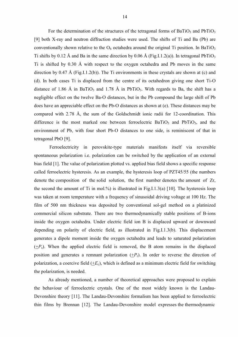
For the determination of the structures of the tetragonal forms of BaTiO3 and PbTiO3
[9] both X-ray and neutron diffraction studies were used. The shifts of Ti and Ba (Pb) are
conventionally shown relative to the O6 octahedra around the original Ti position. In BaTiO3
Ti shifts by 0.12 Å and Ba in the same direction by 0.06 Å (Fig.I.1.2(a)). In tetragonal PbTiO3
Ti is shifted by 0.30 Å with respect to the oxygen octahedra and Pb moves in the same
direction by 0.47 Å (Fig.I.1.2(b)). The Ti environments in these crystals are shown at (c) and
(d). In both cases Ti is displaced from the centre of its octahedron giving one short Ti-O
distance of 1.86 Å in BaTiO3 and 1.78 Å in PbTiO3. With regards to Ba, the shift has a
negligible effect on the twelve Ba-O distances, but in the Pb compound the large shift of Pb
does have an appreciable effect on the Pb-O distances as shown at (e). These distances may be
compared with 2.78 Å, the sum of the Goldschmidt ionic radii for 12-coordination. This
difference is the most marked one between ferroelectric BaTiO3 and PbTiO3, and the
environment of Pb, with four short Pb-O distances to one side, is reminiscent of that in
tetragonal PbO [9].
Ferroelectricity in perovskite-type materials manifests itself via reversible
spontaneous polarization i.e. polarization can be switched by the application of an external
bias field [1]. The value of polarization plotted vs. applied bias field shows a specific response
called ferroelectric hysteresis. As an example, the hysteresis loop of PZT45/55 (the numbers
denote the composition of the solid solution, the first number denotes the amount of Zr,
the second the amount of Ti in mol.%) is illustrated in Fig.I.1.3(a) [10]. The hysteresis loop
was taken at room temperature with a frequency of sinusoidal driving voltage at 100 Hz. The
film of 500 nm thickness was deposited by conventional sol-gel method on a platinized
commercial silicon substrate. There are two thermodynamically stable positions of B-ions
inside the oxygen octahedra. Under electric field ion B is displaced upward or downward
depending on polarity of electric field, as illustrated in Fig.I.1.3(b). This displacement
generates a dipole moment inside the oxygen octahedra and leads to saturated polarization
(+Ps). When the applied electric field is removed, the B atom remains in the displaced
position and generates a remnant polarization (+Pr). In order to reverse the direction of
polarization, a coercive field (+Ec), which is defined as a minimum electric field for switching
the polarization, is needed.
As already mentioned, a number of theoretical approaches were proposed to explain
the behaviour of ferroelectric crystals. One of the most widely known is the Landau-
Devonshire theory [11]. The Landau-Devonshire formalism has been applied to ferroelectric
thin films by Brennan [12]. The Landau-Devonshire model expresses the thermodynamic

15
FIG.I.1.3. Ferroelectric hysteresis loop of PZT45/55 film (d=500 nm) measured with the frequency of driving signal of 100 Hz. The film was fabricated on platinized silicon substrate via conventional sol-gel method [10] (a); polarization reversal due to displacement of cation inside oxygen octahedra (b) [6].
properties of ferroelectric material in terms of the polarization, which serves as the Landau
order parameter. A detailed model of the theory, taking into account nonhomogeneities of
polarization, stresses and electrostrictive effects is rather complex, although, for the first
simple examination of ferroelectric properties, the contribution of stress and electrostrictive
effects can be omitted. Furthermore, since the lowest energy of the system is considered,
saddle point approximation can be used [12]. Further, the uniform polarization of each
domain is assumed. The resulting expression is a simple polynomial free energy function of
polarization:
2 4 61 1 1( )2 4 6
F P P P Pα β γ= + + (I.1.3)
where F is the free energy of the system, P is polarization, α, β and γ are Landau coefficients.
The relation between the electric field and the polarization is given by the derivative of the
free energy expression:
3 5dFE P P PdP
α β γ= = + + (I.1.4)
This expression for the electric field can be used in conjunction with the Poisson
equation fρ∇ =D (where D is the dielectric displacements and ρf is the density of charged
defects) to derive the contributions of charged defects to the local field and hence its influence
-300 -200 -100 0 100 200 300
-40
-20
0
20
40
-Ec
+Ec
-Pr
+Pr
-Ps
P,
µC
/cm
2
E, kV/cm
100 HZ+Ps
(a)
Polarization up
Polarization down
(b)

16
on the structure of the nearby domains [12]. The electric displacement induced by charged
defects can be related to the electric field and polarization by the following familiar equations:
( ) ( )0
0 0
1 1f b
ε
ρ ρε ε
= +
∇ = ∇ − ∇ = +
D E P
E D P (I.1.5)
where ρb is the charge density due to the polarization of the ferroelectric lattice.
By expressing the polarization as a function of electric field the hysteresis of a single
domain, single crystallite can be found. This gives a complex function if we use all terms of
Landau expression. However, using only the two first terms of (I.1.4), a useful expression can
be obtained. 3( )E P P Pα β= + (I.1.6)
This expression describes a simple bistable system which manifests the properties of
hysteresis and coercivity. The inverse roots of expression (I.1.6) are straightforward to obtain.
There are three roots, but only one of them is necessary to plot the real part of the polarization
function. The real-valued
3 2
1 3 233 2
3 2
( )2 27 4
32 27 4
E EP EE E
α αβ β β
αββ β β
= − + + +
+ +
(I.1.7)
portion of this root forms one half of the hysteresis loop of the polarization vs. electric field.
The return trace of the hysteresis is found by reflecting this function about the origin. Fig.I.1.4
shows the polarization hysteresis of single domain (or single crystalline which is in
monodomain state) [12].
This simplified model provides the two characteristics of the ferroelectric that are most
important for device application: remnant polarization and coercive field. However, we must
note that processes related to real material behaviour like domain walls pinning, preferred
domain configuration i.e. imprint, conductivity are out of consideration.
A thin ferroelectric film consists of many domains, which generally exhibit a
distribution in their polar response [12]. The crystallites in a polycrystalline film will have a
certain distribution in their orientation with respect to the electrodes, depending on the type of
material and its microstructure. Those crystallites that are misaligned with respect to the field
will be harder to switch than those that are more closely aligned, and this creates a distribution

17
FIG.I.1.4. Polarization vs. electric field for the case of single domain [12].
of the effective coercive field among the collection of domains. Obviously, the distribution
will be related to the number of allowed polarization directions in the lattice. For example, in
the case of PbTiO3-PbZrO3 solid solution, depending on Zr to Ti ratio the number of allowed
directions changes from 6 for Ti rich “tetragonal” compositions to 8 for Zr rich
“rhombohedral” compositions. Thereby, the maximum number of directions is 14 which is
peculiar to the MPB composition (PZT 52/48 at room temperature) where these two phases
coexist. Distributions in the coercive voltage and remnant polarization can be also caused by
pinning effects due to charged defects. Charged defects, defect dipoles and space charges may
also create built-in fields that cause offsets in the polar response. For example the hysteresis
loop of PZT45/55 ferroelectric film presented in Fig. I.1.3(a) is very similar to that given by
Brennan [12] for a collection of identical domains, each obeying the Landau hysteresis
function (I.1.7), but have a Gaussian distribution of offset voltages due to charged defects.
The distribution of the offset voltages transforms the abrupt hysteresis function of the single
domain into the “soft” hysteresis loop usually observed in the case of ferroelectric thin films.
It is expected that real ferroelectric devices would have a distribution of all relevant
parameters, including coercivity, remanence and offset. In the case of particularly large built-
in fields due to trapped charges and defect dipoles, the offset potentials may exceed the
coercive field of the domain, and the domain will have negative apparent coercive voltage
[12]. In other words, the offset for particular domain may be large enough to force it into a
preferred polarization state in the absence of an applied field. In some cases this process can
be detrimental for functional properties of ferroelectric thin-film devices.
P
E1-1
1
-1

18
I.2. Phase transitions in ferroelectric materials.
Another important characteristic of ferroelectrics is the phase transition from the
paraelectric (cubic) state to the ferroelectric (tetragonal/rhombohedral) state which occurs at a
characteristic temperature called the Curie point TC [p.11 in ref. 8]. When the temperature is
in the vicinity of the Curie point, thermodynamic properties (such as dielectric, elastic,
optical, and thermal properties) of the ferroelectric materials show anomalies as the structure
of the crystalline material changes. For example, the dielectric constant in most ferroelectric
crystals has a very large (abnormal) value (up to 104-105) [p.12 in ref. 8] near their Curie
points. This phenomenon is usually called “dielectric anomaly” and considered to be the basic
feature of ferroelectric materials.
The Landau-Devonshire thermodynamic approach describes the paraelectric-to-
ferroelectric phase transition in terms of phase stability in the vicinity of transition
temperature. For further discussions, Landau power series (I.1.3) must be rewritten taking into
account that the coefficients α, β and γ are temperature dependent [13]:
2 4 61 1 1( , ) ( ) ( ) ( )2 4 6
F T P T P T P T Pα β γ= + + (I.2.1)
Equilibrium value of polarization, P0, at fixed temperature, T, is the value at which the free
energy of the system is minimum. In the absence of an external electric field, the stability
condition of F with respect to infinitesimal change of P is
0
0P
FP
∂ = ∂ (I.2.2)
or, considering (I.2.1),
2 40 0 0( ( ) ( ) ( ) ) 0P T T P T Pα β γ+ + = (I.2.3)
The solution P0=0 of the equation (I.2.3) corresponds to the paraelectric phase. Another
solution, P0≠0, exists only under certain conditions. In fact, not any solution of (I.2.3) is
stable. The stable solution can be found if
0
2
2 0P
FP
∂ > ∂ (I.2.4)
The second derivative of the free energy with respect to polarization is the reciprocal of the
isothermal dielectric susceptibility χT-1. In the presence of an external electric field
dF EdP
= (I.2.5)
and the stability condition (I.2.4) can be expressed as
19
0
21
2 0TP
F dEP dP
χ − ∂ = = > ∂ (I.2.6)
Using (I.2.1), (I.2.6) can be rewritten as follows:
1 2 40 0( ) 3 ( ) 5 ( ) 0T T T P T Pχ α β γ− = + + > (I.2.7)
In the temperature range where the paraelectric phase is stable, P0=0 and inequality (I.2.7)
becomes
1 ( ) 0T Tχ α− = > (I.2.8)
In other words, α(T) must be positive at high temperature for the paraelectric phase to be
stable and χT-1 must tend to zero at the boundary of stability of the paraelectric phase, T0.
Hence, α(T) can be expanded in a Taylor series in |T-T0| in the vicinity of T0. Taking only the
first-order term, we have
0
0( ) '( )
' 0T T
T T TddT
α ααα
=
= −
= > (I.2.9)
Consequently, equations (I.2.8) and (I.2.9) bring us to the Curie-Weiss law for dielectric
susceptibility of the paraelectric phase [13]:
0
0
1'
TC
T T
C
T T
χ
α
=−
=
>
(1.2.10)
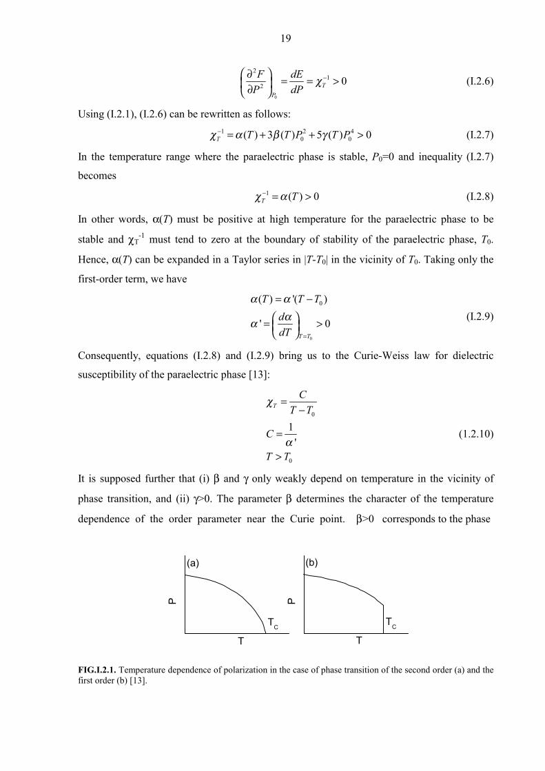
It is supposed further that (i) β and γ only weakly depend on temperature in the vicinity of
phase transition, and (ii) γ>0. The parameter β determines the character of the temperature
dependence of the order parameter near the Curie point. β>0 corresponds to the phase
FIG.I.2.1. Temperature dependence of polarization in the case of phase transition of the second order (a) and the first order (b) [13].
P
T
TC
(a)
P
T
TC
(b)

20
transition of the second-order while at β<0 a first-order transition takes place. In the case of a
first-order transition, the polarization drops abruptly at TC, whereas for a second-order
transition P changes continuously as function of temperature (Fig.I.2.1). First-order transition
is shown by BaTiO3 and PbTiO3. Triglycine sulphate is an example of material which
undergo second-order phase transition. Detailed discussions of the first and second order
phase transitions can be found in a number of textbooks (see, e.g., ref’s 8 (pp.16-24) and 13
(pp.36-46)).
I.3. Properties of some well known ferroelectric materials.
The first material of perovskite structure for which the phenomenon of ferroelectricity
was reported is barium titanate (BaTiO3) [14]. More thorough investigations of oxygen-
octahedron-based materials have resulted in the discovery of ferroelectricity in PbTiO3,
KNbO3, KTaO3, NaNbO3, NaTaO3, PbZrO3, PbHfO3, LiNbO3 and LiTaO3 (p. 103 in ref. 8).
Among these compounds PbTiO3, PbZrO3 and solid solution (PbZrO3-PbTiO3) PZT became
the most popular from the applied point of view due to high ferroelectric, pyroelectric and
piezoelectric characteristics and relatively simple processing and handling procedures.
FIG.I.3.1. PbTiO3-PbZrO3 subsolidus phase diagram [p. 109 in ref. 8]. PC, AT, AO, FR(H), FR(L) and FT denote paraelectric cubic, antiferroelectric tetragonal, antiferroelectric orthorhombic, ferroelectric rhombohedral (high temperature), ferroelectric rhombohedral (low temperature) and ferroelectric tetragonal phases, respectively.
Lead titanate (PbTiO3) is a ferroelectric with a high Curie temperature (490°C) at
which the phase transition from the cubic paraelectric phase to the tetragonal ferroelectric
phase occurs. At room temperature, the structure of PbTiO3 has a symmetry of the point group
4mm with the ratio of axes (tetragonality) c/a = 1.063. From the ferroelectric hysteresis loop
of a PbTiO3 single crystal, a spontaneous polarization of 52 µC/cm2 and a coercive field of

21
6.75 kV/cm are known [p.105-106 in ref. 8]. When Ti+4 ions in PbTiO3 are partially replaced
by Zr+4 with a molar ratio x, a solid solution of xPbZrO3-(1-x)PbTiO3 (0<x<1) binary system
is formed. This solid solution is called lead zirconate titanate (PZT), and its chemical formula
is Pb(ZrxTi1-x)O3. PZT has the perovskite structure with Ti+4 and Zr+4 ions occupying B-sites
at random. Fig.I.3.1 is the T-x phase diagram of the PZT pseudo-binary system, where the
TC-line is the boundary between the cubic paraelectric phase and the ferroelectric phase. A
morphotropic phase boundary (MPB) separates the tetragonal phase region (on the Ti-rich
side) from the rhombohedral phase region (on the Zr-rich side). At room temperature, the
boundary is at the point Zr/Ti=52/48. In the region where Zr/Ti lies between 100/0 and 94/6,
the solution is an antiferroelectric. Zr-rich (rhombohedral) area is also divided by low and
high temperature rhombohedral phase, which both are ferroelectric. The lattice parameters of
PZT are plotted against composition x in Fig.I.3.2 [p.109 in ref.8]. An abrupt change in the
lattice parameters of PZT occurs near the composition corresponding to MPB, where some
physical properties, such as dielectric constant, and piezoelectric electromechanical coupling
factor, show maxima.
FIG.I.3.2. Lattice parameters at room temperature for the PbTiO3-PbZrO3 system [p. 109 in ref.8].

22
II. Methods for ferroelectric thin films processing
In the present section, a short presentation of the most widely used thin film
processing routes is made. The review of different methods of ferroelectric thin films
deposition can be found in textbooks (see, for example ref’s 15,16).
II.1. Electron beam evaporation.
This technique has been used mainly for high temperature superconducting oxide thin
films [16-18], where it has typically been implemented by using individual thermionically
produced electron beams, which are accelerated through 5-10 keV potential, magnetically
deflected, and then focused onto spatially separated elemental targets located in water-cooled
holders symmetrically positioned in front of the substrate. Process parameters, particularly
precise film stoichiometry and sharp interfaces, are difficult to control, since direct sputtering
of individual beams near each source is difficult without disturbing the focused electron
beam. The evaporation of the elemental material from different spatial locations involves
complex hardware and tends to produce nonuniform films across large-area substrates.
II.2. Pulsed laser deposition (PLD).
This method has been extensively used by many groups to produce multicomponent
oxide thin films since the first demonstration of the technique for the production of
superconducting YBa2Cu3O7-x films by ablation of material from sintered YBa2Cu3O7-x
[16,19,20]. The impact of a laser beam (generally an excimer laser with wavelength of 248 or
193 nm) on the target, produces localized melting and resolidification that for some target
materials results in topographical and compositional changes of the impacted area of the
target, which affects the reproducibility of the film characteristics after several hundred
pulses. The problem is solved by continuous rotation of the target and/or laser beam scanning
on the surface to permanently expose a fresh area to the laser beam.

23
For the synthesis of ferroelectric PZT, initial work on laser ablation from continuously
exposed fresh areas of a PZT target demonstrated the feasibility of producing deposited films
at substrate temperatures of 500-600°C, and in oxygen atmospheres, needed for nucleation of
the perovskite PZT film [16,21]. However, even in the presence of a seemingly appropriate
oxygen atmosphere, early as-deposited PZT films contained a pyrochlore phase [16,22],
possibly due to Pb deficiency in the film. Furthermore, PLD is particularly not suitable for
large-area deposition.
II.3. Multi-ion-beam reactive sputter deposition (MIBRSD).
The basic idea of the MIBRSD technique is that individually mounted single-
component targets are sputtered independently yet simultaneously by different ion sources, so
that a highly controllable deposition process can be achieved [p. 429 in ref. 16]. Such
technique, as can be expected, is rather complicated in instrumentation and requires a series of
adjustments, modulations and calibrations. Since different single-element targets are sputtered
individually by independently operated ion sources, the MIBRSD allows the utmost capability
of varying and controlling the composition of deposited films.
II.4. Organometallic chemical vapour deposition (OMCVD).
Chemical vapour deposition processes (CVD), where volatile compounds of the
elements to be incorporated into the solids, the so-called precursors, are transported via the
gas-phase to the region where deposition takes place, are well known [p. 485 in ref. 16].
Historically, the most commonly used precursors are chlorides and hydrides. Such
compounds are readily available, in most cases easy to handle and often have sufficiently high
vapour pressures. Although, good results are usually obtained, process control is not always
optimal and the contamination of the films with halogen ions is reported. To overcome this
drawback the use of an alternative class of precursors – organometallic compounds (see
below) was proposed [16,23].
Due to the advantages of this new type of precursors, such as lower temperature of
decomposition, higher volatility as compared to the traditional sources, the OMCVD method
allowed the fabrication of high quality, high temperature superconducting (HTSC) and
ferroelectric materials in the form of thin films. OMCVD is a technique allowing direct
formation of thin films in the proper crystalline phase and even epitaxial films for lattice

24
matched substrates. It has the advantage over most other techniques that a high oxygen partial
pressure can be applied during the deposition. OMCVD can be easily scaled-up, both in wafer
throughput as well as in wafer diameter. This makes the technique a promising candidate for
deposition on an industrial scale. However, the technique involves high investment and
operating cost.
II.5. Sol-gel processing of thin films.
Among the chemical deposition methods the sol-gel processing route have earned
great attention [24] for coatings, fibres, ultrafine and ultrapure powders and bulk materials
fabrication. Being firstly utilized by Budd et al. [25] for ferroelectric thin films deposition,
e.g. PbTiO3, PbZrO3, Pb(Zr,Ti)O3 and (Pb,La)(Zr,Ti)O3, the sol-gel method remains until
now the method of choice for ferroelectric coating fabrication [26]. Analysis of the
publications on ferroelectric thin films processing shows that the sol-gel method is the leading
and most accessible one as compared to other physical and epitaxial (i.e. metalorganic
chemical vapour deposition OMCVD) methods. High quality ferroelectric and relaxor thin
films of different compositions are successfully obtained by sol-gel [27-32]. Unlike physical
FIG.II.5.1. Generalized flow chart diagram of sol-gel process.
deposition methods mentioned above, the sol-gel route does not require sophisticated and
expensive equipment; on the other hand it provides suitable stoichiometric control that is very
important for the fabrication of oxides of complex stoichiometry such as perovskite
Precursor sol
Gelation
Drying
Sintering
Coatings
Powder
Fibers
Monoliths
25
ferroelectrics. Many definitions of the sol-gel process have been proposed. One of them is
“Sol-gel is the process of production of inorganic oxides either from colloidal dispersion or
from metal alkoxides”. This definition has been introduced by Segal [33]. Although
developments of sol-gel include now also the promising field of hybrid organic-inorganic
materials [34], the definition of Segal is valid in the case of ferroelectric fabrication, where
alkoxides are the basic reagents, and can be accepted in this work. Alkoxides are compounds
with generalized chemical formula M(OR)n. They are obtained from direct or indirect
reactions between a metal M and an alcohol ROH. As an example the titanium alkoxides
Ti(OC2H5)4 (titanium ethoxide), Ti(OC3H7)4 (titanium isopropoxide) and Ti(OC4H9)4
(titanium butoxide) which can be used for TiO2 or titanate fabrication can be mentioned . An
exhaustive review on the history and chemistry of alkoxides can be found elsewhere [pp. 233-
327 in ref. 16].
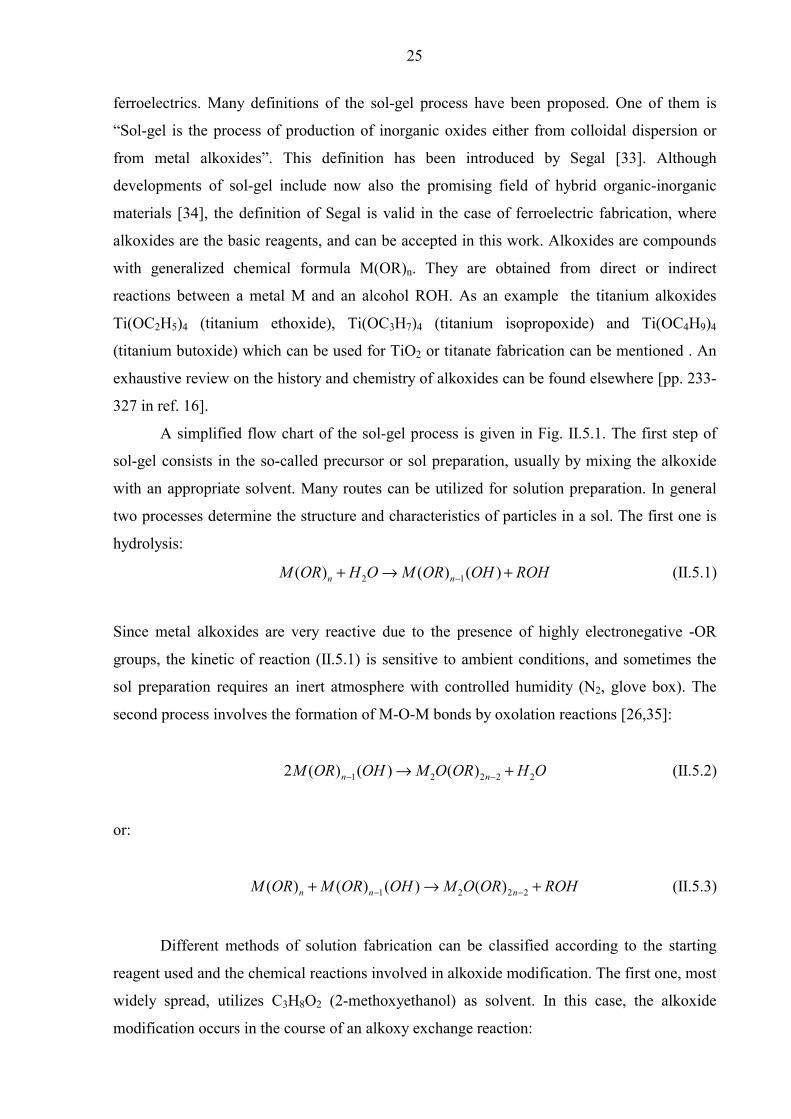
A simplified flow chart of the sol-gel process is given in Fig. II.5.1. The first step of
sol-gel consists in the so-called precursor or sol preparation, usually by mixing the alkoxide
with an appropriate solvent. Many routes can be utilized for solution preparation. In general
two processes determine the structure and characteristics of particles in a sol. The first one is
hydrolysis:
2 1( ) ( ) ( )n nM OR H O M OR OH ROH−+ → + (II.5.1)
Since metal alkoxides are very reactive due to the presence of highly electronegative -OR
groups, the kinetic of reaction (II.5.1) is sensitive to ambient conditions, and sometimes the
sol preparation requires an inert atmosphere with controlled humidity (N2, glove box). The
second process involves the formation of M-O-M bonds by oxolation reactions [26,35]:
1 2 2 2 22 ( ) ( ) ( )n nM OR OH M O OR H O− −→ + (II.5.2)
or:
1 2 2 2( ) ( ) ( ) ( )n n nM OR M OR OH M O OR ROH− −+ → + (II.5.3)
Different methods of solution fabrication can be classified according to the starting
reagent used and the chemical reactions involved in alkoxide modification. The first one, most
widely spread, utilizes C3H8O2 (2-methoxyethanol) as solvent. In this case, the alkoxide
modification occurs in the course of an alkoxy exchange reaction:

26
( ) ' ( ')n nM OR nR OH M OR nROH+ → + (II.5.4)
here -OR' is the methoxyethoxy group. The resultant methoxyethoxide M(OR')n is usually
more stable and less sensitive to water.
The “hybrid” or “chelate” process uses other reagents for alkoxide modification by the
chelating reaction:
3 3( ) ( ) ( )n n x xM OR xCH COOH M OR OOCCH xROH−+ → + (II.4.5)
Although as a chelating agent acetylacetone [36] or acetic acid [37,38] are usually used, 2-
methoxyethanol can be utilized as a final solvent and agent controlling concentration and
rheology of the solution.
Further growth of sol species, which are oligometric in nature, according to processes
similar to (II.5.2) and (II.5.3) leads to the gelation of the sol. This is the next step of sol-gel
processing (see Fig. II.5.1). A gel is a porous 3-dimensionally interconnected solid that
expands throughout a liquid, and is limited only by the size of the container. The gel must
then be dried at moderate temperatures to evaporate the solvent. Depending on conditions and
technology of gelation and drying, powders, monoliths, coatings or fibers can be formed. In
the case of thin film processing, spin-coating, dip-coating or spray-pyrolysis routes are
usually utilized for thin dense layer formation. The final product is annealed at high
temperature (but not higher than 1000°C) in order to complete phase transformation.

27
III. Applications of ferroelectric thin films
In this section some outstanding application potentials for ferroelectric thin films will
be presented and discussed. The applications of ferroelectrics in passive electronic
components such as high power capacitors will not be considered.
III.1. Non-volatile and dynamic random access memories.
As mentioned in the Introduction, the trend towards miniaturization and integration of
electronic devices into the existent semiconductor circuits production technology has been the
main driving force for the development of ferroelectric thin films [39]. The main efforts have
been focussed on the development of non-volatile (NVRAM) and Dynamic Random Access
Memory (DRAM) using ferroelectric thin films based on barium-titanate and lead-zirkonate-
titanate. Barium titanate based non-volatile memory was developed in the early 50’s in the
research laboratories of AT&T, Ford, IBM and Westinghouse [40]. The first storage devices
comprised a 100 mm slice of single crystal BaTiO3 provided with x-y addressed electrode
matrix. An electric field was used to switch the spontaneous polarization, or “write”, each
ferroelectric cell into either positive or negative polarization state. From the perspective of
binary encoding, one polarization state could be regarded as a “1”, and the opposite as a “0”.
Whilst the principle of a ferroelectric memory was demonstrated, the device did not prove
commercially practical because of the crystal being too expensive, excessive cross-talk
between adjacent address lines, and the large write voltage required. With the advent of thin
film ferroelectrics and the introduction of semiconductor architectures [41], non-volatile
random access memories (NVRAM) have now become a commercially viable option.
Dynamic random access memory (DRAM) is the most widely used method of
temporary data storage, providing the memory for all personal computers. In its structure it
comprises a transistor connected to an integrated capacitor. A binary state is stored by
maintaining a potential on the capacitor but, because the capacitor discharges, its voltage is
refreshed several times per second. Since ferroelectric materials typically show large
dielectric constants, ferroelectric thin films have been considered as strong candidates for high

28
density DRAM applications. As the density of DRAM increases over 1 Gbit, the cell size is
tremendously reduced, so that the current SiO2 dielectric layer is regarded as impractical due
its low dielectric constant of typically 4. Practically the charge storage capability can be
improved either by increasing the capacitive area or the dielectric constant for a given
dielectric layer thickness. However, in conventional DRAM most of the space is occupied by
the capacitor, therefore in order to reduce cell size the area of the capacitor must be decreased.
Therefore, the search for high-permittivity thin films is a reasonable choice. Since most of the
commonly used ferroelectrics have dielectric constants at least two orders of magnitude
higher than that of SiO2, ferroelectric thin films can be used as non-switching capacitor
materials in high density DRAM devices. Some excellent work on the application of
ferroelectric thin films for memory devices fabrication has been published [42 and references
therein]. An exhaustive description of materials and device issues in the application of
ferroelectric thin films for memory devices can be found in the monograph of Scott [15].
III.2. Microelectromechanical systems.
Microelectromechanical systems (MEMS) combine traditional Si-integrated circuit
(IC) electronics with micromechanical sensing and actuating components. According to [43],
the term MEMS has become synonymous for many types of microfabricated devices such as
accelerometers, flow-meters, micro-pumps, motors and mechanical components. The ultimate
goal of MEMS is a self-contained system of interrelated sensing and actuating devices
together with signal processing and control electronics on a common substrate, most often Si.
Since fabrication involves methods common to the IC industry, MEMS can be mass-
produced. Commercial applications of MEMS already span biomechanical, manufacturing,
information processing, and automotive industries. More applications are projected in
consumer electronics, manufacturing control, communications, and aerospace. Ferroelectric
materials have many properties desirable for MEMS applications. The strong piezoelectric
effect allows electromechanical sensing and actuation. The spontaneous charge induced from
mechanical strain in ferroelectric thin films is easily sensed across a capacitor structure using
a voltage- or charge-sensitive amplifier. Direct and converse piezoelectric effects in
ferroelectric materials are expressed as [6]:
'TD dT Eε= + (III.2.1) ES s T dE= + (III.2.2)

29
where D is the dielectric displacement, T the stress, S the strain, d the piezoelectric
coefficient* and s the material compliance (inverse of modulus of elasticity). The direct effect
(III.2.1) is identified with the phenomenon whereby electrical charge (polarization) is
generated from a mechanical stress, whereas the converse effect (III.2.2) is associated with
the mechanical movement generated by the application of an electrical field. The superscripts
in (III.2.1) and (III.2.2) indicate the quantity held constant: in the case of ε′T, the stress is held
constant, which means that the piezoelectric element is mechanically unconstrained, and, in
the case of SE, the electric field is held constant, which means the electrodes on the elements
are shorted together.
Electrostriction is another electromechanical effect which can be exploited for MEMS
application. In electrostriction, the sign of the deformation that occurs as a result of an applied
electric field is independent of the polarity of the field [6], and the value of deformation has a
quadratic dependence on the applied field (in piezoelectricity, the deformation is linear with
respect to the applied field and changes sign when the field is reversed). The corresponding
equation in terms of electric field is:
2S mE= (III.2.3)
and in terms of polarization:
2S QP= (III.2.4)
where m and Q are corresponding electrostrictive coefficients.
Although electrostriction is a general property of all dielectric materials, whether they
are crystalline, amorphous, polar, or centrosymmetric, it can be particularly large in
ferroelectric materials just above their Curie point, where an electric field can enforce the
energetically unstable ferroelectric phase. More commonly this effect is utilized to good
advantage in relaxor materials, such as lead magnesium niobate (PMN), lead zinc niobate
(PZN), and lead lanthanum zirconate titanate (PLZT). Electrostrictive materials can be
operated either in the electrostrictive mode (as stated above) or in the field-biased
piezoelectric mode [6]. Device design for electromechanical applications typically includes a
thin, flexible structural material covered with the ferroelectric thin film sandwiched between
metal electrodes.
* In general, since piezoelectric coefficient is a second-rank tensor vlaue, it is corerct to write d in the equations (III.2.1) and (III.2.2) as the tensor components; in the case of polycrystalline thin films we are talking about the effective value of piezoelectric coefficient, deff. Notation d33 is also used sometimes to represent piezoelectric coefficient measured in the direction perpendicular to film surface.

30
III.3. IR detectors.
IR (infrared) detector arrays and IR cameras play an extremely important role in
military and civil applications [44]. Infrared imaging systems have been used for 30 years to
provide operational capability in the dark of the night. Traditional night vision systems have
been large and costly, and their use has been therefore restricted to aircraft and heavy
platforms. Today photon (quantum) detectors in combination with mechanical scanning
technique are widely used for these night vision systems. Photon detectors convert absorbed
IR radiation directly into an electrical signal. These detectors can be quite sensitive, but need
to be cryogenically cooled in order to suppress their noise mechanisms. Until recently, these
FIG.III.3.1. Scheme of the integrated ferroelectric thin film based pyroelectric detector. Inset shows voltage response to 20 mW incident IR signal.
detectors were considered only for military applications. This situation is completely different
for civilian and commercial applications. There is a large potential for application of IR
detectors and cameras, which can include surveillance of buildings, the detection and fire-
fighting, and night driving assistance. IR detectors and cameras could have a large impact in
these areas if their costs can be reduced considerably. Alternatively to IR photonic detectors a
cheap technology makes use of the pyroelectric properties inherent to ferroelectric ceramics
and thin films. The latter can be easily incorporated into the silicon circuit as exemplified in
Fig.III.3.1. For these films, there is no need for cooling and they do not show spectral
31
dependence [44]. The absorbed IR radiation results in a temperature change of the detector
elements, which in turn leads to an electrical response due to the temperature dependence of
the spontaneous polarization of the detector material (pyroelectric effect). Dielectric
displacement D in ferroelectric materials is given by the equation
0' sε ε= +D E P (III.3.1)
where E, ε′, and ε0 are the external electric field, the dielectric constant and the permittivity of
free space, respectively [45]. Therefore at the constant field
0'Sdd d
dT dT dTεε= +PD E (III.3.2)
and
0'
gddTεε= +p p E (III.3.3)
where
SddT
= Pp (III.3.4)
pg and p are referred as generalized and true pyroelectric coefficients, respectively.
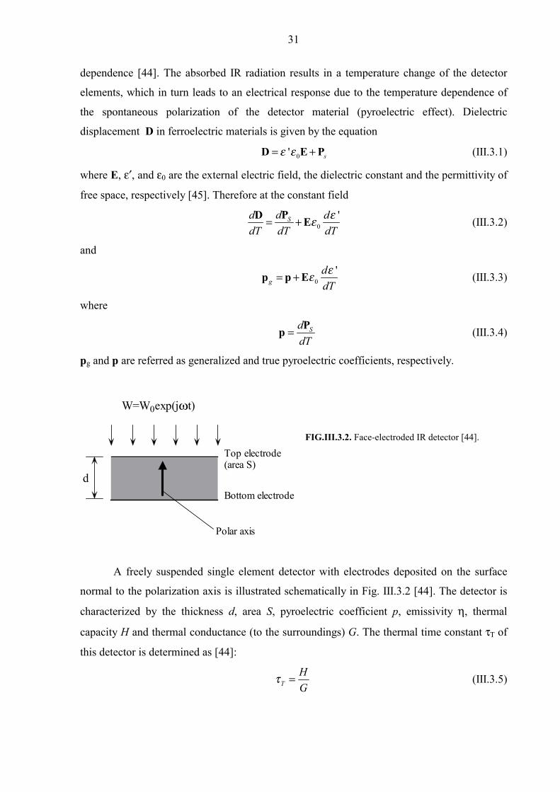
FIG.III.3.2. Face-electroded IR detector [44].
A freely suspended single element detector with electrodes deposited on the surface
normal to the polarization axis is illustrated schematically in Fig. III.3.2 [44]. The detector is
characterized by the thickness d, area S, pyroelectric coefficient p, emissivity η, thermal
capacity H and thermal conductance (to the surroundings) G. The thermal time constant τT of
this detector is determined as [44]:
THG
τ = (III.3.5)
Polar axis
Bottom electrode
Top electrode(area S)
W=W0exp(jωt)
d

32
The element is exposed to a sinusoidally modulated radiation flux with a power density W
(see Fig.III.3.2). The temperature difference between the detector and its surroundings is
expressed as follows:
dTW H GTdt
η = + (III.3.6)
The solution of the equation is:
0 exp( )WT j tG j H
η ωω
=+
(III.3.7)
where j, ω and t are complex operator, angular frequency and time, respectively. Usually the
output of the pyroelectric detector is amplified using current or voltage amplifiers. The
electrical time constant of the detector is determined by the capacitance, CT, and the
resistance, RT, of the circuit and expressed as:
E T TR Cτ = (III.3.8)
It is usually convenient to define quantities such as the current responsivity, RI, which is the
pyroelectric current generated by the detector per watt of input power:
2 2 1/ 20 (1 )p
IT
I pSRW G
η ωω τ
= =+
(III.3.9)
If ω<<1/τT, RI is proportional to ω. At high frequencies, RI is constant and determined by the
thermal and pyroelectric properties of the detector material and detector geometry [44]:
'IpR
c dη= (III.3.10)
The electrical admittance of the detector circuit is:
1T
T
Y j CR
ω= + (III.3.11)
The voltage responsivity (pyroelectric voltage generated per watt of input power) is given by:
2 2 1/ 2 2 2 1/ 20 (1 ) (1 )p T
VT E
V R pSRW G
η ωω τ ω τ
= =+ +
(III.3.12)
The voltage responsivity of the detector is illustrated schematically in Fig. III.3.3. Three
regions in RV(ω) curve can be distinguished. When ω<1/τT, the responsivity is proportional to
the frequency. At high frequency (ω>1/τE) the responsivity is proportional to 1/ω and given
by:
'V
T
pRc dC
ηω
= (III.3.13)

33
In the intermediate frequency range RV(ω) is rather flat and has its maximum at ω=1/(τTτE).
The maximum value of the voltage responsivity is therefore expressed as:
(max)( )
TV
T E
RR pSG
ητ τ
=+
(III.3.14)
Using high IR-absorbing materials as top electrodes (maximising η) and minimising τT by
making the detector thinner (minimising the thermal capacity) and thermally isolating it
(minimising G) can improve the responsivity of certain pyroelectric detector.
FIG.III.3.3. Frequency variation of voltage responsivity of a pyroelectric detector [44].
There are different figures of merit (FOM) of pyroelectric materials which determine
the applicability of the materials under specific conditions. The most important of them are
the current FOM which can be expressed as:
'I
pFc
= (III.3.15)
the voltage FOM:
0' 'V
pFc ε ε
= (III.3.16)
and detectivity FOM:
0' ' tanDpF
c ε ε δ= (III.3.17)
where c′ is the volume specific heat and tanδ is the loss tangent respectively [44,45]. We can
see that the applicability of the material for pyroelectric devices depend on thermal properties,
as well dielectric and ferroelectric properties. A good FOM involves high pyroelectric
coefficient, p, low ε′ and tanδ.
logRV
logω
RV(max)
RV(T)
1/τT 1/τE1/(τTτE)2

34
As already mentioned in the Introduction, the advantage of a thin-film device is that
the material can be directly deposited on the integrated circuit. The same materials which are
actively used for discrete IR detectors fabrication are usually considered for the applications
in thin-film devices. These materials are mainly complex oxides of perovskite (like BaTiO3 or
PbTiO3) and perovskite related (e.g. LiTaO3 or (Sr,Ba)Nb2O6) structures. Lead zirconate
titanate based perovskite-type thin films have become of considerable importance from the
point of view of their potential applications in IR devices and imaging systems due to good
pyroelectric and dielectric properties and relatively low processing temperature. The
properties of PZT of various composition are listed in Table III.3.1 (taken from Wersing and
Bruchhaus [44], p. 185).
Table III.3.1. Dielectric and pyroelectric properties of PZT thin films of different compositions (Wersing and Bruchhaus, [44], p. 185).
PZT film ε′ tanδ p, 10-4 C/m2K p, 10-4 C/m2K (after poling)
PZT(10/90) 172 0.006 2.09 2.02 PZT(20/80) 209 0.007 2.14 2.16 PZT(24/76) 245 0.006 2.12 2.31 PZT(38/62) 539 0.01 1.57 2.50 PZT(44/56) 665 0.014 1.28 2.39 PZT(48/52) 767 0.014 0.33 1.33 PZT(60/40) 598 0.011 0.11 1.24
Furthermore, the performance and properties stability of the active element of the IR
detector are affected by the degree of preferred orientation, material composition and
fabrication conditions. All these factors are even more important in the case of thin films of
sub-micron thickness suspended on the substrate with specific properties and will be
discussed in more details in the following.

35
IV. Characterization of ferroelectric materials
In the present chapter the basics of the methods used for the characterization of the
structural and electrophysical properties of ferroelectrics are briefly described. The
Experimental details will be presented separately in Chapter VII.
IV.1. X-ray diffractometry.
The basics and the theoretical background of the X-ray diffractometry (XRD) can be
found in a number of textbooks (see, for example ref. 46). X-rays are electromagnetic
radiation with typical photon energies in the range of 100 eV - 100 keV. For diffraction
applications, only short wavelength X-rays (hard X-rays) in the range of a few angstroms to
0.1 angstrom (1 keV - 120 keV) are used. Because the wavelength of X-rays is comparable to
the size of atoms, they are ideally suited for probing the structural arrangement of atoms and
molecules in a wide range of materials. The energetic X-rays can penetrate deep into the
materials and provide information about the bulk structure. X-rays are produced by either X-
ray tubes or synchrotron radiation. In an X-ray tube, which is the primary X-ray source used
in laboratory X-ray instruments, X-rays are generated when a focused electron beam
accelerated across a high voltage field bombards a stationary or rotating solid target. As
electrons collide with atoms in the target and slow down, a continuous spectrum of X-rays are
emitted, which are termed Bremsstrahlung radiation. The high energy electrons also eject
inner shell electrons in atoms through the ionization process. When a free electron fills the
shell, an X-ray photon with energy characteristic of the target material is emitted. Common
targets used in X-ray tubes include Cu and Mo, which emit 8 keV and 14 keV x-rays with
corresponding wavelengths of ~1.54 Å and ~0.8 Å, respectively. (The energy E of an X-ray
photon and its wavelength are related by the equation E=hc/λ, where h is Planck's constant, c
the speed of light and λ is the wavelength). Bragg's Law of X-ray diffraction is given by the
following formula:
2 sind nλΘ = (IV.1.1)

36
A monochromatic X-ray beam with a wavelength λ incident onto a crystalline material at an
angle Θ, leads to diffraction when the distance travelled by the rays reflected from successive
planes differs by a complete number n of wavelengths. By varying the angle theta, the Bragg's
Law conditions are satisfied by different d-spacings in polycrystalline materials.
One of the most significant drawbacks limiting the applicability of conventional X-ray
powder diffractometry for the characterization of thin films of submicron thickness is the
contribution of substrate material to XRD spectra due to relatively high penetration depth of
X-rays. Very often diffracted reflections which belong to the substrate material mask the
reflections coming from the film. Moreover, when the specimen consists of polycrystalline
thin film deposited on single crystal or highly textured polycrystalline substrate, the intensity
of the peaks diffracted from substrate can exceed the reflections from the films by many
orders of magnitude. The acquisition of X-ray spectra from thin films using grazing incidence
(GI) adjustment of the diffractometer is one of the possibilities to avoid reflections from
substrate [47]. In this experimental configuration the specimen is aligned in such a way as to
expose the surface of the film to the incident X-ray beam at a very low ("grazing") angle
(usually 1-2°, as illustrated schematically on Fig. IV.1.1) which is kept constant during the
experiment. This increases significantly the path of X-rays within the thin film. The spectra
are obtained by changing the position of the secondary goniometer in the desired range of
angles (2Θ) with appropriate duration and step width.
FIG.IV.1.1. Scheme of grazing incidence XRD experiment.
Texture analysis is another important application of X-ray diffractometry. In view of
the tensor nature of the electrophysical properties, correlation between preferentially oriented
state and dielectric, ferroelectric and piezoelectric properties of ferroelectric polycrystalline
thin films is of crucial importance, and have been thoroughly investigated [48-51]. It has to be
noted that comparison of the spectra obtained in Θ-2Θ configuration for textured and random
(powdered) specimens gives an idea only about out-of-plane (in the case of the films
2Θ
1°-2°
Plane of the filmIncident X-ray beam
DiffractedX-rays

37
perpendicular to the plane of substrate) texture, and in the most of the cases analysis of pole
figures is required to reconstruct the full picture of diffracted intensity distribution with
respect to the plane of the substrate. Exhaustive theoretical background on the application of
X-ray diffractometry and pole figures for texture analysis can be found in textbooks [52-54].
The acquisition of a direct pole figure consists in the registration of the diffracted intensity
distribution around the chosen peak. The situation is depicted on Fig. IV.1.2. The specimen is
fixed at the angular position (Θ-2Θ) corresponding to Bragg conditions of one of the
reflection. Then the specimen is tilted by an angle Chi with subsequent rotation around the
normal to the sample surface (angle Phi). The distribution of the diffracted intensity, usually
plotted in the contour plot form, vs. Phi and Chi is called direct pole figure.
FIG.IV.1.2. Direct pole figure acquisition-scheme of the experiment.
Fibre texture (FT) is usually found for the majority of thin films deposited onto
polycrystalline substrates via sol-gel method (a uniform pole density distribution with respect
to the azimuthal angle, Phi, indicates the fibre or uniaxial character of the texture). Therefore
in the following discussion we will mainly concentrate on the analysis of the FT plots (which
are simply the cross-sections of the corresponding pole figures Phi=const) since the
acquisition of a complete pole figure is rather a time consuming experiment.
IV.2. Raman spectroscopy.
After the inelastic scattering of light (Raman effect) was discovered [55] and laser
technique developed, Raman spectroscopy has become widely used by physicists and
materials scientists for studying excitation processes in solids. Nowadays, a number of
spectrometers is available commercially. The theoretical background is given in standard
textbooks (see, for example ref. 56). Scattering from time-varying structures (vibration of
atoms) is accompanied with conservation of energy:
nChi
Phi
Incident X-ray beam Diffracted X-rays
Plane of the film Chi

38
0 ( ) 0ω ω ω− ± =qh h h (IV.2.1)
where ħ is the reduced Plank's constant, ω0 and ω are frequencies of incident and scattered
light and q is wave vector of the elementary excitation of lattice, i.e. phonon [56]. Usually a
Raman spectrum consists in set of frequencies or bands. Each band corresponds to specific
elementary excitation of lattice. In a Raman spectroscopy experiment, the sample surface is
irradiated with a monochromatic polarized light (usually from Ar- or HeNe-laser). The
scattered light is then registered with an appropriate detector. Since the intensity of
inelastically scattered light is several orders of magnitude weaker than that of elastically
scattered (Rayleigh scattering), up-to-date Raman experiment involves a number of
sophisticated techniques for signal registration and processing. Apart from the investigations
of lattice dynamic processes in solid matter, Raman spectroscopy is actively used in materials
science to analyse the structural properties and quality of surfaces and thin films. For
example, a Raman spectrum is known to be sensitive to the crystallinity (when polycrystalline
specimen is considered) of materials, stresses and surface states. A detailed description of
Raman spectra of tetragonal perovskite ceramics and thin films will be given in the following.
IV.3. X-ray photoelectron spectroscopy.
X-ray photoelectron spectroscopy (XPS) is one of the powerful methods of surface
analysis developed over the past 20 years [56]. In XPS, the specimen is irradiated under ultra-
high vacuum with soft monochromatic X-rays which cause photoionisation of core electrons
of atoms in the specimen. If the photoelectrons have kinetic energies high enough for
overcoming the work function of the specimen, they escape from the specimen surface and
can be collected with an appropriate detector. So-called 127° analyser is often used. Main
parts of this detector are cylindrical sector plates and exit slit. Applying a variable voltages
across the plates allows the electrons with different kinetic energy to pass through the exit
slits (p. 153 in ref. 56). Since the levels of core electrons are quantised, the kinetic energies of
emitted electrons provide information on the chemical composition of the sample
investigated. The kinetic energy Ek of the photoelectron is expressed by Einstein relation
.k bE hv E= − The term hν present incident X-ray energy. Eb is the binding energy which is
equal to the ionisation energy of the electron. Due to strong absorption of the photoelectrons
by the sample material, the escape depth, which is dependent on the kinetic energy of the
photoelectron, usually does not exceed 5 nm. Therefore XPS has become a popular method
for in situ surfaces and thin films analysis. When XPS analysis is accompanied with ion

39
milling it allows depth analysing and profiling of element distribution in near-surface regions
of specimen. As an example, Fig. IV.3.1 illustrates the results of Fe distribution profiling vs.
depth of a PZFNT/PZT pyroelectric bimorph thin film (see ref. 58 for experimental details).
Milling with Ar ions with subsequent XPS investigation and analysis of the intensities of XPS
peaks (2p1/2 and 2p3/2 of Fe on Fig.IV.3.1(a)), has let us to reconstruct Fe distribution profile
in our specimen (Fig.IV.3.1(b)).
FIG.IV.3.1. Dependence of 2p1/2 and 2p3/2 Fe peaks intensity vs. depth of a heterostructure consisting of PZFNT and PZT successive coatings (a), and Fe distribution through thickness of the specimen (painted area shows approximate position of the PZT/PZFNT interface) (b) [58].
IV.4. Scanning electron microscopy.
The standard technique which is used for high resolution imaging of solid surfaces is
now scanning electron microscopy (SEM). Many scanning electron microscopes are
commercially available. In SEM, an electron beam source emits electrons which are then
collected and focused by lenses to form few nanometres sized probes. Deflection coils are
used to operate electron beam and scan sample surface. Simultaneously, another electron
beam runs over a TV monitor screen in a synchronized mode. The image magnification is the
ratio of the scanned monitor range to the scanned sample range, and it is easily controllable by
beam deviation elements. Primary electron beam interacts with the specimen surface in a
complicated manner resulting in different emitted signals (secondary and back scattered
electrons, Auger electrons, cathodoluminescence and X-ray radiation) which could be
registered with the appropriate detector. SEM is a versatile and routine surface
characterization method and is described in standard text books [59].
700705710715720725
Inte
nsity
, a.u
.
B inding energy, eV
2p1 /2
2p3 /2
48 nm64 nm88 nm
112 nm
128 nm
b
0,2
0,4
0,6
0,8
1
1,2
40 60 80 100 120 140
Distance from surface, nm
Fe, n
orm
aliz
ed c
onte
nt
P ZT PZFNT(a) (b)

40
IV.5. Atomic force microscopy.
Over the last years atomic force microscopy (AFM) has become a standard and widely
used technique for surface characterization, readily providing sub-nanometer resolution.
Detailed description of the technique can be found in a number of texts and device manuals
(see e.g. ref’s 60 and 61)). Two main operation modes, viz. contact and non-contact, were
developed and are now available in many commercial devices. In contact mode AFM, a very
sharp tip, mounted on a flexible cantilever (Fig.IV.5.1), is attached to the sample surface. The
sample is scanned under this probe with three-dimensional piezoelectric scanner (scheme
when the cantilever instead of the probe is mounted on the scanner is also realized in some
devices). The deflection of the cantilever is measured using laser beam reflected from
cantilever and position-sensitive photodetector in order to obtain the surface profile or
topography of the specimen (Fig.IV.5.1).
FIG.IV.5.1. Cantilever and photodiode (left) and schematic diagram of contact mode (right) [60].
In non-contact (also called tapping) mode, the cantilever is oscillated at its resonant
frequency at a given distance from the sample (several nanometers) and scanned over its
surface. The system changes the sample (or cantilever) vertical (Z) position to maintain
constant frequency/amplitude of cantilever oscillation. The topography of the surface can be
reconstructed from the vertical (Z) position of the piezoscanner. The phase frequency
variation of the cantilever provides additional useful information about the tip-specimen
interaction and hence sample surface properties. Fig.IV.5.2 exemplifies cantilevers usually
used for contact (silicon nitride, left) and non-contact (silicon, right) AFM modes [61].

41
FIG.IV.5.2. Two types of the cantilevers: silicon nitride (left) and silicon crystal (right) (SEM micrographs) (p. 2-11 in ref [61]).
IV.6. Ellipsometry.
Ellipsometry is a powerful method for high precision measurements of optical
properties and thickness of thin films. Ellipsometry is based on the reflection of light from a
surface [62]. It is supposed that the incident plane wave moves in the direction suggested in
Fig.IV.6.1, and that this wave is reflected from the surface as shown in the figure. The plane
of incidence is defined as being the plane containing the light beam prior to and after the
reflection. The plane of incidence also contains the normal to the surface. We shell refer to
plane polarized waves that are in the plane of incidence as “p waves” and plane waves
polarized perpendicular to the plane of incidence as “s waves” [62] (Ep and Es are
corresponding components of electric field vector). Suppose that there is the light beam
reflecting at an interface between medium 1 and 2 as shown in Fig. IV.6.2. Some of the light
is reflected and some is transmitted. The Fresnel reflection coefficient r is the ratio of the
amplitude of the reflected wave to the amplitude of the incident one for a single interface. The
Fresnel reflection coefficients are given by
* * * *2 1 1 2 1 1 2 2
12 12* * * *2 1 1 2 1 1 2 2
cos cos cos cos;cos cos cos cos
p sN N N Nr rN N N N
ϕ ϕ ϕ ϕϕ ϕ ϕ ϕ
− −= =+ +
(IV.6.1)
where N1* and N2
* are the complex refractive indices of matter. The superscripts in r refer to
waves parallel or perpendicular to the plane of incidence and the subscript refers to either
medium 1 or medium 2. Many real situations involve multiple interfaces, as it is shown in
Fig.III.6.3 [p. 15 in ref. 62]. The resultant reflected wave is made up of the light reflected
directly from the first interface plus all of the transmissions from the light approaching the
first interface from medium 2. Each successive transmission back into medium 1 is smaller.

42
FIG.IV.6.1. Reflection of a light from a surface. The plane of incidence contains the incoming beam and the outgoing beam as well as the normal to the surface (after Tompkins [62])
FIG.IV.6.2. Reflection and transmission of the light at a single interface [60].
FIG.IV.6.3. Reflection and transmission with multiple interfaces [62].
The addition of thin infinite series of partial waves leads to the resultant wave. The total
reflection coefficients are given by
12 23 12 23
12 23 12 23
exp( 2 ) exp( 2 );1 exp( 2 ) 1 exp( 2 )
p p s sp s
p p s s
r r j r r jR Rr r j r r j
β ββ β
+ − + −= =+ − + −
(IV.6.2)
Surface normalPlane of incidence
Reflecting surface
Ep
Es
ϕ1
ϕ2
Ν1∗
Ν2∗
d
ϕ1
ϕ2
ϕ3
N1*
N2*
N3*

43
where the subscript “23” denotes that the Fresnel coefficient is for the interface between
medium 2 and medium 3. β is the film phase thickness and is given by
*2 22 cosd Nβ π ϕ
λ =
(IV.6.3)
where d is the film thickness.
Referring to Fig.IV.6.1, the phase difference between the parallel component and
perpendicular component of the incoming wave is denoted as ζ1. Further, the phase difference
between the parallel component an perpendicular component of the outgoing wave is denoted
as ζ2. The parameter ∆, called delta or often abbreviated as “Del” is defined as
1 2ζ ζ∆ = − (IV.6.4)
Del, then, is the change in phase difference that occurs upon reflection and its value can be
from zero to 360° [p. 17 in ref. 62].
Without regard to phase, the amplitude of both perpendicular and parallel components
may change upon reflection. |Rp| and |Rs| from equations (IV.6.2) are the ratios of the outgoing
wave amplitude to the incoming wave amplitude for the parallel and perpendicular
components, respectively. We define the quantity of Ψ in such manner that
| |tan| |
p
sRR
Ψ = (IV.6.5)
Ψ then is the angle whose tangent is the ratio of the magnitudes of the total reflection
coefficients. The value of Ψ can be between zero and 90° [p. 17 in ref. 62].
The complex quantity ρ is the complex ratio of the total reflection coefficients such
that
p
s
RR
ρ = (IV.6.6)
The fundamental equation of ellipsometry then is
tan exp( )
or
tan exp( )p
s
j
RjR
ρ = Ψ ∆
Ψ ∆ =
(IV.6.7)
where ∆ and Ψ are the quantities, measured by an ellipsometer.

44
IV.7. Ferroelectric hysteresis characterization.
The Sawyer-Tower measuring technique is an established and accepted method for
characterizing nonlinear devices and remains a standard against which all other measurement
methods are compared. The Sawyer-Tower measuring system utilizes a sense capacitor in
series with the device under test (DUT) and measures the voltage drop across the test sample
as shown in Fig.IV.7.1 [63,64]. On the other hand, up-to-date commercially available devices
(for example, RT6000S Radiant Technologies ferroelectric testing system) utilize another
scheme which is called Virtual Ground System (VGS) for ferroelectric properties
characterization. Unlike classical Sawyer-Tower scheme, in the virtual ground measuring
system the sense capacitor is replaced by the measurement circuit shown in Fig.IV.7.2. In this
configuration, the transimpedance amplifier maintains the RT6000S return terminal at a
virtual ground potential. All of the charge that flows through the sample as a result of the
FIG.IV.7.1. Basic Sawyer-Tower test configuration [64].
FIG.IV.7.2. RT6000S virtual ground mode measuring system [64].
Drive voltages
Device under test
Voltage measurements
Sense capacitor
Back voltage
RT6000S drive
Device under test
Integrator Voltagemeasurement
Transimpedanceamplifier gain stage
RT6000S return

45
applied drive voltage is collected by the integrator circuit. The voltage generated on the output
of the integrator is then measured and translated into the test results that are displayed by
RT6000S software.
In Fig. IV.7.3, the solid black waveform is the normal bipolar drive profile used to
produce hysteresis polarization data; it traverses from zero volts to +Vmax, back through zero
volts to –Vmax, then returns to zero. The dashed waveform (Fig.IV.7.3) is the same as the
normal bipolar but with a 180° phase shift. The normal bipolar profile creates the right-hand
portion of the P vs. V plot first followed by the left-hand portion. The “inverse” bipolar
profile creates the left-hand portion first then the right.
FIG.IV.7.3. Drive voltage profiles [64] (see text).
IV.8. Dielectric properties measurements.
Ferroelectric materials are mainly dielectrics. High dielectric constant (ε′) and loss
tangent (tanδ) are basic characteristics of these materials. For most applications the dielectric
constant and loss tangent are important practical parameters. Suppose a parallel plate
capacitor filled with a dielectric medium. When an alternating electric field E with an angular
frequency ω is applied to this capacitor, an alternating current i flowing through the condenser
plate is given by [p. 38 in ref. 8],
0*i j C Eωε= (IV.8.1)
where j is the imaginary operator, C0 is the capacitance of the parallel plate condenser in
absence of any medium, ω is the angular frequency and ε* the complex permittivity. Because
dielectric loss (including the leakage current) exists in dielectric materials, the dielectric
constant must be written as a complex number:
*( ) '( ) ''( )jε ω ε ω ε ω= − (IV.8.2)
time
Voltage
0
+Vmax +Vmax
-Vmax -Vmax

46
where ε′(ω) and ε′′(ω) are the real and the imaginary parts of dielectric constant, respectively.
The latter represents the dielectric loss. Often, it is more convenient to use tanδ (loss tangent)
instead of ε′′:
''tan'
εδε
= (IV.8.3)
There is a number of techniques for frequency dependent dielectric properties
characterization cited in literature. Brief review on the principles of dielectric measurements
can be found in ref. 8. Up-to-date commercially available bridges cover the frequency range
from 0.01 Hz to approximately 10 MHz. For direct measurements of dielectric constant and
loss tangent in audio frequency range, Schering bridge is commonly utilized. Schering bridge
is shown schematically in Fig. IV.8.1. Alternating voltage is applied to the bridge circuit,
including sample, reference capacitor and resistance. The current through the sample is
balanced by the adjustment variable capacitor and resistance in the opposite shoulder of the
bridge. Accurate measurements of dielectric properties at frequencies higher than 10 MHz is
problematic due to contribution of distributed capacity (p. 40 in ref. 8). Other methods such as
resonant circuit, transmission line, waveguides or resonant cavity were developed for
characterization of dielectric materials in different frequency ranges. The description of
techniques can be found in standard textbooks.
FIG.IV.8.1. Schering bridge.
IV.9. Leakage current measurements.
Leakage current is one of the factors limiting the applicability of ferroelectric thin
films in memory devices. Therefore, leakage current measurement is a very important step
heading toward the improvement of material performance. Voltage step, voltage ramp or
detector
sample referencecapacitor
referenceresistor

47
voltage pulse techniques are used [65]. Following Dietz and Waser [65], if any voltage signal
is applied to a dielectric, the current response will be composed of a polarization contribution
(arising from charges which are stored in the system) and a leakage contribution (composing
charges which are carried from one electrode to another). In order to determine the leakage
current of a dielectric thin film as a function of the applied voltage, J-V, either a voltage ramp
technique or a voltage step technique are often employed. In the latter case, the correct
procedure involves a sufficient charging time and an additional analysis of the discharging
current after short-circuiting the sample. This leads to a separation of the polarization and the
leakage contribution to the current. Recording the J-V characteristics often requires long
measuring times, if the leakage currents are small. It is generally accepted that the voltage-
step technique with sufficiently long charging and discharging times reveals the most accurate
and unequivocal J-V data. A controversy, however, has been raised on the question of the
error which is made by applying the (usually much faster) voltage-ramp technique to record
the J-V characteristics [65]. Voltage pulse technique was developed purposely for testing the
suitability of thin films for DRAM capacitors application. The voltage pulse technique allows
simulation of real memory device operation (for details see ref. 65 and references therein).
IV.10. Determination of pyroelectric coefficient of ferroelectric materials.
Various techniques were developed in the last decades for pyroelectric coefficient
measurement. Exhaustive review of methods of quantitative and qualitative characterization
of pyroelectric properties of ferroelectric materials is given by Lang [66].
The most widely accepted method is based on the measurement of temperature
dependent pyroelectric current (p. 328 in ref. 45). The pyroelectric coefficient is simply
calculated using the equation:
pIp dTS
dt
= (IV.10.1)
where
1 Mp
C
RI IR
= +
(IV.10.2)
here t is time, S is the area of the capacitor, I is the measured current and RM and RC are the
input resistance of the amplifier and the leakage resistance of the specimen, respectively. The
circuit for direct measurement of the pyroelectric coefficient is shown in Fig.VI.10.1.
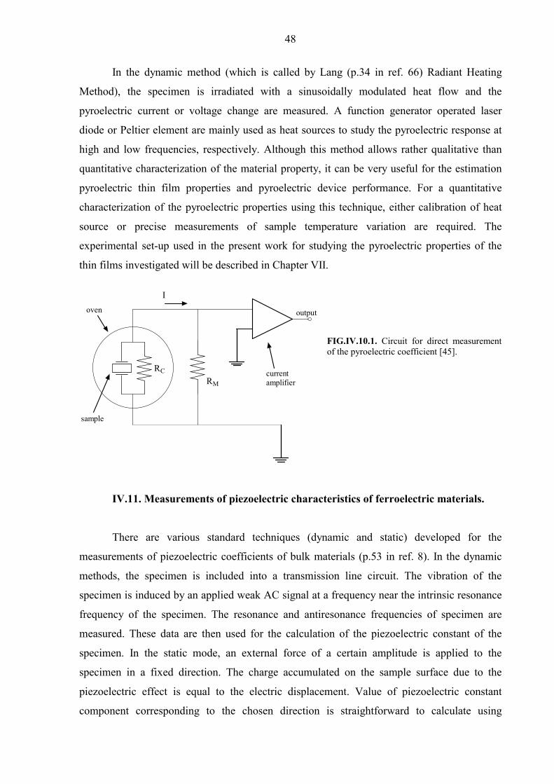
48
In the dynamic method (which is called by Lang (p.34 in ref. 66) Radiant Heating
Method), the specimen is irradiated with a sinusoidally modulated heat flow and the
pyroelectric current or voltage change are measured. A function generator operated laser
diode or Peltier element are mainly used as heat sources to study the pyroelectric response at
high and low frequencies, respectively. Although this method allows rather qualitative than
quantitative characterization of the material property, it can be very useful for the estimation
pyroelectric thin film properties and pyroelectric device performance. For a quantitative
characterization of the pyroelectric properties using this technique, either calibration of heat
source or precise measurements of sample temperature variation are required. The
experimental set-up used in the present work for studying the pyroelectric properties of the
thin films investigated will be described in Chapter VII.
FIG.IV.10.1. Circuit for direct measurement of the pyroelectric coefficient [45].
IV.11. Measurements of piezoelectric characteristics of ferroelectric materials.
There are various standard techniques (dynamic and static) developed for the
measurements of piezoelectric coefficients of bulk materials (p.53 in ref. 8). In the dynamic
methods, the specimen is included into a transmission line circuit. The vibration of the
specimen is induced by an applied weak AC signal at a frequency near the intrinsic resonance
frequency of the specimen. The resonance and antiresonance frequencies of specimen are
measured. These data are then used for the calculation of the piezoelectric constant of the
specimen. In the static mode, an external force of a certain amplitude is applied to the
specimen in a fixed direction. The charge accumulated on the sample surface due to the
piezoelectric effect is equal to the electric displacement. Value of piezoelectric constant
component corresponding to the chosen direction is straightforward to calculate using
sample
RC
RM
I
currentamplifier
outputoven

49
(III.2.1). However, geometrical limitations and inadequate sensitivity make these methods not
applicable for the characterization of the piezoelectric properties of thin films of submicron
thickness. In fact, piezoelectric response (displacement) of such films can be from several
angstroms to several nanometres and fundamentally different techniques must be utilized. The
laser vibrometer technique has been found to be more appropriate for piezoelectric
characterization of thin films. For example, a Doppler heterodyne interferometer was
successfully used [67] for studying the piezoelectric properties of PZT thin films. The device
FIG.IV.11.1. Schematic drawing of the Doppler heterodyne interferometer [67].
exploits the Doppler shift effect. When a sinusoidal voltage is applied across the capacitor, a
sinusoidal displacement
sin( )L L tω= ∆ (IV.11.1)
is induced due to inverse piezoelectric effect. Here ∆L is the displacement amplitude (the
equation is given for the first harmonic). The Doppler frequency shift, fD, is given by the
equation:

50
2D
vfλ
= (IV.11.2)
where v is the velocity of a moving surface and λ is the wave length of light reflected normal
to the surface. The surface velocity and displacement are converted from interferometrically
determined Doppler frequency shift. The Doppler heterodyne interferometer is illustrated
schematically in Fig.IV.11.1 [67]. A 40 MHz acousto-optic modulator (AOM) produces two
beams. One beam is focused at normal incidence on the sample surface and another one is
used as the reference. The sample beam (reflected from the sample surface) and the reference
beam are recombined in a beam splitter before incidence on a photodetector. The intensity of
light arriving at the photodetector is expressed as [67]:
22 cos 2 40r s r svI I I I I MHz tπ
λ = + + +
(IV.11.3)
where Ir and Ip are the intensities of the reference beam and the sample beam, respectively
[67]. Any out-of-plane velocity of the sample surface which relates to the surface
displacement though
vLω∆∆ = (IV.11.4)
where ∆v is the velocity amplitude, produces a corresponding frequency shift in the signal
arriving at the photodetector. The signal from the photodetector is decoded using frequency
modulation (FM) demodulator in the vibrometer controller (Polytec OFV 3001) and then
measured with a digital lock-in amplifier.
51
V. Overview of the properties of lead-based perovskite-type ferroelectric thin films: microstructural and compositional aspects.
The present chapter gives an overview of the electrophysical properties of lead-based
ferroelectric thin films of the perovskite structure. The experimental results reported by other
research groups are discussed with emphasis on microstructural and compositional aspects.
This section is also aimed at the analysis of specific properties of polycrystalline ferroelectric
thin films (not found in bulk materials) such as preferred orientation, development of stresses
due to thermal expansion mismatch between film and substrate materials, as well as thickness
dependence of the dielectric properties.
V.1. Optical properties.
The analysis of publications devoted to the optical characterization of ferroelectric thin
films shows that the topic is of interest from applied and fundamental points of view. The
available literature mainly deals with dimensional effects in the films i.e. dispersion of the,
optical properties vs. thickness and film-electrode interaction. Some results of ellipsometric
and LIMM (Laser Intensity Modulation Method) investigations in PZT thin films can be
found in recent works by Glinchuk et al. [68] and Deineka et al.[69]. Wood et al. [70]
prepared PT, PZT and PMN films and characterised their optical properties with respect to
film thickness and type of substrate. It must be noted that authors could not attain the
complete pyrochlore-to-perovskite transformation probably because of inadequate processing
conditions and the residual pyrochlore was detected for the majority of the specimens
investigated. The results of the refractive coefficients measurements obtained by Wood et al.
[70] are collected in Table V.1.1. Based on extensive experimental data, these authors have
demonstrated that the optical properties of the films are sensitive to both substrate material
and fabrication conditions (in particular, annealing temperature). They also have shown that
the presence of second phase can cause some change in the value of the refractive index.
Wood et al. [70] report that their films are, in general, characterized with lower values of the
refractive indices with respect to those of bulk materials. At the same time, the results are

52
discussed with the emphasis on the waveguiding properties of the films and related
applications which are out of scope of the present work. Moreover, characterization of the
films fabricated utilizing sapphire and single crystalline SrTiO3 as the substrate materials is,
first of all, interesting from the fundamental standpoint. Silicon substrates are required for the
correct discussion of the applicability of the films in up-to-date integrated devices.
It must be pointed out that a systematic investigation of lanthanide elements doping
effects on the optical properties of lead based ferroelectric films is still lacking which is
surprising since firstly, rare-earth elements doping of ferroelectrics is frequently used to tune
their properties, and secondly RE modified materials are of great interest from the point of
view of photonic applications [71]. Doping effects on the optical properties of lead-based
perovskites have been only marginally addressed. Chang and Desu [72] investigated the
dependence of refractive index of La and Nd doped sol-gel fabricated PZT 50/50 thin films
Table V.1.1. Optical properties of PT, PZT and PMN thin films as function of thickness and substrate material (after Wood et al. [70]).
on the concentration of doping elements. It was shown that doping with La and Nd up to 6
mol % results in a small increase in the index of refraction (within 5%). The effect was
attributed to changing in the density o of the films (decreased porosity), and the nature of
dopants was not taken into account. In the present work, the optical properties of sol-gel
deposited PbTiO3 thin films as function of the doping level and atomic number of lanthanide
elements are reported.
Composition Substrate d, nm Refractive index (λ=632.8 nm)
130 2.57 260 2.60
PbTiO3 Sapphire
520 2.55 630 2.25 PZT 60/40 Sapphire 830 2.41
SrTiO3 (100) 280 2.48 SrTiO3 (110) 280 2.50 SrTiO3 (111) 280 2.49
PZT 53/47
SrTiO3 (100) 610 2.50 320 2.33 260 2.45 260 2.48
Sapphire
330 2.28
PMN
SrTiO3 (110) 380 2.46

53
V.2. Microstructure and crystallization kinetics.
The microstructure and phase composition of ferroelectric thin films are known to be
strongly affected by the choice of fabrication route, type of substrate material and deposition
parameters. Epitaxial, preferentially oriented or randomly crystallized films can be obtained
depending on specific processing conditions. The fabrication of epitaxial films requires single
crystal substrates with lattice parameters well matched with those of the film material. On the
other hand, epitaxial growth can be achieved mainly by in-situ deposition methods, such as
PLD or OMCVD. For example, Lee et al. [73] reported on successful deposition of PZT thin
film with composition near the morphotropic phase boundary (MPB), i.e. PZT 52/48 by
means of pulsed laser deposition on MgO (100) crystal. Braun et al. [74] obtained epitaxial
PZT films of different compositions on (1 1 02) oriented sapphire. The sol-gel method allows
the fabrication of textured, or randomly oriented films. Lian and Sottos [67] obtained high
FIG.V.2.1. SEM cross-section of sol-gel fabricated PZT 52/48 (MPB) composition) thin film (after Lian and Sottos [67]).
FIG.V.2.2. SEM cross-section of MOCVD processed tetragonal PZT 35/65 thin film (Ir bottom electrode) (after Kelman et al. [75]).

54
quality (111) and (100) preferentially oriented PZT 52/48 thin films by a sol-gel method on
platinized silicon substrates. Such films usually have columnar morphology (as shown in Fig.
V.2.1) and lateral grain size less than 100 nm. Similar columnar morphology was reported by
Kelman et al. [75] for MOCVD derived tetragonal PZT 35/65 thin film (Fig.V.2.2). An
example of coarse grain formation is shown in Fig.V.2.3 [76]. It seems, that the choice of a
given stoichiometry even within one system of solid solutions (Pb(ZrxTi1-x)O3 or PZT) can
lead to completely different grain morphology, phase compositioncan and textures of sol-gel
processed films.
FIG.V.2.3. SEM cross-section of sol-gel fabricated lead titanate thin film [76].
The morphology of thin films is known to depend on deposition parameters.
Especially, annealing temperature and duration were found to be critical and must be taken
into account in the prediction the final microstructure. In our previous work the effects of
annealing conditions on microstructure of sol-gel PZFNT (Pb1.1(Zr0.58Fe0.2Nb0.2Ti0.2)O3) thin
films have been reported [77]. Based on the results of SEM and XRD characterization it was
shown that not only the microstructure but also the phase composition of the films are
sensitive to annealing conditions. Annealing at 700°C for 20 min resulted in fine crystallized
perovskite phase which was shown to coexist with residual pyrochlore. At higher temperature
(750°C) only perovskite phase was detected. When the annealing time was increased to 30
min pyrochlore phase formation due to PbO volatility was observed. Thus, appropriate
annealing parameters (temperature and duration) lie in a narrow region and must be carefully
optimized. In sol-gel, the desired thickness of the film is usually achieved by multiple
deposition sequences. The thermal history of each layer is critical for the resultant
microstructure of the film. It was reported [78] that using a seed layer (the first layer is
annealed before deposition of the subsequent layers) can significantly affect the morphology

55
of the film. It was concluded that the presence of a seed layer reduces the nucleation energy of
perovskite phase crystallization and promotes the formation of uniform microstructures [78].
The kinetics of thin film crystallization was addressed by many authors. The
theoretical background, including various models of thin film formation can be found in
standard textbooks [79]. In the particular case of perovskite crystallization, nucleation and
growth from an amorphous or pyrochlore phase is supposed to be diffusion controlled. If so,
the crystallization and growth kinetics of perovskite phase particles should obey the Avrami-
type parabolic law [80]:
( ) 1 exp( )nx t Kt= − − (V.2.1)
where x(t) is the crystallized fraction at the time t, K is a temperature dependent constant, and
n is the rate exponent. Values of n were found to be in the range from 0.5 to 1.5 depending on
the annealing temperature for 5 mol % of Nb substituted thin films [80]. The activation
energy of crystallization for these films was found to be169 kJ/mol which lies in the range of
values determined by other authors for crystallization of PZT.
V.3. Raman scattering.
It is appropriate to start the section with a general description of Raman spectra of lead
titanate. Investigations of Raman scattering from PbTiO3 single crystals, powders and thin
films were undertaken by many research groups [81-90]. Systematic studying of Raman
scattering from lead titanate was first reported by Burns and Scott [81,82]. In the paraelectric
phase (above Curie temperature) lead titanate belongs to Oh1 (Pm3m) space group and there
are 12 optical phonons exist. These phonons transforms as the 3T1u+T2u irreducible
representation of the point group. Triply degenerate T2u mode is IR- or Raman-inactive; the
three T1u modes are IR-active. When lead titanate undergoes the paraelectric to ferroelectric
phase transition, Oh1 (Pm3m) space group transforms to the less symmetric tetragonal C4v
1
(P4mm) space group. This reduction of symmetry results in the splitting of three T1u into two
modes transforming as A1+E irreducible presentation of C4v space group. Both A1 and E are
IR- and Raman active [81,82]. In the present work we will use the notation of Burns and Scott
[81,82] for Raman modes. The list of Raman-active modes of lead titanate is given in Table
V.3.1 [84].

56
Table V.3.1. Raman active modes of PbTiO3 lattice below Curie point [84].
TO's are the transverse modes with the polarization perpendicular to the wave vector k
and LO's are longitudinal optical modes with the polarization parallel to k. The two lowest
frequency modes E1(1TO) and A1(1LO) are called "soft modes". A Raman spectrum measured
for sol-gel deposited lead titanate thin films is exemplified in Fig.V.3.1 [90]. B1+E is the so-
called silent mode. All Raman bands reported earlier for bulk materials are present in the
spectrum of the thin film. However, some features peculiar to thin films are found. First, the
Raman spectra obtained for thin films demonstrate noticeable line broadening in comparison
to single crystal; second, the Raman lines are shifted to lower frequencies [84,85]. These
FIG.V.3.1. Raman spectra of sol-gel deposited lead titanate thin films [90].
observations were explained in terms of local disordering of the system and development of
stress during film fabrication [84-86,89]. The frequencies of the phonon modes in a PbTiO3
thin film and PbTiO3 single crystal are compared in Table V.3.2 (ref. 84 and references
therein). Furthermore, it has been reported that the frequency shift of the Raman modes to
lower values (of particular interest is the E(1TO) soft mode because it is responsible for the
ferroelectric to paraelectric phase transition) is caused by small crystallite sizes [83,87] or
doping [88], and is related to lattice tetragonality reduction (induced by the small crystallite
sizes of the film and/or stresses).
A1(3TO) A1(3LO) E(3TO) E(3LO)
A1(2TO) A1(2LO) E(2TO) E(2LO)
A1(1TO) A1(1LO) E(1TO) E(1LO)
Raman shift, cm-1

57
Table V.3.2. Frequencies of the phonon modes in a PbTiO3 thin films and crystals [84].
Frequency (cm-1) Single crystal
Mode pressure ∼0 GPa pressure∼1.4 GPa
Thin film
E(1TO) 89 80 80 A1(1TO) 127 117 116 E(1LO) 128 A1(1LO) 215 E(2TO) 221 200 206 B1+E 290 290 287 A1(2TO) 364 340 341 E(2LO)+ A1(2LO) 445 443 A1(3TO) 508 508 501 E(3LO) 717 ∼720 A1(3LO) 797
V.4. Dielectric properties.
The dielectric properties of thin films can be affected by a number of variables
including processing conditions, substrate materials, phase purity and preferential orientation.
Furthermore, the size effect, i.e. dependence of the dielectric properties on the film thickness
is a specific feature of ferroelectric thin film.
It is quite common for dielectric properties of ferroelectric thin films to be treated
from the point of view of contribution of electrode-film interface(s) into small-signal response
from the film. A number of experimental results published show that the dielectric constant of
the films decreases with film thickness. Paek et al. [91] reported some degradation of
dielectric and leakage properties of BST thin films of thickness ranging from 50 to 300 nm
deposited on platinum electrode. By means of scanning electron microscopy and high
resolution transmission electron microscopy (HRTEM) very thin layer (of thickness between
9.5 and 11 nm) with crystallinity different from that of the bulk of the film was revealed.
Decreasing of the dielectric constant was also reported by Hwang et al. [92] for BST thin
films deposited on platinum electrode. Yet, the dielectric constant of BST films of the same
composition, fabricated on IrO2 bottom electrode was found to be thickness independent in
the film thickness range investigated (from 30 to100 nm). Degradation of the dielectric
properties with decreasing film thickness is also observed by Amanuma et al. [93], Sakashita
et al. [94] and Es-Souni et al. [95]. On the other hand, Shin et al. [96] deny thickness
dependent variation in the dielectric constant of PZT films in the thickness range from 100 to
250 nm processed via sol-gel method on platinized silicon substrate. Thermal expansion

58
mismatch, chemical interaction between materials of the film and bottom electrode lead to the
formation of so-called “dead layer”. This layer has significantly lower dielectric constant and
contains high concentration of defects which, in turn, serve as an effective trap centres for
mobile charges and domain walls. The existence of such layer affects the dielectric properties
of the films especially for very thin films (thinner than 200 nm). It is thought that the
formation of dead layers occurs rather at film-bottom electrode interface than film-top
FIG.V.4.1. Relationship between film thickness and the relative dielectric constant [94]. Experimental results are represented with circles. Solid and broken lines are calculated from a model which assumes that a low dielectric constant layer exists in series with the PZT layer.
electrode interface since the former is exposed to high temperature during film fabrication. An
example of thickness dependent dielectric constant of PZT film, produced by OMCVD on
platinized (100) MgO substrates is shown in Fig.V.4.1 [94]. The structure of the specimen
where low ε′ layer exists in series with bulk part of the specimen is shown schematically on
the inset. These authors also show that microstructure (grain size) and stress state are also
thickness dependent (exhaustive papers on the stress state of lead-based perovskite thin films
are published by Spierings et al. [97] and Sengupta et al. [98]). The survey of literature
reveals that degradation of dielectric properties with film thickness is rather complex. Authors
in [94] suggest 5 possible mechanisms, viz. i) nonstoichiometric phase formation near film-
electrode interface; ii) chemical reaction with platinum electrode; iii) a space-charge layer; iv)
stress and v) the size effect. Yet, Auger electron spectroscopy (AES) depth profiling revealed
rather uniform element distribution of the elements through film thickness. At the same time,
while the results of dielectric and ferroelectric characterization confirm the existence of low
dielectric constant layer in series with bulk of the film, no interaction or interdiffusion among
the PZT film, platinum electrode and MgO substrate were evidenced by means of AES.
Secondary-ion mass spectroscopy (SIMS) also shows similar results. As suggested by Hwang

59
et al. [92] for BST thin films, dielectric constant of the film can decrease with film thickness
even without any interfacial low dielectric constant layer when metal electrodes such as Pt are
used. This is due to the intrinsic low dielectric constant of few surface layers due to the
termination of the chemical bonds at the electrode interface and nonpenetration of the
ferroelectric polarization into the metal electrodes. It seems that interfacial layer formation
mechanisms are strongly dependent on method of film fabrication, deposition parameters,
film composition and type of substrate material. Chung et al. [99] analyzed PZT thin films
deposited by OMCVD method. TEM, AES, EDS (energy dispersion spectroscopy) and XRD
analysis revealed that: i) Pb-deficient interfacial layer of 25 nm thickness exists near the
bottom electrode; ii) detrimental processes (Ti out-diffusion into the Pt layer, the oxidation of
Ti by the in-diffused oxygen, and the formation of Ti-silicide by the reaction between the
SiO2 and Ti layers) take place in Pt/Ti/SiO2/Si substrates during film fabrication. It is
important to note that such processes occur at temperatures as low as 470°C. However results
of dielectric and ferroelectric properties were not presented by these authors [99].
Usual thin film capacitor consist in a dielectric layer and a metallization produced by
various methods. Along with bulk and interface parts of the thin film dielectric capacitor,
electrode properties contribute to the measured frequency dependent dielectric properties. Fig.
V.4.2 shows a simplified equivalent circuit of a ferroelectric thin film capacitor. The thin film
can be represented as a capacitance Cf connected in parallel with a resistance Rf. Series
resistance Rel is formed by electrode material. This resistance causes an abrupt drop of the
measured value of the dielectric constant at frequencies of several MHz and hence constitutes
a limitation for dielectric measurements at higher frequencies. The effect is not attributed to
real relaxation process since in displacive-type ferroelectrics (BaTiO3, PbTiO3, PZT)
frequency dispersion is evident in frequencies as high as 108-109 Hz [100].
FIG.V.4.2. Simplified equivalent circuit of thin film specimen.
A characteristic feature of ferroelectric materials is the field
dependence of capacitance (or dielectric constant). Measurement of
dielectric properties of the material under an applied DC bias, higher
Cf Rf
Rel
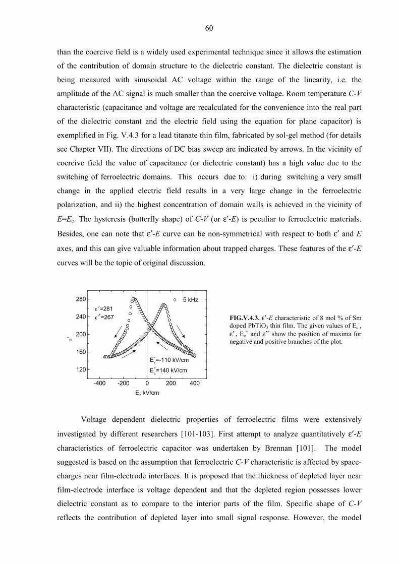
60
than the coercive field is a widely used experimental technique since it allows the estimation
of the contribution of domain structure to the dielectric constant. The dielectric constant is
being measured with sinusoidal AC voltage within the range of the linearity, i.e. the
amplitude of the AC signal is much smaller than the coercive voltage. Room temperature C-V
characteristic (capacitance and voltage are recalculated for the convenience into the real part
of the dielectric constant and the electric field using the equation for plane capacitor) is
exemplified in Fig. V.4.3 for a lead titanate thin film, fabricated by sol-gel method (for details
see Chapter VII). The directions of DC bias sweep are indicated by arrows. In the vicinity of
coercive field the value of capacitance (or dielectric constant) has a high value due to the
switching of ferroelectric domains. This occurs due to: i) during switching a very small
change in the applied electric field results in a very large change in the ferroelectric
polarization, and ii) the highest concentration of domain walls is achieved in the vicinity of
E=Ec. The hysteresis (butterfly shape) of C-V (or ε′-E) is peculiar to ferroelectric materials.
Besides, one can note that ε′-E curve can be non-symmetrical with respect to both ε′ and E
axes, and this can give valuable information about trapped charges. These features of the ε′-E
curves will be the topic of original discussion.
FIG.V.4.3. ε′-E characteristic of 8 mol % of Sm doped PbTiO3 thin film. The given values of Ec
-, ε′-, Ec
+ and ε′+ show the position of maxima for negative and positive branches of the plot.
Voltage dependent dielectric properties of ferroelectric films were extensively
investigated by different researchers [101-103]. First attempt to analyze quantitatively ε′-E
characteristics of ferroelectric capacitor was undertaken by Brennan [101]. The model
suggested is based on the assumption that ferroelectric C-V characteristic is affected by space-
charges near film-electrode interfaces. It is proposed that the thickness of depleted layer near
film-electrode interface is voltage dependent and that the depleted region possesses lower
dielectric constant as to compare to the interior parts of the film. Specific shape of C-V
reflects the contribution of depleted layer into small signal response. However, the model
-400 -200 0 200 400
120
160
200
240
280
ε'
E, kV/cm
5 kHz
E-c=-110 kV/cm
E+c=140 kV/cm
ε'-=281ε'+=267

61
needs to be extended to take into account asymmetrical nature of C-V characteristics due to
imprint and built-in field (will be discussed later), obtained for real metal-ferroelectric-metal
capacitors (Fig.V.4.3). Difference in bottom electrode-film and top electrode-film interfaces
due to different thermal histories is also not taken into account. Chai et al. [102] developed
domain-related model for C-V characteristics of the films. 1, 3 and 5 mol % of Nb doped PZT
50/50 thin films were investigated. Specimens were prepared on platinized silicon substrates
using sol-gel method. Asymmetries of C-V characteristics were attributed to correlation
between ferroelectric properties of the films and dopant-ion induced local-field variation
through the depth of the capacitors [102]. Vorotilov et al. [103] investigated sol-gel deposited
PZT thin films deposited on platinized silicon wafer. As in the case exemplified in Fig. V.4.3,
strong shift along field axis and non-symmetry of C-V curve with respect to capacitance axis
were observed. It was suggested that disturbed layer near bottom electrode may screen
effectively external bias field causing asymmetrical nature of C-V curves.
V.5. Ferroelectric properties.
Ferroelectric properties of the films are also known to be determined by method of
deposition, microstructure and choice of electrode material. The best ferroelectric properties
(high remnant polarization and low coercive field) were found for epitaxial films. Example of
FIG.V.5.1. Field-polarization hysteresis loop of epitaxial PZT thin film, deposited by pulsed laser ablation [73].
ferroelectric hysteresis loop of PZT film, deposited on MgO substrate by PLD is presented in
Fig. V.5.1 [73] where high remnant polarization can be seen. Polycrystalline films usually
show somewhat lower ferroelectric properties. Fig.I.1.3(a) exemplifies the hysteresis loop of
sol-gel fabricated film. Remnant polarization and coercive field were found to be 15 µC/cm2
and 58 kV/cm, respectively [10]. Influence of fabrication parameters on ferroelectric
properties of polycrystalline ferroelectric thin films has been investigated by many research
groups. Es-Souni et al. [80] discussed ferroelectric properties of Nb doped PZT thin films in

62
terms of microstructure and preferentially oriented state. Better results (higher value of
remnant polarization) were reported for (111) preferentially oriented samples. It must be
stressed here that correlation between microstructure and ferroelectric properties is still an
object of controversy. Lian and Sottos [67] compared (100) and (111) preferentially oriented
films. The former revealed noticeably higher remnant polarization. Whether the film is
randomly crystallized or preferentially oriented is determined by processing condition and
doping (will be discussed in more details in the following). It is also suggested that
ferroelectric properties strongly correlate with type of sol-gel route. Kwon et al. [38] prepared
PZT thin films using Acetate-, 2- methoxyethoxide-, and 2-ethilhexanoate-based precursor
FIG.V.5.2. Effect of sol-gel precursor on ferroelectric properties of PZT thin films [38].
solutions. Dependence of ferroelectric properties on sol-gel chemistry was revealed. Fig.V.5.2
exemplifies P-V characteristics, obtained for the films prepared from different precursor
solutions [38]. Well developed and saturated hysteresis loops were acquired for acetate- and
2-methoxyethoxide-based films (although, value of remnant polarization is noticeable smaller
than that found for epitaxial PZT film [73]). Poorly developed P-V curves were obtained for
the films deposited using 2-ethilhexanoate-based precursor.
Algueró et al. [104] discussed ferroelectric properties of lanthanum doped PbTiO3 thin
films deposited by sol-gel method on silicon substrates. Microstructure and phase content
were found to be dependent on excess PbO added to the sol to compensate lead volatility
during annealing. They suggest that ferroelectric properties of their specimens are chiefly
determined by the grain size of the films, which, they claim, is dependent of PbO excess, viz.
with increasing PbO excess from 10 to 20 mol %, the grain size decreases from approximately
1 µm to 100 nm.
Furthermore, doping by various impurities can affect ferroelectric hysteresis of the
films. Modification of ceramics by donor or acceptor elements to tune the properties for
specific application is widely used in industry (see ref. 8). The effects of doping on

63
ferroelectric properties of thin films are also reported for lead based perovskite thin films of
different compositions (see next paragraph for more details). As an example Fig.V.5.3
represents hysteresis loops obtained by Mah et al. [105] for La doped (Pb1-xLax)(Zr0.5Ti0.5)O3
films. Incorporation of La into the perovskite lattice caused the reduction of ferroelectric
characteristics (Pr and Ec). Similar trend (the reduction of ferroelectric characteristics with
increasing La content) was reported by Es-Souni et al. [106] and Kurchania and Milne [107]
for PLZT films derived by sol-gel technique. Dobal et al. [108] measured ferroelectric
hysteresis loops of Ce doped PLT films. It is reported that remnant and spontaneous
polarization are generally increases with Ce content. The same behaviour was observed by
Chang and Desu [72] and Matsuzaki and Funakubo [109] for La doped PZT and Nb doped PT
thin films, respectively. Teowee et al. [110] reported that remnant polarization of La doped
PZT 65/35 thin films shows a maximum in the vicinity of 4 mol % of La. In the other words,
ferroelectricity in thin films is far more complex than in bulk ceramics and is still an object of
intensive research.
FIG.V.5.3. Hysteresis loops of PLZT thin films modified with various amounts of La [105].
Finally, dependence of ferroelectric characteristics of polycrystalline films on the
nature of bottom electrode was investigated by many research groups. The use of conductive
oxide instead of metallic platinum or gold electrodes can cause some improvement in
ferroelectric properties and fatigue resistance of ferroelectric thin films. In particular,
fabrication and characterization of BaTiO3 and PZT thin films upon lanthanum nickel oxide
(LNO) electrode were reported [31, 111-114]. Fig. V.5.4 exemplifies ferroelectric hysteresis
loops of PZT thin films deposited on stainless steel (a), titanium (b) and nickel (c) substrates

64
FIG.V.5.4. Hysteresis loop of PZT thin films on (a) stainless steel, (b) titanium and (c) nickel substrates annealed at 600°C, measured at 180 kV/cm. Solid lines are for the PZT films fabricated incorporating LNO layers and dotted lines are for the PZT without LNO layers [111]. with and without lanthanum nickel oxide buffer layers [111]. The results unambiguously
demonstrate that good ferroelectric response can be achieved for the films deposited on LNO
buffer layer. Contrary, film deposited on bare metallic substrate revealed significant
degradation of ferroelectric properties due to chemical interaction of the films with the
substrate material.
V.6. Curie phase transition temperature.
Similar to bulk ceramics or crystals, the dependence of the dielectric constant of
ferroelectric thin films shows anomaly in the vicinity of Curie transition temperature.
However some specific features of the behaviour of ferroelectric films near ferroelectric-to-
paraelectric phase transition were reported. Fig. V.6.1 shows the temperature dependent
dielectric constant of Ba0.7Sr0.3TiO3 thin film in comparison to that of bulk ceramics of the
same composition (after Shaw et al. [115]). As can be seen, the ceramic specimen shows a
sharp peak in the vicinity of 300K, which is attributed to ferroelectric-to-paraelectric phase
transition, whereas the thin film demonstrates a very broad transition. Furthermore, a close
look at the figure reveals that the BST film undergoes ferroelectric-to-paraelectric phase
transition at remarkably lower temperature. Shaw et al. [115] explain the phenomenon from
the point of view of stress development during film fabrication. Moreover, as reported in

65
recent work of Chattopadhyay et al. [116] for epitaxial BaTiO3 thin film, Curie temperature
decreases smoothly with decreasing film thickness. Additionally, broadening of ε′(T)
characteristics was observed for thinner films. As in the former case, the results are treated in
terms of stress state development effect. In bulk barium titanate and strontium titanate
compressive stress dependent dielectric properties and Curie phase transition temperature
were systematically investigated by Samara [117]. It was observed that Curie temperature
decreases linearly with increasing pressure with the rate being in the range from -4.6 to -5.9
°C/kbar. Dausch and Haertling [118] claimed that lead lanthanum zirconate titanate thin films
undergo ferroelectric-to-paraelectric phase transition at higher temperatures compared to
ceramics of the same compositions. The results obtained were explained from the point of
view of stress development during cooling. Rossetti et al. [119] calculated possible shift of
Curie transition temperature in epitaxial lead titanate thin film. It was predicted that two-
dimensional compressive stress oriented orthogonal to the c-axis increases Curie temperature,
while hydrostatic (three-dimensional) compressive stress reduces Curie temperature.
FIG.V.6.1. Variation of the dielectric constant of Ba0.7Sr0.3TiO3 bulk ceramics and a film as a function of temperature [115].
The grain size is an additional parameter which determines deviation of Curie
temperature from crystal value. Okazaki and Nagata [120] investigated the dielectric
properties of PLZT ceramics of composition (Pb0.92La0.08)(Zr0.65Ti0.35)0.98O3. It was shown that
with the decreasing grain size from 4 µm to 1.5 µm, the Curie transition temperature increases
from approximately 120 to 140 °C. This effect was explained taking into account surface
layer of the grains. This layer possesses specific properties which differ from those of interior
part of grain. Following Okazaki and Nagata [120], in particles less than 5 µm in size, the
effects of the surface layer in which the ferroelectric polarization is locked-in by the space-

66
charge layer become increasingly important. If the locked-in ferroelectric polarization inside
each domain persists to temperature, far beyond the usual Curie point, the ferroelectric-
paraelectric transition temperature can be expected to increase with decreasing grain size,
because, when the grain size decreases, the surface area of the space-charge layer increases,
and both the space-charge field and the locked in ferroelectric polarization increase
simultaneously. This mechanism explains the grain-size dependence of the Curie point. On
the other hand, Curie transition temperature of ferroelectric thin films and nano-sized powders
shows completely opposite behaviour. Chattopadhyay et al. [121] studied Curie phase
transition in nanocrystalline PbTiO3 powder. They revealed a decrease in phase transition
temperature with decreasing particle size. The most pronounced effect was found for particles
size less than 100 nm. This behaviour was attributed to size induced structural distortion, viz.
lattice tetragonality decreases with decreasing particle size.
To recapitulate, shift of the Curie phase transition temperature of ferroelectric thin
films arises from the superposition of two effects, which must be taken into account. One is
stress development and another one is related to grain size. Contribution of these effects into
the measured value of Curie temperature depends on thin film microstructure, thermal
expansion properties of substrate and thin film and thermal history of the sample.
V.7. Doping effects.
In order to tune the properties of interest, the effect of doping is under investigation by
many research groups. In general, the term “doping” implies either that some ions, whose
chemical valence is different from those of the original ions in the lattice [pp. 133-140 in ref.
8], or some compounds with a chemical formula A+B5+O32- or A3+B3+O3
2+, are added during
materials processing. Depending on the type of additive one can distinguish between “soft”
and “hard” dopants (effect of isovalent elements doping is out of scope of the present work).
Ions for soft doping include La3+, Nd3+, and other rare earth, Sb3+, Bi3+, Th4+, Nb5+, Sb5+, W6+,
etc. The softening effect of soft doping is attributed to the creation of cation vacancies in the
perovskite lattice when the soft doping ions enter the lattice structure [6]. Soft doping
counteracts the natural p-type conductivity of the PZT and thus increases the electrical
resistivity of the material by at least 3 orders of magnitude. A-site vacancies introduction
enhances domain mobility under applied electric field and results in better ferroelectric and
piezoelectric properties [6]. Ceramics produced with these additives are characterized by
square hysteresis loop, low coercive fields, high remnant polarization, high dielectric

67
constant, maximum coupling factor, higher dielectric loss, high mechanical compliance, and
reduced aging. Hard doping ions in PZT include K+, Na+, which occupy A-sites and Fe3+,
Co2+, Mn2+, Mn3+, Ni2+, Mg2+, Al3+, Ga3+, In3+, Cr3+, and Sc3+, which occupy B-sites in the
perovskite structure. Hard doping is accompanied by oxygen vacancies which have only
limited solubility in the lattice. Domain reorientation is “hard” since oxygen vacancies serves
as the effective pinning centers. Hence, ceramics with acceptor-type additives are
characterized by poorly developed hysteresis loops, lower dielectric constant, low dielectric
losses, and low compliances. High mobility of the oxygen vacancies results in higher aging
rates. The most well known doping effect is perhaps La doping of PZT ceramics (PLZT)
which opened the way for the production of technologically important transparent ceramics
for electro-optical applications. After optical transparency of hot-pressed ferroelectric PLZT
ceramics was achieved in 1969 and PLZT compositional phase diagram established (1970)
(see Introduction) this group of material has been attracting attention. The first attempt to
fabricate PLZT thin films by sol-gel method was done by Budd et al. [25]. Ever since a large
number of reports on the effects of different doping elements appear every year. Despite that,
the systematic investigations of rare-earth elements doped ferroelectric materials, particularly
in the case of thin films, are still lacking. Investigations undertaken by Tan et al. [122],
Sharma et al. [123], Boyle et al., [124] and Park et al. [125] showed for ceramics and thin
films of different compositions that lanthanides smaller than La have the tendency to
substitute on B-site, leading to an acceptor-type behaviour (they substitute elements (Zr and
Ti) with higher valence). Boyle et al. [124] investigated lanthanide series doping effects in
PLnZT 4/30/70 thin films prepared by sol-gel method. It is shown that the elements from La
to Gd substitute A-site i.e. are donors, elements from Th to Ho are amphoteric i.e. can occupy
both A- and B-sites, and elements from Er to Lu substitute B-site, i.e. are acceptors and thus
substitute Zr and Ti in B-sites. Park et al. [125] investigated PLZT ceramic modified with 3
mol % of lanthanide elements. The same tendency towards B-site substitution with decreasing
ionic radius is concluded. Thus, atomic number of lanthanide element (hence, ionic radius)
was found to determine the substitution site. The conclusions about the distribution of doping
elements between A and B site are made considering the tolerance (or Goldschmidt) factor
(see paragraph I.1, equation (I.1.2) and ref’s 9 and 126). According to the rules of
Goldschmidt, the position of the dopant in the A or the B site can be determined if the host
ion and the substituted ion radii do not differ by more than 15 %.
A model for the calculation of the average size of A- and B-sites for the case of PZT
type solid solution can be found in the work of Gonnard and Troccaz [126]. Thereby with

68
FIG.V.7.1. Temperature dependent dielectric constant and dissipation factor (loss tangent) of PLZT ceramics, modified with lanthanide ions (from the original paper of Park et al.[125])
decreasing ionic radii of the lanthanide element the tendency to substitute B-site rather than
A-site is expected. Change in substitution type was found to strongly affect ferroelectric,
dielectric and structural properties of the material. Moreover, structural sensitive parameters,
such as Curie transition temperature correlate with radii of doping elements. The data, taken
from the original work of Park et al. [125] (Fig.V.7.1) illustrate how the paraelectric-to-
ferroelectric phase transition temperature can be changed in Ln elements doped PLZT
ceramics. Shannigrahi et al. [127] fabricated and explored Er doped PZT ceramics. La- and
Sm-modified PZT ceramics were investigated by Pramila et al. [128]. Some improvement of
ferroelectric properties and fatigue resistance in Ce doped PZT thin films have been reported
by Majumder et al. [129], who suggest that Ce can be distributed between A and B sites in 3+
and 4+ oxidation states, respectively. Structural and electrical properties of Gd and Ce doped
(Pb,La)TiO3 thin films have been investigated by Dobal et al. [108]. We note that Shannigrahi
et al. [127] treat Er as A-site donor, contrary to what is proposed by Boyle et al. [124] and
Park et al. [125]. Sharma et al. [123] also proposed rare-earth elements to be A-type donors.
They claim that along with the ionic radii, the electronic configuration of rare-earth elements
play an important role in the structural properties of perovskite-type materials. The

69
distribution of rare-earth elements between A and B sites seems also to depend on doping
element concentration [128 and references therein].
It must be mentioned that (as usually accepted in the literature) the term “dopant” is
used for atomic percentages less than 5%. Above this value, the compound is called
“modified”. Because the present work deals with doping levels from 2 to 8 mol % of rare-
earth ions, the terms will not be discerned for simplicity.
V.8. Leakage currents.
In view of leakage currents being known as one of the most important factors limiting
the application of ferroelectric thin films in memory devices, this phenomena has been
investigated extensively for barium strontium titanate (BST) [91,92,130], SrTiO3 [131]
Bi4Ti3O12 [132] and lead-based titanates [48,96,133-138]. The analysis of temperature- and
voltage-dependent leakage currents in polycrystalline thin films is one of the most
complicated issues, since different conduction mechanisms may take place in the same
temperature and voltage ranges. Review of basic conduction processes in dielectric films can
be found in textbooks (see, for example Scott [15] and Sze [139]).
FIG.V.8.1. Energy-band diagram of a contact between a metal surface and a vacuum. The metal work function is qφm. The effective work function (or barrier) is lowered when an electric field is applied to the surface. The lowering is due to the combined effects of the field and the image force (p.250 in ref. 139).
Following Scott [15], ferroelectric film capacitors on metal electrodes consists of very
complex structures in which electrons, holes, and ions all contribute to conduction, and where
a variety of mechanisms – including surface-limited processes such as thermionic Schottky
z
z
z

70
currents and quantum mechanical Fowler-Nordheim currents, as well as bulk-limited
processes such as Poole-Frenkel and Space-Charge-Limited Currents (SCLC) can all play an
important role. Typically these processes are all present at the same time, and unfortunately
they are not additive; rather, they result in non-linear integral equations for total leakage
current J(V).
The Schottky conduction mechanism is based on the image-force-induced lowering of
the potential energy for charge carrier emission when an electric field is applied across metal-
semiconductor interface. When an electron is at the distance z from the metal, a positive
charge will be induced on the metal surface. The force of attraction between the electron and
induced positive charge is equivalent to the force that would exist between the electron and an
equal positive charge located at –z. This positive charge is referred to as the image charge.
The attractive force, called the image force, is given by the Coulomb relation (p. 250 in
ref.139):
2 2
2 20 04 (2 ) 16
q qGz zπ ε πε
− −= = (V.8.1)
where q is the charge of the electron and ε0 is the permittivity of free space. The work done by
an electron in the course of its transfer from infinity to the point z is given by
2
0
( )16
z qA z Gdzzπε∞
= =∫ (V.8.2)
when an external field E is applied, the total potential energy PE as a function of distance is
given by the sum
2
0
( )16
qPE z qEzzπε
= + (V.8.3)
at the equilibrium position
2
20
( ) 016
dPE z q qEdz zπε
= − + = (V.8.4)
The Schottky barrier lowering (also referred to as image force lowering) ∆φB and the location
of the lowering, zm are given by
016m
qzEπε
= (V.8.5)
and

71
0
24B mqE Ezφπε
∆ = = (V.8.6)
Corresponding energy-band diagram is shown on Fig.V.8.1 [139]. The equations can also be
applied to metal-semiconductor systems. However, the field should be replaced by the
maximum field at the interface, and the free-space permittivity ε0 should be replaced by an
appropriate permittivity ε, characterizing the semiconductor medium, that is,
4BqEφπε
∆ = (V.8.7)
The current density is expressed as:
( / 4 )2* expq qEBJ A T
k TB
φ πε− −=
(V.8.8)
if Schottky-type emission is the process, determining charge transport in dielectric film. A* is
so-called effective Richardson coefficient.
The Poole-Frenkel emission (p. 402 in ref. 139) occurs due to field-enhanced thermal
excitation of trapped electrons into conduction band. Current density for the case of Poole-
Frenkel emission is given by the equation:
( / )
expq qEBJ E
k TB
φ πε− −≈
(V.8.9)
For trap states with coulomb potentials, the expression is virtually identical to that of the
Schottky emission. The barrier height, however, is the depth of the trap potential well, and the
quantity /q πε is larger than in the case of Schottky emission (V.8.8) by a factor of 2, since
the barrier lowering is twice as large due to the immobility of the positive charge.
The space-charge-limited current (SCLC) results from a carrier injected into the
insulator, where no compensating charge is present. The current for the unipolar trap-free case
is proportional to the square of the applied voltage. In SCLC regime current varies with
thickness of insulating film not ohmically (1/d), but as 1/d3. This
2
3
VJ Bd
= (V.8.10)
dependence is known as the Mott-Gurney law (p.86 in ref.15). B is proportional to dielectric
constant of the material and mobility of electrons µe. In more general case current density is
expressed as [96]:
n
m
VJ Bd
= (V.8.11)

72
where n and m are voltage and thickness exponents, respectively.
As already mentioned, leakage current phenomena are being extensively investigated
in different systems of ferroelectric materials. BST, PZT, PT, PLZT and BTO (bismuth
titanium oxide) are among them. Paek et al. [91] showed that leakage current through BST
thin films decreases with increasing film thickness. This effect was attributed to change in
microstructure as function of film thickness. In fact, SEM and HRTEM observations
confirmed that grain size in sputtered BST films increases with film thickness. Grain
boundaries were treated as the leakage current paths. From this point of view it is expected to
observe increased contribution of grain boundaries into conduction processes for thinner
films. However, voltage and temperature dependences of leakage current were not presented.
More detailed analysis of leakage currents in BST thin films were reported by Hwang et al.
[92] who discussed the influence of deposition techniques on conduction behaviour. It was
claimed that BST and Pt junction form so-called blocking contact with potential barrier
strongly dependent on deposition method. While the barrier height for sputtered film was
found to be 1.6-1.7 eV, OMCVD deposited film was characterized by a value of 1.2 eV.
Different interfacial properties of the films were claimed to be the reason for these results. It
was also suggested that at low temperature tunnelling processes are responsible for charge
transport. At high temperature Schottky type conductivity is dominant. Change of operating
mechanism occurs at temperatures of about 120°C.
Nagaraj et al. [130] investigated leakage current in all-perovskite LSCO (lanthanum
strontium cobalt oxide)/BST/LSCO system. From J-E measurements it was inferred that bulk-
limited Poole-Frenkel mechanism is predominant in the investigated system. The same
conclusion was drawn by Al-Shareef and Dimos [137] for conduction processes in lead
titanate thin films.
The role of SCLC mechanism in PZT thin film has been discussed by Shin et al. [96].
It was shown that this mechanism is dominant at high values of applied bias (E>400 kV/cm)
whereas at lower field, conduction processes are being operated by Schottky emission. Space-
charge-influenced-injection model has been advanced by Stolichnov and Tagantsev [134].
They analyzed voltage and time dependent leakage currents in PZT thin films fabricated on
platinized Si substrates by sol-gel, OMCVD and sputtering techniques. Following the
proposed model, the leakage current is determined by carriers injection through the electrode
(the carriers injected are holes). Specifically, the current is limited by the built-in charge in
near-electrode area which has the same sign as the injected carriers due to upward band
bending near the electrodes.

73
Cho and Jeon [135] showed that not only the leakage current magnitude but also the
type of operating mechanism is sensitive to processing conditions. The fitting of the J-E
curves obtained for sol-gel processed PZT films to different (interface and bulk limited)
conduction processes revealed Schottky type emission for the specimen annealed in N2
atmosphere and mixed Schottky and SCLC conductivity for the specimen annealed in O2
atmosphere.
In another report Stolichnov et al. [136] discussed the role of electrode material in the
degradation of the leakage properties of PLZT thin films (hybrid Pt/SRO (strontium
ruthenium oxide) structure was utilized as the top electrode). The authors supposed that
diffusion from the electrode into the thin film material can cause leakage current increase
through the capacitor. They concluded that electrode material is one of the critical parameters
determining the performance of ferroelectric thin film devices.
Finally, the effects of donor doping on the leakage currents in PZT thin films were
reported by Kim et al. [138]. They obtained lower leakage current density in Nb and La doped
films as compared to non-doped specimens, which is expectable bearing in mind p-type
conductivity of PZT.
It can be concluded that the leakage currents in ferroelectric thin film capacitors are
affected by various factors such as fabrication conditions, microstructure, electrode material
and doping. Appropriate choice of deposition parameters, substrate and doping can suppress
conductivity and thereby improve the quality of the device. From fundamental point of view,
the mechanisms of conductivity are still subject of controversy, and the phenomenon of
leakage current in ferroelectric thin films is not well understood. Systematic investigations
including thickness effects, voltage and temperature dependences as well as type of electrode
material are therefore needed for a thorough understanding of the conduction mechanisms in
ferroelectric thin films.
V.9. Pyroelectric and piezoelectric properties of ferroelectric thin films.
Pyroelectric and piezoelectric properties of lead-based perovskite thin films prepared
by different methods are considered for applications in integrated IR detectors and imaging
devices and MEMS by many research groups [43, 140-144]. The possibility to fabricate high
quality thin films with pyroelectric coefficients comparable to those known for bulk ceramics
has been demonstrated [140,141]. It was shown that composition of thin film is critical for
pyroelectric properties. Tseng et al. [142] reported on preparation and characterization of lead

74
titanate thin films substituted with various amounts of La by pulsed laser deposition. Films
modified with 10 mol % of La (PLT10) revealed a higher pyroelectric coefficient compared to
that of 5 mol % modified film (PLT5). This result was explained in terms of La induced
decrease of the Curie transition temperature (it is known that the pyroelectric coefficient of
ferroelectric materials reach maximum in the vicinity of the phase transition temperature).
Similar effects of La doping on pyroelectric properties was reported by Kamada et al. [143]
for RF-magnetron sputtered PbTiO3 thin films. Furthermore, it was discovered [44,140,141]
that while non-poled ferroelectric ceramics do not show any pyroelectric activity, as-grown
thin films reveal measurable pyroelectric response. This effect is attributed to self-polarization
developed in films during cooling through the Curie transition temperature. This effect is
reported to be very stable and comparable to subsequent room temperature poling [144].
Compared to bulk ceramics, the piezoelectric properties of lead based thin film were
studied to a lesser extent. In general, the piezoelectric response of ferroelectrics is determined
by the contribution of domain structure which, in turn, depends on grain size. Ferroelectric
thin films with grain sizes below 1 µm demonstrate lower piezoelectric coefficients compared
to bulk ceramics [145]. Film thickness and texture dependent piezoelectric properties are
another important feature of ferroelectric thin films. Lian and Sottos [67] investigated the
piezoelectric properties of PZT thin films with emphasis on thickness and preferentially
oriented state effects. The piezoelectric coefficient was found to decrease with the film
thickness. This result was attributed to residual stress in the films which relaxes as thickness
of the films increases. On the other hand, films grown with (100) preferred orientation were
found to have a higher piezoelectric constant than that of (111) preferentially oriented films.
Doping effects on the piezoelectric properties were mainly addressed in bulk ceramics [6,8].
The piezoelectric properties of thin films arise from the superposition of many factors such as
doping, thickness, stress state, grain size, nature of electrodes, preferred orientation of grains
in polycrystalline films, self-polarization states and presence of electrode-film interfacial
layers and are, therefore, more complex than in bulk materials.

75
VI. Aims of this work
Analysis of the literature available revealed that La is the most explored doping
element in lead-based ferroelectric ceramics and thin films. Effects of doping by other
elements of lanthanide series were mainly investigated in PZT and PLZT bulk ceramics and
have not been adequately understood in the case of thin films. Moreover, to our knowledge,
systematic efforts to investigate the dependence of structural, optical and electro-physical
properties of lead titanate thin films on rare earth elements type and concentration were not
undertaken. In view of increasing importance of application of ferroelectric thin films in up-
to-date device technology, it is considered to be necessary to trace the structural and electro-
physical properties of the films with regard to the nature and concentration of doping ions. It
is believed that it is important to demonstrate the possibility of the most critical properties
from the point of view of thin films application (optical, dielectric, ferroelectric properties and
leakage currents) to be tailored by appropriate doping. It is also believed that detailed analysis
of dielectric, ferroelectric and leakage properties of the films can cast light onto the
substitution type and distribution of lanthanide elements between A- and B-sites of perovskite
lattice with respect to their ionic radii. For this purpose, conventional sol-gel method is
adopted to process films because it provides versatile and cost-effective processing route with
controlled stoichiometry and microstructure. (111)Pt/Ti/SiO2/Si and
LaNiO3/(111)Pt/Ti/SiO2/Si heterostructures are taken as the substrates. Commercially
available (111)Pt/Ti/SiO2/Si substrates are used in the majority of the cases for polycrystalline
thin films deposition. Considering the effect of substrate on the structural and electrophysical
properties of the films, the same substrates is utilized in the present work purposely to
compare correctly the results obtained with those published by other research groups.
Utilization of conducting oxides as an electrode material instead of traditional metallic
(platinum or gold) was discussed in literature [31, 111-114]. Although the improvement of
thin films performance was reported, correlation between structural, dielectric and
ferroelectric properties and kind of substrate have not been investigated systematically.
It was also shown that such effects as imprint and thickness dependent properties
found especially for the ferroelectric thin films significantly limit the area of possible

76
application. Understanding the nature of these effects will contribute to the improvement of
the material performance.
In this work, the results obtained on microstructure development and Ln-doping
effects on properties of lead titanate thin films are summarized. Attention is also paid to
effects due to bottom electrode material and film thickness. The results are discussed taking
into account substitution site preference, film texture, lattice parameters modification and
stress states. Owing to the importance of ferroelectric thin films in device development, the
pyroelectric and piezoelectric properties of selected films are also investigated. The attempt to
tailor pyroelectric and piezoelectric response from the thin film detector via the doping with
lanthanide elements is done.

77
VII. Preparation and characterization of lanthanide ions doped PbTiO3 thin films: experimental details
In the present chapter the detailed procedure of sol-gel processing used for specimen
preparation is described. The main efforts were directed towards optimization of thermal
conditions and precursor solution properties in order to obtain high quality, crack-free
samples with controlled microstructure and thickness, crucial for the comparative
characterization to follow. The experimental techniques involved in the characterization of the
structural and electrophysical properties are also described in the corresponding sections.
VII.1. Sol-gel fabrication of pure and rare-earth substituted PbTiO3 thin films
and optimisation of deposition parameters.
Acetic acid, acetylacetone and 2-methoxyethanol modified sol-gel method was utilized
to fabricate pure and lanthanide (Ln) elements doped lead titanate thin films. The flow chart
diagram shown in Fig.VII.1.1 illustrates the process of precursor solutions preparation. Lead
acetate, tetraisopropyl orthotitanate, acetic acid, acetylacetone and 2-methoxyethanol were
provided by Fluka Chemical, Inc., Germany. Ce, Sm, Dy, Er and Yb acetates were purchased
from Strem Chemicals, Inc., U.S.A. The stoichiometry of doped specimen was Pb(1-x)LnxTiO3,
where x = 0.02, 0.05 and 0.08. I.e. 2, 5 and 8 mol % of lanthanide ions were designated to
substitute lead on A-sites. Firstly lead and Ln acetates were dissolved in acetic acid and
refluxed for 3 hours at 110°C to evaporate associated water. 3 mol of acetic acid were taken to
dissolve 1 mol of lead and Ln acetates. Tetraisopropil orthotitanate was stabilized with
acetylacetone in a ratio of 1:2 mol. Both parts were then mixed together at room temperature
and diluted with 2-methoxyethanol to reach the final concentration of 0.5 mol/l. Regardless of
the type of dopant and doping level, yellow, transparent sols were obtained. The solutions
were filtered through 0.2 µm syringe filter just prior to film deposition. The films were
formed by multiple spin-coating depositions onto different substrates with 3000 rpm for 30 s
using Chemat Technology, Inc. (USA) KW-4A photoresist spin-coater. Each coating was
dried on a hot plate at 340°C for 5-10 min followed by annealing at temperatures between 550
and 700°C.

78
FIG.VII.1.1. Flow chart diagram of PLnT precursor solution preparation.
It is known that lead is the most volatile element in PZT based solid solutions [146].
Purposely to compensate lead loss during high temperature annealing of the specimens lead
excess is being added at the stage of sol preparation. At the same time, excessive Pb can lead
to the formation of liquid phase that in turn affects microstructure of the specimens. In order
to trace the effect of lead excess on the morphology of the films and optimize their
microstructure, 0, 10 and 20 mol % of Pb excess were added to non-doped lead titanate
precursor. As shown before [76], fabrication of pure lead titanate films is more difficult in
comparison to lanthanide elements doped samples due to strong cracking effects caused
probably by the high tetragonal distortion and stress development during cooling through the
Curie temperature. Similar deposition parameters (temperature and time of annealing, solution
concentration etc.) for pure and doped lead titanate films appear therefore difficult to maintain
[76]. At the same time, the electrophysical properties of ferroelectric films are very sensitive
to deposition parameters. In order to allow a meaningful discussion of the effects of doping
elements on the film properties to be made, the processing parameters were explored and
optimised first on pure lead-titanate for the purpose to obtain crack free films. The optimized
processing conditions were then adopted for doped and non-doped films. The processing
parameters explored were: annealing conditions, lead excess and sol concentration.
Pb acetate+Ln acetate+acetic acid;
stirring with distillation at110°C for 3 hours.
Tetraisopropyl orthotitanate+ acetylacetone;stirring at room
temperature for 10 min.
Dilute with2-methoxyethanol, filtering
through 0,2 µm filter.
Stable stock solution

79
Fig.VII.1.2 shows back scattered electron (BSE) SEM micrograph of lead titanate thin
films prepared from the sol of calculated stoichiometry Pb1.2TiO3 and consisting of 7 coatings.
The first layer was pre-annealed at 550°C for 10 min in order to reduce the energy of
crystallization of next layers. Then, three coatings were performed followed by pre-annealing
at 550°C for 10 min. Finally, additional three coatings were deposited and the specimen was
subsequently annealed in the furnace at 600°C for 10 min in air. As can be seen from the
surface morphology illustrated in Fig. VII.1.2, the deposition conditions described above lead
to rather coarse and non-uniform microstructure interspersed with cracks, but free from
visible second phase inclusions. The film thickness determined by means of SEM cross-
section specimen is about 650 nm. Under these conditions, crystallization was accompanied
with crack formation which is unacceptable for a proper characterization of the film
properties.
FIG.VII.1.2. BSE SEM top-view of lead titanate thin film, consisting of 7 layers of solution with the stoichiometry Pb1.2TiO3 and concentration 0.5 mol/l, annealed at 600°C for 10 min. Cracks appeared due to the development of stress during film crystallization are indicated by arrows.
Fig.VII.1.3 shows lead titanate processed from a sol containing no lead excess. The
film consisted of 3 layers, and annealed at 600°C for 10 (a), 20 (b) and 30 (c) min. The
reduction of the amount of deposited layers and the use of a stoichiometric sol composition
(with no lead oxide excess) has allowed to obtain crack-free films. On the other hand, it seems
that, regardless of annealing time, complete crystallization of the perovskite phase was not
achieved, and some fraction of a lead depleted phase, probably pyrochlore (lead depleted
areas are seen in the BSE micrograph as dark contrast areas because of atomic number
contratst) still exist.
In order to avoid lead depletion and to improve crystallization of the films, a Pb-
excess of 10 mol % was adopted, and a temperature of 700°C was chosen keeping the sol
concentration at 0.5 mol/l. Fig. VII.1.4 shows the microstructure obtained. One can see that
the film has been damaged by peeling probably due to high stress.

80
FIG.VII.1.3. BSE SEM micrographs of lead titanate thin films, processed from a stoichiometric sol and concentration of 0.5 mol/l. The films consisted of 3 layers with final annealing at 600°C for 10 (a), 20 (b) and 30 (c) min. Dark areas are Pb-depleted second phase particles, probably pyrochlore (indicated by arrows).
FIG.VII.1.4. Lead titanate thin film, prepared from the sol with 10 mol % Pb excess and the concentration 0.5 mol/l .The film consisted of 3 layers. Film was annealed at 700°C for 5 min.
Pb-depleted areas

81
FIG.VII.1.5. BSE SEM micrograph of PbTiO3 thin film deposited by sol-gel method upon (111)Pt/Ti/SiO2/Si commercial substrate. Film is fabricated from the sol containing 10 mol % of Pb excess and concentration 0.4 mol/l and consists of four coatings. Film was annealed at 700°C for 5 min.
The next step in the deposition optimization consisted in reducing the concentration of
the sol which leads to thinner individual layer. Considering the results of microstructural
characterisation presented above, it was inferred that the reduction of the sol concentration
can diminish the risk of cracking or peeling. Therefore, the sols were diluted with 2-
methoxyethanol to give a final concentration of 0.4 mol/l. The crystallization temperature was
kept at 700°C and the number of layers at four. It appeared that 5 min annealing time was
sufficient for well crystallized, fine grained films (Fig.VII.1.5). The same conditions were
then utilized to fabricate Ce, Sm, Dy, Er and Yb doped specimens. As mentioned above,
doping levels were set to 2, 5 and 8 mol %. However, a sol with 8 mol % Ce could not be
successfully prepared because of the low solubility limit of Ce-acetate in 2-methoxyethanol.
Doping with Yb led to high conductivity of the film for doping levels higher than 2 mol %.
These films were therefore omitted from further electrical characterization. The thickness of
the films was determined by means of ellipsometry (see corresponding sections for
experimental details). The microstructures of substituted films are very similar to that of non-
doped lead titanate. Fig’sVII.1.6(a-g) exemplify the AFM micrograph obtained in non-contact
mode for pure and doped with 2, 5 and 8 mol % of Sm and Er films. Mean grain size and root
mean square (RMS) roughness of the corresponding specimens are listed in Table VII.1.1.∗
For pyroelectric and especially piezoelectric properties characterization, thicker films are
preferable since it can increase signal-to-noise ratio and improve the quality of the data. 950
nm thick PST5 and PET5 thin films were fabricated on commercial (111)Pt/Ti/SiO2/Si
substrates. 12 layers in total were deposited under the following conditions. Each layer was
dried on a hot plate at 340°C for 5 min and pyrolized at 550°C for 5 min. Intermittent
annealing in a preheated furnace at 700 °C had to be used in order to avoid cracking.
∗ Grains diameter and RMS roughness were calculated using the scanning probe imaging processor (SPIP, version 2.3, Image Metrology) software.

82
FIG.VII.1.6. AFM micrographs of pure and Sm and Er doped films: PbTiO3, Pt electrode (a); PbTiO3+2 mol % Er, Pt electrode (b); PbTiO3+5 mol % Er, Pt electrode (c); PbTiO3+8 mol % Er, Pt electrode (d); PbTiO3+2 mol % Sm, Pt electrode (e); PbTiO3+5 mol % Sm, Pt electrode (f); PbTiO3+8 mol % Er, Pt electrode (g); PbTiO3+5 mol % Er, LNO/Pt electrode (h).

83
Table VII.1.1. Mean grain diameter and RMS surface roughness obtained from AFM investigations of pure and doped films (corresponding micrographs are shown in Fig’s VII.1.6 (a-g).
Mean grain diameter, nm Surface roughness (RMS), nm Doping level Sm Er Sm Er 0 143 7.7 2 114 107 4.73 4.32 5 100 102 2.06 4.85 8 98.7 141 3.08 8.44
To investigate thickness and the electrode material effects on the dielectric and
leakage current properties (see corresponding chapters), a set of specimens doped with 5 mol
% of Er was prepared on platinum and lanthanum nickel oxide (LNO). The films consisting of
three, four and six coatings were prepared under the conditions described above. Sol-gel was
utilized to produce the LNO buffer layer onto commercial (111)Pt/Ti/SiO2/Si substrates.
Lanthanum nitrate hexahydrate and nickel acetate were dissolved in 2-methoxyethanol in ratio
1:20 mol and refluxed with back-flashing at 135°C for 30 min. 2 layers were spin-coated,
dried on a plate at 340°C for 5 min before final annealing at 700°C for 10 min. A film
thickness of 67 nm was determined by means of ellipsometry. A AFM micrograph of 5 mol %
of Er doped film is shown in Fig.VII.1.6(h). RMS roughness and average grain diameter were
calculated for this specimen as 5.24 nm and 108 nm, respectively. Pure and doped lead
titanate films, involved in the present study are listed in Table VII.1.2.
Table VII.1.2. List of the lead titanate films investigated. The film thickness was obtained from ellipsometric measurements.
Film thickness Substrate Dopant Doping level,
mol % (111)Pt/Ti/SiO2/Si LNO/Pt/Ti/SiO2/Si
Sample designation
none - 267 - PT Ce 2 245 - PCT2
5 280 - PCT5 Sm 2 245 - PST2
5 308 950 - PST5 8 235 - PST8
Dy 2 224 - PDT2 5 208 - PDT5 8 264 - PDT8
Er 2 203 - PET2 5 200 285 375 950 195 260 390 PET5 8 212 - PET8
Yb 2 238 - PYT2

84
For electrical measurements, round Pt top electrodes with a diameter of 0.6 mm were
sputtered through a shadow mask. Post top electrode deposition annealing was conducted on a
plate at 400°C for 10-15 min. The contact to the bottom electrode was produced by scratching
a corner of the specimen and subsequent deposition of silver paste. For pyroelectric and
piezoelectric measurements (case of 12-layer films) Pt top electrodes of the configuration
shown in Fig. VII.1.7 were sputtered through a shadow mask, and annealed as described
above. In the interferometric measurements of the piezoelectric properties, the adjacent
(small) contact was used to apply the driving AC voltage whereas central (large) contact was
exposed to the laser. In the pyroelectric characterization of the films, opposite extra-contacts
were used to measure the temperature dependent resistance of the contact group (see below).
This specific configuration of the top electrode was developed since the existent experimental
set-ups did not allow getting the reliable contacts utilizing the conventional round electrodes.
FIG.VII.1.7. Scheme of the sputtered Pt top electrode utilized for pyroelectric and piezoelectric measurements. Central contact (diameter 1.5 mm) is connected via the strips (1x0.5 mm) with four extra contacts (diameter 1 mm).
VI.2. Experimental details on structural and electrophysical properties
characterization.
A. X-ray diffraction (XRD)
Phase characterization included Θ-2Θ and grazing incidence (GI) X-ray diffractometry
(Seifert 3000 PTS powder diffractometer equipped with four-cycle goniometer, CuKα
monochromated radiation, λ=1.5418 Å, grazing angle 2°). Θ-2Θ scans were measured in 2Θ
angle range from 20° to 50° with a step of 0.04° and a duration 20 s/step. For grazing
incidence experiment step width and duration were held at 0.05° and 10 s/step, respectively.
In-plane alignment was monitored by (100) pole figures, which were measured in Schulz
reflection geometry by scanning the tilt angle of the goniometer, Chi, in the range from 0° to
65° and azimuthal angle, Phi, from 0° to 360°, using a 2.5° step for both. No correction for
defocusing and absorption were introduced since, for the thickness of the film studied, both

85
effects compensate each other in the range of Chi used [52]. Fibre texture (FT) plots were
obtained by scanning χ angle with a step of 0.5°.
B. Raman spectroscopy
The Raman spectra were obtained at room temperature in back-scattered geometry
using a Dilor spectrometer supplied with micro-Raman set-up. 514 nm, 488 nm and 458 nm
lines from Ar-laser and 633 nm line from HeNe-laser were used. The collection time was
varied in the range from 5s to 100 s to optimize signal-to noise ratio and minimize the
contribution from the intense line of Rayleigh scattering.
C. X-ray photoelectron spectroscopy (XPS)
Additionally, oxidation state of Ce in Ce-substituted lead titanate thin films was
investigated by means of X-ray photoelectron spectroscopy using Al Kα monochromator
(Omicron Full Lab System). The measurements were performed on as-deposited films and
after Ar ion cleaning at 1 keV and 70 nA for 2 min.
D. Scanning electron microscopy (SEM)
The microstructures of the specimens were observed by means of scanning electron
microscopy (Philips XL 30). The best resolution was achieved by using the back scattered
electrons (BSE) imaging mode. SEM was mainly involved in specimen characterization
during optimisation of film deposition parameters (see paragraph VII.1).
E. Atomic force microscopy (AFM)
Additionally to SEM, AFM technique (Surface Imaging Systems) was used for
monitoring the microstructure of the films. Grains diameter and RMS roughness were
calculated using the scanning probe imaging processor (SPIP, version 2.3, Image Metrology)
software (see paragraph VII.1).
F. Ellipsometry
The thickness and optical properties (refractive index and extinction coefficient) of the
films prepared were measured by means of ellipsometry. Considering the data obtained at
λ=632.8 nm (HeNe-laser) for various incidence angle from 30° to 85° and four points of the
sample surface, an over determined system was achieved, which allowed for cross-checking,
increased resolution and testing the employed model. As a measure of the resolution, the

86
change in the thickness due to change in n by 1% is noted. The algorithm of the complex
refractive index calculation and optimisation was realized with MathCAD software [147,148].
The ellipsometric thickness of prepared thin films was found to be in the range from 200 to
300 nm (see Table VII.1.2). The refractive indices of the specimens were obtained from
ellipsometrically determined Ψ and ∆ utilizing equations (IV.6.1-IV.6.7). The film thickness
was then found as the result of parameters fitting to the film-substrate model (Fig.IV.6.3).
G. Ferroelectric hysteresis measurements
The ferroelectric hysteresis loops of the films were measured using Radiant
Technologies, Inc. RT6000S ferroelectric testing systems operated in a virtual ground mode
(VGM). The principles of this mode are described in paragraph IV.7. In our experiments, the
signal was applied to the bottom electrode of the ferroelectric capacitor structure. The
amplitude of the driving signal and pulse time were from 0.5 to 19 V and from 0.13 to 0.2 ms,
respectively.
H. Impedance and leakage current measurements
The dielectric properties (dielectric constant, loss tangent) of the ferroelectric films
can be characterized by the bridge methods depicted in Fig.IV.8.1. The leakage current
characteristics of the specimens are usually measured with high precision electrometers.
FIG.VII.2.1. Scheme of the set-up for characterization of dielectric and leakage properties of the films.
In the present work Agilent 4192A LRC meter (or impedance analyser) was utilized for
dielectric testing. The leakage current properties were investigated using Keithley 6517A
electrometer. Fig.VII.2.1 shows schematically the set-up utilized in this work for dielectric
LRC bridgeor electrometer
Heating stage
Sample
Operation anddata acquisition
to digital thermometer
Tem
pera
ture
sens
or
To th
eto
pel
ectro
de
To th
ebo
ttom
elec
trode
GPIB bus

87
and leakage properties characterization. The Curie temperatures, dielectric constants and loss
tangents of the films were investigated using an appropriate set-up including a heating stage
and Agilent 4192 A LRC meter. For measurements at elevated temperatures, the set-up
contains heating stage which allowed temperature controlling within an accuracy of 0.2-0.5
°C. Commercial GMH3230 (Greisinger Electronic, Germany) digital thermometer interfaced
with personal computer was utilized for sample surface temperature control. In the case of
impedance measurements, in order to exclude contribution from resistance and inductance of
wires and contact group (particularly at high frequency), measurement through overall
frequency range allowed by the device (from 5 Hz to 13 MHz) was conducted in a short-cut
regime. The data obtained were then subtracted from the experimental results.
I. Pyroelectric measurements
Pyrodynamic and bolometric measurements were performed using a self-made
experimental set-up including a computer controlled lock-in amplifier (Ametek 7225),
function generator (Agilent 33120 A), current source and voltmeter (Keithley 2420). The
thermal excitation is done sinusoidally with a Peltier element. Surface temperature
measurements are performed using the front electrode as a bolometer, Fig. VII.2.2. The lock-
in amplifier is employed to monitor the bolometric voltage variation. The Pt electrode is
contacted with two needles and the current and voltage is supplied and measured separately
(4-wire sense). For a constant current of 3 mA the measured voltage was found to be around
1.5 V. For the calibration of the Pt electrode as a bolometer, the Peltier element is modulated
at a frequency of 5 mHz and the temperature is monitored with a thermocouple element. The
amplitude of the temperature variation was about 1.4 °C and the resulting voltage amplitude
was around 2.2 mV. An evaluation method using the two first-order Fourier coefficients of
the temperature and voltage signals is applied to determine the amplitudes. From the
amplitudes the calibration coefficient can be calculated. The bolometric calibration was done
twice and the coefficients values of 0.6131 and 0.6162 °C/mV obtained were close to each
other. The dependence of surface temperature of the modulation frequency of thermal
excitation is computed from the measured bolometric voltage amplitude and the above-
mentioned coefficient. For pyroelectric coefficient measurements the temperature was
modulated in the frequency range from 30 mHz to 200 mHz and the pyroelectric coefficient
was obtained from measuring the resulting pyroelectric current as a consequence of
temperature changes in the ferroelectric material [45]. For sinusoidal temperature modulation

88
the pyroelectric coefficient of a ferroelectric film can be calculated from the pyroelectric
current:
pipTSω
∆=
∆ (VII.2.1)
It is assumed that the temperature variation is homogeneous in the film and hence equal to
measured surface temperature.
FiG.VII.2.2. Experimental set-up for bolometric and pyrodynamic measurements.
FIG.VII.2.3. Experimental set-up for piezoelectric measurements.
Peltier element
Current source
Voltage meter
Temperature sensor
to digital termometerSample
Top electrode
Lock-in amplifier
Function generator
G P
I Bbu
s
Film
Top electrode
Lock-in amplifier
Function generator
G P
I Bbu
s
Bottom electrode
Inte
rfer
omet
erhe
ad
Laser beam
Interferometer controller

89
J. Piezoelectric coefficients determination.
Interferometric technique was utilized to investigate the piezoelectric response from
selected specimens. Principles of Doppler heterodyne interferometer are described in
paragraph IV.11. The experimental set-up includes Polytec OFV 353 sensor head (laser
source and optical system), interferometer controller (Polytec OFV 3001), lock-in amplifier
and function generator. The set-up is schematically represented in Fig.VII.2.3. The laser beam
is focused on the front electrode of interest. An AC signal of various amplitudes and a
frequency of 1 kHz is applied using a computer controlled function generator to
corresponding pad to excite surface vibration (due to converse piezoelectric effect). The
output signal (surface velocity) from the interferometer controller is measured with the
computer operated lock-in amplifier and used for the calculation of surface displacement.
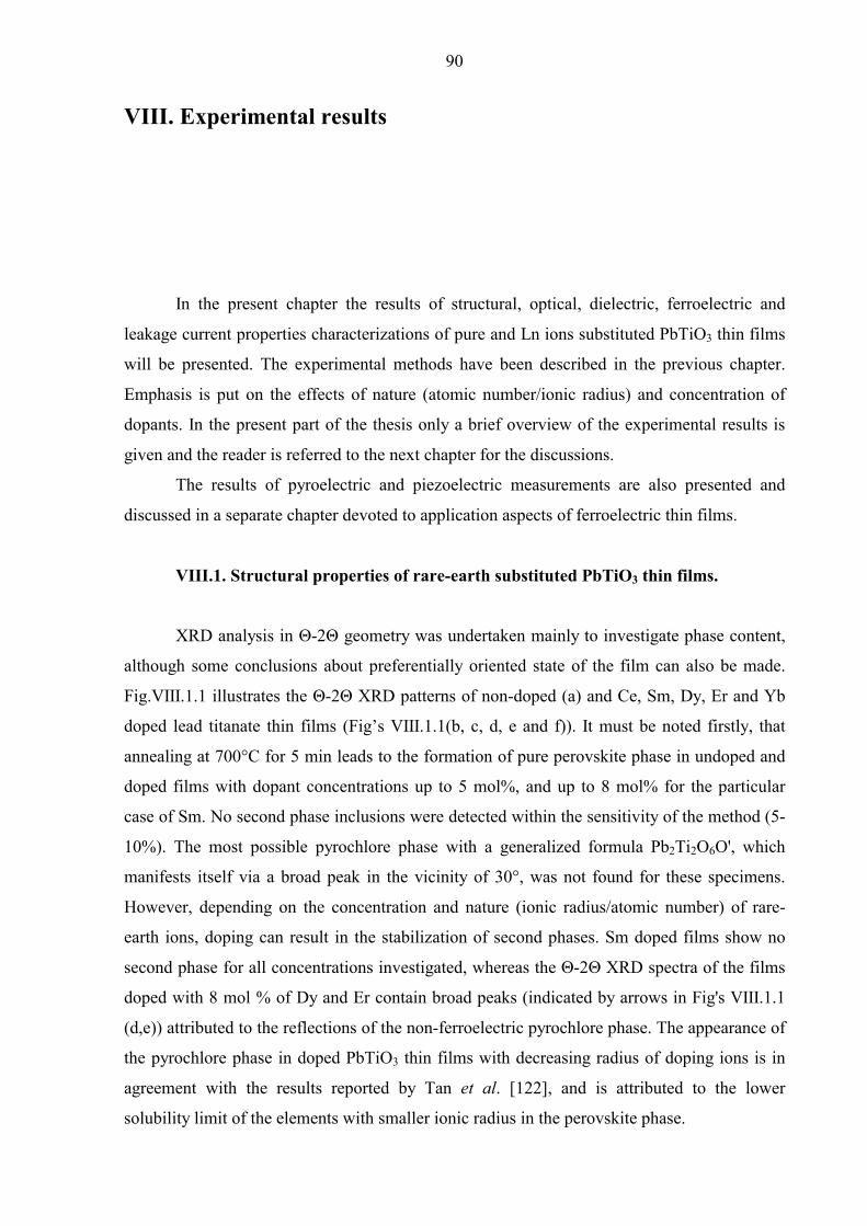
90
VIII. Experimental results
In the present chapter the results of structural, optical, dielectric, ferroelectric and
leakage current properties characterizations of pure and Ln ions substituted PbTiO3 thin films
will be presented. The experimental methods have been described in the previous chapter.
Emphasis is put on the effects of nature (atomic number/ionic radius) and concentration of
dopants. In the present part of the thesis only a brief overview of the experimental results is
given and the reader is referred to the next chapter for the discussions.
The results of pyroelectric and piezoelectric measurements are also presented and
discussed in a separate chapter devoted to application aspects of ferroelectric thin films.
VIII.1. Structural properties of rare-earth substituted PbTiO3 thin films.
XRD analysis in Θ-2Θ geometry was undertaken mainly to investigate phase content,
although some conclusions about preferentially oriented state of the film can also be made.
Fig.VIII.1.1 illustrates the Θ-2Θ XRD patterns of non-doped (a) and Ce, Sm, Dy, Er and Yb
doped lead titanate thin films (Fig’s VIII.1.1(b, c, d, e and f)). It must be noted firstly, that
annealing at 700°C for 5 min leads to the formation of pure perovskite phase in undoped and
doped films with dopant concentrations up to 5 mol%, and up to 8 mol% for the particular
case of Sm. No second phase inclusions were detected within the sensitivity of the method (5-
10%). The most possible pyrochlore phase with a generalized formula Pb2Ti2O6O', which
manifests itself via a broad peak in the vicinity of 30°, was not found for these specimens.
However, depending on the concentration and nature (ionic radius/atomic number) of rare-
earth ions, doping can result in the stabilization of second phases. Sm doped films show no
second phase for all concentrations investigated, whereas the Θ-2Θ XRD spectra of the films
doped with 8 mol % of Dy and Er contain broad peaks (indicated by arrows in Fig's VIII.1.1
(d,e)) attributed to the reflections of the non-ferroelectric pyrochlore phase. The appearance of
the pyrochlore phase in doped PbTiO3 thin films with decreasing radius of doping ions is in
agreement with the results reported by Tan et al. [122], and is attributed to the lower
solubility limit of the elements with smaller ionic radius in the perovskite phase.

91
20 25 30 35 40 45 50
Inte
nsity
, a.u
.
2Θ, °
(001
)/(10
0)
(101
)/(11
0) Pt(1
11)
(002
)/(20
0)
(a)PbTiO3
20 25 30 35 40 45 50
Inte
nsity
, a.u
.
2Θ, °
(001
)/(10
0)
(101
)/(11
0) Pt(1
11)
(002
)/(20
0)
(b)
2 mol % Ce
20 25 30 35 40 45 50
8 mol % Sm
2Θ, °
5 mol % Sm
Inte
nsity
, a.u
.
(002
)/(20
0)
Pt(1
11)
(101
)/(11
0)
2 mol % Sm
(001
)/(10
0) (c)
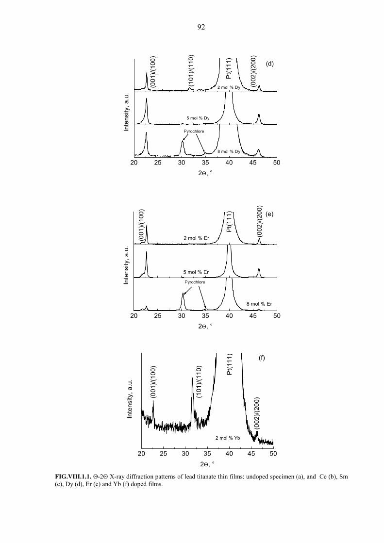
92
FIG.VIII.1.1. Θ-2Θ X-ray diffraction patterns of lead titanate thin films: undoped specimen (a), and Ce (b), Sm (c), Dy (d), Er (e) and Yb (f) doped films.
20 25 30 35 40 45 50
8 mol % Dy
Pyrochlore
2Θ, °
5 mol % Dy
Inte
nsity
, a.u
.
2 mol % Dy(101
)/(11
0)
Pt(1
11)
(002
)/(20
0)
(001
)/(10
0) (d)
20 25 30 35 40 45 50
8 mol % Er
2Θ, °
Pyrochlore
5 mol % Er
Inte
nsity
, a.u
.
(002
)/(20
0)
Pt(1
11)
(001
)/(10
0)
2 mol % Er
(e)
20 25 30 35 40 45 50
(101
)/(11
0)
(002
)/(20
0)
Pt(1
11)
(001
)/(10
0)
Inte
nsity
, a.u
.
2Θ, °
(f)
2 mol % Yb
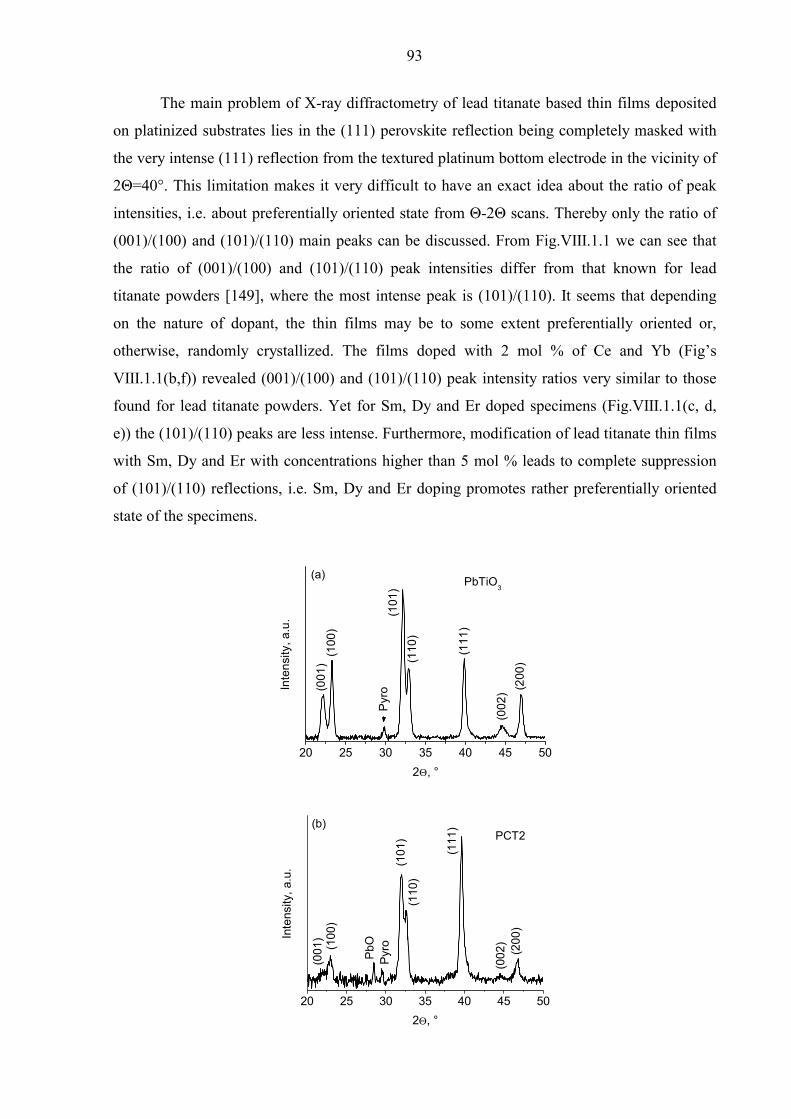
93
The main problem of X-ray diffractometry of lead titanate based thin films deposited
on platinized substrates lies in the (111) perovskite reflection being completely masked with
the very intense (111) reflection from the textured platinum bottom electrode in the vicinity of
2Θ=40°. This limitation makes it very difficult to have an exact idea about the ratio of peak
intensities, i.e. about preferentially oriented state from Θ-2Θ scans. Thereby only the ratio of
(001)/(100) and (101)/(110) main peaks can be discussed. From Fig.VIII.1.1 we can see that
the ratio of (001)/(100) and (101)/(110) peak intensities differ from that known for lead
titanate powders [149], where the most intense peak is (101)/(110). It seems that depending
on the nature of dopant, the thin films may be to some extent preferentially oriented or,
otherwise, randomly crystallized. The films doped with 2 mol % of Ce and Yb (Fig’s
VIII.1.1(b,f)) revealed (001)/(100) and (101)/(110) peak intensity ratios very similar to those
found for lead titanate powders. Yet for Sm, Dy and Er doped specimens (Fig.VIII.1.1(c, d,
e)) the (101)/(110) peaks are less intense. Furthermore, modification of lead titanate thin films
with Sm, Dy and Er with concentrations higher than 5 mol % leads to complete suppression
of (101)/(110) reflections, i.e. Sm, Dy and Er doping promotes rather preferentially oriented
state of the specimens.
20 25 30 35 40 45 50
Inte
nsity
, a.u
.
2Θ, °
(001
)(1
00)
Pyro
(101
)(1
10)
(111
)
(002
) (200
)
(a) PbTiO3
20 25 30 35 40 45 50
Inte
nsity
, a.u
.
2Θ, °
(b)
(001
)(1
00)
Pyro
(101
)(1
10)
(111
)
(002
)(2
00)
PbO
PCT2

94
20 25 30 35 40 45 50
2Θ, °
PST8
Inte
nsity
, a.u
. PST5
PbO orSm2O3
PST2(c)
(001
)/(10
0)
Pyro
(101
)/(11
0)
(111
)
(002
)/(20
0)
20 25 30 35 40 45 50
2Θ, °
PDT8
Inte
nsity
, a.u
. PDT5
PDT2(d)
(001
)/(10
0)
Pyro
(101
)/(11
0)
(111
)
(002
)/(20
0)

95
FIG.VIII.1.2. GI XRD patterns obtained for pure (a) and Ce (b), Sm (c), Dy (d), Er (e) and Yb (f) doped PbTiO3 thin films.
Fig. VIII.1.2 shows the results of GI XRD characterization. It must be stressed that
while Θ-2Θ scans showed only the existence of the perovskite phase in pure and films doped
with 2 mol % of Ce, Dy, Er and Yb, and 2-8 mol % of Sm, GI experiments revealed small
amounts of second phases along with the perovskite phase for the specimens of all
compositions investigated. The spectra obtained by GI geometry clearly show peaks in the
vicinity of 29° which were attributed to the pyrochlore phase. Additionally, the modification
of the films with Sm and Ce was found to result in the formation of lead oxide (the
corresponding peaks are clearly seen on Fig's VIII.1.2 (b,c)). The discrepancy between the
XRD data obtained in Θ-2Θ and GI configurations is caused by the basic difference between
20 25 30 35 40 45 50
2Θ, °
PET8
Inte
nsity
, a.u
. PET5
(001
)/(10
0)
Pyro
(101
)/(11
0)
(111
)
(002
)/(20
0)
PET2(e)
20 25 30 35 40 45 50
Inte
nsity
, a.u
.
2Θ, °
(f)
(001
)/(10
0)
Pyro
(101
)(1
10)
(111
)
(002
)(2
00)PYT2

96
these two techniques. Comparison of the XRD data obtained in Θ-2Θ and GI geometries will
be considered in the next chapter (see "Discussions").
The lattice parameters of the tetragonal lattice, a and c, can be calculated from the
angular positions Θ1 and Θ2 of any splitted pair of peaks with indices (h1k1l1) and (h2k2l2)
using familiar equations
2 2 2 2 2 222 2 1 1 1 2 2
2 2 2 22 1 1 2
2 2 2 2 2 222 2 1 1 1 2 2
2 2 2 2 2 21 1 2 2 2 1
( ) ( )4 sin sin
( ) ( )4 ( )sin ( )sin
l h k l h kal l
l h k l h kch k h k
λ
λ
+ − +=Θ − Θ
+ − +=+ Θ − + Θ
(VIII.1.1)
where λ is the wavelength of X-rays. The tetragonality factor, c/a, is therefore
2 2 2 22 1 1 2
2 2 2 2 2 21 1 2 2 2 1
sin sin( )sin ( )sin
l lca h k h k
Θ − Θ=+ Θ − + Θ
(VIII.1.2)
The tetragonal distortion was determined from XRD GI experiments (Fig. VIII.1.3). Position
of high-angular pair of peaks found from Gaussian fitting to the experimental data was taken.
It can be seen that the c/a decreases with increasing concentration of doping elements.
FIG.VIII.1.3. Tetragonal strain, c/a, calculated from GI scans of Ce, Sm, Dy, Er and Yb doped lead titanate thin films. The data are plotted vs. doping level (in mol %).
Fig.VIII.1.4 represents the (100) pole figures measured for pure (a) and doped PbTiO3
thin films with 5 mol % of Er (b) and 8 mol % of Sm (c). The data demonstrate that doping
with various RE's leads to specific effects on the orientation of the films. While Er (small
ionic radius) practically has no effect on the texture of PbTiO3 which shows as strong (100)
out of plane orientation, as evidenced by the pole figure in Fig’s VIII.1.4(a) and (b), the pole
distribution density of Sm (ionic radius greater than that of Er) substituted PbTiO3 thin film
(Fig. VIII.1.4(c)) is found to be mainly concentrated in the ring at approximately Chi=54°
0 2 4 6 81.020
1.025
1.030
1.035
1.040
1.045
1.050
1.055
c/a
x, mol %
Ce Sm Dy Er Yb none

97
which corresponds to the angle between the [100] and [111] directions of the pseudo-cubic
perovskite lattice. No in-plane texture is revealed.
FIG.VIII.1.4. (100) Pole figures obtained for pure (a) and doped PbTiO3 films: 5 mol % of Er (b) and 8 mol % of Sm (c).
Fig.VIII.1.4 shows that the present films crystallize with the formation of fibre texture,
usually found for the majority of thin films deposited onto polycrystalline substrates via sol-
gel (a uniform pole density distribution with respect to the azimuthal angle, Phi, indicates the
fibre or uniaxial character of the texture). Fig.VIII.1.5 shows (100) FT plots of lead titanate
thin films doped with various amounts of Sm and Er. The data obtained for the undoped film
are also shown for comparison. It is important to note that already a relatively small
concentration of 2 mol% of doping elements dramatically affects the texture of the films, and
that a further increase of doping ions concentration did not affect noticeably the preferred
orientation of the films (Fig.VIII.1.5).
0 15 300
15
30
45
60
75
(a)
Chi, °
Chi
, °
Phi0°
90°
0 15 30
(b)
0 15 30 45 60 750
15
30
45
60
75
(c)

98
FIG.VIII.1.5. (100) Fibre texture plots obtained for Sm- and Er-substituted thin films. Numbers indicate the doping level (in mol %).
FIG.VIII.1.6. (100) Fibre texture plots obtained for pure PbTiO3 (a) and 2 mol % of Ce (b), Sm (c), Dy (d), Er (e) and Yb (f) doped thin films.
Fig. VIII.1.6 illustrates the (100) FT plots of pure PbTiO3 films and films doped with 2
mol % of RE’s. The results reported in the present work demonstrate unambiguously that the
development of preferred orientations of the films is very sensitive to the type of substituent
RE and, to a lesser extent, to the doping level. At the same time, no apparent correlation
-80 -40 0
Er-series
8
52
0
Inte
nsity
, arb
.uni
ts
Chi, °
0
2
5
8
Sm-series
-80 -40 0
(a)
(b)
Inte
nsity
, arb
. uni
ts
(c)
(d)
-80 -60 -40 -20 0 20
(e)
-80 -60 -40 -20 0 20
Chi, °
(f)

99
between preferred orientation formation and atomic numbers/ionic radii of doping ions (and
hence lattice parameters) is found.
VIII.2. Raman scattering from pure and rare-earth substituted PbTiO3 thin
films.
Raman spectra of 2 mol % of RE substituted PbTiO3 thin films are demonstrated in
Fig. VIII.2.1. The modes were labelled according to the nomenclature proposed by Burns and
Scott [81,82]. It can be seen that the Raman spectra contain all bands reported for PbTiO3
bulk materials and thin films by other groups in the frequency range investigated (see
paragraph V.3 and references sited therein). The results indicate that the films are well
crystallized into the tetragonal perovskite phase.
FIG.VIII.2.1. Room temperature Raman spectra of pure PbTiO3 and doped with 2 mol % of Ce, Sm, Dy, Er and Yb thin films. Raman modes are indicated by letters: A – E(1TO), B – A1(1LO)+E(2TO), C – B1+E (silent), D – A1(2TO), E – E(2LO)+A1(2LO), F – E(3TO), G – A1(3TO).
FIG.VIII.2.2. Room temperature Raman spectra of lead titanate thin films doped with various amounts of Er.
0 100 200 300 400 500 600 700 800
Inte
nsity
, a.u
.
Raman shift, cm-1
2
5
8
0
E(1TO)
100 200 300 400 500 600 700
G
FE
D
C ErDy
SmCe
Inte
nsity
, a.u
.
Raman shift, cm-1
PbTiO3A
B
Yb
100
It was found that the Raman spectra of the films doped with the elements of lanthanide
series are characterised with more feebly marked Raman bands in comparison to the undoped
films. This is exemplified in Fig. VIII.2.2 where the Raman spectra obtained for the
specimens substituted with 2, 5 and 8 mol % of Er are shown. It must be noted that with
increasing Er concentration the lines become broader and their intensities decrease.
Furthermore, it can be inferred from the lowering of E(1TO) soft mode frequency that doping
with the lanthanide elements leads to weakening of the ferroelectric order (E(1TO) transverse
optical phonon is known to be coupled with the displacement of cation within the oxygen
octahedron). Fig.VIII.2.3. shows typical dependence of E(1TO) soft modes on doping level
found for Dy (a) and Er (b) modified films.
FIG.VIII.2.3. Position of E(1TO) soft modes obtained for Dy (a) and Er (b) substituted PbTiO3 films and plotted vs. doping level.
VIII.3. Refractive indices and extinction coefficients of lanthanide ions doped
lead titanate thin films.
Fig.VIII.3.1 shows, how the refractive indices n (a) and the extinction coefficients k
(b) of 2 mol % of Ln doped films change with respect to the nature of doping element in
comparison to non-doped specimen. A high value of n (2.73 at λ=632.8 nm) was obtained for
pure lead titanate thin film (compare to n=2.66 reported for PbTiO3 bulk specimen at the same
wavelength [150]). At the same time, the refractive index of our PT film is higher than that
obtained by Wood et al. [70] (see Table V.1.1) for a film of nearly the same thickness
deposited on sapphire substrate. For rare-earth doped PbTiO3 films one can note some
decrease in n. Moreover, with exception of Ce, the trend of n to decrease from 2.69 to 2.57
when the atomic number of the element changes from 62 (Sm) to 70 (Yb) can be observed.
Furthermore, Ce and Sm doping lead to the reduction of k, whereas Dy, Er and Yb doped
0 1 2 3 4 5 6 7 8 977
78
79
80
81
82
Ram
an s
hift,
cm
-1
Er content, mol %
(b)
0 1 2 3 4 5 6 7 8 974
75
76
77
78
79
80
81
82
Ram
an s
hift,
cm
-1
Dy content, mol %
(a)

101
specimens show an increase in the extinction coefficient, in comparison to pure PbTiO3. The
smallest value of k (2.11*10-4) was found for the film, doped with 2 mol % of Ce.
The refractive indices and extinction coefficients of Sm, Dy, Er and Yb doped films
are plotted vs. doping level in Fig.VIII.3.2. For both Sm and Dy some decrease in the index of
refraction is observed (Fig.VIII.3.2(a)) which is in contradiction to the results reported by
FIG.VIII.3.1. Values of the refractive index n (a), and the extinction coefficient k (b) for PbTiO3 thin films doped with 2 mol % of lanthanide elements.
FIG.VIII.3.2. Values of refractive index n (a), and extinction coefficient k (b) of Sm, Dy, Er and Yb doped PbTiO3 thin films plotted vs. concentration of the doping ions. Chang and Desu [72] for La and Nd doped PZT thin films. In contrast, doping with 5 and 8
mol % of Er did not produce any noticeable effect. The imaginary part of the refractive index
(the extinction coefficient) of Sm, Dy and Er doped films revealed a complex behaviour with
0 2 4 6 8
1.6
1.8
2.0
2.2
2.4
2.6
2.8
Ce Sm Dy Er Yb none
n
x
(a)
0 2 4 6 8
0.00
0.01
0.02
0.03
0.04
0.05
0.06 Ce Sm Dy Er Yb none
k
x
(b)
0 60 64 68 72
2.50
2.55
2.60
2.65
2.70
2.75
n
(a)
0 60 64 68 72-0.005
0.000
0.005
0.010
0.015
0.020
0.025
0.030
0.035
0.040(b)
k
Atomic number
none
Ce
Sm
Dy
ErYb
none
CeSm
Dy
Er
Yb

102
respect to the doping level. For all concentrations investigated, Dy and Er doped films show
near linear increase of k when the doping level increases (Fig.VIII.3.2(b)), whereas doping
with Sm leads to the opposite effect – the extinction coefficient, which describes damping of
the light intensity, was slightly decreased for x<5 mol 5 %. Further increase in Sm content
caused an abrupt increase in k.
In order to elucidate the specific effect of Ce on the optical properties of lead titanate
thin films, XPS spectra were obtained for lead titanate thin films substituted with 5 mol % of
Ce. The results are presented in Fig. VIII.3.3(a,b). The spectra are obtained for as-deposited
films and after Ar-ion cleaning of the surface. Fig.VIII.3.3(b) represents the detailed structure
of the peak which can attributed to Ce in its oxidation state of +4. The results will be
discussed in the following (see "Discussions").
FIG.VIII.3.3. XPS spectra of PbTiO3 thin film doped with 5 mol % of Ce (a). Here the peaks denoted as: a and b-Ce 3d5/2, c-Ce Auger, d-Pb 4p1/2, e-Pb 4p3/2, f-Ti 2s, g-O 1s, h-Ti 2p1/2, 2p3/2, i-Pb 4d3/2, j-Pb 4d5/2, k-C 1s, l-Pb 4f5/2, and m-Pb 4f7/2. The spectrum of as-deposited film is shown by dashed line. Solid line represents the spectrum taken after cleaning of the surface with Ar ions at 1 kEv, 70 nA for 2 min. Detailed structure of the peak which attributed to 3d5/2 of Ce is shown separately (b). The experimental data are shown by circles; the result of the Gaussian fitting is represented by the solid line.
800 600 400 200
(a)
i
Inte
nsity
, a.u
.
Binding energy, eV
a bc d
e f
g
hj
k
l m
888 884 880 876 872
Ce 3d5/2877 eV
Inte
nsity
, a.u
.
Binding energy, eV
881 eV(b)

103
VIII.4. Room temperature dielectric properties of pure and doped lead titanate
thin films.
The room temperature dielectric properties (ε′, tanδ) of lead titanate thin films doped
with Ce, Sm, Dy, Er and Yb were investigated. To analyse doping effects on the dielectric
properties, metal-ferroelectric-metal configuration was treated as a conventional plane
capacitor, and the dielectric constant was obtained from the measured value of capacitance, C,
using:
0 'SCd
ε ε= (VIII.4.1)
ε0 is the dielectric permittivity of free space, S the area of the pad and d the film thickness
(ellipsometric). Ten pads were measured for each specimen in order to estimate the error.
Fig.VIII.4.1 shows, how the dielectric properties of PbTiO3 thin films correlate with the
FIG.VIII.4.1. Room temperature dielectric constant, ε′ (a), and tanδ (b) of lead titanate thin films doped with 2 mol % of Ln-elements. Measurements were conducted at 1 kHz with the amplitude of ac signal 50 mVp-p.
nature of dopant for a doping level of 2 mol%. We must note that irrespective of the atomic
number of lanthanide element, both the dielectric constant and loss tangent increase in
comparison to pure lead titanate thin film. Furthermore, the value of ε′ and tanδ correlate
with the atomic number of dopant. It can be seen that both ε′ and tanδ increase smoothly from
228 and 0.03 respectively for pure PbTiO3 up to 371 and 0.087 for the specimen doped with 2
mol % of Yb. The dielectric properties of Ce, Sm, Dy, Er and Yb doped specimens are plotted
0 60 64 68 72
240
280
320
360Yb
ErDy
SmCe
ε'
none
(a)
0 60 64 68 72
0.03
0.04
0.05
0.06
0.07
0.08
0.09
(b)
Yb
Er
DySm
Cenone
tan δ
Atomic number

104
vs. doping level in Fig.VIII.4.2 (see Fig.VIII.4.1 for the error bars). For doping element
concentrations up to 5 mol % it can be noticed that ε′ generally increases with increasing
doping level. Higher concentrations lead for Sm and Er doped films to lower ε′ whereas the
values of Dy doped films continue to increase. The loss factor is found to increase in the case
of Sm and Er doped samples for concentrations lower than 5 mol % and decrease for
concentrations higher than 5 mol %. Dy substituted films show a maximum of tanδ at x = 0.02
(2 mol %).
FIG.VIII.4.2. ε′ (a) and tanδ (b) of lead titanate thin films doped with Ce, Sm, Dy, Er and Yb plotted vs. doping level, x (given in mol %).
VIII.5. Effect of lanthanide ions doping on the ferroelectric-paraelectric phase
transition temperature.
The temperature dependence of the small signal dielectric properties of pure and Ce,
Sm, Dy and Er doped PbTiO3 thin films were characterized on cooling at various frequencies
and 50 mVp-p driving signal. ε′(T) dependencies of all specimens investigated have shown
characteristic maxima which are attributed to the paraelectric-to-ferroelectric phase transition.
The experimental results are presented in Fig.VIII.5.1. The values of TC were obtained from
the positions of the maxima of the ε′(T) curves. No frequency dependence of TC was found
(nonrelaxor-type) for all doping elements and concentrations. Fig.VIII.5.2 shows that TC
correlates with the atomic number of doping elements (2 mol % doping level). It must be
stressed firstly that non-doped PbTiO3 thin films (Fig’s.VIII.5.1 and VIII.5.2) revealed
paraelectric-to-ferroelectric phase transition at a much lower temperature than that reported
for bulk specimen (compare TC (PbTiO3 ceramics) = 490°C [p.12 in ref.8] vs. 450°C, found
for our film). Generally, doping with lanthanide elements leads to a smooth decrease of TC
with increasing atomic number. The dependence of TC on doping level is shown in
0 2 4 6 8200
240
280
320
360
400 1 kHz; 50 mVp-p
ε '
x
Ce Sm Dy Er Yb none (a)
0 2 4 6 80.02
0.04
0.06
0.08
0.10
0.12
0.14
0.16
tan δ
x
Ce Sm Dy Er Yb none
(b)

105
FIG.VIII.5.1. Temperature dependent dielectric constant of non-doped PbTiO3 thin film (a), and doped with Ce (b)(2 mol %), Sm (c), Dy (d) and Er (e), measured on cooling with the amplitude of AC driving signal 50 mVp-p and frequency 1 kHz.
FIG.VIII.5.2. Curie transition temperature of lead titanate thin films, doped with 2 mol % of Ce, Sm, Dy and Er. Measurements were performed on cooling with the amplitude of driving signal 25 mV.
0 56 58 60 62 64 66 68 70
380
400
420
440
460
T C, °
C
Atomic number
noneCe
Sm
DyEr
200 250 300 350 400 450 5000
200
400
600
800
ε'
T, °C
(a)
300 350 400 450 500
300
400
500
600
700
800
ε'
T, °C
(b)
200 250 300 350 400 450
400
600
800
1000
1200
1400
1600
PST2 PST5 PST8
ε'
T, °C
(c)
200 250 300 350 400 450300
600
900
1200
1500
1800
2100 PDT2 PDT5 PDT8
ε'
T, °C
(d)
200 300 400 500200
400
600
800 PET2 PET5 PET8
ε'
T, °C
(e)

106
FIG.VIII.5.3. Curie transition temperature of Ln ions doped specimens, plotted vs. doping level.
Table VIII.5.1. Curie transition temperature of lanthanide elements doped PbTiO3 thin films obtained from ε′(T) measurements.
dopant
concentration, mol %
none Ce Sm Dy Er
0 450 - - - - 2 - 444 425 410 400 5 - - 410 405 395 8 - - 367 352 365
FIG.VIII.6.1. P-E hysteresis loops measured for PbTiO3 thin films doped with 2 mol % of Ce (a) and 2, 5 and 8 mol % of Sm (b), Dy (c) and Er (d). The hysteresis characteristics were acquired at room temperature with square pulses modulated with time 0.13 ms.
0 2 4 6 8
360
400
440
T c,
°C
x
Ce Sm Dy Er none
-400 -200 0 200 400-60
-40
-20
0
20
40
P, µ
C/c
m2
E, kV/cm
PbTiO3
PCT2
(a)
-450 -300 -150 0 150 300 450-60
-40
-20
0
20
40
60
P, µ
C/c
m2
E, kV/cm
PbTiO3
PST2 PST5 PST8
(b)
-400 -200 0 200 400-60
-40
-20
0
20
40
PbTiO3
PDT2 PDT5 PDT8
P, µ
C/c
m2
E, kV/cm
(c)
-400 -200 0 200 400-60
-40
-20
0
20
40
PbTiO3
PET2 PET5 PET8 (520 nm, ref. 72)
P, µ
C/c
m2
E, kV/cm
(d)
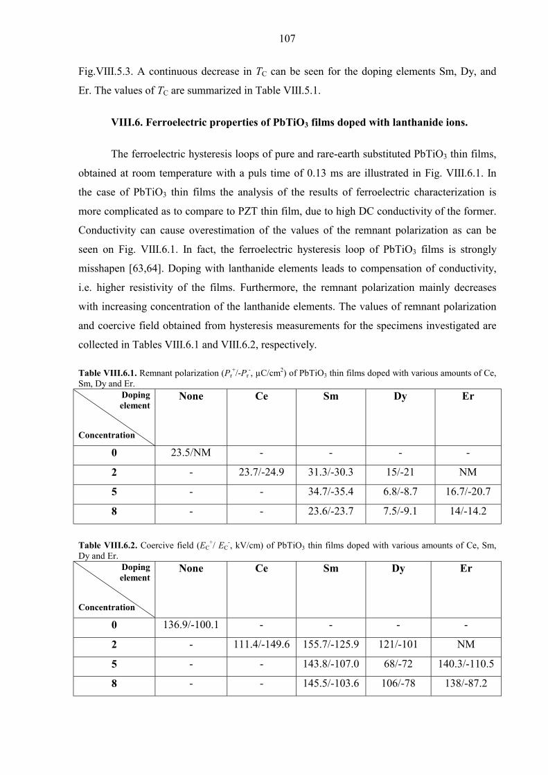
107
Fig.VIII.5.3. A continuous decrease in TC can be seen for the doping elements Sm, Dy, and
Er. The values of TC are summarized in Table VIII.5.1.
VIII.6. Ferroelectric properties of PbTiO3 films doped with lanthanide ions.
The ferroelectric hysteresis loops of pure and rare-earth substituted PbTiO3 thin films,
obtained at room temperature with a puls time of 0.13 ms are illustrated in Fig. VIII.6.1. In
the case of PbTiO3 thin films the analysis of the results of ferroelectric characterization is
more complicated as to compare to PZT thin film, due to high DC conductivity of the former.
Conductivity can cause overestimation of the values of the remnant polarization as can be
seen on Fig. VIII.6.1. In fact, the ferroelectric hysteresis loop of PbTiO3 films is strongly
misshapen [63,64]. Doping with lanthanide elements leads to compensation of conductivity,
i.e. higher resistivity of the films. Furthermore, the remnant polarization mainly decreases
with increasing concentration of the lanthanide elements. The values of remnant polarization
and coercive field obtained from hysteresis measurements for the specimens investigated are
collected in Tables VIII.6.1 and VIII.6.2, respectively. Table VIII.6.1. Remnant polarization (Pr
+/-Pr-, µC/cm2) of PbTiO3 thin films doped with various amounts of Ce,
Sm, Dy and Er. Doping element
Concentration
None Ce Sm Dy Er
0 23.5/NM - - - -
2 - 23.7/-24.9 31.3/-30.3 15/-21 NM
5 - - 34.7/-35.4 6.8/-8.7 16.7/-20.7
8 - - 23.6/-23.7 7.5/-9.1 14/-14.2
Table VIII.6.2. Coercive field (EC+/ EC
-, kV/cm) of PbTiO3 thin films doped with various amounts of Ce, Sm, Dy and Er.
Doping element
Concentration
None Ce Sm Dy Er
0 136.9/-100.1 - - - -
2 - 111.4/-149.6 155.7/-125.9 121/-101 NM
5 - - 143.8/-107.0 68/-72 140.3/-110.5
8 - - 145.5/-103.6 106/-78 138/-87.2

108
FIG.VIII.6.2. Ferroelectric hysteresis loop of PbTiO3+5 mol % Er thin film (195 nm thickness) deposited on LNO bottom electrode.
Fig.VIII.6.2 exemplifies the room temperature P-E characteristic obtained for lead
titanate thin film doped with 5 mol % of Er and deposited onto LNO bottom electrode.
Utilization of lanthanum nickel oxide as the bottom electrode material lead to poorly saturated
ferroelectric hysteresis loop (as to compare to that measured for the film of the same
composition deposited on Pt, Fig.VIII.6.1(d), and low remnant polarization. The results
obtained will be discussed in details in the next chapter.
VIII.7. Thickness effects and contribution of interfacial bottom electrode-thin
film layer into small signal dielectric properties of doped lead titanate thin films.
The capacity of PET5 thin films was investigated systematically as a function of film
thickness and type of the electrode. Correlation of the dielectric constant with the film
thickness is a particular feature of dielectric thin films. As already mentioned, various factors,
such as stress which could be developed during high temperature treatment of thin films and
subsequent cooling through Curie temperature, chemical interaction between film and
electrode material may lead to the formation of interfacial zones characterized by dielectric
properties different from those of the interior parts of the film (see paragraph V.4 and
references sited therein). According to the widely accepted model of metal-ferroelectric-metal
structure, the whole structure is treated as a ferroelectric bulk capacitor with a capacity Cb in
series with an interfacial capacitor between the electrode and ferroelectric bulk with a
capacity Ci. It is assumed that (i) interfacial (disturbed) layer is characterized with smaller
dielectric constant compared to that of the interior part of the film and (ii) the interfacial layer
is thin compared to the whole thickness of the capacitor. The measured capacity C of the
MFM structure can be expressed as follows [93]:
-400 -200 0 200 400
-30
-20
-10
0
10
20
30
P, µ
C/c
m2
E, kV/cm

109
0
1 1 1 1'b i apparent i
dC C C S Cε ε
= + = + (VIII.7.1)
According to this model, the thickness dependence of the reciprocal of the measured
capacity must show a linear behaviour. The experimental of the reciprocal of the capacity of
PET5 thin films deposited on Pt and LNO bottom electrodes vs. thickness shown in
Fig.VIII.7.1.reveal that the model has only a limited applicability.
FIG.VIII.7.1. Reciprocal of capacitance of PET5 thin films deposited on platinum (squares) and LNO (cirsles) bottom electrodes (1 kHz, 50 mVp-p). Data plotted vs. film thickness.
VIII.8. Field-dependent dielectric properties of pure and doped lead titanate thin films.
The room temperature ε′-E characteristics obtained for pure and Sm and Er doped thin
films are shown in Fig’s VIII.8.1 and VIII.8.2. The directions of the DC bias sweep are
indicated by arrows.
FIG.VIII.8.1. ε′-E characteristics, obtained at room temperature for pure and Sm (2 and 5 mol %) substituted film. Frequency and amplitude of ac measuring signal were 5 kHz and 50 mVp-p, respectively.
150 200 250 300 350 400 450
3x10⁸
4x10⁸
5x10⁸
6x10⁸
7x10⁸
8x10⁸
9x10⁸
1/C
, 1/F
d, nm
PET5 on LNO buffer layer linear fit
C-1 =3.78*10
7 +1.37*106 d
PET5 on Pt electrode
-400 -200 0 200 400
100
150
200
250
300
350 pure PbTiO3
2 mol % Sm 5 mol % Sm
ε'
E, kV/cm

110
FIG.VIII.8.2. ε′-E characteristics, obtained at room temperature for pure and Er (2 and 5 mol %) substituted film. Frequency and amplitude of ac measuring signal were 5 kHz and 50 mVp-p, respectively.
FIG.VIII.8.3. Contribution of domain walls oscillation, η, into the dielectric constant and built-in field, EB, calculated from data presented in Fig’s VIII.8.1 and VIII.8.2.
The “butterfly”-like shape of ε′-E plots is the characteristic of ferroelectric material
where the relative permittivity reaches its maximum in the vicinity of the coercive field. One
can note that the ε′-E curves are non-symmetric both with respect to ε′ and E axes. As
mentioned above, non-linear response of ε′ with respect to the applied DC bias reflects the
contribution of domain walls oscillation to the value of the dielectric constant. Considering
the crystallites are being in monodomain state at high DC bias (higher than the coercive field),
it is possible to estimate the contribution of domains to the measured value of ε′ in percentage
ratio. Assuming the monodomain state of the grains at E=400 kV/cm (corresponds to
maximum applied field during the experiment), we estimated contribution of domains, η, to ε′
as [(ε′max-ε′400)/ ε′max]·100% (ε′max was obtained from the part of ε′-E curve corresponding to
positive DC bias sweep). Furthermore, the value of the built-in field (shift of ε′-E along E-
axis), EB, was calculated as ( ) / 2B c cE E E+ −= + , where Ec+ and Ec
- are positive and negative
coercive fields, found from the positions of corresponding peaks (Fig’s VIII.8.1 and VIII.8.2).
The values of η and Eb calculated from ε′-E curves of pure and doped (2 and 5 mol % of Sm
-400 -200 0 200 400150
200
250
300
ε '
E, kV/cm
pure PbTiO3
2 mol % Er 5 mol % Er
0 1 2 3 4 5
30
35
40
45
50
55
60
65
-2024681012141618
η (Sm) η (Er)
η , %
Doping level, mol %
E B, k
V/c
m
EB (Sm) EB (Er)

111
and Er) films are represented in Fig.VIII.8.3. A general trend to reduce the built-in field was
found for both Sm and Er. At the same time, the contribution of domain walls to the dielectric
constant, η, increased for Sm substituted specimens and remained unaffected in Er substituted
specimens (Fig.VIII.8.3).
Fig.VIII.8.4 demonstrates the room temperature ε′-E characteristics obtained for 5
mol% of Er substituted films deposited on Pt and LNO bottom electrodes. The positive and
the negative coercive fields, the built in field, the maximum values of the dielectric constant
(corresponding to EC) and the contribution of domain structure to the measured value of the
dielectric constant obtained from ε′-E characteristics are summarized in Table VIII.8.1. It can
be seen that the use of LNO as bottom electrode caused, on one hand, development of a built-
in field and, on the other hand noticeable broadening of the peaks.
FIG.VIII.8.4. Comparison of ε′-E characteristics of PET5 thin films, deposited on Pt and LNO bottom electrodes. Dielectric constant was measured at room temperature with the frequency of AC signal 1 kHz and the amplitude 50 mVp-p.
Table VIII.8.1. Ferroelectric and dielectric properties, obtained from ε′-E characteristics, shown in Fig.VIII.8.4.
VIII.9. Voltage-, temperature- and thickness-dependent leakage currents in pure
and doped lead titanate thin films.
As already mentioned analysis of the mechanisms responsible for charge transport in
dielectric thin films is rather difficult, since different processes can contribute to the measured
value of current density in the same range of temperatures or applied voltages. A
Measured structure
Ec-,
kV/cm Ec
+, kV/cm
Eb, kV/cm
ε′m+ ε′m- η, %
Pt/PET5/Pt -107 108 0.5 304 322 49
Pt/PET5/LNO/Pt -68 128 30 220 214 26
-400 -200 0 200 400
160
240
320
ε '
E, kV/cm
on Pton LNO
1 kHz, 50 mVp-p
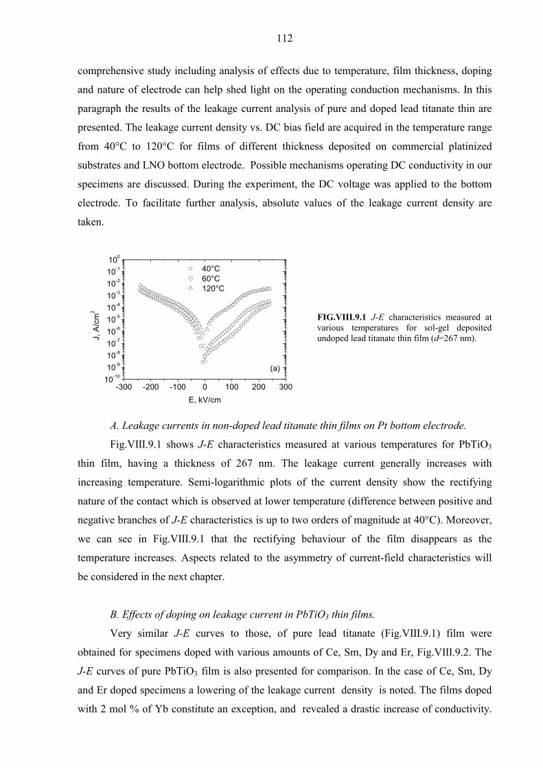
112
comprehensive study including analysis of effects due to temperature, film thickness, doping
and nature of electrode can help shed light on the operating conduction mechanisms. In this
paragraph the results of the leakage current analysis of pure and doped lead titanate thin are
presented. The leakage current density vs. DC bias field are acquired in the temperature range
from 40°C to 120°C for films of different thickness deposited on commercial platinized
substrates and LNO bottom electrode. Possible mechanisms operating DC conductivity in our
specimens are discussed. During the experiment, the DC voltage was applied to the bottom
electrode. To facilitate further analysis, absolute values of the leakage current density are
taken.
FIG.VIII.9.1 J-E characteristics measured at various temperatures for sol-gel deposited undoped lead titanate thin film (d=267 nm).
A. Leakage currents in non-doped lead titanate thin films on Pt bottom electrode.
Fig.VIII.9.1 shows J-E characteristics measured at various temperatures for PbTiO3
thin film, having a thickness of 267 nm. The leakage current generally increases with
increasing temperature. Semi-logarithmic plots of the current density show the rectifying
nature of the contact which is observed at lower temperature (difference between positive and
negative branches of J-E characteristics is up to two orders of magnitude at 40°C). Moreover,
we can see in Fig.VIII.9.1 that the rectifying behaviour of the film disappears as the
temperature increases. Aspects related to the asymmetry of current-field characteristics will
be considered in the next chapter.
B. Effects of doping on leakage current in PbTiO3 thin films.
Very similar J-E curves to those, of pure lead titanate (Fig.VIII.9.1) film were
obtained for specimens doped with various amounts of Ce, Sm, Dy and Er, Fig.VIII.9.2. The
J-E curves of pure PbTiO3 film is also presented for comparison. In the case of Ce, Sm, Dy
and Er doped specimens a lowering of the leakage current density is noted. The films doped
with 2 mol % of Yb constitute an exception, and revealed a drastic increase of conductivity.
-300 -200 -100 0 100 200 30010-1010-910-810-710-610-510-410-310-210-1100
J, A
/cm
2
E, kV/cm
40°C 60°C 120°C
(a)

113
The leakage current in this specimen could not be characterized due to device limitation. The
films substituted with 2 mol % of Ce demonstrated some degradation of the resistance at a
positive bias (applied to the bottom electrode) of approximately 200 kV/cm (Fig.VIII.9.2(a)).
Furthermore, a rather complex dependence of the leakage current density on the doping level
was revealed for the positive branches of the J-E curves obtained for Er substituted films
(Fig.VIII.9.2.(c)).
FIG.VIII.9.2. J-E characteristics obtained at 40°C for the films substituted with various amounts of Ce (a), Sm (b), Dy (c) and Er (d).
FIG.VIII.9.3. J-E characteristics, obtained at various temperatures for PET5 thin films, deposited on LNO (a) and Pt (b) bottom electrodes.
-400 -300 -200 -100 0 100 200 30010-9
10-7
10-5
10-3
pure PbTiO3
+2 mol % Ce
J, A
/cm
2
E, kV/cm
(a)
-300 -200 -100 0 100 200 30010-10
10-8
10-6
10-4
10-2
J, A
/cm
2
E, kV/cm
PbTiO3
+ 2 mol % Sm + 8 mol % Sm
(b)
-300 -200 -100 0 100 200 30010-9
10-7
10-5
10-3
J, A
/cm
2
E, kV/cm
PbTiO3
+ 2 mol % Dy + 8 mol % Dy
(c)
-300 -200 -100 0 100 200 300
10-8
10-6
10-4
10-2
PbTiO3
+ 2 mol % Er + 8 mol % Er
J, A
/cm
2
E, kV/cm
(d)
-400 -200 0 200 40010-9
10-8
10-7
10-6
10-5
10-4
10-3
J, A
/cm
2
E, kV/cm
40°C 60°C 80°C 100°C
(a)
-300 -200 -100 0 100 200 300 40010-10
10-9
10-8
10-7
10-6
10-5
10-4
10-3
J, A
/cm
2
E, kV/cm
40°C 60°C 80°C 100°C (b)

114
C. Influence of the electrode material on leakage current of lead titanate films.
For the purpose of investigating the contribution of the nature of the bottom electrode
and interfacial properties to the conductivity of ferroelectric thin films, the J-E characteristics
of films fabricated on platinum and lanthanum nickel oxide bottom electrodes were compared.
Fig's VIII.9.3 (a) and (b) show the J-E curves obtained at various temperatures for lead
titanate thin films doped with 5 mol % of deposited on LNO and Pt, respectively. It can be
seen that the use of conductive oxide (in particular, LNO) as bottom electrode did not produce
noticeable effects on the value of leakage current density, J (see also next section).
FIG.VIII.9.4. Thickness dependent leakage current density of PET5 thin films measured for films deposited on Pt (a) and LNO (b) bottom electrodes. The data are selected for applied DC bias corresponding to 3V. Experimental results are represented by symbols. Results of linear fitting are shown by straight lines and slopes are indicated by the numbers.
D. Effect of film thickness on leakage current in doped lead titanate thin films,
deposited on Pt and LNO bottom electrodes.
The leakage current densities were measured at various temperatures for PET5 films
of thicknesses from 200 to 390 nm. Both Pt and LNO bottom electrodes were considered. The
results are presented in Fig.VIII.9.4 in log-log plots for an applied DC bias of 3 V. As we
already mentioned in the paragraph V.8, the SCLC mechanism is characterized by the specific
J~d-m relation. The Thickness exponent m can be determined from the slope of J-d double
logarithmic plots. It must be noted firstly that for thinner films (200 nm) and lower
temperature (data selected for 80, 100 and 120°C are shown) the effect of the nature of
bottom electrode can be neglected (see also Fig.VIII.9.3). However, in the case of thicker
films the leakage current density is lowered by the use of Pt. The log-log plot of J as function
of thickness shows a quasi-linear behaviour for both specimens (solid lines on Fig.VIII.9.4
2.30 2.35 2.40 2.45 2.50 2.55 2.60
-5.0
-4.5
-4.0
-3.5
-3.0
-2.5
-2.0
log(
J, A
/cm
2 )
log(d, nm)
80°C 100°C 120°C
-0.25
-1.27
-2.68
(a)
2.30 2.35 2.40 2.45 2.50 2.55 2.60
-5.0
-4.5
-4.0
-3.5
-3.0
-2.5
-2.0
log(
J, A
/cm
2 )
log(d, nm)
80°C 100°C 120°C
-1.16
-2.96
-3.94
(b)

115
represent the results of the linear fit), and allows the determination of the thickness exponents,
m, from the slopes as shown in the figure.
In the present part of the thesis a brief overview of the experimental results is given
and the reader is referred to the next chapter for the discussions.

116
IX. Discussions
IX.1. Structural properties, phase content and preferred orientation of PbTiO3
thin films doped with the elements of lanthanide series.
A. Microstructure.
As already mentioned, doping with lanthanide elements lead, generally, to the
reduction of the grain size and, as a consequence, surface roughness (Fig.VII.1.6, Table
VII.1.1). The effects of doping on grain size in ceramic materials are usually discussed in
terms of dopant solubility and/or distribution of doping ions between surface and interior
parts of the grain (segregation) [151]. In particular, segregation of impurity ions at grain
boundaries can impede grain growth. Although processes responsible for impurity segregation
in sol-gel thin films are expected to be impeded due to substantially lower temperatures
required for thin film crystallization, impurity segregation may nevertheless takes place
because of the small mean diffusion paths involved when the perovskite grains crystallize
from the nanocrystalline metastable pyrochlore phase. This explanation may hold for the
results found for the films with Sm contents of 2, 5 and 8 mol % and with Er contents of 2
and 5 mol % substituted films (compared to undoped film). In this regard our results agree
with those reported by Shannigrahi et al. [127] who observed decreasing grain size in Er
substituted PZT 60/40 ceramics with increasing Er content (7-8 mol %). Further increase of
doping element concentration (8 mol %) leads to an increase of the grain size and surface
roughness (Fig.VII.1.6 (d), Table VII.1.1). This specific behaviour of Er doped films is not
well understood and has to be investigated in more detail. It may however be speculated that
the grain size might have been affected by changes in the morphology of the parent
metastable pyrochlore phase due to the higher Er content. In fact, the unstable pyrochlore
Pb2Ti2O6□, where □ denotes an oxygen vacancy, evolves to the more stable cubic pyrochlore
Ln2Ti2O7 with increasing Ln content which may cause the morphology change mentioned
above.

117
B. Crystallisation and phase formation.
Fig's VIII.1.1 and VIII.1.2 represent the results of Θ-2Θ and GI XRD characterization
of the specimens prepared, respectively. It was already mentioned that while Θ-2Θ scans
showed only the existence of the perovskite phase for pure and Ce, Dy, Er and Yb (2 mol %)
and Sm (2-8 mol %) modified specimens, GI experiment revealed second phases (pyrochlore
and, presumably, lead oxide) along with the perovskite phase for all film compositions
investigated. The discrepancy in XRD data obtained using different geometries lies in the
fundamental difference between GI and Θ-2Θ X-ray experiments. Due to the relatively high
X-ray absorption, GI XRD is surface-sensitive while Θ-2Θ scan gives an "averaged" through
thickness information.
It was reported by many authors [152-155] that the formation of the perovskite phase
during sol-gel thin film processing does not occur directly from the amorphous film but via
the formation of an intermediate nonferroelectric phase which then transforms to perovskite at
elevated temperature. In PbTiO3 thin film processing, the formation of pyrochlore occurs at
approximately 400°C. At temperatures higher than 500°C pyrochlore starts to transform into
the perovskite phase. It was shown for tetragonal PZT(20/80) thin films deposited via a sol-
gel method on MgO substrates that perovskite grains start to nucleate heterogeneously and
isotropically at film/substrate interface [156]. This mechanism of perovskite phase formation
usually causes columnar morphology of films (Fig's V.2.1 and V.2.2). At the same time,
forming of the nuclei of perovskite phase in the interior parts of the films is also possible. In
this case coarse morphology of the specimen is observed (Fig.V.2.3). Exhaustive review of
oxygen pyrochlores can be found elsewhere [157]. Kwok and Desu [152] investigated phase
transformation in PZT thin films deposited on sapphire substrates by means of X-ray
diffraction and transmission electron microscopy (TEM). X-ray diffraction analysis revealed
complete phase transformation after annealing at 650°C while TEM revealed the presence of
traces of the intermediate phase up to 700°C. In contrast, Seraphin et al. [153] showed that
PZT film annealed at 450°C consists in perovskite phase. Although TEM observation
evidenced that the grains were decorated with second phase particles. Klissurska et al. [154]
investigated Nb doped PZT thin films annealed at 600-700°C. Residual second phase was
revealed by means of XRD in the films, doped with 8 mol % of Nb and annealed at a
temperature as high as 700°C. There is some discrepancy in the identification of intermediate
phase. For example, Calzada et al. [155] and Seraphin et al. [153] identified this phase as
being of fluorite structure and having the stoichiometry PbTi3O7 while Klissurska et al. [154]
report defect pyrochlore of stoichiometry Pb2Ti2O6 or Pb2(Zr,Ti)O7-x. There is no agreement

118
about transient phase identification since a standard diffraction file of the pyrochlore phase
has not been established [152]. At the same time analysis of literature shows that the
temperature range at which complete crystallization of perovskite phase occurs is also not
well defined, and depends on processing methods, substrate type, film stoichiometry and
presence of impurities.
The appearance of peaks attributed to residual pyrochlore and lead oxide in GI XRD
data can thus be explained if we assume that these phases form a thin layer in the near-surface
region. This assumption is in agreement with literature data. Vasco et al. [158] reported the
presence of PbO enriched layer in the near-surface region in PLD (Pb,La)TiO3 thin films,
detected by means of GI XRD while Θ-2Θ experiment did not show any phases except
perovskite. The same authors report PbO enriched surface layers of 10-15 nm obtained by
means of Rutherford backscattering and X-ray photoelectron spectroscopy (XPS)
investigations. Segregation of PbO in near-surface regions was also confirmed by TEM
(transmission electron microscopy) for sputtered Pb(Zr,Ti)O3 thin films [159]. Li et al. [160]
reported successful in situ preparation of Pb(Zr,Ti)O3 thin films by reactive sputtering at a
temperature as low as 250°. It is important to note that PbO peak in their work was found in
Θ-2Θ configuration. Therefore, it is straightforward to suppose that displacement of Pb during
perovskite phase crystallization, its segregation in near-surface region (and to some extent at
the grain boundaries) and subsequent oxidation occur in thin films during annealing at
elevated (600-700°C) temperatures. In the particular case of Sm doped specimens (see Fig.
VIII.1.2(c)), creation of cation vacancies in order to preserve electroneutrality of lattice can
cause segregation of lead. At the same time, small peak found for PbTiO3 thin films
substituted with 5 and 8 mol % of Sm in the vicinity of 28° (2Θ) could also originate from
segregation of Sm in near-surface region and its subsequent oxidation and formation of
Sm2O3, although the low peak intensity did not allow for precise identification of this phases.
C. Domain orientation.
Furthermore, GI XRD spectra reveal peak splitting for all investigated films (in
contrast to Θ-2Θ where no splitting is observed for the Ln-doped films). Te peak intensity
ratio of the split pair provides information about the abundance of c- or/and a-domains in the
films. For example, the results presented in Fig's VIII.1.1(b,c,d,e and f) unambiguously prove
that domains in the doped films are mainly aligned in the plane of the substrate [161] due to
tensile stress. GI XRD analysis also shows increased intensity diffracted in (00l) directions in
comparison to that in (l00) directions. This can be explained if we suppose extensive growth

119
of c-domains (aligned perpendicular to the plane of the substrate) in near-surface region,
probably due to stress relaxation. The formation of domains in tetragonal ferroelectric thin
films and ceramics of perovskite structure have been extensively discussed in literature [162-
169]. Demczyk et al. [162] and Ren et al. [165] showed that domain configuration is sensitive
to grain size and lattice tetragonality. In general, grains with diameters in the range of 300 nm
exist mainly in monodomain state. Difference in XRD spectra obtained in Θ-2Θ and GI
geometries can originate from a non-uniform distribution of a- and c- domains and/or
preferential orientation (in case of the monodomain state of the grains) through the film
thickness.
The results presented here agree with the observation of Choi et al. [167] who
demonstrated that the abundance of a- or c-domains varies through film thickness, and
attributed this to stress relaxation.
D. Preferred orientation.
The results of texture characterization presented in Fig’s VIII.1.4-VIII.1.6 demonstrate
unambiguously that the development of preferred orientations of the films is very sensitive to
the type of substituent RE and, to a lesser extent, to the doping level. At the same time, no
apparent correlation between preferred orientation formation and atomic numbers/ionic radii
of doping ions (and hence lattice parameters) is found. Therefore, our data cannot be
explained from the standpoint of simplified crystallographic orientation relationships between
substrate and film similar to those reported by Yamada et al. [170]. In their work, they discuss
the formation of preferred orientation in chemical solution deposited, RE ions doped bismuth
titanate thin films in terms of lattice parameter modification by doping. Increased mismatch
between the (111) plane of the Pt bottom electrode and the (00l) plane of the bismuth titanate
lattice with decreasing ionic radius of substituent ion is made responsible for specific texture
development. Obviously, more complex processes are involved in the development of
preferred orientation in sol-gel PbTiO3 films. In fact crystallization of sol-gel processed films
can be influenced by many factors, e.g. sol chemistry, concentration of nucleation agents (dust
particles, substrate surface topography and chemistry, etc.) and thermal history, so that
microstructure control is difficult to achieve. Because we were aware of all these factors, the
different films and corresponding measurements were repeated, and the results obtained were
reproducible in the range of experimental accuracy. The present work shows that the (100)
fibre texture of PbTiO3 is little, if at all, affected by elements of small ionic radii, and that
elements with high ionic radii affect the PbTiO3 film texture. Furthermore, the fact that the

120
PbTiO3 film obtained is (100) textured, and not the expected (111) which has a better
matching with (111)-Pt, suggests the formation of template layers at the film/electrode
interface which then control the microstructure during crystallization. The existence of such
template layers and their chemistry are difficult to investigate because of competing complex
thermodynamic and kinetic processes that take place during the different stages of coating,
pyrolysis and annealing. There have been some attempts to investigate these processes but
the results are still the subject of controversy [78]: either the investigation methods are not
suited [171] or the results cannot be reproduced [78,172]. As an example, Huang et al. [172]
explain the (111) texture of PZT on (111)-Pt by the formation of PbPt3 template layer at the
interface during early stages of pyrolysis. It is however well known that (100) PZT films also
form on (111)-Pt [78,173,174]. Nevertheless, it appears plausible that template layers form
during sol-gel processing of lead-titanate based perovskite thin films. Their chemistry and
structure seem however to be dominated rather by kinetic than thermodynamic aspects, and
this may explain why a variety of microstructures can be obtained for the same or similar film
stoichiometries. An example of such microstructures may be found in the work of Es-Souni et
al. [78, 173] and Brooks et al. [174]. Returning to the present work we can try to explain the
results by speculating that Er and Yb might have no effects on the chemistry of a purportedly
formed template layer, whereas Sm, Ce and Yb might have been affecting its chemistry and
structure which would explain the formation of specific textures. Another possible
explanation can be proposed considering peculiarities of the sol-gel method. Since this
method is not an in situ deposition technique, the crystallization of the final perovskite occurs
by the nucleation and growth on intermediate metastable phases [173 and discussion above].
In the particular case of lanthanide substituted lead titanate thin films, the lanthanide-based
Ln2Ti2O7 and defect lead-based Pb2Ti2O6 pyrochlores crystallize from the amorphous matrix
prior to (Pb,Ln)TiO3 perovskite formation [175]. Therefore, it is reasonable to suppose that
the orientation of the perovskite nuclei and final preferred orientation of the film are
determined by the chemistry and crystallographic properties of specific intermediate
compounds. Unfortunately, in the case of sub-micron thick films, precise phase identification
(especially for multi-phase systems) is very difficult to perform. Nevertheless, the
combination of appropriate techniques like X-ray photoelectron spectroscopy and GI XRD in
the early stages of coating and film formation may help in elucidating factors responsible for
texture formation in sol-gel processed films, and until these experiments have been done, the
explanations above remain questionable.

121
IX.2. Raman scattering from pure and lanthanide ions doped PbTiO3 thin films.
Results of Raman characterization of the specimens prepared are shown in Fig.'s
VIII.2.1-VIII.2.3. As already mentioned, the Raman spectra presented in Fig.'s VIII.2.1 and
VIII.2.2 show that the films crystallize in the tetragonal perovskite phase and that all Raman
active modes presented in the frequency range investigated are found in the spectra. At the
same time, some features peculiar to perovskite-type thin films are noted.
A. Undoped PbTiO3 thin film.
The Raman spectrum measured for pure PbTiO3 thin films is characterized by some
broadening of the bands compared to those of single crystal (see paragraph V.3 and references
therein). This effect is attributed to a high degree of disorder due to the presence of point
defect (presumably near grain boundaries). Stress and incorporation of ions of differing radius
result also in phonon lifetime broadening [84]. The shift of the phonon frequency of the films
to lower values is thought to be similar to the effect of hydrostatic pressure in bulk ceramics.
Taguchi et al. [84] compared Raman mode positions obtained for bulk ceramics under
hydrostatic pressure and radio-frequency magnetron sputtered PbTiO3 thin films. The position
of the soft mode reported for their film (80 cm-1) corresponds to that found for ceramic under
a hydrostatic pressure of approximately 1.4 GPa. A very close value is obtained in the present
work for undoped film.
B. PbTiO3 thin films doped with rare-earth elements.
Qualitatively, the Raman bands become broader and more feebly marked for doped
films (Fig.'s VIII.2.1 and VIII.2.2) indicating weakening of ferroelectric order. Additionally,
doping with RE's was found to reduce slightly the frequency of the soft mode. Fig.IX.2.1
shows squared frequency of E(1TO) transverse optical phonon obtained for Dy and Er doped
films and plotted vs. doping level. The data reported for (Pb,La)TiO3 ceramics [176] are also
shown for comparison. We can see that the softening effect is weaker for elements having
smaller ionic radii (1.36 Å, 1.187 Å and 1.159 Å are 12 coordination number ionic radii of
La3+, Dy3+ and Er3+, respectively [125,177]). From XRD data, the dependence of c/a on Er
concentration found for Er doped films [76] enabled us to predict the appearance of the cubic
phase at room temperature for doping levels corresponding to 15-20 mol %. Considering the
dependence of soft phonon squared frequency on Er content as plotted below does not allow
to make such predictions, probably because of a complex dependence and/or insufficient data
points.
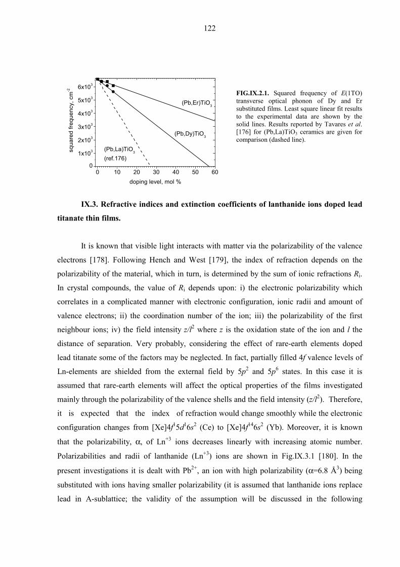
122
FIG.IX.2.1. Squared frequency of E(1TO) transverse optical phonon of Dy and Er substituted films. Least square linear fit results to the experimental data are shown by the solid lines. Results reported by Tavares et al. [176] for (Pb,La)TiO3 ceramics are given for comparison (dashed line).
IX.3. Refractive indices and extinction coefficients of lanthanide ions doped lead
titanate thin films.
It is known that visible light interacts with matter via the polarizability of the valence
electrons [178]. Following Hench and West [179], the index of refraction depends on the
polarizability of the material, which in turn, is determined by the sum of ionic refractions Ri.
In crystal compounds, the value of Ri depends upon: i) the electronic polarizability which
correlates in a complicated manner with electronic configuration, ionic radii and amount of
valence electrons; ii) the coordination number of the ion; iii) the polarizability of the first
neighbour ions; iv) the field intensity z/l2 where z is the oxidation state of the ion and l the
distance of separation. Very probably, considering the effect of rare-earth elements doped
lead titanate some of the factors may be neglected. In fact, partially filled 4f valence levels of
Ln-elements are shielded from the external field by 5p2 and 5p6 states. In this case it is
assumed that rare-earth elements will affect the optical properties of the films investigated
mainly through the polarizability of the valence shells and the field intensity (z/l2). Therefore,
it is expected that the index of refraction would change smoothly while the electronic
configuration changes from [Xe]4f15d16s2 (Ce) to [Xe]4f146s2 (Yb). Moreover, it is known
that the polarizability, α, of Ln+3 ions decreases linearly with increasing atomic number.
Polarizabilities and radii of lanthanide (Ln+3) ions are shown in Fig.IX.3.1 [180]. In the
present investigations it is dealt with Pb2+, an ion with high polarizability (α=6.8 Å3) being
substituted with ions having smaller polarizability (it is assumed that lanthanide ions replace
lead in A-sublattice; the validity of the assumption will be discussed in the following
0 10 20 30 40 50 600
1x10³
2x10³
3x10³
4x10³
5x10³
6x10³
(Pb,Dy)TiO3
squa
red
frequ
ency
, cm
-2
doping level, mol %
(Pb,La)TiO3 (ref.176)
(Pb,Er)TiO3

123
paragraphs). The dielectric constant of crystals can be expressed in terms of polarizability of
its constituent ions [180], αI, through:
( ) ( )0 01 / / 1 /i i i iN Nε α ε γ α ε = + Σ − Σ (IX.3.1)
where Ni is the number of atoms of species i per unit volume and γ is the Lorentz factor. In the
optical frequency range, the dielectric constant is equal to the squared index of refraction
FIG.IX.3.1. Radii and polarizabilities for +3 rare-earth ions, plotted vs. atomic number [180]
(n2=ε). Therefore, it is reasonable to expect a decrease in the refractive index of lanthanide
ions doped films with increasing dopant atomic number. This assumption is to some extent
consistent with the experimental results presented in paragraph VIII.3. The particular
behaviour of Ce doped films (Fig.VIII.3.1(a)) requires, however, some additional discussion.
A possible explanation of such behaviour can be proposed from the point of view of specific
oxidized state of Ce. It is well known that unlike the usual +3 oxidation state, peculiar to the
elements of Ln-series, Ce may also appear in the oxidation state +4. To our knowledge, the
experimental investigation of the oxidation state of Ce in Ce-substituted lead titanate thin
films is still lacking. In the present work, Ce doped PbTiO3 film is investigated by means of
X-ray Photoelectron Spectroscopy (XPS) since the position of XPS peaks is sensitive to
oxidized states of ions via peak position shifts. Fig.VIII.3.3(a) shows XPS spectra of PbTiO3
thin film doped with 5 mol % of Ce. The dashed line represents the spectra taken for as-
deposited film. The XPS spectra of the same sample measured after Ar ion cleaning at 1 keV,
70 nA for 2 min is shown by solid line. The Ar ion cleaning has not produced noticeable
modification of the spectra. Only the 1s peak of C, attributed to surface contamination,
disappeared. The detailed structure of the peak designated Ce 3d5/2 is shown separately in

124
Fig.VIII.3.3(b). The values of binding energy obtained by Gaussian fitting (881 and 877 eV)
indicate the presence of Ce in +4 oxidation state [181]. As discussed by Majumder et al.,
[129], it is very probable to find Ce in both +4 and +3 oxidation states in the case of PZT thin
films. Thus Ce ions can be distributed between A- and B-sites of the perovskite lattice: Ce3+
substitutes lead and imparts donor-type properties to the host material while Ce4+ substitutes
titanium due to smaller ionic radius and acts as isovalent impurity. However, the XPS peaks
corresponding to 4+ oxidation state of Ce may also arise from surface and grain boundary
segregation of CeO2, and XPS induced modification of Ce oxidation state have been also
considered [124]. Although these considerations make an interpretation of the XPS results
difficult, the optical and leakage current properties (the latter will be discussed in the
following) rather militate in favour of the presence Ce ions in Ce3+ and Ce4+ oxidation states,
and being distributed between A and B sublattices, respectively.
IX.4. Room temperature dielectric properties of pure and doped lead titanate
thin films.
The results of the room temperature dielectric characterization (paragraph VIII.4.) can
be discussed from the point of view of doping effects on domain wall mobility. It is well
known that the dielectric properties of ferroelectric materials are mainly determined by
domain wall oscillation under applied AC signal and oscillating domain walls are responsible
for unusually high dielectric constant peculiar to ferroelectric materials below their Curie
temperature. It was shown [182,183] that dielectric constant ε′ of ferroelectric thin film can be
expressed in terms of Rayleigh equation as:
' R IR Eε ε ε= + (IX.4.1)
where εR and εIR are reversible and irreversible Rayleigh parameters, respectively and E is
weak alternating electric field (smaller than Ec). Here the εR term is due to reversible domain
walls oscillation around some equilibrium position while the term EεIR is responsible for
irreversible domain walls movement.
As already discussed, doping with donor elements is compensated by cation vacancies
in order to preserve electroneutrality. Donor-cation vacancy combinations are thought to be
stable and so not to impede domain wall motion. Furthermore, donor doping compensates for
the p-type conductivity inherent to lead containing perovskites through the reduction of
oxygen vacancies, and this leads to higher domain wall mobility. Donor elements doped
perovskite ferroelectric materials are therefore known to have higher permittivity and loss

125
tangent than non-doped materials, and the results obtained in the present work (Fig.VIII.4.1)
are well in this trend. The increase of the dielectric constants and loss tangents of doped
specimens with respect to pure PbTiO3 can thus be explained in terms of contribution of
domain walls oscillation to the small signal dielectric properties, and the observed dependence
of ε′ and tanδ on the atomic number of doping element is opaque.
The decrease in ε′ and tanδ for doping levels higher than 5 mol % (Fig.VIII.4.2) may
be explained in terms of the appearance (in the case of Er doping) of second pyrochlore phase,
which is non-ferroelectric, or (in the case of Sm doping) to segregation effects/formation of
second phases at grain boundaries and/or film surface which may act as pinning centres.
IX.5. Effect of lanthanide ions doping on the ferroelectric-paraelectric phase
transition temperature.
A. Pure PbTiO3.
The dielectric constant and ferroelectric phase transition temperature of ferroelectric
thin films are influenced by many factors. First of all, solvent evaporation during thin film
deposition and difference in thermal expansion coefficients of the film and substrate can cause
the development of stress in the films [97,98]. Value and sign of stress are strongly dependent
on thin film deposition condition and type of substrate. Si has rather low value of thermal
expansion coefficient (CTE(Si)=2.6·10-1 °C-1). In turn, thermal expansion properties of lead
titanate are very sensitive to the temperature and may vary in wide range (Fig.IX.5.1 [185])
due to presence of structural phase transition. It is widely accepted in the literature
[97,98,118] that using Si as the substrate material mainly causes the development of tensile
biaxial stress in the ferroelectric film (Pt bottom electrode does not make significant
contribution into the resulting stress due to very small thickness (100-150 nm)). Depending on
the type of stress, the Curie point can be lowered or increased. In comparison to “stress-free”
ferroelectrics, it was predicted that two-dimensional compressive stresses oriented orthogonal
to the c polar axis result in an increase in the Curie point, while three-dimensional
(hydrostatic) compressive stresses lead to a decrease in the Curie temperature [119]. While
two-dimensional stresses can be developed due to difference in the thermal expansion
coefficients of the film and the substrate materials, in nano-sized structures, however,
compressive hydrostatic stresses can appear during cooling through the Curie temperature
owing to the clamping of the individual grain by neighbouring grains. The stress cannot be
relaxed by the 90° domain formation probably because of the monodomain state of the grains

126
[165,184] or the preponderance of 180° domains. Another factor affecting Curie transition
temperature of the films is grain size. In particular, Shaw et al. [115] showed that (Ba,Sr)TiO3
(BST) thin films deposited on Si substrates undergo ferroelectric-to-paraelectric phase
transition at lower temperature in comparison to BST ceramics. Chattopadhyay et al. [121]
investigated phase transition in nanocrystalline PbTiO3 by dielectric measurements, variable
temperature X-ray diffractometry and differential scanning calorimetry (DSC). The same
effect (lowering of Curie temperature with decreasing particle size) was observed. A
pronounced effect was revealed when the particle size was below 100 nm. The results of the
present work show that the curie transition temperature of pure lead-titanate thin films is
much lower that that reported for lead-titanate ceramics (450°C for PbTiO3 thin film in
comparison to 490°C of PbTiO3 ceramics [8]). This result can be explained both in terms of
stress state and grain size effects (see Fig.VII.1.6 and Table VII.1.1). The results described
above show that the mean grain size of lead titanate is approximately 100-140 nm. Therefore
it is straightforward to suppose that resulting stress in ferroelectric thin films depends in a
complicated manner on structural properties of the films (grain size, preferred orientation),
film thickness and deposition conditions.
FIG.IX.5.1. Temperature dependence of thermal expansion of lead titanate ceramics [185].
B. Ln-doped PbTiO3.
The Curie transition temperature, TC, was found to depend on the atomic number of
the Ln elements, i.e. on the ionic radius. The results show (Fig’s VIII.5.2, VIII.5.3 and Table
VIII.5.1) that TC decreases with the atomic number of Ln and concentration which suggest
that Ln-doping leads to the weakening of the ferroelectric order (in this regard the data of
dielectric measurements agree with the results of structural and Raman characterization), e.g.
by decreasing in the tetragonal distortion of the lattice (c/a) (see also Fig. VIII.1.3).
In the previous discussion the lanthanide ions were supposed to replace lead in A-
sublattice. In fact, The distribution of Ln-elements between A and B sites in the perovskite

127
lattice is subject of controversy. The results of dielectric characterization presented here are to
some extent in contradiction to those reported by Tan et al. [122] and Park et al. [125] on Ln-
doped PZT ceramics, where TC was found to increase with decreasing ionic radius of
lanthanides in comparison to undoped PZT (Fig.V.7.1). They explained their results in terms
of the site occupancy of Ln-ions being changed from A to B with decreasing ionic radius of
doping ion. The results of the dielectric characterization, obtained in the present work rather
suggest A-site substitution by the elements of Ln-series, although further experiments with
rare-earth doped PbTiO3 ceramics and volume cell calculation are required. Additionally, it
can be seen that the Curie point found for doped films does not correlate in a simple manner
with the grain size (as expected considering the results reported in [115,121], see above). In
fact, TC was found to decrease continuously for all concentrations investigated, although the
8% Er doped film shows a mean grain size similar to that of the undoped film (Table VII.1.1).
Therefore we speculate that the Curie temperature of our specimens is mainly controlled by
doping level and that the effect of grain size, in the range of grain sizes obtained, can be
neglected.
IX.6. Ferroelectric properties of PbTiO3 thin films doped with the elements of
lanthanide series.
The effects of doping on the P-E characteristics of PbTiO3 thin films have been
described in paragraph VIII.6. Ce, Sm, Dy and Er improve to some extent the shape of
hysteresis loops. This demonstrates that lanthanide elements doping leads to reduced DC
conductivity of the films especially at higher values of applied field (up to 400 kV/cm, see
Fig.VIII.6.1). With respect to technological applications of the films such effect (lowering of
conductivity) is rather advantageous because high DC conductivity peculiar to undoped lead
titanate complicates poling and increases the risk of break-down. Furthermore, as depicted
above, the ferroelectric parameters (remnant polarization and coercive field) correlate, to
some extent, with doping level. The data summarized in Tables VIII.6.1 and VIII.6.2 show
that with increasing doping level (case of Sm, Dy and Er substituted films) the ferroelectric
hysteresis loops become slimmer. The results can be explained in terms of the tetragonality
factor modification by doping. As shown above (Fig.VIII.1.3), doping with lanthanide ions
results in a significant lowering of c/a factor that is accompanied by the reduction of the
resulting dipole moment of the lattice. This can explain the decrease of remnant polarization
observed for doped films. Values of remnant polarization obtained for films doped with 5 and

128
8 mol % of Ln can be considered as the most reliable since contribution of DC conductivity in
P-E characteristics is minimized for these specimens.
The results of ferroelectric testing obtained for PET5 thin films deposited on LNO
electrodes (Fig.VIII.6.2) agree in general with the results reported by other groups for lead
based perovskite thin films of various compositions. Chen et al. [112] investigated the effect
of top and bottom electrode materials on the ferroelectric and fatigue properties of lead
zirconate titanate thin films. It is reported that while films deposited on LNO/Pt hybrid
electrodes are characterized by higher fatigue resistance, compared to those fabricated on Pt
electrode, the latter are reported to have higher values of the remnant polarization. Similar
effect of LNO buffer layer between film and Pt bottom electrode was demonstrated by Es-
Souni et al. [106] for sol-gel fabricated PLZT films with various La contents. It is supposed
by many authors (see paragraph V.5 and references therein) that the ferroelectric properties of
polycrystalline ferroelectric thin films are to a great extent determined by their morphologies
which, in turn, are affected by the substrate structure. However, the results of AFM
characterization reported in the present work unambiguously demonstrate that the
microstructure of the films of the same composition (PET5) was not crucially affected by the
type of bottom electrode (compare Fig’s VII.1.6(c) and (h)). Further investigations are
required in order to understand the mechanisms responsible for the deterioration of
ferroelectric properties of the films fabricated on LNO bottom electrode material.
IX.7. Thickness- and field-dependent dielectric properties of pure and doped lead
titanate thin films.
A. Dimensional effects on capacitance.
Reciprocal capacitance of PET5 thin films of different thickness deposited on Pt and
LNO bottom electrodes is plotted vs. film thickness in Fig.VIII.7.1. Agreement with the
proposed two-layers model can be noted for PET5 thin films deposited on LNO buffer layer.
The value of the interfacial capacity was determined for this set of specimens as 26.4 nF from
the intercept with the capacity axis. If we assume the thickness of the interfacial layer to be
about 10 nm, the dielectric constant of this layer is then about 10 (calculated using (VIII.4.1).
Apparent dielectric constant (bulk value) of the films deposited on LNO bottom electrode was
found from the slope of C-1 vs. d (Fig.VIII.7.1) as 294. This value is higher than those
calculated from the measured capacitances using (VIII.4.1): 251, 276 and 273 for the films of
thickness 195 nm, 260 nm and 390 nm, respectively. Comparison of measured values of

129
dielectric constant with the apparent one clearly demonstrates the deteriorative role of the
film-electrode interfacial layer.
At the same time, we must note that the thickness dependence of the reciprocal
capacity of the thin films deposited onto platinized Si substrate deviates from the linear
behaviour, and rather shows a parabolic dependence. These results imply that the Pt/PET5/Pt/
structure can not be treated as two capacitors connected in series. We speculate that besides
the interfacial layer formation, the thickness dependence of the thin film capacitance is
determined by the stress state (which is also thickness dependent and relaxes with increasing
d) developed during film crystallization. The stress is considered to relax in the films
deposited on LNO/Pt electrode probably due to the perovskite structure of LNO, in agreement
with the result reported in [113] while in Pt/PET5/Pt structure it remains almost unchanged. It
must also be noted that the parabolic behaviour of C-1(d) was found only for lead titanate thin
films, where the stress is particularly high due to relatively high room temperature
tetragonality factor. A linear C-1(d) dependence was reported for Er doped tetragonal PZT
[95].
B. C-V characteristics.
The voltage-dependent dielectric properties were investigated systematically with
regard to doping and bottom electrode material effects. Fig’s VIII.8.1 and VIII.8.2 exemplify
the room temperature ε′-E curves measured for films substituted with various amounts of Sm
and Er. The experimental results depicted above show the asymmetrical behaviour with
respect to both ε′ and E axes. The data demonstrate the presence of built-in fields in the films
investigated which are found to correlate with the type of dopant and doping level. Values of
built-in field, Eb and contribution of domain walls, η, to the measured dielectric constant were
obtained from the experimental ε′-E data and plotted in Fig. VIII.8.3 vs. doping level. The
increase of the contribution of domain walls to the dielectric response found for Sm
substituted films is in consistence with the concept of enhanced domain wall mobility in
donor ions doped materials [6,8]. Contrary to Sm, Er doping did not produce a significant
effect on η. The specific properties of Er doped films can be attributed to the role of
secondary phases (such as pyrochlore) in domain wall pinning processes. In fact, particles of
residual second phases can be considered as effective pinning centres for domain walls. The
existence of such particles is demonstrated using XRD analysis which revealed an enhanced
tendency to stabilize the pyrochlore phase for films doped with lanthanide of smaller ionic
radii (Dy and Er).

130
We must note further, that the value of EB correlates with the amount of lanthanide
ions added. Asymmetry of capacitance-voltage characteristics was extensively discussed by
Vorotilov et al. [103]. It was suggested that asymmetry of C-V curve and presence of the
built-in field originate from a disturbed layer near the bottom electrode-film interface. This
layer is characterized by a high density of point defects which serve as effective trap centers
for charge carriers, causing non-uniform distribution of net charge density through film
thickness (presence of the disturbed layer was also inferred from thickness dependent
capacitance of our specimens). Although the explanation of C-V curves asymmetry is
plausible, it does not explain the effects of doping on the value of built-in field. Internal bias
field formation in bulk ferroelectrics have been investigated by many groups (see references
[186-188]). Takahashi [186] discussed the effects of various (donor and acceptor) additives on
the internal bias in lead zirconate ceramics. It was demonstrated that acceptor-type doping
strengthens the internal bias while the opposite tendency was revealed for donor doped
materials. It was suggested that acceptor impurity-oxygen vacancy defect dipoles are
responsible for this phenomena. Arlt and Neumann [187] analysed quantitatively the
interplaying between bias field and defect dipoles in Ni-doped (up to 1%) BaTiO3. Based on
calculation of dipole energies they conclude that while in the paraelectric phase all three
directions are equivalent, below the Curie point acceptor ion-oxygen vacancy dipoles are
inclined to be oriented along the polarization direction. Warren et al. [188] investigated
processes of defect-dipole alignment in various ceramic materials by means of electron
paramagnetic resonance (EPR). In agreement with earlier work of Arlt and Neumann [187], it
was shown that alignment of defect-dipole complexes is possible only in tetragonal lattices.
Alignment was not observed in non-ferroelectric SrTiO3 and in Pb(Zr,Ti)O3 and BaTiO3
above their Curie temperatures.
The results of the present work show that with increasing Sm content the built-in field
vanishes. Three possible mechanisms can be proposed to explain this result: i) as discussed by
Arlt and Neumann [187] and Warren et al. [188], oxygen vacancies are involved in defect-
dipole complexes, and, due to the fact that they are considered as the most mobile defects in
perovskite lattices, are responsible for dipole reorientation processes. At the same time, donor
doping is known to reduce the concentration of oxygen vacancies. Therefore, it is expected to
observe the reduction of EB in donor impurities modified ceramic materials. The results
presented here are in agreement with this mechanism and with the data reported by Takahashi
[186]; ii) it was also demonstrated that alignment of defect complexes occurs along the c-axis
of the tetragonal lattice [187,188]. Due to the fact that doping with lanthanide ions leads to a

131
noticeable decrease in the tetragonal strain (Fig.VIII.1.3), it is straightforward to suppose that
the reduction in the built-in field is a consequence of the decrease of the role of lattice
tetragonality as a "driving force" for defect-dipole alignment processes.
As shown above, the ε′-E characteristics were significantly affected by the nature of
bottom electrode. The LNO bottom electrode leads to lower values of dielectric constant
(compared to films on Pt) and broadening of the peaks near the coercive field. This result
indicate that in the case of the film deposited on LNO electrode, the polarization switching
process is significantly hampered either by pinning centres which may arise from film-
electrode reaction layers or from the drop in the electric field at the low permittivity
interfacial layer (see above) .
IX.8. Voltage-, temperature- and thickness-dependent leakage currents in pure
and doped lead titanate thin films.
The J-E curves measured at various temperatures for PbTiO3 thin film deposited on
platinized silicon substrate are shown in Fig.VIII.9.1. The rectifying nature of Pt-PbTiO3
FIG.IX.8.1. Representation of leakage current data, obtained for non-doped lead titanate thin film (corresponding to Fig.VIII.9.1) in full logarithmic form (a – negative and c – positive parts) and vs. square root of applied bias field (b - negative and d – positive parts). Absolute values of field and current are taken.
10 10010-1010-910-810-710-610-510-410-310-210-1100
2.82
J, A
/cm
2
E, kV/cm
40°C 60°C 120°C
(a)3.65
0 2 4 6 8 10 12 14 1610-1010-910-810-710-610-510-410-310-210-1100
40°C 60°C 120°C
J, A
/cm
2
E1/2, (kV/cm)1/2
(b)
10 100
10-8
10-7
10-6
10-5
10-4
10-3 2.16 3.63
4.85
1.51
0.81
40°C 60°C 120°C
J, A
/cm
2
E, kV/cm
0.42 (c)
0 2 4 6 8 10 12 14 16
10-8
10-7
10-6
10-5
10-4
10-3
(d)
40°C 60°C 120°C
J, A
/cm
2
E1/2, (kV/cm)1/2

132
FIG.IX.8.2. Leakage current density in non-doped lead titanate thin film of thickness 267 nm (negative potential is applied to the bottom electrode) selected for different field and plotted in Schottky (a) and Poole-Frenkel (b) coordinates.
contact indicates the presence of Schottky-type barrier (see paragraph V.8 and ref 139). The
weakening of rectifying ability of the contact at elevated temperature can be explained by
barrier lowering (will be analyzed in the following).
Schottky type emission (interface limited) and SCLC (bulk limited) mechanisms (see
paragraph V.8 and references therein) were claimed by many research groups as the operating
conduction processes in ferroelectric thin films. Conclusions about the conduction mechanism
prevailing under certain conditions (temperature and DC bias voltage) are usually done based
on the analysis of the shape and the character of J-E dependences. In case of Schottky
mechanism linear plots of logJ vs. E1/2 should be obtained (see equation (V.8.8)). The SCLC
mechanism should lead to linear logJ-logE plots (see equation (V.8.11)). Fig.IX.8.1
represents the leakage current data, obtained for non-doped lead titanate thin films
(corresponding to Fig.VIII.9.1) as double logarithmic plots (a – negative and c – positive
parts), and as log J vs. E1/2 (b - negative and d – positive parts). It can be seen that the
negative side of logJ-logE plots (a) can be linearly fitted with decreased slope for data
acquired at higher temperatures. With increasing temperature (see data for 120°C) deviation
from linear behaviour is observed. The logJ-E1/2 plot (b) shows a linear behaviour at higher
fields (higher than 50 kV/cm) and a more complex behaviour at lower values of the bias
fields. An even more complex J-E dependence is revealed for the case when positive potential
was applied to the bottom electrode (forward biased metal-dielectric contact, Fig's IX.8.1(c)
and,(d)). logJ-logE plots (c) can be divided in three regions. The low field part shows a linear
dependence with increasing slope as the temperature increases. Such behaviour and the values
2.4 2.6 2.8 3.0 3.2 3.4
10-12
10-11
10-10
10-9
10-8
φE, eV
0.040.06
0.10
0.17
0.240.29
202.25149.81
97.38
52.4329.9622.46
J/
T2 , A/(c
m.K
)2
1000/T, 1/K
14.98
E, kV/cm
0.39(a)2.4 2.6 2.8 3.0 3.2 3.4
10-8
10-7
10-6
10-5
0.44
0.100.12
0.16
0.23
0.300.35
J/E,
A/(c
m.k
V)
1000/T, 1/K
202.25149.8197.3852.4329.9622.4614.98
E, kV/cm
φE, eV
(b)

133
of slope (in the vicinity of unit) let us treat the metal-ferroelectric-metal contact as ohmic in
the range of the field under consideration. Another linear region on logJ-logE plots can be
recognized at high field (higher than 150 kV/cm). This region is characterized by a slope
which is found to decrease when the temperature increases. Similar observations on PZT thin
film were attributed by Shin et al. [96] to the onset of the SCLC mechanism. Overlapping of
several conducting mechanisms may be responsible for more complex logJ-logE dependences
in the intermediate field range. The positive part of the J-E curve plotted in logJ-E1/2 form
(Fig. VIII.8.1(d)) reveals that the linear behaviour can be observed only in the high field
region. Thus, it can be seen that in the case of non-doped PbTiO3 thin film it is very difficult
to state which mechanism is responsible for the conduction in the field and temperature
ranges investigated. Fig.IX.8.2 shows leakage current densities of non-doped lead titanate thin films
selected for different fields and plotted in Schottky (a) and Poole-Frenkel (b) coordinates.
Irrespective of the mechanism supposed, temperature and field activated processes are
observed. It is important to note that the slopes of the plots decrease with increasing applied
bias field indicating field induced barrier lowering. The barrier height, measured at fixed
applied bias and found from logJ/T2-1/T or logJ/E-1/T plots is designated φE (eV). It is
obvious from equations (V.8.8) and (V.8.9) that ( / 4 )B B iq qEφ φ πε= − − (Schottky)
and ( / )B B iq qEφ φ πε= − − (Poole-Frenkel) and that φE vs. E1/2 plot must yield straight lines.
Contrary to what is expected, φE shows rather complex behaviour for both Schottky and
Poole-Frenkel models with respect to E1/2, as illustrated in Fig.IX.8.3. It means that the data of
leakage currents acquired for the non-doped lead titanate thin film arise from the
superposition of many processes, and that conduction is controlled by different mechanisms
operating simultaneously in the high field region.
FIG.IX.8.3. Field-dependent barrier height for non-doped PbTiO3 thin film.
4 6 8 10 12 14 160.0
0.1
0.2
0.3
0.4
Schottky Poole-Frenkel
φ E, e
V
E1/2, (kV/cm)2

134
Doping with either donor or acceptor elements can stabilize the defect structure of the
thin films and compensate the influence of unintentional and uncontrollable impurities on the
electrical properties of the ferroelectric capacitor [131]. The results of the present work show
that, additionally to a noticeable decrease of leakage current density (Fig'sVIII.9.2), doping
with donor elements also affects the character of φE-E1/2 dependence. The most reliable results
were obtained for Sm substituted films because Sm modifies phase content of the films to the
least extent. The values of field-dependent barrier height calculated for film, substituted with
2 mol % of Sm are represented in Fig.IX.8.4. The data plotted in φE-E1/2 form can be well
fitted with a straight lines and zero-field barrier height φB can be obtained from the intercept
with the ordinate axis. Considering Schottky and Poole-Frenkel models, values of φB were
determined as 1.52 eV and 1.61 eV, respectively. Barrier height φB=0.8 eV (assuming
Schottky model) was reported for sol-gel PZT films having Pt top and bottom electrodes by
Stolichnov and Tagantsev [134]. The value was obtained at the field of 250 kV/cm and zero-
field barrier height was not reported for those specimens. Extrapolation of our results
(Fig.IX.8.4) to E1/2=15.81 (kV/cm)1/2 (2501/2=15.81 (kV/cm)1/2) gives the value of Schottky
barrier of approximately 0.4 eV which is two time less than reported in [134]. Blom et al.
[133] give the barrier height of 2 eV for Au-PbTiO3 (PLD) contact. The value was deduced
from metal-ferroelectric band structure consideration assuming ferroelectric to be of p-type.
Taking into an account the fact, that Pt electrode has higher work function (5.7 eV) compared
to that of Au (5.2 eV) [139, p.251], barrier height of Pt-PbTiO3 structure might be even
higher. It is obviously that φB is very sensitive to factors determining the quality of metal-
ferroelectric interface such as deposition method, film composition and fabrication
parameters.
FIG.IX.8.4. Field-dependent barrier height for 2 mol % of Sm doped lead titanate thin films (d=245 nm).
6 8 10 12 14 160.4
0.5
0.6
0.7
0.8
0.9
1.0
1.1
φB=1.61 eV
Schottky Poole-Frenkel Linear fit
φ E, e
V
E1/2, (kV/cm)1/2
φB=1.52 eV
(b)

135
FIG.IX.8.5. Representation of leakage current data (negative part), obtained for PET5 thin film deposited on lanthanum nickel oxide bottom electrode (corresponding to Fig.VIII.9.3(a)) in full logarithmic form (a) and vs. square root of applied bias field (b). Absolute values of field and current are taken. Results of linear fit to the experimental data are represented by solid lines. Numbers indicate the slopes found for linear regions of the logJ-logE and logJ-E1/2 characteristics.
FIG.IX.8.6. Representation of leakage current data (negative part), obtained for PET5 thin film deposited on platinized substrate (corresponding to Fig.VIII.9.3(b)) in full logarithmic form (a) and vs. square root of applied bias field (b). Absolute values of field and current are taken. Results of linear fit to the experimental data are represented by solid lines. Numbers indicate the slopes found for linear regions of the logJ-logE and logJ-E1/2 characteristics.
The negative parts of the J-E characteristics obtained at various temperatures for the
film fabricated on LNO and Pt bottom electrodes (corresponding to Fig's VIII.9.3(a) and (b))
are illustrated in Fig's IX.8.5 and IX.8.6, respectively, in full logarithmic (a) and logJ-E1/2 (b)
forms. Data obtained for PET5/LNO/Pt structure (Fig VIII.9.3.(a)) and presented in the log-
log plot (Fig.IX.8.5(a)) can be well fitted with straight lines in the range of temperature and
DC bias field investigated with nearly constant slope, while a more complex dependence of
10 10010-9
10-8
10-7
10-6
10-5
10-4
10-3 40°C 60°C 80°C 100°C
2.46
2.63
J, A
/cm
2
E, kV/cm
2.52 (a)
2 4 6 8 10 12 14 16 18 20 2210-8
10-7
10-6
10-5
10-4
10-3 40°C 60°C 100°C 120°C
J, A
/cm
2
E1/2, (kV/cm)1/2
(b)
10 100
10-9
10-8
10-7
10-6
10-5
10-4
10-3 40°C 60°C 80°C 100°C
J, A
/cm
2
E, kV/cm
(a)
0 2 4 6 8 10 12 14 16
10-9
10-8
10-7
10-6
10-5
10-4
10-3
40°C 60°C 80°C 100°C
J, A
/cm
2
E1/2, (kV/cm)1/2
(b)
0.330.34

136
logJ vs. E1/2 is found (Fig.IX.8.5(b)) for this structure. The data represented for PET5 films
deposited on Pt electrode can be well fitted to Schottky model at lower temperature
(Fig.IX.8.6(b)) (Schottky and Poole-Frenkel models yield zero-field barrier height 0.53 eV
and 0.6 eV, respectively) and demonstrate a more complex behaviour at elevated
temperatures. We suppose that in the films fabricated on LNO bottom electrodes, the
conductivity processes are mainly operated by the SCLC mechanism in the ranges of
temperatures and fields investigated, whereas interface-limited Schottky mechanism is
responsible for conductivity in the films fabricated on platinized Si substrates at lower
temperature (in agreement with earlier papers, see references sited in paragraph V.8). At
higher temperatures (100-120°C) the presence of both Schottky and SCLC mechanisms is
supposed. Investigations of the leakage current density as a function of thickness of our
samples (Fig.VIII.9.4) confirm this supposition. The dependence of leakage current density on
film thickness was found to be more pronounced for specimens deposited on LNO electrode.
For a set of specimens fabricated on Pt bottom electrode, the leakage current density was
found to be practically thickness independent at lower temperature (slope m is less than unit).

137
X. Choice of application: doped PbTiO3 thin films for pyroelectric and piezoelectric detectors
A. Results of pyroelectric and piezoelectric measurements.
The pyroelectric and piezoelectric properties were determined exemplary for PbTiO3
films substituted with 5 mol % of Sm and Er. The thin films consisted of 12 layers (see
paragraph VII.1 for the details on specimen preparation). For the pyroelectric coefficient
determination, the specimen temperature was sinusoidally varied in the frequency range from
0.03 to 0.2 Hz using a thermoelectric element (Peltier element) operated with a function
generator. The temperature of the specimen was controlled via the measurements of the top
electrode resistance (bolometric effect). Two diagonal contacts of the electrode structure
illustrated in Fig. VII.1.7 were used. The electrode was calibrated prior to the experiment
using commercial thermal sensor placed on the sample surface. Fig.X.1 exemplifies
temperature dependence of Pt top electrode resistance. Peak values of the resistance and
temperature were used to obtain calibration coefficient. The pyroelectric current measured
with a digital lock-in amplifier was used to calculate the pyroelectric coefficient of the
specimens (see paragraph VII.2 for more details). The values of the pyroelectric coefficients
are found to be 63 µC/m2K and 122 µC/m2K for as-prepared (unpoled) PST5 and PET5 thin
films, respectively.
FIG.X.1. Data used for Pt top electrode calibration: dependence of electrode resistance on the temperature of the specimen surface.
156.2
156.3
156.4
156.5
156.6
156.7
156.8
19
20
21
22
23
Elec
trode
resi
stan
ce, O
hm
Time, arb. units.
resistance temperature
Sur
face
tem
pera
ture
, °C

138
FIG.X.2. Surface temperature variation and pyrodynamic response (pyroelectric current density) measured for unpoled PST5 (a) and PET5 (b) thin films. Background level is also presented for comparison (c). Thermal cycling was done at a frequency of 0.01 Hz using the Peltier element.
20.5
21.0
21.5
22.0
22.5
23.0
23.5
24.0
-80
-60
-40
-20
0
20
40
60
80 sample temperature
T, °
C
Time, arb. inits
(c) current density
J, n
A/cm
2
20.5
21.0
21.5
22.0
22.5
23.0
23.5
24.0
-800-600-400-2000200400600800
T, °C
Time, arb. units
sample temperature
(a) pyroelectric current density
J, n
A/cm
220.0
20.5
21.0
21.5
22.0
22.5
23.0
-3000
-2000
-1000
0
1000
2000
3000
T, °C
Time, arb. units
sample temperature
(b)J,
nA/
cm2
pyroelectric current density
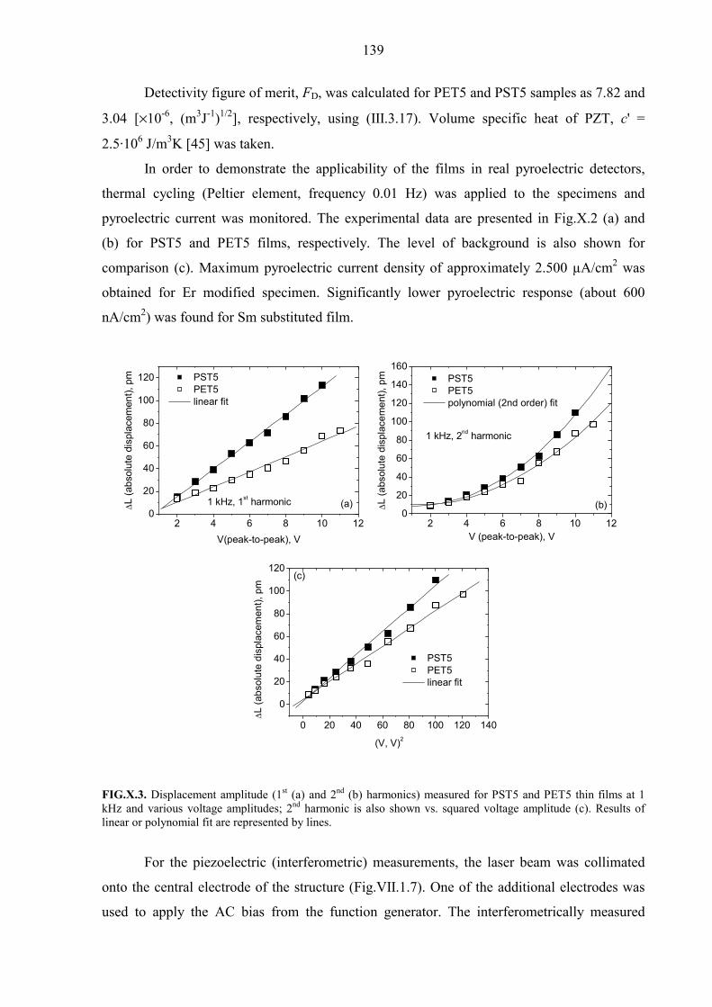
139
Detectivity figure of merit, FD, was calculated for PET5 and PST5 samples as 7.82 and
3.04 [×10-6, (m3J-1)1/2], respectively, using (III.3.17). Volume specific heat of PZT, c' =
2.5·106 J/m3K [45] was taken.
In order to demonstrate the applicability of the films in real pyroelectric detectors,
thermal cycling (Peltier element, frequency 0.01 Hz) was applied to the specimens and
pyroelectric current was monitored. The experimental data are presented in Fig.X.2 (a) and
(b) for PST5 and PET5 films, respectively. The level of background is also shown for
comparison (c). Maximum pyroelectric current density of approximately 2.500 µA/cm2 was
obtained for Er modified specimen. Significantly lower pyroelectric response (about 600
nA/cm2) was found for Sm substituted film.
FIG.X.3. Displacement amplitude (1st (a) and 2nd (b) harmonics) measured for PST5 and PET5 thin films at 1 kHz and various voltage amplitudes; 2nd harmonic is also shown vs. squared voltage amplitude (c). Results of linear or polynomial fit are represented by lines.
For the piezoelectric (interferometric) measurements, the laser beam was collimated
onto the central electrode of the structure (Fig.VII.1.7). One of the additional electrodes was
used to apply the AC bias from the function generator. The interferometrically measured
2 4 6 8 10 120
20
40
60
80
100
120
PST5 PET5 linear fit
∆L (a
bsol
ute
disp
lace
men
t), p
m
V(peak-to-peak), V
1 kHz, 1st harmonic (a)
2 4 6 8 10 120
20
40
60
80
100
120
140
160
PST5 PET5 polynomial (2nd order) fit
∆ L (a
bsol
ute
disp
lace
men
t), p
m
V (peak-to-peak), V
1 kHz, 2nd harmonic
(b)
0 20 40 60 80 100 120 140
0
20
40
60
80
100
120
PST5 PET5 linear fit
∆ L (a
bsol
ute
disp
lace
men
t), p
m
(V, V)2
(c)

140
piezoelectric response from the films investigated is presented in Fig.X.3 as function of
applied AC voltage amplitude (absolute value of sample surface displacement is shown). A
linear dependences of the displacement amplitude found for both specimens allows the field
independent effective piezoelectric coefficients, deff, to be obtained in the range of the fields
investigated (Fig.X.3(a), 1st harmonic). Fig's X.3 (b) and (c) show 2nd harmonic generated due
to electrostriction effect. ∆L plotted vs. squared voltage amplitude (Fig.X.3(c)) can be well
fitted to the straight line and electrostriction coefficients of the specimens to be found. The
results of the pyroelectric and piezoelectric characterization of selected specimens are
summarized in Table X.1. Room temperature dielectric properties (dielectric constant and loss
tangent) are also given.
Table X.1. Pyroelectric and piezoelectric properties of 5 mol % of Sm and Er substituted PbTiO3 thin films.
FIG.X.4. DC bias field-dependent piezoelectric response from Sm and Er substituted thin films.
Additionally, DC field-dependent piezoelectric response from the films was
investigated. For this purpose, DC voltage was applied across the capacitor of interest and
oscillation of the sample surface was excited by the application of an AC signal from the
function generator. Frequency and amplitude of the AC voltage were 1 kHz and 1Vp-p,
PST5 PET5 p, µC/m2K 63 122 deff, pm/V 48.4 26.8 meff×10-6, (cm/kV)2
4.308 3.292
ε′ (1 kHz) 310 220 tanδ (1 kHz) 0.025 0.02 FD×10-6, (m3J-1)1/2
3.04 7.82
-300 -200 -100 0 100 200 3000
20
40
60
80
100
120
PbTiO3+ 5 mol % Sm
PbTiO3+ 5 mol % Er
∆L (d
ispl
acem
ent a
mpl
itude
), pm
E, kV/cm
141
respectively. The DC bias amplitude was 25 V that corresponds to a field of approximately
260 kV/cm. The piezoelectric hysteresis loops obtained for PST5 and PET5 films are shown
in Fig.X.4. DC bias sweep starts at zero voltage. The directions of voltage change are
indicated by arrows in the figure. It can be seen that (similarly to ε′-E data, paragraph VIII.8)
maximum displacements are reached at DC biases corresponding to the coercive fields of the
films due to ferroelectric switching.
B. Discussions.
We must note first that unlike bulk ceramics, the pyroelectric and piezoelectric
responses were measured for the as-deposited (unpoled) specimens. The fact that despite
unpoling pyroelectric and piezoelectric responses were detected can be explained in terms of
self-polarization of the films, probably due to the stress developed during crystallization and
cooling through the Curie temperature. Self-polarized states of the films could be very useful
from the point of view of the potential applications in different integrated devices (IR imaging
devices, MEMS) where poling is difficult to achieve. Moreover, the self-polarized state in our
films is very stable, and poling did not produce a noticeable effect on the pyroelectric and
piezoelectric responses. It is known that in the PbZrO3-PbTiO3 system of solid solutions, the
effect of poling is maximum for compositions close to the MPB (corresponds to PZT (52/48))
whereas in Ti-rich compounds (especially in PbTiO3) it is marginal. In this respect, the results
presented here agree with early published data ([44] and Table III.3.1).
The nature of the doping element affects the value of the pyroelectric coefficient.
Doping with 5 mol % of Er increases substantially the pyroelectric coefficient (compared to 5
mol % of Sm substituted film). The explanation to this result can be given in terms of the
effect of doping on the preferred orientation of the crystallites. As already discussed, the films
doped with Er are characterized by a pronounced (100) out-of-plane fibre texture (see
paragraph VIII.1) whereas for Sm doped films [100] axis of the fibre texture was found to
form an angle of approximately 54° with the normal to the sample plane (Fig's VIII.1.4 and
VIII.1.5). Obviously, higher pyroelectric coefficients are expected for films containing larger
amount of domains/grains aligned with their polar axis perpendicular to the plane of the
specimen. The (100)-out-of-plane preferentially oriented Er doped films are abundant in the
grains which can be polarized in the perpendicular (to the specimen plane) direction. Roughly
(neglecting the effect of ionic radius on the lattice tetragonality and hence on the value of the
spontaneous polarization), p(PST5) shall be equal to p(PET5)cos54°. The experimental results
obtained (Table X.1) are in general agreement with this assumption. These results

142
unambiguously show the decisive influence of preferred orientations on the pyroelectric
response of unpoled sol-gel fabricated PbTiO3 thin films. Furthermore, it is known that the
maximum of the pyroelectric coefficient of ferroelectric materials lies in the vicinity of their
Curie point, and the reduction of the Curie temperature therefore can cause some increase in
the pyroelectric coefficient. The temperature dependent dielectric properties of lanthanide
doped PbTiO3 thin films investigated above (see paragraph VIII.5) show that films substituted
with Er undergo ferroelectric-to-paraelectric phase transition at temperatures somewhat lower
than those of Sm substituted films. Therefore the results of pyroelectric characterization of
our films can also be explained in terms of the lanthanide doping on the Curie temperature of
the films.
The values of p measured for both specimens (Table X.1) are substantially lower than
those found for poled pyroelectric ceramics (p=380 µC/m2K, modified PZT ceramics [45] and
PT based thin films (p=250-1500 µC/m2K [44, Wersing and Bruchhaus, p.186]) deposited on
single crystalline MgO, LNO and sapphire substrates, but exceed those known for polymer
pyroelectric materials (p=27 µC/m2K, PVDF) [45]. However, it must be noted that in the case
of ferroelectric thin films, method of deposition, material of substrate and even technique
utilized for pyroelectric coefficient determination could play a decisive role and must be taken
into an account.
The results of piezoelectric characterization of PbTiO3 films modified with 5 mol % of
Sm and Er (Fig. X.3 and Table X.1) contradict the observations of Lefki and Dormans [189]
who reported the absence of piezoelectric activity for as-deposited (unpoled) sol-gel PZT
films. At the same time, the effective piezoelectric coefficients obtained for PST5 and PET5
thin films were by a factor of two higher than those reported by these authors for unpoled
OMCVD PZT films [189]. Piezoelectric coefficients of lead titanate thin films were not found
in the literature. The data are lacking probably due to difficulties in preparation and
piezoelectric properties characterization (due to high risk of cracking and conductivity of lead
titanate films) and high conductivity of undoped films. The first harmonic of the displacement
amplitude was found to be linear with respect to the amplitude of applied AC signal for both
specimens and piezoelectric coefficient deff is constant in the entire range of driving fields
investigated (from 0 to 11 Vp-p or from 0 to approximately 58 kV/cm field amplitude).
Apparently, the range of linearity of piezoelectric properties of our specimens is larger
compared to PZT thin films and ceramics of various compositions [190,191]. It is known that
both 180°- and 90°-domain walls contribute to the dielectric properties of tetragonal thin films
(extrinsic response) while only 90° domains are responsible for piezoelectric activity of the
143
films and ceramics [145,192] (neighbour 180°-domains displace in the antiparallel directions
compensating each other; in the case of 90°-domains this compensation does not occur). The
non-linear piezoelectric activity is attributed to domain contribution while the "linear portion"
of the field-dependent piezoelectric properties corresponds to the lattice contribution (intrinsic
contribution). The results of piezoelectric measurements (Fig.X.3(a)) suggest rather
monodomain state of the grains and/or preponderance of 180°-domains. It is useful to
consider the results of piezoelectric characterization together with those of ε′-E
measurements. In particular, Fig.VIII.8.3 compares the contribution of domains, η, to the
measured dielectric constant obtained for Sm and Er substituted films. One can see that
doping with Sm resulted in an increase of domain wall mobility or concentration while the
effect of Er can be neglected. Thereby, the increase of domain wall mobility and/or
concentration in Sm substituted films is confirmed only by means of dielectric
characterization. Therefore it is straightforward to suppose that doping with Sm rather creates
180°-domains while crystallites of Er substituted film remain in monodomain state.
Furthermore, we can see that doping with Sm results in a higher value of linear (field-
independent) deff compared to that of Er doped films. Increase of measured value of
piezoelectric coefficient (Table X.1) can be attributed to higher lattice (intrinsic) contribution
to the apparent piezoelectric response of Sm substituted film (in comparison to Er substituted
specimen).
In conclusion, as demonstrated for dielectric and pyroelectric properties, the
piezoelectric coefficient of PbTiO3 thin films can also be influenced, viz. tailored, by varying
the ionic radius/atomic number of doping lanthanides.
144
IX. Summary and conclusions
Structural, electrophysical and functional properties of lead titanate thin films
substituted with elements of the lanthanide series were systematically investigated and
discussed in this thesis. The sol-gel method was adopted for specimen preparation. Ce, Sm,
Dy, Er and Yb were chosen as doping elements. The experimental conditions were optimized
so as to allow deposition of crack-free thin films with homogeneous morphology. Various
characterization methods were used to investigate correlation between ionic radius,
concentration of doping ions and properties of the films. The structural properties (texture
and phase composition) of the specimens were investigated by means of X-ray diffractometry
and Raman spectroscopy. Low and high frequency (optical) dielectric, ferroelectric and
leakage properties were characterized as a function of temperature. Additionally, the effects
of the bottom electrode material and film thickness were investigated for a set of selected
specimens. In order to investigate the applicability of lanthanide ions substituted films in IR
and piezoelectric sensors, pyroelectric and effective piezoelectric coefficients of some
selected samples were measured and compared with those reported for thin films and
ceramics by other research groups. The results are discussed in terms of doping effects, the
combined effects of stress development, influence of the grain size and film thickness. Based
on the results of the present work the following conclusions can be drawn:
The optimized processing conditions lead to the crystallization of the
tetragonal perovskite phase. Very fine polycrystalline (grain size was found to
be in the range of 100-140 nm) homogeneous microstructures of the films were
obtained. Residual pyrochlore (paraelectric) was found to form thin
(presumably of approximately 10 nm thickness) layer in the near surface
region. The amount this phase increased with decreasing ionic radius of doping
ion (case of Dy and Er).
Θ-2Θ and grazing incidence XRD characterization of the films revealed the
decrease of lattice tetragonality for all doping elements investigated.

145
Pole figure and fibre texture plot analysis of the films deposited on (111)
textured Pt bottom electrode showed (100) out-of-plane texture for pure and
Dy and Er substituted films. Ce, Sm and Yb substituted films were found to be
characterized by (100)+(111) preferred orientation with no in-plane alignment.
Raman spectroscopy confirmed the tetragonal perovskite structure of the thin
films. The softening of the E(1TO) soft mode was found for pure and doped
films. The results were attributed to grain size effects and stress development
for the undoped film. Doping with rare-earth ions caused further decrease of
the soft phonon frequency indicating the decrease of the ferroelectric order in
the films. These results agree also with the observed decrease of Curie
transition temperature and lattice tetragonality of pure and doped films.
The effects of lanthanide ions substitution on the low and high (optical)
frequency dielectric properties of lead titanate thin films were systematically
investigated. It is shown that the index of refraction and the small signal
dielectric properties (dielectric constant and loss tangent) correlate not only
with doping level, but are also with the atomic number/ionic radius of dopant.
With the exception of Ce, the indices of refraction of the films are shown to
decrease with decreasing ionic radius of doping ion. The results are explained
in terms of substitution of lead with ions of smaller polarizability. The specific
behaviour of Ce is attributed to the 4+ oxidation state revealed by means of
XPS analysis. The Curie phase transition temperature of pure lead titanate thin
films was found to be lower than that of bulk ceramics and, on the other hand,
was found to correlate with the atomic number and concentration of dopant,
viz. TC decreases with increasing atomic number of doping element. TC was
also found to decrease with increasing doping level for all elements
investigated. Comparison of the results of electrical characterization reported
in the present work with those published by other research groups for thin
films and ceramics of various compositions enable us to suppose A-site
substitution (donor-type) for all Ln elements investigated.
Ferroelectric and field-dependent dielectric properties of doped specimens
were investigated with respect to bottom electrode material and type of doping
ions. Doping of lead titanate thin films fabricated on Pt electrode with Sm, Ce,
Dy and Er was found to improve the shape of the ferroelectric hysteresis loop
due to compensation of conductivity. The use of lanthanum nickel oxide

146
(LNO) as a bottom electrode material caused poor ferroelectric properties.
Analysis of ε′-E characteristics obtained for lanthanide elements doped films
revealed increased contribution of domain walls and their mobility in Sm
substituted films. Much smaller effect was found for Er-doped films.
Analysis of the results of leakage current properties characterizations shows
that conduction in the films fabricated on LNO bottom electrodes is mainly
operated by the space charge limited current (SCLC) mechanism in the ranges
of temperature and field investigated. Interface-limited Schottky mechanism is
found to be responsible for conductivity at lower temperature in the films
fabricated on platinized Si substrates. At higher temperatures (100-120°C) the
presence of both Schottky and SCLC mechanisms is supposed.
5 mol % of Sm and Er doped thin films demonstrated pyroelectric and
piezoelectric activity in the as-deposited (unpoled) state due to self-
polarization. The pyroelectric and piezoelectric properties of the films are
found to be sensitive to the ionic radius/atomic number of lanthanide ions. Sm
substituted films are characterized by better piezoelectric and poor pyroelectric
properties, while the reverse was found for Er substituted films.

147
List of references.
[1] J. Valasek, Phys. Rev. 15, 537 (1920).
[2] W. Känzig, Ferroelectrics, 74, 285 (1987).
[3] G. Busch, Ferroelectrics, 71, 43 (1987).
[4] J. Fousek, Ferroelectrics, 113, 3 (1991).
[5] G. Busch, Ferroelectrics, 74, 267 (1987).
[6] G.H. Haertling, J. Am. Ceram. Soc. 82, 797 (1999).
[7] C. Kittel, Introduction to Solid State Physics (John Wiley and Sons, New York, 1996)
pp.393-394.
[8] Y. Xu, Ferroelectric Materials and Their Applications (North-Holland, Amsterdam,
1991) p.3.
[9] A.F. Wells, Structural Inorganic Chemistry (Clarendon Press, Oxford, 1995), pp. 584-
588.
[10] S. Iakovlev, unpublished.
[11] A.F. Devonshire, Adv. Phys. 3, 85 (1954).
[12] C. Brennan, Integr. Ferroelectr. 8, 335 (1995).
[13] R. Blinc, B. Žekš, Soft Modes in Ferroelectrics and Antiferroelectrics (North-
Holland, Amsterdam, 1974) pp. 36-45.
[14] A. von Hippel et al., N.D.R.C. Rep. No. 300, August 1944, cited in Tech. Rep. 51
(1950) Massachusetts Institute of Technology.
[15] J.F. Scott, Ferroelectric Memories (Springer, Berlin, 2000) pp.79-94.
[16] Ferroelectric Thin Films: Synthesis and Basic Properties, ed. C.P. de Araujo, J.F.
Scott, G.W. Taylor (Gordon and Breach, Amsterdam, 1996).
[17] R.L. Sandstrom, W.J. Gallagner, T.R. Dinger, R.H. Koch, R.B. Laibowitz, A.W.
Kleinsasser, R.G. Gambino, B. Bumble, M.F. Chisholm, Appl. Phys. Lett. 53, 444
(1988).
[18] R.B. Laibowitz, R.H. Koch, P. Chaudari, R.J. Gambino, Phys. Rev. B, 35, 8821
(1987).

148
[19] D. Dijkkamp, T. Venkatesan, X.D. Wu, S.A. Shaheen, N. Jisrawi, Y.H. Min-Lee,
W.L. McLean, M. Croft, Appl. Phys. Lett. 51, 619 (1987).
[20] J. Narayan, N. Buinno, R. Singh, O.W. Holland, O. Auciello, Appl. Phys. Lett. 51,
1845 (1988).
[21] J.S. Horwitz, K.S. Grabowski, D.B. Chrisey, R.E. Leuchtner, Appl. Phys. Lett. 59,
1565 (1991).
[22] C.M. Cotell, K.S. Grabowski, MRS Bull. 17, 44 (1992).
[23] H.M. Manasevit, W.I. Simpson, J. Electrochem. Soc. 116, 1725 (1969).
[24] Sol-gel Technolohy for Thin Films, Fibers, Preforms, Electronics, and Specialty
Shapes, ed. L.C. Klein (Noyes Publications, Park Ridge, New Jersey, U.S.A.,
1988).
[25] K.D Budd, S.K. Dey, D.A. Payne, Brit. Ceram. Proc. 36, 107 (1985).
[26] B.A. Tuttle, R.W. Schwartz, MRS Bullet. 21, 49 (1996).
[27] Z. Kighelman, D. Damjanovic, A. Seifert, S. Gentil, S. Hiboux, N. Setter, Mater.
Res. Soc. Symp. Proc. 596, 523 (2000).
[28] J.-G. Cheng, J. Tang, X.-J. Meng, S.-L. Guo, J.-H. Chu, M. Wang, H. Wang, Z.
Wang, J. Amer. Ceram. Sos. 84, 1421 (2001).
[29] V. Joshi, D. Roy, M.L. Mecarthey, Appl. Phys. Lett. 63, 1331 (1993).
[30] A. Montenero, M. Canali, H. Gnappi, D. Bersani, P.P. Lottici, P. Nunziante, E.
Traversa, Appl. Organometal. Chem. 11, 137 (1997).
[31] A. Li, C. Ge, P. Lü, D. Wu, S. Xiong, N. Ming, Appl. Phys. Lett. 70, 1616 (1997).
[32] P.F. Baude, C. Ye, D.L. Polla, Mater. Res. Soc. Symp. Proc. 310, 139 (1993).
[33] D.L. Segal, J. Non-Crystalline Solids, 63, 183-191 (1984).
[34] A.C. Pierre, Introduction to Sol-Gel Processing (Kluwer Academic Publishers,
Boston, 1998) p. 4.
[35] C.J. Brinker, Sol-Gel Science: the Physics and Chemistry of Sol-Gel Processing
(Academic Press, London, 1990) p. 29.
[36] R.W. Schwartz, R.A. Assink, D. Dimos, M.B. Sinclair, T.J. Boyle, C.D. Buchheit,
Mater. Res. Soc. Symp. Proc. 361, 377 (1995).
[37] G. Yi, M. Sayer, J. Sol-Gel Sci. Technol. 6, 65 (1996).
[38] Y.T. Kwon, I.-M. Lee, W.I. Lee, C.J. Kim, I.K. Yoo, Mater. Res. Bull. 34, 749
(1999).
[39] M. Sayer, C.V.R. Vasant Kumar, D. Barrow, L. Zou, D.T. Amm, Mater. Res. Soc.
Symp. Proc. 243, 39 (1992).

149
[40] M. Daglish, T. Kemmitt, IPENZ Trans. 27, 21 (2000).
[41] L.J. Schwee, S. Spring, US Patent 5 038 323 (1991).
[42] R. Ramesh, S. Aggarwal, O. Auciello, Mater. Sci. Eng. 32, 191 (2001).
[43] D.L. Polla, L.F. Francis, MRS Bull. 21, 59 (1996).
[44] W. Wersing, R. Bruchhaus: Handbook of Thin Film Devices, ed. M.H. Francombe
(Academic Press, New York, 2000) Vol. 5; S.B. Lang, D.K. Das-Gupta, in
Handbook of Advanced Electronic and Photonic Devices, ed. H.S. Nalwa
(Academic Press, San Diego, 2001), pp.18-19.
[45] A.J. Moulson, J.M. Herbert, Electroceramics (Chapman and Hall, London, 1990)
pp.318-337.
[46] R. J enkins, R.L. Snyder, Introduction to X-ray Powder Diffractometry (John Wiley
and Sons, New York, 1996).
[47] R.P. Goehner, M.O. Eatough, Powder Diffraction, 7, 2 (1992).
[48] K. Aoki, Y. Fukuda, K. Numata, A. Nishimura, Jpn. J. Appl. Phys., Part I, 33, 5155
(1994).
[49] Q.F. Zhou, E. Hong, R. Wolf, S. Trolier-McKinstry, Mater. Res. Soc. Symp. Proc.
655, CC11.7.1 (2001).
[50] V. Bornard, S. Trolier-McKinstry, K. Takemura, C.A. Randall, J. Appl. Phys. 87,
3965 (2000).
[51] R. Ramesh, T. Sands, V.G. Keramidas, Appl. Phys. Lett. 63, 731 (1993).
[52] U.F. Kocks, C.N. Tomé, H.R. Wenk, Texture and Anisotropy (Cambridge
University Press, 1998).
[53] V. Randle, O. Engler, Introduction to Texture Analysis (Gordon and Breach
Science Publishers, 2000).
[54] H.-J. Bunge, Texture Analysis in Materials Science (Cuvillier Verlag, Göttingen,
1993).
[55] C.V. Raman, K.S. Krishnan, Nature, 121, 501 (1928).
[56] H. Ibach, H. Lüth, Solid-State Physics, 2nd edition (Springer, Berlin, 1996).
[57] A.B. Christie in Methods of Surface Analysis, ed. J.M. Walls (Cambridge
University Press, 1989) pp. 127-168.
[58] S. Iakovlev, C.-H. Solterbeck, A. Piorra, V. Zaporojtchenko, M. Es-Souni, J.
Mater. Sci.: Mater. Electr. 14, 143 (2003).
[59] K. Wetzig in In situ Scanning Electron Microscopy in Materials Research, ed. K.
Wetzig, D. Schulze (Academie Verlag, Berlin, 1995) p.19.

150
[60] H. Schönherr, PhD Theses, University of Twente (1999).
[61] Multi Mode Scanning Probe Microscope, Digital Instruments, Instruction manual
(1997).
[62] H.G. Tompkins, A User’s Guide to Ellipsometry (Academic Press, Boston, 1993)
p.10.
[63] H. Diamant, K. Drenck, R. Pepinsky, Rev. Sci. Instrum. 28, 30 (1957).
[64] Radiant Technologies, Inc., RT6000S Operating Manual.
[65] M. Schumacher, G.W. Dietz, R. Waser. Integr. Ferroelectr. 10, 231 (1995); G.W.
Dietz, R. Waser, ibid. 9, 317 (1995).
[66] S.B. Lang, Sourcebook of Pyroelectricity (Gordon and Breach Science Publishers,
London, 1974) p.32.
[67] L. Lian, N.R. Sottos, J. Appl. Phys. 87, 3941 (2000).
[68] M.D. Glinchuk, E.A. Eliseev, A. Deineka, L. Jastrabik, G. Suchaneck, T. Sandner,
G.Gerlach, M. Hrabovsky, Integr. Ferroelectr. 38, 101 (2001).
[69] A. Deineka, M.D. Glinchuk, L. Jastrabik, G. Suchaneck, T. Sandner, G. Gerlach,
Ferroelectrics, 254, 205 (2001).
[70] V.E. Wood, J.R. Busch, S.D. Ramamurthi, S.L. Swartz, J. Appl. Phys. 71, 4557
(1992).
[71] MRS Bull. 24(9), 1999.
[72] J.-F. Chang, S.B. Desu, J. Mater. Res. 9, 955 (1994).
[73] J. Lee, A. Safari, R.L. Pfeffer, Appl. Phys. Lett. 61, 1643 (1992).
[74] W. Braun, B.S. Kwak, A. Erbil, D.J. Dubai, B.J. Wilkens, Appl. Phys. Lett. 63, 467
(1993).
[75] M.B. Kelman, L.F. Schloss, P.C. McIntyre, B.C. Hendrix, S.M. Bilodeau, J.F.
Roeder, Appl. Phys. Lett. 80, 1258 (2002).
[76] S. Iakovlev, M. Avdeev, C.-H. Solterbeck, M. Es-Souni, Phys. Stat. Sol.(a) 198,
121 (2003).
[77] S. Iakovlev, C.-H. Solterbeck, A. Piorra, M. Es-Souni, Thin Solid Films, 414, 216
(2002).
[78] M. Es-Souni, A. Piorra, C.-H. Solterbeck, S. Iakovlev, M. Abed, J. Electroceram. 9
125 (2002).
[79] B. Lewis, J.C. Anderson, Nucleation and Growth of Thin Films (Academic Press,
New York, 1978).

151
[80] M. Es-Souni, A. Piorra, C.-H. Solterbeck, M. Abed, Mater. Sci. Eng. B86, 237
(2001).
[81] G. Burns, B.A. Scott, Phys. Rev. Lett. 25, 167 (1970).
[82] G. Burns, B.A. Scott, Phys. Rev. B7, 3088 (1973).
[83] K. Ishikawa, K. Yoshikawa, N. Okada, Phys. Rev. B37, 5852 (1988).
[84] I. Taguchi, A. Pignolet, L. Wang, M. Proctor, F.Lévy, P.E. Schmid, J. Appl. Phys.
73, 394 (1993).
[85] I. Taguchi, A. Pignolet, L. Wang, M. Proctor, F. Lévy, P.E. Schmid, J. Appl. Phys.
74, 6625 (1993).
[86] E. Ching-Prado, A. Reynés-Figueroa, R.S. Katiyar, S.B. Majumder, D.C. Agrawal,
J. Appl. Phys. 78, 1920.
[87] W.L. Zhong, B. Jiang, P.L. Zhang, J.M. Ma, H.M. Cheng, Z.H. Yang, L.X. Li, J.
Phys.: Condens. Matter. 5, 2619 (1993).
[88] J. Meng, G. Zou, J. Li, Q. Cui, X. Wang, Z. Wang, M. Zhao, Sol. State Commun.
90, 643 (1994).
[89] S. Iakovlev, C.-H. Solterbeck, M. Es-Souni, J. Electroceram. 10, 103 (2003).
[90] P.S. Dobal, S. Bhaskar, S.B. Majumder, R.S. Katiyar, J. Appl. Phys. 86, 828
(1999).
[91] S.-H. Paek, J. Won, K.-S. Lee, J.-S. Choi, C.-H. Park, Jpn. J. Appl. Phys. 35, 5757
(1996).
[92] C.S. Hwang, B.T. Lee, C.S. Kang, K.H. Lee, H.-J. Cho, H. Hideki, W.D. Kim, S.I.
Lee, M.Y. Lee, J. Appl. Phys. 85, 287 (1999).
[93] K. Amanuma, T. Mori, T. Hase, T. Sakuma, A. Ochi, Y. Miyasaka, Jpn, J. Appl.
Phys. 32, 4150 (1993).
[94] Y. Sakashita, H. Segawa, K. Tominaga, M. Okada, J. Appl. Phys. 73, 7857 (1993).
[95] M. Es-Souni, N. Zhang, S. Iakovlev, C.-H. Solterbeck, A. Piorra, Thin Solid Films,
440, 26 (2003).
[96] J.C. Shin, C.S. Hwang, H.J. Kim, S.O. Park, Appl. Phys. Lett. 75, 3411 (1999).
[97] G.A.C.M. Spierings, G.J.M. Dormans, W.G.J. Moors, M.J.E. Ulenaers, P.K.
Larsen, J. Appl. Phys. 78, 1926 (1995).
[98] S.S. Sengupta, S.M. Park, D.A. Payne, L.H. Allen, J. Appl. Phys. 83, 2291 (1998).
[99] S.-O. Chung, J.W. Kim, G.H. Kim, C.O. Park, W.J. Lee, Jpn. J. Appl. Phys. 36,
4386 (1997).
[100] M. Sayer, A. Mansingh, A.K. Arora, A. Lo, Integr. Ferroelectr. 1, 129 (1992).
152
[101] C.J. Brennan, Integr. Ferroelectr. 2, 73 (1992).
[102] F.K. Chai, J.R. Brews, R.D Schrimpf, D.P. Birnie III, J. Appl. Phys. 82, 2505
(1997).
[103] K.A. Vorotilov, M.I. Yanovskaya, O.A. Dorokhova, Integr. Ferroelectr. 3, 33
(1993).
[104] M. Algueró, M.L. Calzada, L. Pardo, E. Snoeck, J. Mater. Res. 14, 4570 (1999).
[105] B.H. Mah, N.W. Jang, J.H. Park, D.S. Paik, C.Y. Park, Mater. Res. Bull. 35, 1113
(2000).
[106] M. Es-Souni, M. Abed, A. Piorra, S. Malinowski, V. Zaporojtchenko, Thin Solid
Films, 389, 99 (2001).
[107] R. Kurchania, S.J. Milne, J. Mater. Sci. 33, 659 (1998).
[108] P.S. Dobal, R.R. Das, B. Roy, R.S. Katiyar, S. Jain, D.C. Agrawal, Mater. Res.
Soc. Symp. Proc. 596, 357 (2000).
[109] T. Matsuzaki, H. Funakubo, J. Appl. Phys. 86, 4559 (1999).
[110] G. Teowee, E.L. Quackenbush, C.D. Baertlein, J. M. Boulton, E.A. Kneer, D.R.
Uhlmann, Mater. Res. Soc, Symp. Proc. 361, 433 (1995).
[111] Q. Zou, H.E. Ruda, B.G. Yacobi, Appl. Phys. Lett. 78, 1282 (2001).
[112] M.-S. Chen, T.-B. Wu, J.-M. Wu, Appl. Phys. Lett. 68, 1430 (1996).
[113] C.H. Lin, B.M. Yen, H.C. Kuo, H. Chen, T.B. Wu, G.E. Stillman, J. Mater. Res.
15, 115 (2000).
[114] Z. Zhang, J.H. Park, S. Trolier-McKinstry, Mater. Res. Soc. Symp. Proc. 596, 73
(2000).
[115] T.M. Shaw, Z. Suo, M. Huang, E. Liniger, R.B. Laibowitz, J.D. Baniecki, Appl.
Phys. Lett. 75, 2129 (1999).
[116] S. Chattopadhyay, A.R. Teren, J.-H. Hwang, T.O. Mason, B.W. Wessels, J. Mater.
Res. 17, 669 (2002).
[117] G.A. Samara, Phys. Rev. 151, 378 (1966).
[118] D.E. Dausch, G.H. Haertling, J. Mater. Sci. 31, 3409 (1996).
[119] G.A. Rossetti, Jr., L.E. Cross, K. Kushida, Appl. Phys. Lett. 59, 2524 (1991).
[120] K. Okazaki, K. Nagata, J. Am. Ceram. Soc. 56, 82 (1973).
[121] S. Chattopadhyay, P. Ayyub, V.R. Palkar, M. Multani, Phys. Rev. B52, 13177
(1995).
[122] Q. Tan, Z. Xu, D. Viehland, Phil. Mag. 80, 1585 (2000).

153
[123] H.D. Sharma, A. Govindan, T.C. Goel, P.K.C. Pillai, C. Pramila, J. Mater. Sci.
Lett. 15, 1424 (1996).
[124] T.J. Boyle, P.G. Clem, B.A. Tuttle, G.L. Brennecka, J.T. Dawley, M.A. Rodriguez,
T.D. Dunbar, W.F. Hammetter, J. Mater. Res. 17, 871 (2002).
[125] H.-B. Park, C.Y. Park, Y.-S. Hong, K. Kim, S.-J. Kim, J. Am. Ceram. Soc. 82, 94
(1999).
[126] P. Gonnard, M. Troccaz, J. Sol. State Chem. 23, 321 (1978).
[127] S.R. Shannigrahi, R.N.P. Choudhary, H.N. Acharya, Mater. Res. Bull. 34, 1875
(1999).
[128] C. Pramila, T.C. Goel, P.K.C. Pillai, J. Mater. Sci. Lett. 12, 1657 (1993).
[129] S.B. Majumder, Y.N. Mohapatra, D.C. Agrawal, Appl. Phys. Lett. 70, 138 (1997).
[130] B. Nagaraj, T. Sawhney, S. Perusse, S. Aggarwal, V.S. Kaushik, S. Zafar, R.E.
Jones, J.-H. Lee, V. Balu, J. Lee, Appl. Phys. Lett. 74, 3194 (1999).
[131] G.W. Dietz, W. Antpöhler, M. Klee, R. Waser, J. Appl. Phys. 78, 6113 (1995).
[132] B.H. Park, S.J. Hyun, C.R. Moon, B.-D. Choe, J. Lee, C.Y. Kim, W. Jo, T.W. Noh,
J. Appl. Phys. 84, 4428 (1998).
[133] P.W.M. Blom, R.M. Wolf, J.F.M. Cillessen, M.P.C.M. Krijn, Phys. Rev. Lett. 73,
2107 (1994).
[134] I. Stolichnov, A. Tagantsev, J. Appl. Phys. 84, 3216 (1998).
[135] S.M. Cho, D.Y. Jeon, Thin Solid Films, 338, 149 (1999).
[136] I. Stolichnov, A. Tagantsev, N. Setter, J.S. Cross, M. Tsukada, Appl. Phys. Lett.
75, 1790 (1999).
[137] H. N. Al-Shareef, D. Dimos, J. Am. Ceram. Soc. 80, 3127 (1997).
[138] W.S. Kim, S.-M. Ha, H.-H. Park, C.E. Kim, Thin Solid Films, 355, 531 (1999).
[139] S.M. Sze, Physics of Semiconductor Devices (John Wiley and Sons, New York,
1981) pp. 402-405.
[140] K.K. Deb, K.W. Bennett, P.S. Brody, Integr. Ferroelectr. 6, 253 (1995).
[141] A. Pignolet, L. Wang, P.E. Schmid, J. Pavel, F. Lévi, Ferroelectrics, 128, 37
(1992).
[142] Y.-K. Tseng, K.-S. Liu, J.-D. Jiang, I-N. Lin, Appl. Phys. Lett. 72, 3285 (1998)
[143] T. Kamada, R. Takayama, A. Tomozawa, S. Fujii, K. Iijuma, T. Hirao, Mater. Res.
Soc. Symp. Proc. 433, 377 (1996).
[144] A.L. Kholkin, K.G. Brooks, D.V. Taylor, S. Hiboux, N. Setter, Integr. Ferroelectr.
22, 525 (1998).

154
[145] S. Trolier-McKinstry, J.F. Shepard, Jr., J.L. Lacey, T. Su, G. Zavala, J. Fendler,
Ferroelectrics, 206-207, 381 (1998).
[146] S. Aggarwal, S. Madhukar, B. Nagaraj, I.G. Jenkins, R. Ramesh, L. Boyer, J.T.
Evans, Jr., Appl. Phys. Lett. 75, 716 (1999).
[147] K.-H. Solterbeck, M. Es-Souni, unpublished.
[148] MathCAD 2001i Professional, Mathsoft Engineering and Education, Inc.
[149] A.M. Glazer S.A. Mabud, Acta Crystallogr. Sec. B, 34, 1035 (1978).
[150] K. Bammou, D. Khatib, F. Bensamka, Moroccan J. Condens. Matter. 2(1), (1999).
[151] G.P. Kostikova, Yu.P. Kostikov, Chemical Processes at Doping of Oxides, St.
Petersburg University, 1997 (in Russian).
[152] C.K. Kwok, S.B. Desu, Appl. Phys. Lett. 60, 1430 (1992).
[153] S. Seraphin, S. Zhou, G. Teowee, J.M. Boulton, D.R. Uhlmann, Mater. Res. Soc.
Symp. Proc. 310, 369 (1993).
[154] R.D. Klissurska, K.D. Brooks, I.M. Reaney, C. Pawlaczyk, M. Kosec, N. Setter, J.
Am. Ceram. Soc. 78, 1513 (1995).
[155] M.L. Calzada, J. Ricote, R. Jiménez, J. Mendiola, submitted to Thin Solid Films.
[156] J.A. Voigt, B.A. Tuttle, T.J. Headley, D.L. Lamppa, Mater. Res. Soc. Symp. Proc.
361, 395 (1995).
[157] M.A. Subramanian, G. Aravamudan, G.V. Subba Rao, Prog. Solid St. Chem. 15,
55 (1983).
[158] E. Vasco, O. Böhme, E. Román. C. Zaldo, Appl. Phys. Lett. 78, 2037 (2001).
[159] V.P. Afanas'ev, G.N. Mosina, A.A. Petrov, I.P. Pronin, L.M. Sorokin, E.A.
Tarakanov, Tech. Phys. Lett. 27, 467 (2001).
[160] X. Li, J. Liu, Y. Zeng, J. Liang, Appl. Phys. Lett. 63 (1993) 2345.
[161] A.L. Kholkin, S. Iakovlev, E. Fortunato, R. Martins, I. Ferreira, V. Shvartsman,
J.L. Baptista, Key Eng. Mater. 230-232, 563 (2002).
[162] B.G. Demczyk, A.G. Khachaturyan, G. Thomas, Scripta Metallurgica, 21, 967
(1987).
[163] C.E. Zybill, H. Boubekeur, P. Radojkovic, M. Schwartzkopff, E. Hartmann, F.
Koch, G. Groos, B. Rezek, B. Bruchhaus, W. Wersing, Mat. Res. Soc. Symp. Proc.
541, 449 (1999).
[164] J.S. Speck, W. Pompe, J. Appl. Phys. 76, 466 (1994).
[165] S.B. Ren, C.J. Lu, H.M. Shen, Y.N. Wang, Phys. Rev. B, 55, 3485 (1997).
[166] K.S. Lee, S. Baik, J. Appl. Phys. 87, 8035 (2000).

155
[167] W.K. Choi, S.K. Choi, H.M. Lee, J. Mater. Res. 14, 4677 (1999).
[168] L.D. Madsen, E.M. Griswold, L. Wever, J. Mater. Res. 12, 2612 (1997).
[169] S. Pamir Alpay, A.L. Roytburd, J. Appl. Phys. 83, 4714 (1998).
[170] M. Yamada, N. Iizawa, T. Yamaguchi, W. Sakamoto, K. Kikuta, T. Yogo, T.
Hayashi, S. Hirano, Jpn. J. Appl. Phys. Part 1, 42, 5222 (2003).
[171] S.-Y. Chen, I-W. Chen, J. Am. Ceram. Soc. 81, 97 (1998).
[172] Z. Huang, Q. Zhang, R.W. Whatmore, J. Appl. Phys. 86, 1662 (1999).
[173] M. Es-Souni, A. Piorra, Mater. Res. Bull. 36, 2563 (2001).
[174] K.G. Brooks, R.D. Klissurska, P. Moeckli, N. Setter, J. Mater. Res. 12, 531 (1997).
[175] R. Sirera, M.L. Calzada, Mater. Res. Bull. 30, 11 (1995).
[176] E.C.S. Tavares, P.S. Pizani, J.A. Eiras, Appl. Phys. Lett. 72, 897 (1998).
[177] R.D. Shannon, Acta Crystallogh. A32, 751 (1976).
[178] H. Ibach, H. Lüth, Solid-State Physics (Springer, Berlin, 1995) p.79.
[179] L.L. Hench, J.K. West, Principles of Electronic Ceramics (John Wiley and Sons,
New York, 1990) p. 346.
[180] D. Xue, K. Betzler, H. Hesse, J. Phys.: Condens. Matter. 12, 3113 (2000).
[181] B.V. Crist, Handbook of Monochromatic XPS Spectra: The Elements and Native
Oxides (John Wiley and Sons, New York, 2000) p. 58.
[182] D.V. Taylor, D. Damjanovic, J. Appl. Phys. 82, 1973 (1997).
[183] S. Iakovlev, C.-H. Solterbeck, M. Es-Souni, Appl. Phys. Lett. 81, 1854 (2002).
[184] G. King, E.G. Goo, J. Am. Ceram. Soc. 73, 1534 (1990).
[185] G. Shirane, S. Hoshino, J. Phys. Soc. Jpn. 6, 265 (1951).
[186] S. Takahashi, Ferroelectrics, 41, 143 (1982).
[187] G. Arlt, H. Neumann, Ferroelectrics, 87, 109 (1988).
[188] W.L. Warren, G.E. Pike, K. Vanheusden, D. Dimos, B.A. Tuttle, J. Robertson, J.
Appl. Phys. 79, 9250 (1996).
[189] K. Lefki, G.J.M. Dormans, J. Appl. Phys. 76, 1764 (1994).
[190] A. Kholkin, Ferroelectrics, 238, 235 (2000).
[191] V. Mueller, Q.M. Zhang, Appl. Phys. Lett. 72, 2692 (1998).
[192] V. Mueller, Q.M. Zhang, J. Appl. Phys. 83, 3754 (1998).

156
Appendix
A. List of symbols
B. Physical constants
C. Radii of Pb2+, Ti4+, Zr4+, O2- and lanthanide ions
D. Important quasi-chemical reactions in PZT
E. Definition of domain types in films
F. List of abbreviations
A. List of symbols.
Parameters Units
A work J
A* effective Richardson coefficient A/(T·cm)2
a lattice parameter Å
c lattice parameter Å
c′ volume specific heat MJ/(m3·K)
C;Cm measured value of capacitance F
CC Curie constant °C ; K
Cf capacitance of a film F
Ci interfacial capacitance F
Cb bulk capacitance F
C0 capacitance of empty cell F
CT capacitance of a pyroelectric detector circuit F
dielectric displacement C/m2 D;D
grain size nm
film thickness nm d
piezoelectric coefficient m/V; C/N
deff effective piezoelectric coefficient m/V; C/N

157
e root mean square error -
E;E electric field V/m
Eb binding energy eV
EB built-in field kV/cm
Ec coercive field kV/cm
Ek kinetic energy eV
Ep, Es parallel and perpendicular components of electric field V/m
f frequency Hz
F free energy J
Fd detectivity figure of merit (m3/J)1/2
FI current figure of merit µC·m/J
Fv voltage figure of merit m2/C
image force N G
thermal conductance W/K
H thermal capacity J/K
I, i current A
I intensity of the light W/m2
I0 intensity of the light on the surface of the medium W/m2
Ip pyroelectric current A
Ir intensity of a reference beam W/m2
Is sample beam W/m2
j imaginary operator -
J current density A/cm2
k imaginary part of refractive index (extinction coefficient) -
l distance of ions separation in crystal lattice Å
L displacement of the film surface pm
electrostrictive coefficient m2/V2 m
thickness exponent -
crystallization rate exponent -
real part of refractive index -
n
voltage exponent -
n0; ne 0° and 90° components of the refractive index -
N* complex refractive index -
Ni number of species (atoms or ions) -

158
p;p pyroelectric coefficient C/(m2K)
pg;pg generalized pyroelectric coefficient C/(m2K)
P;P polarization C/m2
Pr remnant polarization C/m2
Ps spontaneous polarization C/m2
Q electrostrictive coefficient m5/C2
q wave vector rad/m
r Fresnel reflection coefficient -
RA, RB, RO ionic radii of the ions in A-, B- and O-sites of the perovskite
lattice
Å
Rel electrode resistance ohm
Rf film resistance ohm
Ri ionic refraction cm3
RI current responsivity of a pyroelectric detector Am3/W
RC leakage resistance of a specimen ohm
RM input resistance of an amplifier ohm
Rp; Rs perpendicular and parallel components of total reflection
coefficient
-
RT resistance of a pyroelectric detector circuit ohm
RV voltage responsivity of a pyroelectric detector Vm3/W
s material compliance m2/N
area of plane capacitor cm2 S
strain -
tolerance (Goldschmidt) factor - t
time s
Temperature °C ; K T
Stress Pa
TC Curie temperature °C ; K
velocity of the light in medium m/s v
surface velocity m/s
V voltage V
Vp pyroelectric voltage V
W power density W/m3

159
molar ratio of components/composition mol %100
x
crystallized fraction -
length m z
ionic oxidation state; -
Greek symbols
absorption coefficient -
ionic polarizability Å3 α
Landau coefficient V·m/C
Landau coefficient V·m5/C3 β phase film thickness -
χ dielectric susceptibility F/m
ε dielectric permittivity F/m
ε* complex dielectric constant or complex relative permittivity -
ε′ real part of dielectric constant -
ε′′ imaginary part of dielectric constant -
εR reversible Rayleigh parameters -
εIR irreversible Rayleigh parameters cm/kV
φB Schottky barrier height eV
φm metal work function eV
ϕ angle °, rad
Curie-Weiss temperature °C ; K Θ Diffraction angle °
η emissivity -
Landau coefficient V·m9/C5 γ Lorentz factor -
γT twinning shear -
ω angular frequency Hz
λ vacuum wavelength of the light nm
µe mobility of electrons cm2/(V·s)
µp mobility of holes cm2/(V·s)
tanδ loss tangent -
160
charge density 1/cm ρ complex ratio of total reflection coefficients -
σi i-component of elastic stress Pa
τE electric time constant of pyroelectric detector s
τT thermal time constant of pyroelectric detector s
ζ1 phase difference between the parallel and perpendicular
components of the incoming waves
°, rad
ζ2 phase difference between the parallel and perpendicular
components of the outgoing waves
°, rad
B. Physical constants.
value units
c velocity of the light in vacuum 2.998·108 m/s
ε0 dielectric permittivity of vacuum 8.854·10-12 F/m
q charge of electron 1.6·10-19 C
kB boltsman constant 1.38066·10-23 J/K
h Plank constant 6.62617·10-34 Js
ħ Reduced Plank constant 1.05458·10-34 Js
C. Radii of Pb2+, Ti4+, Zr4+, O2- and lanthanide ions [125, 177]
Ionic radius, Å Ion 6-CN 12-CN Pb2+ 1.49 Ti4+ 0.61 Zr4+ 0.72 O2- 1.40 La3+ 1.032 1.36 Ce4+ 0.87 1.14 Ce3+ 1.01 1.34 Sm3+ 0.958 1.24 Dy3+ 0.912 1.187∗ Er3+ 0.89 1.159* Yb3+ 0.868 1.13*
∗ These 12-coordinated ionic radii were calculated by multiplying the known 6-coordinate radii by the average RLn(12-CN)/RLn(6-CN) ratio for La3+, Nd3+ and Sm3+ ions, both RLn(12-CN) and RLn(6-CN) of which were known [125]

161
D. Important quasi-chemical reactions in PZT
Creation of vacancies in PZT lattice due to lead volatility [146]:
2 2 2 22 2 ..( ) ( ) ( ) '' ( )x xPb O Pb O
Pb O V V PbO+ − + −+ −+ = + +
Pb2+ ions can be oxidized to Pb3+ resulting in lead vacancy creation [146]:
2 2 22 3 .
213( ) ( ) '' 2( )2
xPb Pb Pb
Pb O V Pb PbO+ + ++ ++ = + +
E. Definition of domain types in films.
F. List of abbreviations.
AC alternating current
AES Auger electron spectroscopy
AOM acousto-optic modulator
BSE back-scattered electrons
BTO bismuth titanium oxide
CN coordination number
CTE coefficient of thermal expansion
CVD chemical vapour deposition
DC direct current
DRAM dynamic random access memory
DSC differential scanning calorimetry
c-domain c-domain a-domain
a-domain

162
DUT device under test
EDS energy dispersion spectroscopy
ESCA electron spectroscopy for chemical analysis
FE ferroelectric
FM frequency modulation
FT fiber texture
FTP fiber texture plot
GI grazing incidence
HRTEM high resolution transmission electron microscopy
HTSC high temperature superconductor
IC integrated circuit
IR infrared
LIMM laser intensity modulation method
Ln element of lanthanide series
LSCO lanthanum strontium cobalt oxide
MEMS microelectromechanical system
MIBRSD multi-ion-beam reactive sputter deposition
MOD metalorganic decomposition
MFM metal-ferroelectric-metal structure
MPB morphotropic phase boundary
NVRAM non-volatile random access memory
OMCVD organometallic chemical vapour deposition
PLD pulsed laser deposition
PLZT lead lanthanum zirconate titanate
PFN lead iron niobate
PMN lead magnesium niobate
PT lead titanate
PTC positive temperature coefficient
PVDF polyvinylidene fluoride
PZ lead zirconate
PZFNT Pb1.1Zr0.58Fe0.2Nb0.2Ti0.02O3
PZN lead zinc niobate
PZT lead zirconate titanate
RE rare-earth elements

163
RMS root mean square
SEM scanning electron microscopy
SCLC space charge limited current
SIMS secondary-ion mass spectroscopy
SRO strontium ruthenium oxide
TEM transmission electron microscopy
TGS triglycine sulphate
VGS virtual ground system
XPS X-ray photoelectron spectroscopy
XRD X-ray diffractometry

164
Curriculum Vitae
Personal
Name: Sergey Yakovlev
Date of birth: 12 Jan 1976
Place of birth: Podolsk, Moscow Region, Russia
Nationality: Russian
Education
2001- date: PhD student, University of Applied Sciences of Kiel, Institute for Materials and
Surface Technology (IMST), Germany. In collaboration with the Department of Engineering,
Christian-Albrechts University of Kiel, Germany.
1993-1999: Dipl. Eng. Moscow State Institute of Electronics and Mathematics, Technical
University (Moscow, Russia). Thesis: “Silicon single crystal production technology by
Czochralsky with fixed oxygen content”
List of publications
1. A.L. Kholkin, S.O. Iakovlev, J.L. Baptista, Direct effect of illumination on
ferroelectric properties of lead zirconate titanate thin films, Appl. Phys. Lett. 79, 2055
(2001).
2. A.L. Kholkin, S. Iakovlev, E. Fortunato, R. Martins, I. Ferreira, V. Shvartsman, J.L.
Baptista, optical and photoelectric properties of PZT films for microelectronic
applications, Key Eng. Mater. 230-232, 563 (2002).
3. A.L. Kholkin, S.O. Iakovlev, J.L. Baptista, Polarization control and domain
manipulation in ferroelectric films with UV light, Integr. Ferroelectr. 37, 525 (2001).
4. S. Iakovlev, C.-H. Solterbeck, A. Piorra, M. Es-Souni, Processing and characterization
of solution deposited Pb1.1(Zr0.58Fe0.2Nb0.2Ti0.02)O3 thin films, Thin Solid Films, 414,
216 (2002).
5. S. Iakovlev, C.-H. Solterbeck, M. Es-Souni, Doping and thickness effects on dielectric
properties and subswitching behavior of lead titanate thin films, Appl. Phys. Lett. 81,
1854 (2002).

165
6. M. Es-Souni, A. Piorra, C.-H. Solterbeck, S. Iakovlev, M. Abed, Microstructure and
properties of solution deposited, Nb-doped PZT thin films, J. Electroceram. 9, 125
(2002).
7. S. Iakovlev, C.-H. Solterbeck, A. Piorra, V. Zaporojtchenko, M. Es-Souni, Dielectric
and pyroelectric properties of PZFNT/PZT bimorph thin films, J. Mater. Sci.: Mater.
Electr. 14, 143 (2003).
8. S. Iakovlev, M. Avdeev, C.-H. Solterbeck and M. Es-Souni, Erbium doping effects
on solution deposited PbTiO3 thin films, Phys. Stat. Solidi (a) 198, 121 (2003).
9. M. Es-Souni, N. Zhang, S. Iakovlev, C.-H. Solterbeck, A. Piorra, Thickness and
erbium doping effects on the electrical properties of lead zirconate titanate thin films,
Thin Solid Films, 440, 26 (2003).
10. S. Iakovlev, C.-H. Solterbeck, M. Es-Souni, Structural and dielectric characterization
of sol-gel fabricated PbTiO3 thin films doped with lanthanide ions, J. Electroceram.
10, 103 (2003).
11. S. Iakovlev, C.-H. Solterbeck, A. Piorra, N. Zhang, M. Es-Souni, M. Avdeev, Sol-gel
preparation and characterization of Er doped PbTiO3 thin films, Ferroelectrics, 293,
161 (2003).
12. S. Iakovlev, C.-H. Solterbeck, V. Zaporojtchenko, M. Es-Souni, Rare-earth ions
doping effects on the optical properties of sol-gel fabricated PbTiO3 thin films, Thin
Solid Films, 446, 50 (2004).
13. M. Es-Souni, S. Iakovlev, C.-H. Solterbeck, Multilayer ferroelectric thin films for
pyroelectric applications, Sens. Act. A. 109, 114 (2004).
14. M. Es-Souni, S. Iakovlev, C.-H. Solterbeck, Processing and characterization of
PZFNT and PZFNT/PET thin films for pyroelectric applications, J. Eur. Ceram. Sos.
24, 985 (2004).
15. M. Es-Souni, S. Iakovlev, V. Zaporojtchenko, New thin film heterostructures for
pyroelectric applications, Proceedings of the Conferences: 6th International
Conference for Optical Technologies, Optical Sensors and Measuring Techniques; 8th
International Conference for Infrared Sensors and Systems, 25-27 May 2004, pp. 249-
253.

166