LAN7430/LAN7431 Data Sheet -...
77
2018 Microchip Technology Inc. DS00002631B-page 1 Highlights • Single Chip PCIe to 10/100/1000 Ethernet Con- troller with integrated: - PCIe 3.1 PHY supporting 1 Lane at 2.5GT/s - PCIe 3.1 Endpoint Controller - Gigabit Ethernet PHY (LAN7430) - RGMII v1.3 and v2.0 / MII (LAN7431) • IEEE Std 1588 TM -2008 PTP - Master and Slave Ordinary clock support - End-to-end or peer-to-peer support - PTP multicast and unicast message support - PTP message transport over IPv4/v6, IEEE 802.3 • Power Management - PCI-PM and ASPM L0s and L1 - L1.1 and L1.2 PCIe sub-states support - D3 hot / cold with VAUX detection for PME wakeup - Wake on LAN support (WoL, AOAC) - IEEE 802.3az Energy Efficient Ethernet (EEE) with 100BASE-TX/1000BASE-T Low Power Idle and 10BASE-Te TX Amplitude Reduction (LAN7430) Target Applications • Automotive Infotainment / Telematics • PCIe to Gigabit Ethernet Adapter / Bridge • PCIe to Gigabit Ethernet on Embedded System • Gigabit Backplane • LTE Modem • Networked Cameras • Industrial PC (IPC) • Test Instrumentation / Industrial System Considerations • Power and I/Os - Single 3.3V supply operation with on-chip Switching and LDO Regulators for core and I/ Os - GPIOs: 4 (LAN7430), 12 (LAN7431) - Variable voltage I/O supply (1.8V, 2.5V, or 3.3V) • Software Support - Windows 7, 8, 8.1, 10, and OneCore drivers - Linux driver - Android driver - Windows command line OTP / EEPROM programming and testing utility • Packaging - LAN7430: 48-pin SQFN (7 x 7 mm) - LAN7431: 72-pin SQFN (10 x 10 mm) • Environmental - Commercial temp. range (0°C to +70°C) - Industrial temp. range (-40°C to +85°C) - AEC-Q100 Grade 2 Automotive Qualified temp. range (-40°C to +105°C) Product Features • Gigabit Ethernet PHY (LAN7430) - Auto-Negotiation and Auto-MDIX support - On-chip termination resistors for differential pairs - LinkMD ® TDR-Based cable diagnostic to iden- tify faulty copper cabling - Signal Quality Indicator - Quiet-WIRE ® technology to reduce line emis- sions and enhance immunity for 100BASE-TX - Programmable LED Outputs for Link, Activity, Speed - Signal Quality Indicator (SQI) support - IEEE 802.3az Energy Efficient Ethernet (EEE) • MAC with External Ethernet PHY (LAN7431) - RGMII supporting Internal Delay, Non-Internal Delay and Hybrid modes - MII supporting Fast Ethernet PHY - Flexibility to operate at 1.8V, 2.5V, or 3.3V - 9220 Byte Maximum Frame Size • Gigabit Ethernet MAC includes - 10/100/1000Mbps half/full-duplex operation (only full-duplex operation at 1000Mbps) - Flow control with pause frame for full-duplex mode - 100/1000Mbps Low Power Idle for EEE - MDC/MDIO management for external PHY - RX frame, link status, EEE wakeup for WoL • DMA Controller - Scatter-gather based for efficient data transfer to/from multiple on-chip RAM locations - Multi-channel for RX prioritization • FIFO Controller - Utilize internal SRAMs to buffer RX and TX traf- fic between PCIe and Ethernet - TX LSO and TX Checksum Offload • Receive Ethernet Packet Filtering - IP, TCP/UDP, L3, ICMP/IGMP Checksum off- load - IEEE 802.1Q VLAN - Unicast, Multicast, Broadcast - Perfect / Hash Address - Priority based channel selection - Receive Side Scaling (RSS) • PME Support - PCIe WAKE# and Beaconing - PCIe PME Messaging - GPIO, Link Change, Ethernet Frame for wakeup • EEPROM / OTP - External EEPROM support for MAC address and PCIe configuration - Integrated OTP memory for EEPROM displace- ment • 1149.1 (JTAG) boundary scan LAN7430/LAN7431 Low Power PCIe to Gigabit Ethernet Controller with Integrated Ethernet MAC / PHY
Transcript of LAN7430/LAN7431 Data Sheet -...

LAN7430/LAN7431
Low Power PCIe to Gigabit Ethernet Controller with Integrated Ethernet MAC / PHY
Highlights• Single Chip PCIe to 10/100/1000 Ethernet Con-
troller with integrated:
- PCIe 3.1 PHY supporting 1 Lane at 2.5GT/s- PCIe 3.1 Endpoint Controller- Gigabit Ethernet PHY (LAN7430)- RGMII v1.3 and v2.0 / MII (LAN7431)
• IEEE Std 1588TM-2008 PTP
- Master and Slave Ordinary clock support- End-to-end or peer-to-peer support- PTP multicast and unicast message support- PTP message transport over IPv4/v6, IEEE
802.3• Power Management
- PCI-PM and ASPM L0s and L1- L1.1 and L1.2 PCIe sub-states support- D3 hot / cold with VAUX detection for PME
wakeup- Wake on LAN support (WoL, AOAC)- IEEE 802.3az Energy Efficient Ethernet (EEE)
with 100BASE-TX/1000BASE-T Low Power Idle and 10BASE-Te TX Amplitude Reduction (LAN7430)
Target Applications• Automotive Infotainment / Telematics
• PCIe to Gigabit Ethernet Adapter / Bridge
• PCIe to Gigabit Ethernet on Embedded System
• Gigabit Backplane
• LTE Modem
• Networked Cameras
• Industrial PC (IPC)
• Test Instrumentation / Industrial
System Considerations• Power and I/Os
- Single 3.3V supply operation with on-chip Switching and LDO Regulators for core and I/Os
- GPIOs: 4 (LAN7430), 12 (LAN7431)- Variable voltage I/O supply (1.8V, 2.5V, or 3.3V)
• Software Support
- Windows 7, 8, 8.1, 10, and OneCore drivers- Linux driver- Android driver- Windows command line OTP / EEPROM
programming and testing utility• Packaging
- LAN7430: 48-pin SQFN (7 x 7 mm)- LAN7431: 72-pin SQFN (10 x 10 mm)
• Environmental
- Commercial temp. range (0°C to +70°C)- Industrial temp. range (-40°C to +85°C)- AEC-Q100 Grade 2 Automotive Qualified temp.
range (-40°C to +105°C)
Product Features• Gigabit Ethernet PHY (LAN7430)
- Auto-Negotiation and Auto-MDIX support- On-chip termination resistors for differential
pairs- LinkMD® TDR-Based cable diagnostic to iden-
tify faulty copper cabling- Signal Quality Indicator- Quiet-WIRE® technology to reduce line emis-
sions and enhance immunity for 100BASE-TX- Programmable LED Outputs for Link, Activity,
Speed- Signal Quality Indicator (SQI) support- IEEE 802.3az Energy Efficient Ethernet (EEE)
• MAC with External Ethernet PHY (LAN7431)
- RGMII supporting Internal Delay, Non-Internal Delay and Hybrid modes
- MII supporting Fast Ethernet PHY- Flexibility to operate at 1.8V, 2.5V, or 3.3V- 9220 Byte Maximum Frame Size
• Gigabit Ethernet MAC includes
- 10/100/1000Mbps half/full-duplex operation(only full-duplex operation at 1000Mbps)
- Flow control with pause frame for full-duplex mode
- 100/1000Mbps Low Power Idle for EEE- MDC/MDIO management for external PHY- RX frame, link status, EEE wakeup for WoL
• DMA Controller
- Scatter-gather based for efficient data transfer to/from multiple on-chip RAM locations
- Multi-channel for RX prioritization• FIFO Controller
- Utilize internal SRAMs to buffer RX and TX traf-fic between PCIe and Ethernet
- TX LSO and TX Checksum Offload• Receive Ethernet Packet Filtering
- IP, TCP/UDP, L3, ICMP/IGMP Checksum off-load
- IEEE 802.1Q VLAN- Unicast, Multicast, Broadcast- Perfect / Hash Address- Priority based channel selection- Receive Side Scaling (RSS)
• PME Support
- PCIe WAKE# and Beaconing- PCIe PME Messaging- GPIO, Link Change, Ethernet Frame for wakeup
• EEPROM / OTP
- External EEPROM support for MAC address and PCIe configuration
- Integrated OTP memory for EEPROM displace-ment
• 1149.1 (JTAG) boundary scan
2018 Microchip Technology Inc. DS00002631B-page 1

LAN7430/LAN7431
TO OUR VALUED CUSTOMERS
It is our intention to provide our valued customers with the best documentation possible to ensure successful use of your Microchip products. To this end, we will continue to improve our publications to better suit your needs. Our pub-lications will be refined and enhanced as new volumes and updates are introduced.
If you have any questions or comments regarding this publication, please contact the Marketing Communications Department via E-mail at [email protected]. We welcome your feedback.
Most Current Data SheetTo obtain the most up-to-date version of this data sheet, please register at our Worldwide Web site at:
http://www.microchip.com
You can determine the version of a data sheet by examining its literature number found on the bottom outside corner of any page. The last character of the literature number is the version number, (e.g., DS30000000A is version A of document DS30000000).
ErrataAn errata sheet, describing minor operational differences from the data sheet and recommended workarounds, may exist for current devices. As device/documentation issues become known to us, we will publish an errata sheet. The errata will specify the revision of silicon and revision of document to which it applies.
To determine if an errata sheet exists for a particular device, please check with one of the following:
• Microchip’s Worldwide Web site; http://www.microchip.com
• Your local Microchip sales office (see last page)
When contacting a sales office, please specify which device, revision of silicon and data sheet (include -literature number) you are using.
Customer Notification SystemRegister on our web site at www.microchip.com to receive the most current information on all of our products.
DS00002631B-page 2 2018 Microchip Technology Inc.

2018 Microchip Technology Inc. DS00002631B-page 3
LAN7430/LAN7431
Table of Contents
1.0 Preface ............................................................................................................................................................................................ 42.0 Introduction ..................................................................................................................................................................................... 83.0 Pin Descriptions and Configuration ............................................................................................................................................... 124.0 Power Connectivity ....................................................................................................................................................................... 265.0 Device Configuration ..................................................................................................................................................................... 306.0 Functional Descriptions ................................................................................................................................................................. 317.0 Operational Characteristics ........................................................................................................................................................... 488.0 Package Information ..................................................................................................................................................................... 69Appendix A: Data Sheet Revision History ........................................................................................................................................... 73Product Identification System ............................................................................................................................................................. 74The Microchip Web Site ...................................................................................................................................................................... 75Customer Change Notification Service ............................................................................................................................................... 75Customer Support ............................................................................................................................................................................... 75
LAN7430/LAN7431
1.0 PREFACE
1.1 General Terms
TABLE 1-1: GENERAL TERMS
Term Description
1000BASE-T 1 Gbps Ethernet over twisted pair, IEEE 802.3 compliant
100BASE-TX 100 Mbps Ethernet over twisted pair, IEEE 802.3 compliant
10BASE-T 10 Mbps Ethernet over twisted pair, IEEE 802.3 compliant
ADC Analog-to-Digital Converter
AFE Analog Front End
AN, ANEG Auto-Negotiation
AOAC Always on Always Connected
ARP Address Resolution Protocol
BELT Best Effort Latency Tolerance
BYTE 8-bits
CSMA/CD Carrier Sense Multiple Access/Collision Detect
CSR Control and Status Register
DA Destination Address
DWORD 32-bits
EC Embedded Controller
EEE Energy Efficient Ethernet
FCS Frame Check Sequence
FIFO First In First Out buffer
FSM Finite State Machine
FW Firmware
GMII Gigabit Media Independent Interface
GPIO General Purpose I/O
HOST External system (Includes processor, application software, etc.)
HW Hardware. Refers to function implemented by digital logic.
IGMP Internet Group Management Protocol
LDO Linear Drop-Out Regulator
Level-Triggered Sticky Bit This type of status bit is set whenever the condition that it represents is asserted. The bit remains set until the condition is no longer true, and the status bit is cleared by writing a zero.
LFSR Linear Feedback Shift Register
LPM Link Power Management
lsb Least Significant Bit
LSB Least Significant Byte
LTM Latency Tolerance Messaging
MAC Media Access Controller
MDI Medium Dependent Interface
MDIX Media Independent Interface with Crossover
MEF Multiple Ethernet Frames
MII Media Independent Interface
MLT-3 Multi-Level Transmission Encoding (3-Levels). A tri-level encoding method where a change in the logic level represents a code bit “1” and the logic output remaining at the same level represents a code bit “0”.
DS00002631B-page 4 2018 Microchip Technology Inc.
LAN7430/LAN7431
MSI / MSI-X Message Signaled Interrupt
N/A Not Applicable
OTP One Time Programmable
PCS Physical Coding Sublayer
PLL Phase Locked Loop
PMIC Power Management IC
POR Power on Reset.
PTP Precision Time Protocol
QWORD 64-bits
RESERVED Refers to a reserved bit field or address. Unless otherwise noted, reserved bits must always be zero for write operations. Unless otherwise noted, values are not guaran-teed when reading reserved bits. Unless otherwise noted, do not read or write to reserved addresses.
RGMII Reduced Gigabit Media Independent Interface
RMII Reduced Media Independent Interface
RMON Remote Monitoring
SA Source Address
SCSR System Control and Status Registers
SEF Single Ethernet Frame
SFD Start of Frame Delimiter - The 8-bit value indicating the end of the preamble of an Ethernet frame
SMNP Simple Network Management Protocol
TMII Turbo Media Independent Interface
UDP User Datagram Protocol - A connectionless protocol run on top of IP networks
WORD 16-bits
TABLE 1-1: GENERAL TERMS (CONTINUED)
Term Description
2018 Microchip Technology Inc. DS00002631B-page 5

LAN7430/LAN7431
1.2 Buffer Types
TABLE 1-2: BUFFER TYPE DESCRIPTIONS
Buffer Description
AI Analog input
AO Analog output
AIO Analog bi-directional
ICLK Crystal oscillator input pin
OCLK Crystal oscillator output pin
RGMII_I RGMII compliant input
RGMII_O RGMII compliant output
IS Input with Schmitt trigger
OD4 Open-drain output with 4 mA sink
VIS Variable voltage input with Schmitt trigger
VO8 Variable voltage output with 8 mA sink and 8 mA source
VOD8 Variable voltage open-drain output with 8 mA sink
VO12 Variable voltage output with 12 mA sink and 12 mA source
VOD12 Variable voltage open-drain output with 12 mA sink
VOS12 Variable voltage open-source output with 12 mA source
PU Internal pull-up with 47μA (typical @ 3.3V). Unless otherwise noted in the pin description, internal pull-ups are always enabled.
Internal pull-up resistors prevent unconnected inputs from floating. Do not rely on internal resistors to drive signals external to the device. When connected to a load that must be pulled high, an external resistor must be added.
PD Internal pull-down with 47μA (typical @ 3.3V). Unless otherwise noted in the pin description, internal pull-downs are always enabled.
Internal pull-down resistors prevent unconnected inputs from floating. Do not rely on internal resistors to drive signals external to the device. When connected to a load that must be pulled low, an external resistor must be added.
P Power pin
DS00002631B-page 6 2018 Microchip Technology Inc.
LAN7430/LAN7431
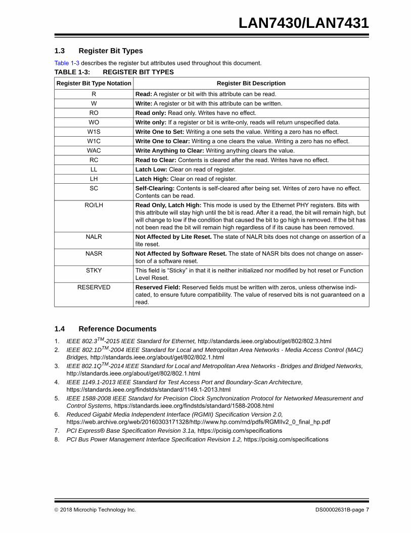
1.3 Register Bit Types
Table 1-3 describes the register but attributes used throughout this document.
TABLE 1-3: REGISTER BIT TYPES
Register Bit Type Notation Register Bit Description
R Read: A register or bit with this attribute can be read.
W Write: A register or bit with this attribute can be written.
RO Read only: Read only. Writes have no effect.
WO Write only: If a register or bit is write-only, reads will return unspecified data.
W1S Write One to Set: Writing a one sets the value. Writing a zero has no effect.
W1C Write One to Clear: Writing a one clears the value. Writing a zero has no effect.
WAC Write Anything to Clear: Writing anything clears the value.
RC Read to Clear: Contents is cleared after the read. Writes have no effect.
LL Latch Low: Clear on read of register.
LH Latch High: Clear on read of register.
SC Self-Clearing: Contents is self-cleared after being set. Writes of zero have no effect. Contents can be read.
RO/LH Read Only, Latch High: This mode is used by the Ethernet PHY registers. Bits with this attribute will stay high until the bit is read. After it a read, the bit will remain high, but will change to low if the condition that caused the bit to go high is removed. If the bit has not been read the bit will remain high regardless of if its cause has been removed.
NALR Not Affected by Lite Reset. The state of NALR bits does not change on assertion of a lite reset.
NASR Not Affected by Software Reset. The state of NASR bits does not change on asser-tion of a software reset.
STKY This field is “Sticky” in that it is neither initialized nor modified by hot reset or Function Level Reset.
RESERVED Reserved Field: Reserved fields must be written with zeros, unless otherwise indi-cated, to ensure future compatibility. The value of reserved bits is not guaranteed on a read.
1.4 Reference Documents
1. IEEE 802.3TM-2015 IEEE Standard for Ethernet, http://standards.ieee.org/about/get/802/802.3.html
2. IEEE 802.1DTM-2004 IEEE Standard for Local and Metropolitan Area Networks - Media Access Control (MAC) Bridges, http://standards.ieee.org/about/get/802/802.1.html
3. IEEE 802.1QTM-2014 IEEE Standard for Local and Metropolitan Area Networks - Bridges and Bridged Networks, http://standards.ieee.org/about/get/802/802.1.html
4. IEEE 1149.1-2013 IEEE Standard for Test Access Port and Boundary-Scan Architecture, https://standards.ieee.org/findstds/standard/1149.1-2013.html
5. IEEE 1588-2008 IEEE Standard for Precision Clock Synchronization Protocol for Networked Measurement and Control Systems, https://standards.ieee.org/findstds/standard/1588-2008.html
6. Reduced Gigabit Media Independent Interface (RGMII) Specification Version 2.0,https://web.archive.org/web/20160303171328/http://www.hp.com/rnd/pdfs/RGMIIv2_0_final_hp.pdf
7. PCI Express® Base Specification Revision 3.1a, https://pcisig.com/specifications
8. PCI Bus Power Management Interface Specification Revision 1.2, https://pcisig.com/specifications
2018 Microchip Technology Inc. DS00002631B-page 7
LAN7430/LAN7431
2.0 INTRODUCTION
2.1 General Description
The LAN7430/LAN7431 is a highly integrated PCIe to Gigabit Ethernet Controller, with IEEE Std 1588TM-2008 and advanced power management features, that provides a high performance and cost effective PCIe/Ethernet bridging solution for automotive and industrial applications.
The PCIe 3.1 PHY supports 1 Lane at 2.5GT/s for chip-to-chip and card-to-card connectivity across a combination of printed circuit boards, connectors, backplane wirings, and cables.
The LAN7430 has an integrated 10/100/1000 Ethernet PHY port with IEEE 802.3az Energy Efficient Ethernet (EEE) and 10BASE-Te support, while the LAN7431 supports either a RGMII (v1.3 and v2.0) or a MII MAC port for direct con-nectivity to transceivers, such as 100BASE-T1 or HDBaseT.
The LAN7430/LAN7431 further integrates PCIe Endpoint Controller, DMA Controller, Receive Filtering Engine, FIFO Controller, Ethernet MAC, EEPROM Controller, OTP Memory, TAP Controller, PME, and Clock/Reset/Power Manage-ment functions.
The IEEE1588-2008 PTP functions provide hardware support for the IEEE Std 1588-2008 (v2) Precision Time Protocol (PTP), allowing clock synchronization with remote Ethernet devices, packet time stamping, and time driven event gen-eration. The device may function as a master or a slave clock per the IEEE Std 1588-2008 specification. End-to-end and peer-to-peer link delay mechanisms are supported as are one-step and two-step operations.
Power Management functions include:
• Enabling the host to place the device in a reduced power state, by selectively disabling internal clocks, placing it into EEE Low Power Idle mode, and powering down the Ethernet PHY (LAN7430 only).
• Providing for detection of various wakeup events.
• Providing a host-readable READY flag which is set when the device is fully operational.
• Controlling the loading of OTP or EEPROM values after a system reset.
• Supporting D0 and D3hot and D3cold states
• Supporting L0s, L1 states and L1.1 and L1.2 Sub-states
Single 3.3V supply operation is achieved by enabling the on-chip Switching and LDO Regulators to supply the core and I/O voltages.
An internal EEPROM controller exists to load PCIe and MAC Address configuration parameters. For EEPROM-less applications, the LAN7430/LAN7431 provides 1K Bytes of OTP memory that can be used to preload this same config-uration data before enumeration.
The integrated IEEE 1149.1 compliant TAP controller provides boundary scan via JTAG.
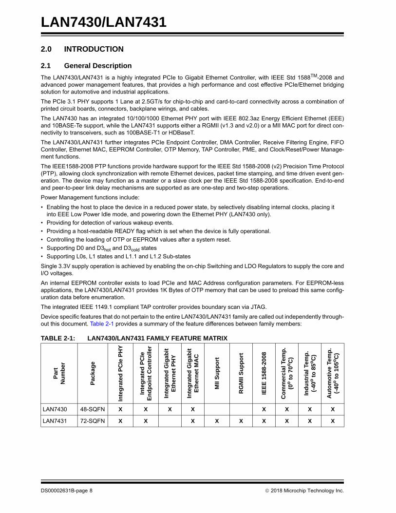
Device specific features that do not pertain to the entire LAN7430/LAN7431 family are called out independently through-out this document. Table 2-1 provides a summary of the feature differences between family members:
TABLE 2-1: LAN7430/LAN7431 FAMILY FEATURE MATRIX
Par
t N
um
ber
Pac
kag
e
Inte
gra
ted
PC
Ie P
HY
Inte
gra
ted
PC
Ie
En
dp
oin
t C
on
tro
ller
Inte
gra
ted
Gig
abit
E
ther
net
PH
Y
Inte
gra
ted
Gig
abit
E
ther
net
MA
C
MII
Su
pp
ort
RG
MII
Su
pp
ort
IEE
E 1
588
-20
08
Co
mm
erci
al T
em
p.
(0o t
o 7
0oC
)
Ind
ust
rial
Tem
p.
(-4
0o t
o 8
5oC
)
Au
tom
oti
ve T
emp
.(-
40o t
o 1
05oC
)
LAN7430 48-SQFN X X X X X X X X
LAN7431 72-SQFN X X X X X X X X X
DS00002631B-page 8 2018 Microchip Technology Inc.
LAN7430/LAN7431
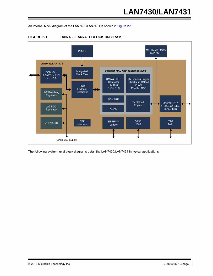
An internal block diagram of the LAN7430/LAN7431 is shown in Figure 2-1.
The following system-level block diagrams detail the LAN7430/LAN7431 in typical applications.
FIGURE 2-1: LAN7430/LAN7431 BLOCK DIAGRAM
LAN7430/ 1
DMA & FIFO ControllerTx Ch0
RxCh 0...3
GPIO 1588
OTPMemory
EEPROMLoader
PCIeEndpointController
Tx OffloadEngine
Ethernet PHY ++802.3az (EEE)
PCIe v3.1 2.5 GT / s PHY
++L1SS
1v2 SwitchingRegulator
2v5 LDORegulator
VDDVARIOJTAGTAP
Rx Filtering EngineChecksum Offload
VLAN Priority | RSS
NS / ARP
AOAC
Ethernet MAC with IEEE1588 2008IntegratedClock Tree
25 MHz MII / RGMII + (LAN7431)
Single 3v3 Supply
2018 Microchip Technology Inc. DS00002631B-page 9
LAN7430/LAN7431
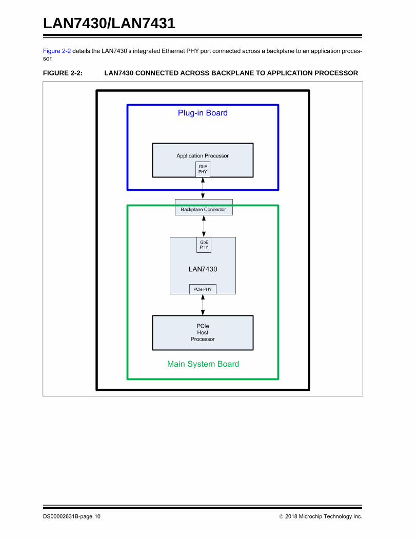
Figure 2-2 details the LAN7430’s integrated Ethernet PHY port connected across a backplane to an application proces-sor.
FIGURE 2-2: LAN7430 CONNECTED ACROSS BACKPLANE TO APPLICATION PROCESSOR
PCIeHost
Processor
LAN7430
PCIe PHY
GbE PHY
Backplane Connector
Application Processor
Main System Board
GbE PHY
Plug-in Board
DS00002631B-page 10 2018 Microchip Technology Inc.
LAN7430/LAN7431
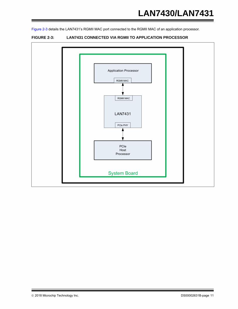
Figure 2-3 details the LAN7431’s RGMII MAC port connected to the RGMII MAC of an application processor.
FIGURE 2-3: LAN7431 CONNECTED VIA RGMII TO APPLICATION PROCESSOR
PCIeHost
Processor
LAN7431
PCIe PHY
Application Processor
System Board
RGMII MAC
RGMII MAC
2018 Microchip Technology Inc. DS00002631B-page 11

LAN7430/LAN7431
3.0 PIN DESCRIPTIONS AND CONFIGURATION
The pin assignments for the LAN7430 are detailed in Section 3.1, "LAN7430 Pin Assignments". The pin assignments for the LAN7431 are detailed in Section 3.2, "LAN7431 Pin Assignments". Pin descriptions are provided in Section 3.3, "Pin Descriptions".
3.1 LAN7430 Pin Assignments
The device pin diagram for the LAN7430 can be seen in Figure 3-1. Table 3-1 provides a LAN7430 pin assignments table. Pin descriptions are provided in Section 3.3, "Pin Descriptions".
FIGURE 3-1: LAN7430 PIN ASSIGNMENTS
Note: Configuration straps are identified by an underlined symbol name. Signals that function as configuration straps must be augmented with an external resistor when connected to a load.
Note: Exposed pad (VSS) on bottom of package must be connected to ground with a via field .
3
4
5
6
7
8
9
10
15
16
17
18
19
20
21
22
34
33
32
31
30
29
28
27
46
45
44
43
42
41
40
39
TXRXP_B
AVDDL_1
TXRXM_B
TXRXP_C
TXRXM_C
AVDDL_2
TXRXP_D
TXRXM_D
VDD12CORE
VDD
12C
OR
E
WA
KE
#
PER
ST#
38
37
48
47
1
2
11
12
13
14
23
24
26
25
36
35
TXRXM_A
TXRXP_A
VDD
VAR
IO
VAUX_DET/GPIO3/LED3/TCK
EED
IO/G
PIO
1/LE
D1/
TDO
EECLK/GPIO2/LED2/TMS/ADV_PM_DISABLE
PCIE_CLK_P
PCIE_CLK_M
VDD
12C
OR
E
AVD
D12
EEC
S/G
PIO
0/LE
D0/
TDI
XOISE
T
XI
VDD12_SW_FB
VDD_SW_IN
VDD
_OTP
VDD_REG_IN
VP
AVDDH_2
LAN743048-SQ FN
(Connect exposed pad to ground with a via field )
VSS
AVDDH_1C
LKR
EQ#
RESET_N
TEST
VPH
PCIE
_TX_
P
PC
IE_R
X_P
VPTX
PCIE
_RX_
M
GD_
2
RES
REF
GD_
1
PCIE
_TX_
M
GD_
3
VDD25_REG_OUT
VDD12_SW_OUT
DS00002631B-page 12 2018 Microchip Technology Inc.

LAN7430/LAN7431
TABLE 3-1: LAN7430 PIN ASSIGNMENTS
Pin Pin Name Pin Pin Name
1 AVDDH_1 25 PCIE_CLK_P
2 TXRXP_A 26 PCIE_CLK_M
3 TXRXM_A 27 VDD25_REG_OUT
4 AVDDL_1 28 VDD_REG_IN
5 TXRXP_B 29 RESET_N
6 TXRXM_B 30 TEST
7 TXRXP_C 31 VDD12CORE
8 TXRXM_C 32 VDD12_SW_OUT
9 AVDDL_2 33 VDD_SW_IN
10 TXRXP_D 34 VDD12_SW_FB
11 TXRXM_D 35 VAUX_DET/GPIO3/LED3/TCK
12 AVDDH_2 36 EECLK/GPIO2/LED2/TMS/ADV_PM_DISABLE
13 VDD12CORE 37 EEDIO/GPIO1/LED1/TDO
14 VP 38 EECS/GPIO0/LED0/TDI
15 GD_1 39 VDDVARIO
16 PCIE_RX_P 40 VDD12CORE
17 PCIE_RX_M 41 VDD_OTP
18 GD_2 42 CLKREQ#
19 PCIE_TX_P 43 WAKE#
20 VPTX 44 PERST#
21 PCIE_TX_M 45 AVDD12
22 GD_3 46 XO
23 VPH 47 XI
24 RESREF 48 ISET
Exposed Pad (VSS) must be connected to ground.
2018 Microchip Technology Inc. DS00002631B-page 13

LAN7430/LAN7431
3.2 LAN7431 Pin Assignments
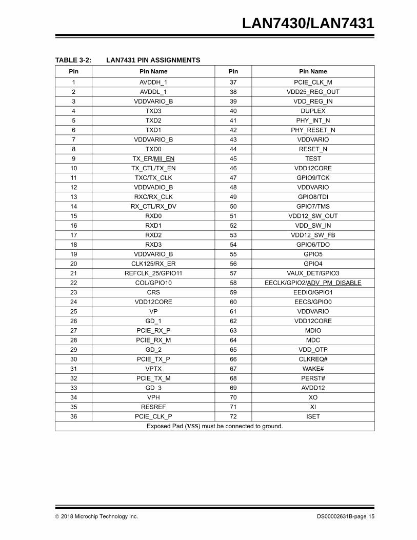
The device pin diagram for the LAN7431 can be seen in Figure 3-2. Table 3-2 provides a LAN7431 pin assignments table. Pin descriptions are provided in Section 3.3, "Pin Descriptions".
FIGURE 3-2: LAN7431 PIN ASSIGNMENTS
Note: Configuration straps are identified by an underlined symbol name. Signals that function as configuration straps must be augmented with an external resistor when connected to a load.
NOTE: Exposed pad (VSS) on bottom of package must be connected to ground
1
2
3
4
5
6
7
8
9
10
11
12
13
14
19
20
21
22
23
24
25
26
27
28
29
30
31
32
53
52
51
50
49
48
47
46
45
44
43
42
41
40
72 71 70 69 68 67 66 65 64 63 62 61 60
VDDVARIO_B
TXD3
TXD2
TXD1
VDDVARIO_B
TXD0
TX_CTL/TX_EN
TXC/TX_CLK
VDDVARIO_B
RXC/RX_CLK
AVD
D12
XIISET
XO
AVDDL_1
VDD
12C
OR
E
CLK
125/
RX_
ER
GPIO8/TDI
REF
CLK
_25/
GP
IO11
RX_CTL/RX_DV
TX_ER/MII_EN
DUPLEX
MD
C
MD
IO
15
16
17
18
59 58 57 56 55
39
38
37
33
34
35
RXD0
RXD1
CO
L/G
PIO
10
CR
SPE
RST#
36
54
RXD3
RXD2
PHY_RESET_N
PHY_INT_N
VDD
_OTP
VDDV
ARIO
_B
AVDDH_1
WA
KE#
TEST
VDD
12C
OR
E VP
VPH
PCIE
_TX_
P
PCIE
_RX_
P
VPTX
PCI
E_R
X_M
GD
_2
RESR
EF
GD
_1
PCIE
_TX_
M
GD
_3
PCIE
_CLK
_P
PCIE_CLK_M
VDD_REG_IN
VDD25_REG_OUT
VDDVARIO
RESET_N
VDD12CORE
GPIO9/TCK
VDDVARIO
GPIO7/TMS
VDD12_SW_FB
VDD_SW_IN
VDD12_SW_OUT
GPIO6/TDO
GPI
O5
GPI
O4
VAU
X_D
ET/G
PIO
3
EECS
/GPI
O0
EECL
K/G
PIO
2/A
DV_
PM_D
ISA
BLE
EEDI
O/G
PIO
1
VDD
VAR
IO
CLK
REQ
#
LAN743172-SQFN
(Connect exposed pad to ground with a via field )VSS
DS00002631B-page 14 2018 Microchip Technology Inc.
LAN7430/LAN7431
TABLE 3-2: LAN7431 PIN ASSIGNMENTS
Pin Pin Name Pin Pin Name
1 AVDDH_1 37 PCIE_CLK_M
2 AVDDL_1 38 VDD25_REG_OUT
3 VDDVARIO_B 39 VDD_REG_IN
4 TXD3 40 DUPLEX
5 TXD2 41 PHY_INT_N
6 TXD1 42 PHY_RESET_N
7 VDDVARIO_B 43 VDDVARIO
8 TXD0 44 RESET_N
9 TX_ER/MII_EN 45 TEST
10 TX_CTL/TX_EN 46 VDD12CORE
11 TXC/TX_CLK 47 GPIO9/TCK
12 VDDVADIO_B 48 VDDVARIO
13 RXC/RX_CLK 49 GPIO8/TDI
14 RX_CTL/RX_DV 50 GPIO7/TMS
15 RXD0 51 VDD12_SW_OUT
16 RXD1 52 VDD_SW_IN
17 RXD2 53 VDD12_SW_FB
18 RXD3 54 GPIO6/TDO
19 VDDVARIO_B 55 GPIO5
20 CLK125/RX_ER 56 GPIO4
21 REFCLK_25/GPIO11 57 VAUX_DET/GPIO3
22 COL/GPIO10 58 EECLK/GPIO2/ADV_PM_DISABLE
23 CRS 59 EEDIO/GPIO1
24 VDD12CORE 60 EECS/GPIO0
25 VP 61 VDDVARIO
26 GD_1 62 VDD12CORE
27 PCIE_RX_P 63 MDIO
28 PCIE_RX_M 64 MDC
29 GD_2 65 VDD_OTP
30 PCIE_TX_P 66 CLKREQ#
31 VPTX 67 WAKE#
32 PCIE_TX_M 68 PERST#
33 GD_3 69 AVDD12
34 VPH 70 XO
35 RESREF 71 XI
36 PCIE_CLK_P 72 ISET
Exposed Pad (VSS) must be connected to ground.
2018 Microchip Technology Inc. DS00002631B-page 15

LAN7430/LAN7431
3.3 Pin Descriptions
This section provides descriptions of each individual pin function. Buffer type definitions are detailed in Table 1-2.
TABLE 3-3: PIN DESCRIPTIONS
Name SymbolBuffer Type
Description
Gigabit Ethernet PHY Interface (LAN7430 only)
Ethernet TX/RX Positive
Channel A
TXRXP_A AIO Media Dependent Interface[0], positive signal of differen-tial pair
1000BT mode: TXRXP_A corresponds to BI_DA+ for MDI configuration and BI_DB+ for MDI-X configuration, respectively.
10BT/100BT mode: TXRXP_A is the positive transmit signal (TX+) for MDI configuration and the positive receive signal (RX+) for MDI-X configuration, respec-tively.
Ethernet TX/RX Negative
Channel A
TXRXM_A AIO Media Dependent Interface[0], negative signal of differen-tial pair
1000BT mode: TXRXM_A corresponds to BI_DA- for MDI configuration and BI_DB- for MDI-X configuration, respectively.
10BT/100BT-TX mode: TXRXM_A is the negative trans-mit signal (TX-) for MDI configuration and the negative receive signal (RX-) for MDI-X configuration, respectively.
Ethernet TX/RX Positive
Channel B
TXRXP_B AIO Media Dependent Interface[1], positive signal of differen-tial pair
1000BT mode: TXRXP_B corresponds to BI_DB+ for MDI configuration and BI_DA+ for MDI-X configuration, respectively.
10BT/100BT mode: TXRXP_B is the positive receive sig-nal (RX+) for MDI configuration and the positive transmit signal (TX+) for MDI-X configuration, respectively.
Ethernet TX/RX Negative
Channel B
TXRXM_B AIO Media Dependent Interface[1], negative signal of differen-tial pair
1000BT mode: TXRXM_B corresponds to BI_DB- for MDI configuration and BI_DA- for MDI-X configuration, respectively.
10BT/100BT mode: TXRXP_B is the negative receive signal (RX-) for MDI configuration and the negative trans-mit signal (TX-) for MDI-X configuration, respectively.
Ethernet TX/RX Positive
Channel C
TXRXP_C AIO Media Dependent Interface[2], positive signal of differen-tial pair
1000BT mode: TXRXP_C corresponds to BI_DC+ for MDI configuration and BI_DD+ for MDI-X configuration, respectively.
10BT/100BT mode: TXRXP_C is not used.
DS00002631B-page 16 2018 Microchip Technology Inc.
LAN7430/LAN7431
Ethernet TX/RX Negative
Channel C
TXRXM_C AIO Media Dependent Interface[2], negative signal of differen-tial pair
1000BT mode: TXRXM_C corresponds to BI_DC- for MDI configuration and BI_DD- for MDI-X configuration, respectively.
10BT/100BT mode: TXRXM_C is not used.
Ethernet TX/RX Positive
Channel D
TXRXP_D AIO Media Dependent Interface[3], positive signal of differen-tial pair
1000BT mode: TXRXP_D corresponds to BI_DD+ for MDI configuration and BI_DC+ for MDI-X configuration, respectively.
10BT/100BT mode: TXRXP_D is not used.
Ethernet TX/RX Negative
Channel D
TXRXM_D AIO Media Dependent Interface[3], negative signal of differen-tial pair
1000BT mode: TXRXM_D corresponds to BI_DD- for MDI configuration and BI_DC- for MDI-X configuration, respectively.
10BT/100BT mode: TXRXM_D is not used.
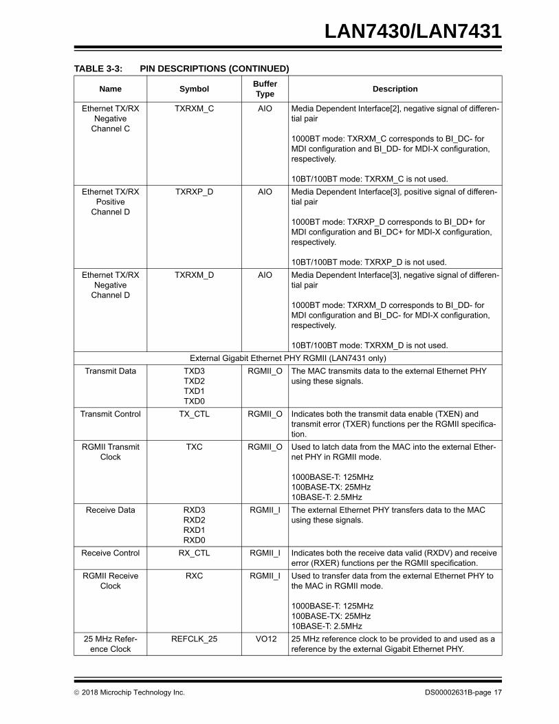
External Gigabit Ethernet PHY RGMII (LAN7431 only)
Transmit Data TXD3TXD2TXD1TXD0
RGMII_O The MAC transmits data to the external Ethernet PHY using these signals.
Transmit Control TX_CTL RGMII_O Indicates both the transmit data enable (TXEN) and transmit error (TXER) functions per the RGMII specifica-tion.
RGMII Transmit Clock
TXC RGMII_O Used to latch data from the MAC into the external Ether-net PHY in RGMII mode.
1000BASE-T: 125MHz100BASE-TX: 25MHz10BASE-T: 2.5MHz
Receive Data RXD3RXD2RXD1RXD0
RGMII_I The external Ethernet PHY transfers data to the MAC using these signals.
Receive Control RX_CTL RGMII_I Indicates both the receive data valid (RXDV) and receive error (RXER) functions per the RGMII specification.
RGMII Receive Clock
RXC RGMII_I Used to transfer data from the external Ethernet PHY to the MAC in RGMII mode.
1000BASE-T: 125MHz100BASE-TX: 25MHz10BASE-T: 2.5MHz
25 MHz Refer-ence Clock
REFCLK_25 VO12 25 MHz reference clock to be provided to and used as a reference by the external Gigabit Ethernet PHY.
TABLE 3-3: PIN DESCRIPTIONS (CONTINUED)
Name SymbolBuffer Type
Description
2018 Microchip Technology Inc. DS00002631B-page 17
LAN7430/LAN7431
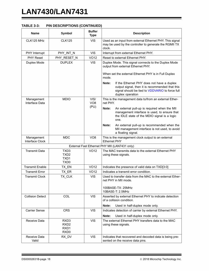
CLK125 MHz CLK125 VIS Used as an input from external Ethernet PHY. This signal may be used by the controller to generate the RGMII TX clock.
PHY Interrupt PHY_INT_N VIS Interrupt from external Ethernet PHY.
PHY Reset PHY_RESET_N VO12 Reset to external Ethernet PHY.
Duplex Mode DUPLEX VIS Duplex Mode. This signal connects to the Duplex Mode output from external Ethernet PHY.
When set the external Ethernet PHY is in Full Duplex mode.
Note: If the Ethernet PHY does not have a duplex output signal, then it is recommended that this signal should be tied to VDDVARIO to force full duplex operation
Management Interface Data
MDIO VIS/VO8(PU)
This is the management data to/from an external Ether-net PHY.
Note: An external pull-up is required when the MII management interface is used, to ensure that the IDLE state of the MDIO signal is a logic one.
Note: An external pull-up is recommended when the MII management interface is not used, to avoid a floating signal.
Management Interface Clock
MDC VO8 This is the management clock output to an external Ethernet PHY
External Fast Ethernet PHY MII (LAN7431 only)
Transmit Data TXD3TXD2TXD1TXD0
VO12 The MAC transmits data to the external Ethernet PHY using these signals.
Transmit Enable TX_EN VO12 Indicates the presence of valid data on TXD[3:0]
Transmit Error TX_ER VO12 Indicates a transmit error condition.
Transmit Clock TX_CLK VIS Used to transfer data from the MAC to the external Ether-net PHY in MII mode.
100BASE-TX: 25MHz10BASE-T: 2.5MHz
Collision Detect COL VIS Asserted by external Ethernet PHY to indicate detection of a collision condition.
Note: Used in half-duplex mode only.
Carrier Sense CRS VIS Indicates detection of carrier by external Ethernet PHY.
Note: Used in half-duplex mode only.
Receive Data RXD3RXD2RXD1RXD0
VIS The external Ethernet PHY transfers data to the MAC using these signals.
Receive Data Valid
RX_DV VIS Indicates that recovered and decoded data is being pre-sented on the receive data pins.
TABLE 3-3: PIN DESCRIPTIONS (CONTINUED)
Name SymbolBuffer Type
Description
DS00002631B-page 18 2018 Microchip Technology Inc.
LAN7430/LAN7431
Receive Error RX_ER VIS Asserted to indicate an error has been detected in the frame presently being transferred from the external Ethernet PHY.
Receive Clock RX_CLK VIS Used to transfer data from the external Ethernet PHY to the MAC in MII mode.
100BASE-TX: 25MHz10BASE-T: 2.5MHz
25 MHz Refer-ence Clock
REFCLK_25 VO12 25 MHz reference clock to be provided to and used as a reference by the external Fast Ethernet PHY.
PHY Interrupt PHY_INT_N VIS Interrupt from external Ethernet PHY.
PHY Reset PHY_RESET_N VO12 Reset to external Ethernet PHY.
Duplex Mode DUPLEX VIS Duplex Mode. This signal connects to the Duplex Mode output from external Ethernet PHY.
When set the external Ethernet PHY is in Full Duplex mode.
Note: If the external Ethernet PHY does not have a duplex output signal, then it is recommended that this signal should be tied to VDDVARIO to force full duplex operation
Management Interface Data
MDIO VIS/VO8(PU)
This is the management data to/from an external Ether-net PHY.
Note: An external pull-up is required when the MII management interface is used, to ensure that the IDLE state of the MDIO signal is a logic one.
Note: An external pull-up is recommended when the MII management interface is not used, to avoid a floating signal.
APPLICATION NOTE: A pull-up (internal or external) will result in a return value of FFFFh when a non-existent or non-addressed PHY is read. If a va lue of 0000h is des i red instead, a pull-down may be used.
Management Interface Clock
MDC VO8 This is the management clock output to an external Ethernet PHY
PCIe
TX Positive PCIE_TX_P AO PCIe Serial Data Output positive.
Serial differential output link in the PCIe interface running at 2.5 GT/s.
A series capacitor in the range of 100nF to 200nF is required.
TABLE 3-3: PIN DESCRIPTIONS (CONTINUED)
Name SymbolBuffer Type
Description
2018 Microchip Technology Inc. DS00002631B-page 19
LAN7430/LAN7431
TX Negative PCIE_TX_M AO PCIe Serial Data Output negative.
Serial differential output link in the PCIe interface running at 2.5 GT/s.
A series capacitor in the range of 100nF to 200nF is required.
RX Positive PCIE_RX_P AI PCIe Serial Data Input positive.
Serial differential input link in the PCIe interface running at 2.5 GT/s.
RX Negative PCIE_RX_M AI PCIe Serial Data Input negative.
Serial differential input link in the PCIe interface running at 2.5 GT/s.
External Refer-ence Clock
Positive
PCIE_CLK_P AI PCIe Differential Reference Clock In positive
This pin receives a 100 MHz differential clock input.
External Refer-ence Clock Negative
PCIE_CLK_M AI PCIe Differential Reference Clock In negative
This pin receives a 100 MHz differential clock input.
External Refer-ence Resistor
RESREF AI This pin should be connect to ground through a 200 ohm 1% 100 ppm / C resistor.
Wake up WAKE# IS / OD4 Wake
This signal is driven low when the device detects a wakeup.
In OBFF mode, OBFF events are signaled using the WAKE# pin as an input.
Note: When the device is powered down, this pin is isolated from the PCIe bus and does not present any significant loading or provide any drive.
PCIe Reset PERST# IS Power and Clock Good Indication
The PERST# signal indicates that both PCIe power and clock are available.
Note: When the device is powered down, this pin is isolated from the PCIe bus and does not present any significant loading or provide any drive.
Clock Request CLKREQ# IS / OD4 Clock Request
The CLKREQ# signal is used to power manage the Link clock. It is also used for L1 power management Sub state control.
Note: When the device is powered down, this pin is isolated from the PCIe bus and does not present any significant loading or provide any drive.
TABLE 3-3: PIN DESCRIPTIONS (CONTINUED)
Name SymbolBuffer Type
Description
DS00002631B-page 20 2018 Microchip Technology Inc.
LAN7430/LAN7431
Auxiliary Voltage Detect
VAUX_DET VIS(PD)
Auxiliary Voltage Detection
The VAUX_DET is used to indicate when PME from D3cold is supported.
When tied to VSS, PME from D3cold is not supported.The weak pull-down will create a logic low when plugged into a system board that does not support the delivery of the auxiliary voltage (the auxiliary voltage connection is floating).
When the device is powered exclusively from auxiliary voltage, this pin is tied to the auxiliary voltage (3.3V) to indicate PME from D3cold is supported.
When the device is powered from a multiplexed main voltage / auxiliary voltage, this pin is tied to the auxiliary voltage (3.3V) to indicate PME from D3cold is supported and to monitor the presence of the auxiliary voltage.
Note: If alternate usage of this pin (GPIO3, LED3 or TCK) is enabled, the pull-down is disabled and the input value of the pin is overridden to a low value.
Since this pin is shared with GPIO3, LED3 and TCK, a series resistor is recommended to prevent an accidental conflict with the auxiliary voltage. This resistor must be low enough in value to override the on chip pull-down.
Crystal / Oscillator / External Reference Clock
Crystal / Oscilla-tor / External Ref-
erence Clock Input
XI ICLK When using a 25MHz crystal, this input is connected to one lead of the crystal.
When using a 3.3V oscillator or external reference clock, this is the input from the clock source.
The crystal, oscillator, or external reference clock should have a tolerance of ±50ppm.
Crystal Output XO OCLK When using a 25MHz crystal, this output is connected to one lead of the crystal.
When using an oscillator or external clock source, this pin is not connected.
EEPROM
EEPROM Chip Select
EECS VO12(PD)
This pin drives the chip select input of the external EEPROM.
Note: The internal pull-down holds a low on the output pin during reset.
TABLE 3-3: PIN DESCRIPTIONS (CONTINUED)
Name SymbolBuffer Type
Description
2018 Microchip Technology Inc. DS00002631B-page 21
LAN7430/LAN7431
EEPROM Data In / Out
EEDIO VIS / VO12(PD)
This bidirectional pin is used for the EEPROM data. This pin directly drives the data input of the external EEPROM. The data output of the external EEPROM drives this pin through an external resistor.
Note: The internal pull-down holds a low on the pin during reset and provides a low on the input if an EEPROM is not connected.
Note: An external resistor, on the EEPROM’s data output, must be used to prevent contention during data read operations.
EEPROM Clock EECLK VO12(PD)
This pin drives the clock input of the external EEPROM.
Note: The internal pull-down holds a low on the output pin during reset.
Miscellaneous
GeneralPurpose I/O x
GPIO0GPIO1GPIO2GPIO3GPIO4GPIO5GPIO6GPIO7GPIO8GPIO9GPIO10GPIO11
VIS/VO8/VOD8(PU)
Each of these general purpose I/O pins is fully program-mable as either a push-pull output, an open-drain output, or a Schmitt-triggered input with pull-up.
Note: The pull-up is only enabled if the pin is set as a GPIO.
Note: GPIO0 through GPIO3 are available for the LAN7430 and LAN7431.
Note: GPIO4 through GPIO11 are available only for the LAN7431.
Test Pin TEST VIS(PD)
This pin is used to enable test modes and must be con-nected to ground for proper functional operation.
System Reset RESET_N VIS System reset. This pin is active low.
Note: If this signal is unused it must be pulled up to VDDVARIO.
Indicator LEDs LED0LED1LED2LED3
VOD12VOS12
(LAN7430 only)LED signal sourced from Gigabit Ethernet PHY.
Note: When enabled as LED outputs, the pins are either open-Drain or open-Source drivers.
External PHY Bias Resistor
ISET AI This pin should be connect to ground through a 6.04K 1% resistor.
JTAG
JTAG Test Mux Select
TMS VIS JTAG test mode select.
JTAG Test Clock TCK VIS JTAG test clock.
Note: The maximum operating frequency of this clock is half of the system clock.
JTAG Test Data Input
TDI VIS JTAG data input
JTAG Test Data Output
TDO VO12 JTAG data output.
TABLE 3-3: PIN DESCRIPTIONS (CONTINUED)
Name SymbolBuffer Type
Description
DS00002631B-page 22 2018 Microchip Technology Inc.
LAN7430/LAN7431
Configuration Straps
MII EnableConfiguration
Strap
MII_EN VIS(PD)
(LAN7431 only)When pulled high, the port operates in MII mode. When pulled low or floated, the port operates in RGMII mode. See Section 3.4, "Configuration Straps" for additional information.
Note: The internal pull-down is disabled once the strap is latched.
Note: If an external pull-up is used, it should be connected to VDDVARIO_B.
Advance Power Management Dis-
able Configuration
Strap
ADV_PM_DISABLE VIS(PD)
When pulled high, the following bits default low. When pulled low or floated, the register bits default high.
• Clock Power Management in Link Capabilities
• L1 PM Substates Supported in L1 PM Substates Capabilities
• ASPM L1.1 Supported in L1 PM Substates Capabili-ties
• ASPM L1.2 Supported in L1 PM Substates Capabili-ties
• PCI-PM L1.1 Supported in L1 PM Substates Capa-bilities
• PCI-PM L1.2 Supported in L1 PM Substates Capa-bilities
Note: Regardless of the strap default, the bits may be loaded from OTP or EEPROM. The default is used in the absence of a programmed OTP or EEPROM.
Note: The internal pull-down is disabled once the strap is latched.
Note: If an external pull-up is used, it should be connected to VDDVARIO.
Power / Ground
Ethernet PHY +1.2V Analog Power Supply
AVDD12 P 1.2V power for PLL/DLL
Ethernet PHY +2.5V / 3.3V Ana-log Power Supply
AVDDH_1 P 2.5V or 3.3V power for analog IO
LAN7430 onlyThis pin provides power for Gigabit PHY transmitter, bandgap reference, and crystal oscillator amplifier.
LAN7431 onlyThis pin provides power for bandgap reference and crys-tal oscillator amplifier.
Ethernet PHY +2.5V / 3.3V Ana-log Power Supply
AVDDH_2 P 2.5V or 3.3V power for analog IO
(LAN7430 only)This pin provides power for Gigabit PHY transmitter.
TABLE 3-3: PIN DESCRIPTIONS (CONTINUED)
Name SymbolBuffer Type
Description
2018 Microchip Technology Inc. DS00002631B-page 23

LAN7430/LAN7431
Ethernet PHY +1.2V Analog Power Supply
AVDDL_1 P 1.2V power for analog core
Ethernet PHY +1.2V Analog Power Supply
AVDDL_2 P 1.2V power for analog core
(LAN7430 only)This is an additional power pin for the 1.2V analog core.
PCIe PHY High Voltage Supply
VPH P 2.5V PCIe PHY power
PCIe PHY Trans-mit Supply
VPTX P 1.2V PCIe PHY TX power
PCIe PHY Analog and Digital Supply
VP P 1.2V PCIe PHY power
Variable I/O Power Supply Input Group A
VDDVARIO P 1.8V - 3.3V variable supply for IOs
Variable I/O Power Supply Input Group B
VDDVARIO_B P 1.8V - 3.3V variable supply for RGMII and MII related IOs
(LAN7431 only)This is the power pin for the RGMII and MII related IOs (TXD3, TXD2, TXD1, TXD0, TX_ER/MII_EN, TX_CTL/TX_EN, TXC/TX_CLK, RXC/RX_CLK, RX_CTL/RX_DV, RXD0, RXD1, RXD2, RXD3, CLK125/RX_ER, REF-CLK_25/GPIO11, COL/GPIO10, CRS).
OTP Power VDD_OTP P 3.3V to OTP charge pump
3.3V supply voltage for PCIe I/Os (CLKREQ#, WAKE#, PERST#)
Switcher Input Voltage
VDD_SW_IN P 1.8V - 3.3V input voltage for switching regulator
Switcher Feed-back
VDD12_SW_FB P Feedback pin for the integrated switching regulator
Note: Tie this pin to VDD_SW_IN to disable the switching regulator.
Switcher +1.2V Unfiltered Output
Voltage
VDD12_SW_OUT P 1.2V output voltage from switching regulator
LDO Input Voltage VDD_REG_IN P 3.3V input supply to the integrated LDO
Note: If this supply is set to 2.5V than it shall be externally connected to VDD25_REG_OUT. See Section 4.0, "Power Connectivity" for details.
LDO Output VDD25_REG_OUT P 2.5V output supply from the integrated LDO
This is used to supply power to the PCIE PHY and optionally to the Gigabit Ethernet PHY AFE.
Digital Core +1.2V Power Supply
Input
VDD12CORE P 1.2V digital core power.
TABLE 3-3: PIN DESCRIPTIONS (CONTINUED)
Name SymbolBuffer Type
Description
DS00002631B-page 24 2018 Microchip Technology Inc.
LAN7430/LAN7431
3.4 Configuration Straps
Configuration straps are latched on Power-On Reset (POR) and External Chip Reset (RESET_N) and are identified by an underlined symbol name. Configuration straps are multi-function pins that are driven as outputs during normal oper-ation. During a Power-On Reset (POR) or an External Chip Reset (RESET_N), these outputs are not driven. The high or low state of the signal is latched following deassertion of the reset and is used to determine the default configuration of a particular feature. The following configuration strap signals are available:
• ADV_PM_DISABLE
• MII_EN (LAN7431 only)
Configuration straps include internal resistors in order to prevent the signal from floating when unconnected. If a partic-ular configuration strap is connected to a load, an external pull-up or pull-down should be used to augment the internal resistor to ensure that it reaches the required voltage level prior to latching. The internal resistor can also be overridden by the addition of an external resistor. When externally pulling configuration straps high, the strap should be tied to VDDVARIO or VDDVARIO_B as indicated in the pin descriptions.
The system designer must ensure that configuration straps meet the timing requirements specified in Section 7.6.3, "Power-On Configuration Strap Timing" and Section 7.6.4, "Reset Pin Configuration Strap Timing". If configuration straps are not at the correct voltage level prior to being latched, the device may capture incorrect strap values.
PCIe Ground GD_1GD_2GD_3
P PCIe ground.
Ground VSS P Common ground.
This exposed pad must be connected to the ground plane with a via array.
Note: Configuration straps must never be driven as inputs. If required, configuration straps can be augmented, or overridden with external resistors.
TABLE 3-3: PIN DESCRIPTIONS (CONTINUED)
Name SymbolBuffer Type
Description
2018 Microchip Technology Inc. DS00002631B-page 25

LAN7430/LAN7431
4.0 POWER CONNECTIVITY
This section details the power connectivity of the LAN7430 and LAN7431 in various configurations. Power sequence timing is detailed in Section 7.6.2, "Power Sequence Timing".
4.1 LAN7430 Power Connectivity
The following diagrams illustrate the power connectivity for LAN7430 with on-chip regulators enabled and disabled.
FIGURE 4-1: LAN7430 POWER CONNECTIVITY ON-CHIP REGULATORS ENABLED
+1.8 V to +3.3 V
VDD12CORE
Core Logic &Ethernet PHY
digital
Ethernet PHY Analog
1.0 µF<1 ESRVSS
VDD12_SW_OUT
AVDD12
Ethernet PHY Bandgap and Osc
IO Pads
Note: Bypass and bulk caps as needed for PCB.Ferrites on AVDDL and AVDD12 may be combined.
VDDVARIO(1 pin)
VDD_SW_IN(1 pin)
+3.3 V
(1 pin)
(3 pins)
(2 pins)
(1 pin)
Ethernet PHY PLL
(exposed pad)
VDD25_REG_OUT
(1 pin)VDD12_SW_FB
VDD_REG_IN(1 pin)
3.3 / 1.2 OTPVDD_OTP(1 pin)
(1 pin)
AVDDH
AVDDL(2 pins)
PCIe PHY
VP(1 pin)
VPTX(1 pin)
VPH(1 pin)
3.3 uH
10 µF<0.05 ESR
0.1uF
+3.3 V
optional 3.3V PHY
operation
+1.8 V to +3.3 V
IN OUT
Internal 1.2 V Switching Regulator
FEEDBACKREF
IN OUT
Internal 2.5 V LDORegulator
ENABLE
DS00002631B-page 26 2018 Microchip Technology Inc.
LAN7430/LAN7431
FIGURE 4-2: LAN7430 POWER CONNECTIVITY ON-CHIP REGULATORS DISABLED
+1.8 V to +3.3 V
VDD12CORE
Core Logic &Ethernet PHY
digital
Ethernet PHY Analog
VSS
VDD12_SW_OUT
AVDD12
Ethernet PHY Bandgap and Osc
IO Pads
Note: Bypass and bulk caps as needed for PCB.Ferrites on AVDDL and AVDD12 may be combined.
VDDVARIO(1 pin)
+3.3 V
(1 pin)
(3 pins)
(2 pins)
(1 pin)
Ethernet PHY PLL
(exposed pad)
VDD25_REG_OUT
(1 pin)VDD12_SW_FB
VDD_REG_IN(1 pin)
3.3 / 1.2 OTPVDD_OTP(1 pin)
(1 pin)
AVDDH
AVDDL(2 pins)
PCIe PHY
VP(1 pin)
VPTX(1 pin)
VPH(1 pin)
+3.3 V
optional 3.3V PHY
operation
+1.8 V to +3.3 V
NCVDD_SW_IN(1 pin)
IN OUT
Internal 1.2 V Switching Regulator
FEEDBACKREF
+1.8 V to +3.3 V
+1.2 V
+2.5 V +2.5 V
IN OUT
Internal 2.5 V LDORegulator
ENABLE
2018 Microchip Technology Inc. DS00002631B-page 27

LAN7430/LAN7431
4.2 LAN7431 Power Connectivity
The following diagram illustrates the power connectivity for LAN7431 with on-chip regulators enabled and disabled.
FIGURE 4-3: LAN7431 POWER CONNECTIVITY ON-CHIP REGULATORS ENABLED
+1.8 V to +3.3 V
VDD12CORE
Core Logic &Ethernet PHY
digital
Ethernet PHY Analog
1.0 µF<1 ESRVSS
VDD12_SW_OUT
AVDD12
Ethernet PHY Bandgap and Osc
IO Pads
Note: Bypass and bulk caps as needed for PCB.Ferrites on AVDDL and AVDD12 may be combined.
VDDVARIO(7 pins)
+3.3 V
(1 pin)
(3 pins)
(1 pin)
(1 pin)
Ethernet PHY PLL
(exposed pad)
VDD25_REG_OUT
(1 pin)VDD12_SW_FB
VDD_REG_IN(1 pin)
3.3 / 1.2 OTPVDD_OTP(1 pin)
(1 pin)
AVDDH
AVDDL
PCIe PHY
VP(1 pin)
VPTX(1 pin)
VPH(1 pin)
3.3 uH
10 µF<0.05 ESR
0.1uF
+3.3 V
optional 3.3V PHY
operation
+1.8 V to +3.3 V
VDD_SW_IN(1 pin)
IN OUT
Internal 1.2 V Switching Regulator
FEEDBACKREF
(1 pin)
IN OUT
Internal 2.5 V LDORegulator
ENABLE
DS00002631B-page 28 2018 Microchip Technology Inc.
LAN7430/LAN7431
FIGURE 4-4: LAN7431 POWER CONNECTIVITY ON-CHIP REGULATORS DISABLED
+1.8 V to +3.3 V
VDD12CORE
Core Logic &Ethernet PHY
digital
Ethernet PHY Analog
VSS
VDD12_SW_OUT
AVDD12
Ethernet PHY Bandgap and Osc
IO Pads
Note: Bypass and bulk caps as needed for PCB.Ferrites on AVDDL and AVDD12 may be combined.
VDDVARIO(7 pins)
+3.3 V
(1 pin)
(3 pins)
(1 pin)
(1 pin)
Ethernet PHY PLL
(exposed pad)
VDD25_REG_OUT
(1 pin)VDD12_SW_FB
VDD_REG_IN(1 pin)
3.3 / 1.2 OTPVDD_OTP(1 pin)
(1 pin)
AVDDH
AVDDL
PCIe PHY
VP(1 pin)
VPTX(1 pin)
VPH(1 pin)
+3.3 V
optional 3.3V PHY
operation
+1.8 V to +3.3 V
VDD_SW_IN(1 pin)
IN OUT
Internal 1.2 V Switching Regulator
FEEDBACKREF
+2.5 V
NC
+1.8 V to +3.3 V
+2.5 V
+1.2 V
(1 pin)
IN OUT
Internal 2.5 V LDORegulator
ENABLE
2018 Microchip Technology Inc. DS00002631B-page 29

LAN7430/LAN7431
DS00002631B-page 30 2018 Microchip Technology Inc.
5.0 DEVICE CONFIGURATION
5.1 Device Drivers
Microchip provides LAN7430/LAN7431 software device drivers for the following operating systems:
• Windows 10
• Windows 8.x
• Windows 7
• Windows OneCore
• Linux
• Android
To download the latest LAN7430/LAN7431 drivers, refer to the Microchip product pages at www.microchip.com/LAN7430 and www.microchip.com/LAN7431.
5.2 Programming Tools
The LAN7430/LAN7431 supports a large number of configurable features. Microchip provides a comprehensive soft-ware programming tool, MPLAB Connect Configurator (formerly ProTouch2), for EEPROM and OTP configuration of various device functions and registers. All configuration is to be performed via the MPLAB Connect Configurator pro-gramming tool. For additional information on this tool, refer to th MPLAB Connect Configurator programming tool prod-uct page at http://www.microchip.com/design-centers/usb/mplab-connect-configurator.
Note: Device configuration straps are detailed in Section 3.4, "Configuration Straps," on page 25.Refer to Section 6.10, "EEPROM Controller (EEP)" and Section 6.11, "One Time Programmable Memory (OTP)" for detailed information on each device interface.

LAN7430/LAN7431
6.0 FUNCTIONAL DESCRIPTIONS
This section provides additional details of the major features supported by the LAN7430/LAN7431.
• PCI Express PHY (PCIe PHY)
• PCI Express Endpoint Controller (PCIe EP)
• Gigabit Ethernet Media Access Controller (MAC)
• RGMII (LAN7431 Only)
• Gigabit Ethernet PHY (GPHY) (LAN7430 Only)
• IEEE 1588v2 (PTP)
• Receive Filtering Engine (RFE)
• DMA Controller (DMAC)
• FIFO Controller (FCT)
• EEPROM Controller (EEP)
• One Time Programmable Memory (OTP)
• Resets
• Power Management
• Integrated Voltage Regulators
• JTAG
• Miscellaneous
6.1 PCI Express PHY (PCIe PHY)
The PCIe PHY forms the physical interface between the device’s PCIe endpoint control and the PCIe host bus. It sup-ports chip-to-chip and card-to-card connectivity across a combination of printed circuit board, connectors, backplane wiring or cables.
The PCIe PHY is compliant with all of the required features of the PCIe Base Specification, Revision 3.1 (for legacy 2.5 GT/s support).
The low power L1, L1.1 and L1.2 sub-states are supported per the PCIe Base 3.1 Specification.
6.1.1 FEATURES
• 2.5 GT/s data transmission rate
• PIPE3 compliant Transceiver Interface
• Integrated PHY includes transmitter, receiver, PLL, and digital core
• Programmable RX equalization
• Designed for excellent performance margin and receiver sensitivity
• Low jitter PLL technology with excellent supply isolation
The PHY supports a 2.5 GT/s data rate. Since bytes are encoded using the 8b/10b mechanism, this equates to a 2.0 Gbps data rate.
This device supports a PCIe link width of one lane.
6.1.2 REFERENCE CLOCK
The PHY utilizes an external 100MHz differential reference clock, supplied by the host system. PCIe architecture defines three clock distribution methods: common clock, data clock, and separate clock. The LAN7430/LAN7431 devices support the common clock method where both end devices, such as a host and the device, are using the same clock source. The details of the common clock method are provided in the PCIe specification.
6.1.3 TERMINATION RESISTANCE
The PHY includes on chip terminations for the TX and RX I/Os.
Termination on the PCIe reference clock pins is provided by the host.
6.1.3.1 Termination Resistance Tuning
The PHY uses an external resistor to calibrate the termination impedances of the high speed inputs and outputs of the PHY. A 200 Ohm +/-1% resistor should be connected from the RESREF pin to ground.
2018 Microchip Technology Inc. DS00002631B-page 31

LAN7430/LAN7431
6.1.4 TERMINATION CAPACITORS
The TX pins require series capacitors in the range of 100nF to 200nF.
6.1.5 BEACONING
The PHY supports the PCIe beaconing wake-up mechanism.
6.2 PCI Express Endpoint Controller (PCIe EP)
The device integrates a PCIe 3.1 Endpoint controller that includes the following common PCIe features:
• Split transaction, packet-based protocol
• Common flat address space for load/store access
- 32 and 64-bit memory address spaces
- I/O address space
- Configuration address space
• Transaction layer mechanism
• Credit-based flow control
• Various packet sizes and formats
• Reset and initialization
• Data integrity support
• Link layer retry for recovery following error detection
• 8b/10b encoding with running disparity
• In-band messaging
• Power management:
- Wake capability from D3cold state
- Compliant with ACPI, PCI-PM software model
- Active state power management
Additional functional features supported include:
• All non-optional features of the PCI Express Base 3.1 Specification
• The following optional features of the specification:
- Latency Tolerance Reporting (LTR)
- Completion Timeout Ranges
- Function Level Reset (FLR)
- L1 Substates (L1SS, L1.1SS, L1.2SS)
- Optimized Buffer Fill and Flush (OBFF)
- Readiness Notifications (RN)
- PCI Express Active State Power Management (ASPM)
- PCI Express Advanced Error Reporting (AER) with Multiple Header Logging
- Device Serial Number
- ECRC generation and checking
• x1 Gen1 Lane @ 2.5 GT/s
• Advanced Power and Clock Management
• Configurable Max_Payload_Size (128 bytes to 512 bytes)
• MSI and MSI-X with Per-Vector Masking (PVM)
• INTx Legacy interrupt emulation
• Type 0 Configuration space
DS00002631B-page 32 2018 Microchip Technology Inc.
LAN7430/LAN7431
6.3 Gigabit Ethernet Media Access Controller (MAC)
The Ethernet Media Access controller (MAC) incorporates the essential protocol requirements for operating an Ether-net/IEEE 802.3-compliant node and interfaces to the integrated Gigabit Ethernet PHY (LAN7430 only), or MII/RGMII interface (LAN7431 only). The MAC can operate in full-duplex 1000 Mbps or half/full-duplex 10/100 Mbps mode.
When operating in half-duplex mode, the MAC complies fully with Section 4 of ISO/IEC 8802-3 (ANSI/IEEE standard) and ANSI/IEEE 802.3 standards. When operating in full-duplex mode, the MAC complies with IEEE 802.3x full-duplex operation standard.
The MAC provides programmable enhanced features designed to minimize Host supervision, bus utilization, and pre- or post-message processing. These features include the ability to disable retries after a collision, dynamic FCS (Frame Check Sequence) generation on a frame-by-frame basis, automatic pad field insertion and deletion to enforce minimum frame size attributes, and automatic retransmission and detection of collision frames.
The primary attributes of the MAC are:
• Interfaces to the internal Gigabit Ethernet PHY (LAN7430 only), or MII/RGMII interface (LAN7431 only)
• Transmit and receive message data encapsulation
• Framing (frame boundary delimitation, frame synchronization)
• Error detection (physical medium transmission errors)
- Including Length Field testing
• FCS checking/stripping/generation
• Preamble stripping/generation
• Media access management
• Medium allocation (collision detection, except in full-duplex operation)
• Contention resolution (collision handling, except in full-duplex operation)
• Flow control during full-duplex mode
• Decoding of control frames (PAUSE command) and disabling the transmitter
• Generation of control frames (PAUSE command)
• Maintains minimum inter packet gap (IPG)
• Magic packet/Wake-On-LAN (WOL) detection
• Remote wakeup frame detection
• Neighbor Solicitation offload
• ARP offload
• Implements Simple Network Management Protocol (SNMP) and Remote Monitoring (RMON) management counter sets
• Jumbo frames supported up to 9220 bytes
6.4 RGMII (LAN7431 Only)
The integrated Reduced Gigabit Media Independent Interface (RGMII) is a Dual Data Rate (DDR) interface that consists of a transmit path and a receive path. Both paths have an independent clock (TXC & RXC), 4 data signals, and a control signal. Because of this design, RGMII does not have distinct PHY/MAC roles and special hardware considerations are not required for a MAC-to-MAC connection. When source-synchronous clocking is used for MAC-to-MAC connections, the clock signal that is output (by either path) is synchronous with the related data signals. This requires the PCB to be designed to add a 1.5-2 ns delay to the clock signal to meet the setup and hold times on the sink. The RGMII interface supports both Version 1.3 and Version 2.0 of the RGMII specification. Version 1.3 of the RGMII Specification requires a 1.5 to 2ns clock delay via a PCB trace delay. Version 2.0 of the RGMII Specification introduces the option of an on-chip Internal Delay (ID). These distinct RGMII modes of operation are referred to as “Non-ID Mode” and “ID Mode”, respec-tively.
The LAN7431 requires an external 125MHz clock reference on the CLK125 pin. The LAN7431 MAC may receive a 125 MHz reference clock from the partner PHY or MAC, which is used for generating the RGMII TXC signal. If this option is not available, the Generate CLK125 MHz Enable (CLK125_EN) field of the Hardware Configuration Register (HW_CFG) shall be set. When set, the device will generate the 125 MHz clock internally. For the processor MAC, sev-eral options are possible:
• The 125MHz clock reference is available internally.
2018 Microchip Technology Inc. DS00002631B-page 33
LAN7430/LAN7431
• The 125MHz clock is provided from an external clock source.
• The LAN7431 can output a 25MHz reference Clock that can be converted for generating the RGMII TXC Signal.
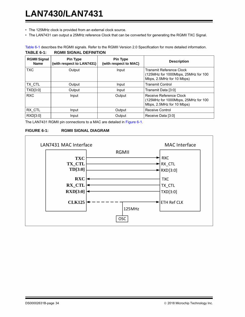
Table 6-1 describes the RGMII signals. Refer to the RGMII Version 2.0 Specification for more detailed information.
TABLE 6-1: RGMII SIGNAL DEFINITION
RGMII Signal Name
Pin Type (with respect to LAN7431)
Pin Type (with respect to MAC)
Description
TXC Output Input Transmit Reference Clock(125MHz for 1000Mbps, 25MHz for 100 Mbps, 2.5MHz for 10 Mbps)
TX_CTL Output Input Transmit Control
TXD[3:0] Output Input Transmit Data [3:0]
RXC Input Output Receive Reference Clock(125MHz for 1000Mbps, 25MHz for 100 Mbps, 2.5MHz for 10 Mbps)
RX_CTL Input Output Receive Control
RXD[3:0] Input Output Receive Data [3:0]
The LAN7431 RGMII pin connections to a MAC are detailed in Figure 6-1.
FIGURE 6-1: RGMII SIGNAL DIAGRAM
TXCTX_CTL
TD[3:0]
RXC
RX_CTL
RXD[3:0]
ETH Ref CLK
LAN7431 MAC Interface MAC Interface
TXC
TX_CTL
TXD[3:0]
RXC
RX_CTL
RXD[3:0]
CLK125
RGMII
OSC
125MHz
DS00002631B-page 34 2018 Microchip Technology Inc.

LAN7430/LAN7431
6.5 Gigabit Ethernet PHY (GPHY) (LAN7430 Only)
The device (LAN7430 only) incorporates a low-power Gigabit Ethernet PHY (GPHY) transceiver that is fully compliant with the IEEE 802.3, 802.3u, 802.3ab, and 802.3az (Energy Efficient Ethernet) standards. It provides a low electromag-netic interference (EMI) line driver, and integrated line side termination resistors that conserve both power and printed circuit board (PCB) space.
The mixed signal and digital signal processing (DSP) architecture of the Ethernet PHY assures robust performance even under less-than-favorable environmental conditions. It supports both half-duplex and full-duplex 10BASE-T and 100BASE-TX, and full-duplex 1000BASE-T communication speeds over Category 5 (Cat5) unshielded twisted pair (UTP) cable at distances greater than 100m, displaying excellent tolerance to NEXT, FEXT, echo, and other types of ambient environment and system electronic noise. The Ethernet PHY implements Auto-Negotiation to automatically determine the best possible speed and duplex mode of operation. Auto-MDIX support allows the use of direct connect or cross-over LAN cables.
The Ethernet PHY is configurable via the Ethernet PHY Control and Status. These registers are accessed indirectly through the Ethernet MAC via the MII Access Register (MII_ACCESS) and MII Data Register (MII_DATA).
The Gigabit Ethernet PHY has the following main features:
• Auto-Negotiation to Automatically Select the Highest Link-Up Speed (10/100/1000 Mbps) and Duplex (Half/Full)
• Voltage-mode Line driver with On-Chip Termination Resistors for the Differential Pairs
• Jumbo Frame Support Up to 16 KB (MAC supports 9220 bytes)
• Energy-Detect Power-Down Mode for Reduced Power Consumption When the Cable is not attached
• Energy Efficient Ethernet (EEE) Support with Low-Power Idle (LPI) Mode and Clock Stoppage for 100BASE-TX/1000BASE-T and Transmit Amplitude Reduction with 10BASE-Te Option
• Programmable LED Outputs for Link, Activity, and Speed
• Baseline Wander Correction
• TDR-based Cable Diagnostic to Identify Faulty Copper Cabling
• Loopback Modes for Diagnostics
• Automatic MDI/MDI-X Crossover to Detect and Correct Pair Swap at All Speeds of Operation
• Automatic Detection and Correction of Pair Swaps, Pair Skew, and Pair Polarity
• Power-Down and Power-Saving Modes
• Signal Quality Indication
6.6 IEEE 1588v2 (PTP)
The device provides hardware support for the IEEE 1588-2008 (v2) Precision Time Protocol (PTP), allowing clock syn-chronization with remote Ethernet devices, packet time stamping, and time driven event generation.
The device may function as a master or a slave clock per the IEEE 1588-2008 specification. End-to-end and peer-to-peer link delay mechanisms are supported as are one-step and two-step operations.
A 32-bit seconds and 30-bit nanoseconds tunable clock is provided that is used as the time source for all PTP timestamp related functions. A 1588 Clock Events sub-module provides 1588 Clock comparison based interrupt generation and timestamp related GPIO event generation. GPIO pins can be used to trigger a timestamp capture when configured as an input, or output a signal based on a 1588 Clock timer compare event.
All features of the IEEE 1588 unit can be monitored and configured via their respective configuration and status regis-ters.
6.6.1 IEEE 1588-2008
IEEE 1588-2008 specifies a Precision Time Protocol (PTP) used by master and slave clock devices to pass time infor-mation in order to achieve clock synchronization. Ten network message types are defined:
• Sync
• Follow_Up
• Delay_Req
• Delay_Resp
• PDelay_Req
• PDelay_Resp
2018 Microchip Technology Inc. DS00002631B-page 35

LAN7430/LAN7431
• PDelay_Resp_Follow_Up
• Announce
• Signaling
• Management
The first seven message types are used for clock synchronization. Using these messages, the protocol software may calculate the offset and network delay between timestamps, adjusting the slave clock frequency as needed. Refer to the IEEE 1588-2008 protocol for message definitions and proper usage.
A PTP domain is segmented into PTP sub-domains, which are then segmented into PTP communication paths. Within each PTP communication path there is a maximum of one master clock, which is the source of time for each slave clock. The determination of which clock is the master and which clock(s) is(are) the slave(s) is not fixed, but determined by the IEEE 1588-2008 protocol. Similarly, each PTP sub-domain may have only one master clock, referred to as the Grand Master Clock.
PTP communication paths are conceptually equivalent to Ethernet collision domains and may contain devices which extend the network. However, unlike Ethernet collision domains, the PTP communication path does not stop at a net-work switch, bridge, or router. This leads to a loss of precision when the network switch/bridge/router introduces a vari-able delay. Boundary clocks are defined which conceptually bypass the switch/bridge/router (either physically or via device integration). Essentially, a boundary clock acts as a slave to an upstream master, and as a master to a down stream slave. A boundary clock may contain multiple ports, but a maximum of one slave port is permitted.
Although boundary clocks solve the issue of the variable delay influencing the synchronization accuracy, they add clock jitter as each boundary clock tracks the clock of its upstream master. Another approach that is supported is the concept of transparent clocks. These devices measure the delay they have added when forwarding a message (the residence time) and report this additional delay either in the forwarded message (one-step) or in a subsequent message (two-step).
The PTP relies on the knowledge of the path delays between the master and the slave. With this information, and the knowledge of when the master has sent the packet, a slave can calculate its clock offset from the master and make appropriate adjustments. There are two methods of obtaining the network path delay. Using the end-to-end method, packets are exchanged between the slave and the master. Any intermediate variable bridge or switch delays are com-pensated by the transparent clock method described above. Using the round trip time and accounting for the residence time reported, the slave can calculate the mean delay from the master. Each slave sends and receives its own mes-sages and calculates its own delay. While the end-to-end method is the simplest, it does add burden on the master since the master must process packets from each slave in the system. This is amplified when boundary clocks are replaced by transparent clocks. Also, the end-to-end delays must be recalculated if there is a change in the network topology. Using the peer-to-peer method, packets are exchanged only between adjacent master, slaves and transparent clocks. Each peer pair calculates the receive path delay. As time synchronization packets are forwarded between the master and the slave, the transparent clock adds the pre-measured receive path delay into the residence time. The final receiver adds its receive path delay. Using the peer-to-peer method, the full path delay is accounted for without the mas-ter having to service each slave. The peer-to-peer method better supports network topology changes since each path delay is kept up-to-date regardless of the port status.
The PTP implementation consists of the following major function blocks:
• PTP TimestampThis block provides time stamping and packet modification functions.
• 1588 ClockThis block provides a tunable clock that is used as the time source for all PTP timestamp related functions.
• 1588 Clock EventsThis block provides clock comparison-based interrupt generation and timestamp related GPIO event generation.
• 1588 GPIOsThis block provides for time stamping GPIO input events and for outputting clock comparison-based interrupt sta-tus.
• 1588 InterruptsThis block provides interrupt generation, masking and status.
• 1588 RegistersThis block provides contains all configuration, control and status registers.
DS00002631B-page 36 2018 Microchip Technology Inc.
LAN7430/LAN7431
6.7 Receive Filtering Engine (RFE)
The RFE receives Ethernet frames from the Ethernet MAC, processes them, and passes them to the RX FIFO Controller (FCT). The RFE is responsible for filtering the received Ethernet frames, verifying the TCP/UDP/ICMP/IGMP and IP checksum, and removing the VLAN tag.
When receiving a frame from the MAC, the RFE will obtain the frame data and status information. Upon completion of frame processing, the RFE encapsulates its status with the status information obtained from the MAC, and passes this information (along with the frame data) on to the FCT in the form of RX Command A, RX Command B, RX Command C and RX Command D. The RFE also passes the receive timestamp from the 1588 module to the FCT.
The RFE, if enabled, can remove a VLAN tag from the frame. VLAN tag stripping is controlled by the Enable VLAN Tag Stripping bit of the Receive Filtering Engine Control Register (RFE_CTL). If this bit is set, the tag will be stripped. If clear, the RFE will not modify the frame in any way.
If multiple VLAN tags are present in a frame, the RFE only removes the first tag (adjacent to the MAC source address).
The RFE provides the Layer 3 Checksum (if enabled) and VLAN ID via RX Command B, while RX Command A, RX Command C and RX Command D contain the frame’s status.
When the RFE determines a frame has a checksum error, it sets the appropriate error bits in RX Command A to identify the error condition.
The FCT does not rewind frames that failed checksum validation from the FCT RX FIFO.
The RFE also determines the correct RX FCT channel in which to place the frame, based on various priorities methods or MAC source or destination address or based on the Microsoft Receive Side Scaling specification. In order to minimize delays through the RFE, data is processed on the fly and stored into all FIFOs in parallel. Once a determination is made as to the correct destination FIFOs, the other FIFOs are instructed to drop the packet.
6.8 DMA Controller (DMAC)
The DMA Controller (DMAC) consists of independent receive (RX) and transmit (TX) DMACs, a series of arbiters, and a control and status register space (CSRs). The TX DMAC transfers Ethernet frames from host memory to the FIFO Controller (FCT), while the RX DMAC transfers Ethernet frames from the FCT to host memory. Both the RX and TX DMACs have independent channels allocated to them (4 RX, 1 TX), through which the data transfer occurs.
Both the RX and TX DMACs utilize descriptors to efficiently move data from source to destination with minimal CPU intervention. Descriptors are data structures in host memory that inform the DMAC of the location of data buffers in host memory. In the case of the RX DMAC, it also provides a mechanism for communicating status to the CPU on completion of DMA transactions. The host is responsible for setting up the descriptor rings and allocating RX descriptor buffers. TX descriptor buffers are allocated and placed into the ring as needed. Each channel has its own descriptor ring and data buffers. Descriptors are cached on chip to help absorb host bus latency.
The DMAC can be programmed to assert an interrupt for situations such as frame transmit or receive transfer com-pleted, and other conditions.
6.9 FIFO Controller (FCT)
The FIFO controller uses internal RAMs to buffer RX and TX traffic. Host transmit data, via the DMAC, is directly stored into the FCT TX FIFO(s). The FCT is responsible for extracting Ethernet frames from the host data and passing the frames to the MAC.
Received Ethernet Frames are stored into the FCT RX FIFOs and become the basis for DMAC to host memory trans-fers.
6.9.1 RX PATH (ETHERNET TO HOST)
The Receive direction buffer space consists of four parallel, independent channels. Each of the four 32 KB RX FIFOs buffer Ethernet frames received from the RFE. The DMAC transfers these frames from the FCT to the host system mem-ory. Host software will ultimately reassemble the Ethernet frames from the DMAC transfers.
2018 Microchip Technology Inc. DS00002631B-page 37
LAN7430/LAN7431
6.9.2 TX PATH (HOST TO ETHERNET)
The 20 KB TX FIFO buffers data transferred by the DMAC from system memory. The FCT is responsible for extracting the Ethernet frames embedded in the data and passing them to the MAC.
The FCT receives valid data from the DMAC and writes it into the TX FIFO. The write side of the FCT does not perform any processing on the data. No provisions for rewind on the write side are required, as the DMAC manages its own buffer RAM and performs rewinds in the event that a DMA transfer is errored. When the FCT writes the Ethernet frame into the FCT TX FIFO RAM, it prepends a DWORD in front of the TX Command Words, used for internal processing, that contains the length of the Ethernet frame. The read side of the FCT TX FIFO is responsible for extracting the Ether-net frames.
6.10 EEPROM Controller (EEP)
The device may use an external EEPROM to store the default values for the PCIe controller and the MAC address. The EEPROM controller supports most “93C56 or 93C66” type 256/512 byte EEPROMs. A total of nine address bits are used.
After a system-level reset occurs, the device loads the default values from EEPROM. The device is connected to the PCIe bus but responds with CRS until this process is completed. The EEPROM controller also allows the Host to read, write and erase the contents of the Serial EEPROM.
Note: All EEPROM configuration is to be performed via the MPLAB Connect Configurator programming tool. Refer to Section 5.2, "Programming Tools" for additional information.
Note: A Microwire-style 2K/4K EEPROM that is organized for 256/512 x 8-bit operation must be used.
6.10.1 EEPROM AND OTP RELATIONSHIP
A detected external EEPROM alway takes precedence over the OTP. When determining the source to configure the device the following order is used.
1. EEPROM Configuration
2. OTP Configuration
3. CSR defaults
The Configuration and Status Registers defaults are used if neither the EEPROM nor OTP is determined to be config-ured.
6.10.2 EEPROM / OTP AUTO-LOAD
Certain system level resets (PCIe Fundamental Reset, Hot Resets, Function-Level Reset (FLR), Power Management Soft Reset, Power-On Reset (POR), External Chip Reset (RESET_N) and Soft Reset) may cause the EEPROM or OTP contents to be auto-loaded into the device.
Depending on the reset event, either the PCIe Configuration registers, the system Configuration Status Registers, or both are programmed. See Section 6.12, "Resets" for additional information.
6.10.2.1 Magic Byte
6.10.2.1.1 EEPROM
After a reset, the EEPROM loader attempts to read the first byte of data from the EEPROM. If the value A5h or AAh is read from the first address, then the EEPROM loader will assume that a programmed external Serial EEPROM is pres-ent. A value of AAh in the first address indicates that only the MAC address is to be read and used.
6.10.2.1.2 OTP
As with the EEPROM, a signature is required to define whether or not the OTP has been programmed. If the value F3h or F7h is found at byte 0, the OTP shall be determined to be programmed.
APPLICATION NOTE: Certain reset events cause a restoration from previously read EEPROM / OTP values rather than rereading the EEPROM or OTP.
DS00002631B-page 38 2018 Microchip Technology Inc.

LAN7430/LAN7431
A signature of F3h indicates that the device is configured using values (MAC Address and subsequent as per EEPROM Contents) from byte offset 1 in the OTP. A value of F7h indicates that the device is configured loading values (MAC Address and subsequent as per EEPROM Contents) from byte offset 513 in the OTP.
As with the EEPROM, if a valid signature is not present at byte 0, the OTP shall be deemed to not be programmed and the hardware shall not use it for configuring the device. Unlike the EEPROM, there is no signature value (e.g. AAh) that indicates that only the MAC address is to be loaded.
6.10.2.2 Blank / No EEPROM
If A5h or AAh (EEPROM) or F3h or F7h (OTP) is not read from the first address, the EEPROM loader will end initializa-tion. The device default values will be assumed unless a configured OTP is present.
Where there is no EEPROM or OTP, it is the responsibility of the Host LAN driver software to set the IEEE 802.3 address by writing to the MAC Receive Address High Register (RX_ADDRH) and MAC Receive Address Low Register (RX_AD-DRL).
6.11 One Time Programmable Memory (OTP)
The device integrates a 1K One Time Programmable (OTP) memory to store various configuration data and serve as an EEPROM replacement to reduce bill of material costs. The OTP supports single bit writes and 8-bit reads. An included OTP interrupt is available to indicate when the OTP is ready. The OTP provides a configurable standby mode that reduces its power when operations have been completed.
OTP may potentially co-exist with an external EEPROM. Refer to Section 6.10.1, "EEPROM and OTP Relationship" for additional details.
Certain system level resets may cause the OTP contents to be auto-loaded into the device. Refer to Section 6.10.2, "EEPROM / OTP Auto-Load" for additional details.
Note: All OTP configuration is to be performed via the MPLAB Connect Configurator programming tool. Refer to Section 5.2, "Programming Tools" for additional information.
6.12 Resets
The device provides the following chip-level reset sources:
• Power-On Reset (POR)
• External Chip Reset (RESET_N)
• PCIe Fundamental Reset
• Hot Resets
• Function-Level Reset (FLR)
• Soft Reset
• Soft-Lite Reset
• Power Management Soft Reset
Additionally, the device provides non-chip-level resets:
• Ethernet PHY Software Reset
• External PHY Reset
APPLICATION NOTE: The dual signatures enable a mechanism for the OTP to be programmed twice. This may prove useful for initial bring up of the device where inadvertently mis-programming the device could render it non-functional. This scheme requires that when an signature of F3h is used that only the first 512 bytes (0 through 511) of the OTP are programmed. In the event that the OTP was mis-configured the device can be “saved” by changing the signature on byte 0 from F3h to F7h and writing the new content starting at byte 513.
2018 Microchip Technology Inc. DS00002631B-page 39

LAN7430/LAN7431
6.12.1 POWER-ON RESET (POR)
A Power-On Reset (POR) occurs whenever power is initially applied to the device, or if power is removed and reapplied to the device. A timer within the device will assert the internal reset for approximately 20 ms. EEPROM/OTP contents are loaded by this reset. Configuration straps are also loaded by this reset.
The POR is a combination of four separate POR circuits that measure the voltage on the following domains:
• 3.3V to 1.8V (set for 1.8V typical) - VDDVARIO, VDDVARIO_B
• 1.2V - AVDD12, AVDDL_1, AVDDL_2, VPTX, VP, VDD12CORE (monitored on AVDD12 and VDD12CORE)
• 2.5V - VPH, AVDDH_1, AVDDH_2 (monitored on VDD25_REG_OUT)
• 3.3V - VDD_OTP, AVDDH_1, AVDDH_2 (monitored on VDD_OTP)
6.12.2 EXTERNAL CHIP RESET (RESET_N)
A hardware reset will occur when the RESET_N pin is driven low. Assertion of RESET_N is not required at power-on. However, if used, RESET_N must be driven low for a minimum period as defined in Section 7.6.4, "Reset Pin Configu-ration Strap Timing". The RESET_N pin is not pulled-high internally and must be connected to VDDVARIO if unused.
Note: If configured, the EEPROM/OTP contents are reloaded by this reset. The configuration straps are also loaded by this reset.
6.12.3 PCIE FUNDAMENTAL RESET
The PCIe fundamental reset uses the PERST# pin, which indicates that the PCIe main power and reference clock are valid. It is used as a cold reset when the device operates from the main PCIe power source. It is used as a warm reset when the device operates from the auxiliary PCIe power source and indicates, to the still powered and operational device, that the main power and / or reference clock are not valid.
Note: Resets occur on the release of PERST#, not on the active level.
6.12.3.1 Warm Reset
A warm reset occurs when the device is operating on auxiliary power or multiplexed main / auxiliary power (VAUX_DET pin = 1) and PERST# is asserted. The device enters the D3cold state. Warm reset is normally preceded by the PCIe link being placed into the L2/L3 Ready state. The D3cold state is exited when PERST# deasserts.
6.12.4 HOT RESETS
Hot resets include
• An in-band mechanism for propagating Conventional Reset across a Link
• An in-band mechanism for software to force a Link into Electrical Idle, disabling the Link
• The Data Link Layer reporting DL_Down status.
6.12.5 FUNCTION-LEVEL RESET (FLR)
Function-Level Reset is a software issued reset triggered when the Initiate Function Level Reset bit in the PCIe Device Control configuration register is set. It is used to reset the device without affection the link state. An FLR starts, is pro-cessed and then exits.
During an FLR:
• All requests and completions for the function that arrived from the wire before the FLR started are handled by silently dropping them.
• All requests following the FLR are discarded using Unsupported Request (UR) (for posted and non-posted requests), and using Unexpected Completion (UC) for completions. Therefore, the software driver should put the function into a quiescent state (by clearing the BME or otherwise) before initiating an FLR so that the function does not issue requests in close proximity to the FLR event. Otherwise, any completions from these requests will dropped later on.
• The function should not issue requests during FLR. Otherwise, completions from these requests (received by the device after the function has exited FLR) are treated as unexpected and dropped.
• Any outstanding INTx interrupt asserted by the function must be deasserted by sending the corresponding Deas-sert_INTx Message.
DS00002631B-page 40 2018 Microchip Technology Inc.
LAN7430/LAN7431
• The device’s non-PCIe functionality is reset.
• The FLR routine exits.
6.12.6 SOFT RESET
This is a software issued reset when the Soft Reset (SRST) bit in the Hardware Configuration Register (HW_CFG) is set. It is used to completely reset the device as if it was a cold reset.
As with a POR and RESET_N:
• The entire device is reset.
• A timer within the device will assert the internal reset for approximately 20 ms.
• The EEPROM/OTP contents are loaded by this reset.
Note: This reset will cause a detach from the PCIe bus, which may cause host software issues if unexpected.
6.12.7 SOFT-LITE RESET
This is a software issued reset when the Soft Lite Reset (LRST) bit in the Hardware Configuration Register (HW_CFG) is set. It is used to reset only the device function without resetting the PCIe portion.
Note: Software must stop all RX and TX channels of the DMA controller before setting this bit.Software must disable all interrupts before setting this bit.Software must not access any device Control and Status Registers (PCIe Configuration Space registers excluded) for at least 5µS after setting Soft Lite Reset (LRST).Software should verify that Soft Lite Reset (LRST) has self-cleared before performing any device opera-tions or setting any device CSRs (PCIe Configuration Space registers excluded)
6.12.8 POWER MANAGEMENT SOFT RESET
This reset is created when the device’s power state is changed from D3hot to D0u by writing a 00b to the PowerState field in the Power Management Control/Status PCIe configuration register while the No_Soft_Reset field is clear.
6.12.9 ETHERNET PHY SOFTWARE RESET
The Ethernet PHY software reset is triggered via the Ethernet PHY Reset (ETH_PHY_RST) bit in the Power Manage-ment Control Register (PMT_CTL). It holds the Ethernet PHY reset for a minimum of 2 ms.
For the LAN7431 (external Ethernet PHY), the PHY_RESET_N pin is asserted during this reset. The Device Ready (READY) bit in the Power Management Control Register (PMT_CTL) asserts after the 2 ms PHY_RESET_N assertion interval completes. An optional 125ms delay can be enabled to allow for the external PHY to become ready. This is enabled with the External PHY Ready Delay Enable (EXT_PHY_RDY_EN) bit.
For the LAN7430 (internal Ethernet PHY), the Device Ready (READY) asserts when the internal PHY is functional, fol-lowing the reset.
6.12.10 EXTERNAL PHY RESET
The LAN7431 uses the dedicated PHY_RESET_N pin for automatically resetting the external Ethernet PHY. This pin automatically asserts as part of the reset sequence. The PHY_RESET_N may also be asserted by an Ethernet PHY Software Reset.
APPLICATION NOTE: Although some registers are returned to their last EEPROM or OTP specified default upon a Soft Like Reset (LRST), the device does not automatically reload its full configuration (including the User Initialization Table) from OTP or EEPROM. If necessary or desired, software may issue a Host Initiated EEPROM or OTP Reload.
Note: The Ethernet PHY Software Reset is not a chip-level reset. It resets only the Ethernet PHY.
2018 Microchip Technology Inc. DS00002631B-page 41

LAN7430/LAN7431
6.13 Power Management
The device supports two categories of Power Management (PM) operations to control the device state (D-state) and link state of the PCIe PHY and Endpoint Controller functional blocks.
Software PCI Compatible PM (PCI-PM) allows the host software to direct the function to enter into the D3hot and D3coldlow-power states. This indirectly causes a change in the link power state. The L1 state is entered when the device is programmed to a non-D0 state. Further entry into L1.1 and L1.2 sub-states is initiated by the downstream port. Clock power management during the L1 state provides for the removal of the PCIe reference clock.
Native PCIe PM Mechanisms include Active State PM (ASPM) which, while in the L0 state, detects idle on the link for a specific time duration and automatically transitions the link to the L0s or L1 power states. L1 Sub-states are also sup-ported that disables components on a link to further reduce idle power consumption while the link is in the L1 state, including almost complete removal of power for the high speed PHY circuits.
The power management functions include:
• Enabling the host to place the device in a reduced power state, by selectively disabling internal clocks and power-ing down the Ethernet PHY (LAN7430 only).
• Providing for detection of various wakeup events.
• Providing a host-readable READY flag which is set when the device is fully operational.
• Controlling the loading of OTP or EEPROM values after a system reset.
• Supporting D0 and D3hot and D3cold states
• Supporting L0s, L1 states and L1.1 and L1.2 Sub-states
Power Management Event (PME) functions include:
• Supporting PCIe WAKE# and Beaconing.
• Supporting PCIe PME Messaging.
• Supporting GPIO, Link Change, Ethernet Frame as sources for wakeup.
6.13.1 PCIe DEVICE STATES
The device supports the mandatory D0 (herein referred to as D0u (uninitialized), D0a (active)), D3hot, and D3cold power states. The optional D1 and D2 states are not support by the device.
The device can signal a wake event detection by sending a PME message and asserting wakeup via Beaconing and the WAKE# pin. The PME messaging can be generated in all states, except the D0u and D3cold state. Wakeup via Bea-coning and the WAKE# pin can be generated in all states, including the D3cold state, except D0u.
The device can send PME messaging and assert wakeup upon detection of various power management events, such as an Ethernet “Wake On LAN”, Energy Efficient Ethernet activity, PHY link and energy detection and GPIO events. As a result, the host can reconfigure the power management state.
As a single function device, the device implements power management capabilities and power management control/status registers, which are mapped into the PCIe configuration space. The PME_Support and Aux_Current fields of the Power Management Capabilities register is dependent on the setting of the external VAUX_DET pin. The Data_Scale and Data_Select fields of the Power Management Capabilities register will always return zero, as the Data Register is not implemented.
The descriptions that follow refer to the “PME Context”. PME Context is defined as:
• The PME_Status and PME_En fields in the PCIe Power Management Control/Status configuration register
• The Aux Power PM Enable field in the PCIe Device Control configuration register
• The Wakeup Source Register (WK_SRC) register
Device power management states are directly controlled by software by writing the Power State field in the PCIe Power Management Control/Status configuration register.
In addition, the device utilizes two control signals. These are PERST#, to determine when main power is valid, and VAUX_DET to determine if auxiliary power exists.
Note: If alternate usage of the VAUX_DET pin (e.g. GPIO3, LED3 or TMS) is enabled, the input value of the pin is overridden to a low value.
DS00002631B-page 42 2018 Microchip Technology Inc.

LAN7430/LAN7431
PME wakeup is enabled via the PME_En field in the PCIe Power Management Control/Status configuration register. Although this does not directly affect the power state transitions, it does affect the allowable current draw while in certain states. As an alternate, the Aux Power PM Enable field in the PCIe Device Control configuration register also allows current draw while in certain states without enabling the PME function.
6.13.1.1 D0
D0 is divided into two distinct substates, the “un-initialized” substate and the “active” substate. When a component comes out of Conventional Reset, all Functions of the component enter the D0uninitialized (D0u) state. When a Function completes FLR, it enters the D0u state. After configuration is complete, a Function enters the D0active (D0a) state, the fully operational state for a PCI Express Function. A Function enters the D0a state whenever any single or combination of the Function’s Memory Space Enable, I/O Space Enable, or Bus Master Enable bits have been set.
6.13.1.2 D3
D3 support is required (both the D3cold and the D3hot states). Functions supporting PME generation from D3 must sup-port it for both D3cold and the D3hot states.
Functional context is required to be maintained by Functions in the D3hot state if the No_Soft_Reset field in the PCIe Power Management Control/Status configuration register is Set. In this case, software is not required to re-initialize the Function after a transition from D3hot to D0 (the Function will be in the D0active state). If the No_Soft_Reset bit is Clear, functional context is not required to be maintained by the Function in the D3hot state. As a result, in this case software is required to fully re-initialize the Function after a transition to D0 as the Function will be in the D0uninitialized state.
The Function will be reset if the Link state has transitioned to the L2/L3 Ready state regardless of the value of the No_-Soft_Reset bit.
6.13.1.2.1 D3hot
While in the D3hot state, a Function must not initiate any Request TLPs on the Link with the exception of a PME Mes-sage. Completion TLPs may still be sent.
Configuration and Message requests are the only TLPs accepted by a Function in the D3hot state. All other received Requests must be handled as Unsupported Requests, and all received Completions may optionally be handled as Unexpected Completions.
If an error caused by a received TLP (e.g., an Unsupported Request) is detected while in D3hot, and reporting is enabled, the Link must be returned to L0 if it is not already in L0 and an error Message must be sent. If an error caused by an event other than a received TLP (e.g., a Completion Timeout) is detected while in D3hot, an error Message may option-ally be sent when the Function is programmed back to the D0 state. Once in D3hot the Function can later be transitioned into D3cold (by removing power from its host component).
Note that D3hot is also a useful state for reducing power consumption by idle components in an otherwise running sys-tem.
6.13.1.2.2 D3cold
A Function transitions to the D3cold state when its main power is removed. A power-on sequence with its associated cold reset transitions a Function from the D3cold state to the D0uninititialized state. At this point, software must perform a full initialization of the Function in order to re-establish all functional context, completing the restoration of the Function to its D0active state. This device has the option to reset only the PCIe controller and maintain the device’s functional con-text.
Functions that support wakeup functionality from D3cold must maintain their PME context for inspection by PME service routine software during the course of the resume process. A Function’s PME assertion is acknowledged when system software performs a “write 1 to clear” configuration transaction to the asserting Function’s PME_Status bit of its PCI-PM compatible PCIe Power Management Control/Status configuration register.
An auxiliary power source must be used to support PME event detection within a Function, Link reactivation, and to preserve PME context from within D3cold. Note that once the I/O Hierarchy has been brought back to a fully communi-cating state, as a result of the Link reactivation, the waking agent then propagates a PME Message to the root of the Hierarchy indicating the source of the PME event.
Note: A Function remains in D0a even if these enable bits are subsequently cleared.
2018 Microchip Technology Inc. DS00002631B-page 43

LAN7430/LAN7431
6.13.2 PCIe LINK STATES (LOW POWER SUB-STATES)
The link states are not visible to PCI-PM legacy compatible software and are either derived from the power management D-states of the corresponding components connected to that Link or by ASPM protocols.
The PCIe specification describes the rules and conditions for entry and exit of the link states.
The device supports the following Link power management states:
L0 - Active state
In this state, the main power supplies, reference clocks and the devices internal PLL are active. The platform’s Vaux may or may not be active.
All PCI Express transactions and other operations are enabled.
L0 support is required for both ASPM and PCI-PM compatible power management.
L0 is available while in D0. It is also temporarily used in D3hot for messages during this state.
L0s – A low resume latency, energy saving “standby” state
In this state, the main power supplies, reference clocks and the devices internal PLL are active. The platform’s Vaux may or may not be active.
TLP and DLLP transmission is disabled for a Port whose Link is in Tx_L0s.
The Physical Layer provides mechanisms for quick transitions from this state to the L0 state. When common (distrib-uted) reference clocks are used on both sides of a Link, the transition time from L0s to L0 is typically less than 100 Sym-bol Times.
It is possible for the Transmit side of one component on a Link to be in L0s while the Transmit side of the other compo-nent on the Link is in L0.
L0s is not applicable to PCI-PM compatible power management and is optionally used by ASPM power management.
L0s is only available while in D0.
L1 – Higher latency, lower power “standby” state
In this state, the main power supplies are active. Reference clocks must remain active during L1, except as permitted by Clock Power Management (using CLKREQ#) and/or L1 PM Sub-states when enabled. The devices internal PLL is active, based on the availability of the reference clock. The platform’s Vaux may or may not be active.
TLP and DLLP transmission is disabled for a Link in L1.
Two power management Messages provide support for the PCI-PM L1 state:
• PM_Enter_L1 (DLLP)
• PM_Request_Ack (DLLP)
The L1 state is entered whenever all Functions of a Downstream component on a given Link are programmed to a D-state other than D0. It may also be optionally entered by ASPM power management while in the D0 state.
The PCIe specification describes the rules for entry and exit of the link states. Exit from L1 is initiated by an Upstream-initiated transaction targeting a Downstream component, or by the Downstream component’s initiation of a transaction heading Upstream. Transition from L1 to L0 is typically a few microseconds.
L1 support is required for PCI-PM compatible power management and is optionally used by ASPM.
L1 Clock Power Management
If L1 Sub-states (below) are not enabled, the reference clock may still be removed and the PLL turned off. This function is controlled by the Enable Clock Power Management field in the PCIe Link Control configuration register. Software must only set this field if the Clock Power Management bit of the Link Capabilities register is a 1.L1 Clock PM and L1 Sub-states work orthogonal to each other. However, L1 Sub-states takes precedence over ClockPM. This means that when the entry conditions for any L1 Sub-state are satisfied then the device executes the corre-sponding L1 Substate protocol.
DS00002631B-page 44 2018 Microchip Technology Inc.
LAN7430/LAN7431
L1 PM Sub-states – optional L1.1 and L1.2 sub-states of the L1 low power Link state for PCI-PM and ASPM are sup-ported by the device.
L1.0 Sub-state
This sub-state corresponds to the conventional L1 Link state, when L1 PM Sub-states are enabled by setting one or more of the enable bits in the PCIe L1 PM Substates Control 1 configuration register but the device is not in either of those sub-states.
This sub-state is entered whenever the Link enters L1.
The port is required to be enabled to detect Electrical Idle and the Link common mode voltages are maintained.
L1.1 Sub-state
The port is not required to be enabled to detect Electrical Idle but the Link common mode voltages are maintained.
The bidirectional open-drain clock request (CLKREQ#) signal controls entry and exit from this state. After the link has entered L1 through the normal L1 negotiation, the device can initiate the sequence for entering L1.1 by three-stating the CLKREQ# output buffer. The entry sequence can only proceed if the DSP is also three-stating its CLKREQ# output buf-fer, resulting in the bidirectional CLKREQ# signal being pulled up to 1. Otherwise CLKREQ# will remain asserted at 0 and the link state will stay in L1.0.
The exit sequence can be initiated by either port by asserting CLKREQ# to 0.
L1.2 Sub-state
The port is not required to be enabled to detect Electrical Idle nor maintain the Link common mode voltages.
The bidirectional open-drain clock request (CLKREQ#) signal controls entry and exit from this state. After the link has entered L1 through the normal L1 negotiation, the device can initiate the sequence for entering L1.2 by three-stating the CLKREQ# output buffer. The entry sequence can only proceed if the DSP is also three-stating its CLKREQ# output buf-fer, resulting in the bidirectional CLKREQ# signal being pulled up to 1. Otherwise CLKREQ# will remain asserted at 0 and the link state will stay in L1.0.
The exit sequence can be initiated by either port by asserting CLKREQ# to 0.
L1.2 is further subdivided into L1.2.Entry, L1.2.Idle and L1.2.Exit.
Table 6-2 details the various L1 sub-state exit latencies.
6.13.3 LATENCY TOLERANCE REPORTING (LTR) MECHANISM
The Latency Tolerance Reporting (LTR) mechanism enables the endpoint to report the service latency requirements for Memory Reads and Writes to the Root Complex. Power management policies for central platform resources (such as main memory, RC internal interconnects, and snoop resources) can be implemented to consider the endpoint service requirements. The Root Complex is not required to honor the requested service latencies, but is strongly encouraged to provide a worst case service latency that does not exceed the latencies indicated by the LTR mechanism.
This device supports LTR as indicated by the LTR Mechanism Supported bit in the PCIe Device Capabilities 2 configu-ration register. LTR is enabled via the LTR Mechanism Enable bit in the PCIe Device Control 2 configuration register.
The LTR mechanism tells the host the latency tolerance the device has in response to a request from the device. This allows the host to judiciously decide how long to wait before servicing the interrupt from the device. System power con-sumption is optimized by enabling the Host CPU and memory sub-system to utilize the device’s latency, and power down and stay in their low power states longer.
TABLE 6-2: L1 SUB-STATE EXIT LATENCIES
L1 Sub-state Exit Latency (uS)
L1 <7
L1 with CLKREQ# (CPM) <68
L1.1 <68
L1.2 <88
2018 Microchip Technology Inc. DS00002631B-page 45

LAN7430/LAN7431
6.14 Integrated Voltage Regulators
The LAN7430/LAN7431 includes both a switching regulator and LDO to facilitate ease of integration and to allow oper-ation off of a single power supply.
6.14.1 SWITCHING REGULATOR
The switching regulator supplies 1.2 volts to the main core digital logic, the I/O pads and the Gigabit Ethernet PHY’s digital logic, all via the VDD12CORE inputs. It also supplies the 1.2V power to the Gigabit Ethernet PHY’s analog sec-tions and the PCIe PHY’s analog, digital and transmit sections, all via external connections. It operates from a 1.8V to 3.3V input supply and can supply up to 600mA output current.
When the VDD12_SW_FB pin is connected to the 1.2V regulated voltage, the switching regulator is enabled and receives 1.8V to 3.3V on the VDD_SW_IN pin.
The switching regulator requires an external LC filter to generate the 1.2V regulated voltage. A 3.3uH inductor should be connected between the switching regulator’s output, VDD12_SW_OUT pin, and the 1.2V regulated supply. A 10uF ceramic capacitor, along with a noise filtering 0.1uF ceramic, should be connected from the 1.2V regulated supply to ground.
Over-Current Protection and Short-Circuit Protection are supported.
The switching regulator can be disabled to allow for an external 1.2V supply. When the VDD12_SW_FB pin is connected to the VDD_SW_IN pin, the switching regulator is disabled. However, 1.8V to 3.3V must still be supplied to the VDD_SW_IN pin.
Refer to Section 4.0, "Power Connectivity" for additional details.
6.14.2 LOW-DROPOUT REGULATOR
The LDO regulator supplies 2.5 volts to the PCIe PHY and the Gigabit Ethernet PHY, all via external connections. It operates from a 3.3V input supply and can supply up to 250mA output current. The Gigabit Ethernet PHY can alterna-tively be powered by an external 3.3V supply.
When the VDD_REG_IN pin is connected to 3.3V, the LDO regulator is enabled. A 1.0 uF 0.1-ohm ESR capacitor must be connected to the VDD25_REG_OUT pin.
The LDO regulator can be bypassed to allow for an external 2.5V supply. When the VDD25_REG_OUT pin is connected to the VDD_REG_IN pin, the LDO regulator is disabled. However, 2.5V must still be supplied to the VDD_REG_IN pin.
Refer to Section 4.0, "Power Connectivity" for additional details.
6.15 JTAG
The integrated IEEE 1149.1 compliant TAP Controller supports boundary scan and various test modes via the JTAG test port. The interface consists of four pins (TDO, TDI, TCK and TMS) and includes a state machine, data register array, and an instruction register. The JTAG pins are described in Table 3-3, “Pin Descriptions,” on page 16. The JTAG inter-face conforms to the IEEE Standard 1149.1 - 2001 Standard Test Access Port (TAP) and Boundary-Scan Architecture.
All input and output data is synchronous to the TCK test clock input. TAP input signals TMS and TDI are clocked into the test logic on the rising edge of TCK, while the output signal TDO is clocked on the falling edge.
The JTAG functionality is selected when the TEST pin is asserted. The implemented IEEE 1149.1 instructions and their op codes are shown in Table 6-3. The JTAG IDs for each version of the device are shown in Table 6-4. Refer to Section 7.6.8, "JTAG Timing" for detailed JTAG timing specifications.
DS00002631B-page 46 2018 Microchip Technology Inc.

LAN7430/LAN7431
6.16 Miscellaneous
6.16.1 GENERAL PURPOSE INPUTS/OUTPUTS (GPIOS)
The GPIO controller is comprised of 4 (for the LAN7430) or 12 (for the LAN7431) programmable input / output pins (GPIO[11:0]). These pins are individually configurable via the GPIO configuration registers. Push/pull and open-drain output buffers are supported for each GPIO. When a GPIO pin is set to an output, the input buffer and pull-up are dis-abled. When a GPIO pin is set as an input, the pull-up is enabled. Each GPIO has the ability to be used as a 1588 input or output.
6.16.2 GENERAL PURPOSE TIMER (GPT)
The device includes a programmable general purpose timer that can be used to generate periodic system interrupts. The resolution of this timer is 100uS. The GPT is loaded and enabled via the General Purpose Timer Configuration Reg-ister. Once the enabled general purpose timer counts down to zero, the general purpose timer interrupt is asserted to alert the user.
TABLE 6-3: IEEE 1149.1 OP CODES
Instruction Op Code Comment
BYPASS 0 28’h0000000 Mandatory Instruction
BYPASS 1 28’hFFFFFFF Mandatory Instruction
SAMPLE / PRELOAD 28’hFFFFFF8 Mandatory Instruction
EXTEST 28’hFFFFFE8 Mandatory Instruction
CLAMP 28’hFFFFFEF Optional Instruction
ID_CODE 28’hFFFFFFE Optional Instruction
HIGHZ 28’hFFFFFCF Optional Instruction
TABLE 6-4: JTAG ID
Device JTAG ID
LAN7430 001E1445h
LAN7431 001F1445h
Note: Internal pull-up resistors prevent unconnected inputs from floating. Do not rely on internal resistors to drive signals external to the device. When connected to a load that must be pulled high, an external resistor must be added.
2018 Microchip Technology Inc. DS00002631B-page 47

LAN7430/LAN7431
7.0 OPERATIONAL CHARACTERISTICS
7.1 Absolute Maximum Ratings*
Supply Voltage (VDDVARIO, VDDVARIO_B, VDD_SW_IN, VDD_REG_IN, VDD_OTP) (Note 7-1) ...... -0.5 V to +4.6 V
+2.5/3.3 V Analog Supply Voltage (AVDDH_1, AVDDH_2) (Note 7-1)..................................................... -0.5 V to +4.6 V
+2.5 V Analog Supply Voltage (VPH) (Note 7-1)...................................................................................... -0.5 V to +3.2 V
+1.2 V Analog Supply Voltage (AVDD12, AVDDL_1, AVDDL_2, VPTX, VP) (Note 7-1).......................... -0.5 V to +1.5 V
+1.2 V Digital Supply Voltage (VDD12CORE) (Note 7-1) ........................................................................ -0.5 V to +1.5 V
Positive voltage on input signal pins, with respect to ground..................................................................................+4.6 V
Negative voltage on input signal pins, with respect to ground ................................................................................ -0.5 V
Storage Temperature...............................................................................................................................-65°C to +150°C
Lead Temperature Range............................................................................................Refer to JEDEC Spec. J-STD-020
HBM ESD Performance ..........................................................................................................................................+/-2kV
Note 7-1 When powering this device from laboratory or system power supplies, it is important that the absolute maximum ratings not be exceeded or device failure can result. Some power supplies exhibit voltage spikes on their outputs when AC power is switched on or off. In addition, voltage transients on the AC power line may appear on the DC output. If this possibility exists, it is suggested that a clamp circuit be used.
*Stresses exceeding those listed in this section could cause permanent damage to the device. This is a stress rating only. Exposure to absolute maximum rating conditions for extended periods may affect device reliability. Functional operation of the device at any condition exceeding those indicated in Section 7.2, "Operating Conditions**", Section 7.5, "DC Specifications", or any other applicable section of this specification is not implied.
7.2 Operating Conditions**
Supply Voltage (VDD_SW_IN)............................................................................................................ +1.62 V to +3.63 V
Supply Voltage (VDDVARIO, VDDVARIO_B) ..................................................................................... +1.62 V to +3.63 V
Supply Voltage (VDD_REG_IN, VDD_OTP)....................................................................................... +2.97 V to +3.63 V
+2.5/3.3 V Ethernet PHY Analog Supply Voltage (AVDDH_1, AVDDH_2)........................... Note 7-2 +2.33 V to +2.75 V............................................................................................................................................................ +2.97 V to +3.63 V
+2.5 V PCIe PHY Analog Supply Voltage (VPH)................................................................................. +2.33 V to +2.75 V
+1.2 V PCIe PHY Analog Supply Voltage (VPTX, VP)........................................................................ +1.12 V to +1.32 V
+1.2 V Ethernet PHY Analog Supply Voltage (AVDD12, AVDDL_1, AVDDL_2) ................................. +1.14 V to +1.32 V
Digital Supply Voltage (VDD12CORE)................................................................................................ +1.14 V to +1.32 V
Positive voltage on input signal pins, with respect to ground................................................................................+3.63 V
Negative voltage on input signal pins, with respect to ground ................................................................................ -0.3 V
Ambient Operating Temperature in Still Air (TA).................................................................................................. Note 7-3
Note 7-2 The 10BASE-T transmit amplitude will not pass the 10BASE-T spec limits over process, voltage, and temperature at 2.5V (nominal).
Note 7-3 0°C to +70°C for commercial version, -40°C to +85°C for industrial version, -40°C to +105°C for automotive version.
DS00002631B-page 48 2018 Microchip Technology Inc.
LAN7430/LAN7431
7.3 Package Thermal Specifications
7.3.1 48-SQFN (LAN7430 ONLY)
TABLE 7-1: 48-SQFN PACKAGE THERMAL PARAMETERS
Symbol °C/W Velocity (Meters/s)
JA 26.4 0
23.1 1
JT 0.2 0
0.3 1
JC 1.8 N/A
Note: Thermal parameters are measured or estimated for devices in a multi-layer 2S2P PCB per JESDN51.
7.3.2 72-SQFN (LAN7431 ONLY)
TABLE 7-2: 72-SQFN PACKAGE THERMAL PARAMETERS
Symbol °C/W Velocity (Meters/s)
JA 20.6 0
18.0 1
JT 0.1 0
0.2 1
JC 1.6 N/A
Note: Thermal parameters are measured or estimated for devices in a multi-layer 2S2P PCB per JESDN51.
2018 Microchip Technology Inc. DS00002631B-page 49

LAN7430/LAN7431
7.4 Power Consumption
7.4.1 LAN7430 POWER CONSUMPTION (PRELIMINARY)
TABLE 7-3: LAN7430 POWER CONSUMPTION (PRELIMINARY)
Mode3.3V TypicalCurrent (mA)
Typical Power (mW)
Suspend Without WoL support 44 145
WoL - 1000BASE-T 208 686
WoL - 100BASE-TX 107 353
WoL - 10BASE-Te 57 188
WoL - 100BASE-TX EEE 76 251
WoL - 1000BASE-T EEE 70 231
1000
BA
SE
-T
Active Operation
L0s 284 936
L1 273 901
L1 with CPM 252 832
L1.SS 247 814
Idle L0s 281 927
L1 255 842
L1 with CPM 232 766
L1.SS 230 759
Idle w/EEE
L0s 133 439
L1 105 347
L1 with CPM 86 284
L1.SS 85 281
100B
AS
E-T
X
Active Operation
L0s 173 572
L1 147 485
L1 with CPM 134 444
L1.SS 132 437
Idle L0s 173 571
L1 144 475
L1 with CPM 125 413
L1.SS 124 409
Idle w/EEE
L0s 139 459
L1 111 366
L1 with CPM 92 304
L1.SS 91 300
10B
AS
E-T
e
Active Operation
L0s 126 416
L1 105 347
L1 with CPM 82 270
L1.SS 81 267
Idle L0s 118 389
L1 91 300
L1 with CPM 72 238
L1.SS 71 234
DS00002631B-page 50 2018 Microchip Technology Inc.
LAN7430/LAN7431
7.4.2 LAN7431 POWER CONSUMPTION (PRELIMINARY)
Energy Detect Power Down
L0s 105 347
L1 79 260
L1 with CPM 59 194
L1.SS 58 191
TABLE 7-4: LAN7431 POWER CONSUMPTION (PRELIMINARY)
ModeTypical
Current (mA)Typical Power (mW)
RG
MII
1000
BA
SE
-T
VDDVARIO 1.8V 23 41
2.5V 33 83
3.3V 38 125
3.3V (VDD_SW_IN,VDD_REG_IN,VDD_OTP)
L0s 90 297
L1 75 248
L1 with CPM 63 208
L1.SS 62 205
RG
MII
100B
AS
E-T
X
VDDVARIO 1.8V 6 11
2.5V 8 20
3.3V 11 36
3.3V (VDD_SW_IN,VDD_REG_IN,VDD_OTP)
L0s 90 297
L1 75 248
L1 with CPM 63 208
L1.SS 62 205
RG
MII
10B
AS
E-T
e
VDDVARIO 1.8V 2 4
2.5V 3 8
3.3V 5 17
3.3V (VDD_SW_IN,VDD_REG_IN,VDD_OTP)
L0s 90 297
L1 65 215
L1 with CPM 50 165
L1.SS 49 162
MII
100B
AS
E-T
X
VDDVARIO 1.8V 2 4
2.5V 3 8
3.3V 8 26
3.3V (VDD_SW_IN,VDD_REG_IN,VDD_OTP)
L0s 90 297
L1 75 248
L1 with CPM 63 208
L1.SS 62 205
TABLE 7-3: LAN7430 POWER CONSUMPTION (PRELIMINARY) (CONTINUED)
Mode3.3V TypicalCurrent (mA)
Typical Power (mW)
2018 Microchip Technology Inc. DS00002631B-page 51
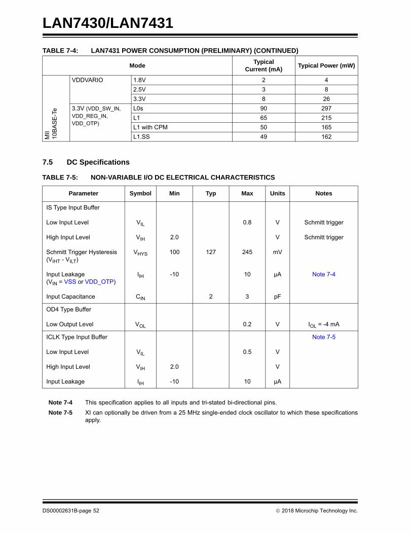
LAN7430/LAN7431
7.5 DC Specifications
Note 7-4 This specification applies to all inputs and tri-stated bi-directional pins.
Note 7-5 XI can optionally be driven from a 25 MHz single-ended clock oscillator to which these specifications apply.
MII
10B
AS
E-T
e
VDDVARIO 1.8V 2 4
2.5V 3 8
3.3V 8 26
3.3V (VDD_SW_IN,VDD_REG_IN,VDD_OTP)
L0s 90 297
L1 65 215
L1 with CPM 50 165
L1.SS 49 162
TABLE 7-5: NON-VARIABLE I/O DC ELECTRICAL CHARACTERISTICS
Parameter Symbol Min Typ Max Units Notes
IS Type Input Buffer
Low Input Level
High Input Level
Schmitt Trigger Hysteresis (VIHT - VILT)
Input Leakage(VIN = VSS or VDD_OTP)
Input Capacitance
VIL
VIH
VHYS
IIH
CIN
2.0
100
-10
127
2
0.8
245
10
3
V
V
mV
µA
pF
Schmitt trigger
Schmitt trigger
Note 7-4
OD4 Type Buffer
Low Output Level VOL 0.2 V IOL = -4 mA
ICLK Type Input Buffer
Low Input Level
High Input Level
Input Leakage
VIL
VIH
IIH
2.0
-10
0.5
10
V
V
µA
Note 7-5
TABLE 7-4: LAN7431 POWER CONSUMPTION (PRELIMINARY) (CONTINUED)
ModeTypical
Current (mA)Typical Power (mW)
DS00002631B-page 52 2018 Microchip Technology Inc.
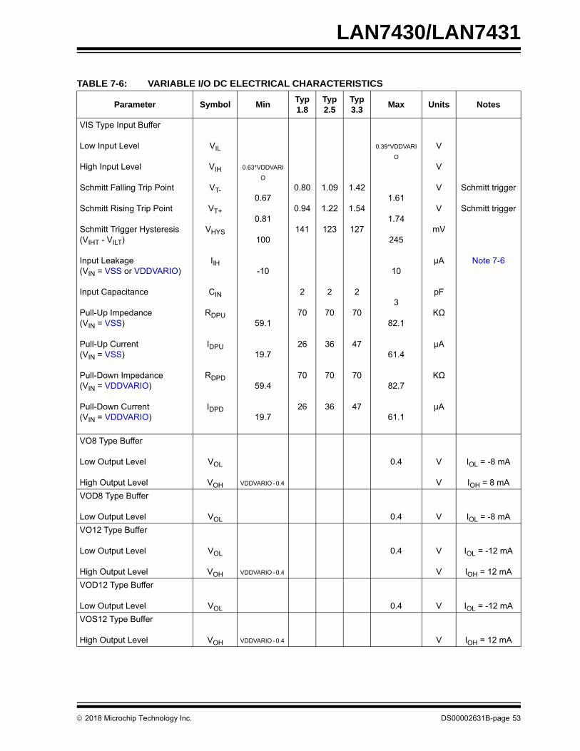
LAN7430/LAN7431
TABLE 7-6: VARIABLE I/O DC ELECTRICAL CHARACTERISTICS
Parameter Symbol MinTyp 1.8
Typ 2.5
Typ3.3
Max Units Notes
VIS Type Input Buffer
Low Input Level
High Input Level
Schmitt Falling Trip Point
Schmitt Rising Trip Point
Schmitt Trigger Hysteresis (VIHT - VILT)
Input Leakage(VIN = VSS or VDDVARIO)
Input Capacitance
Pull-Up Impedance(VIN = VSS)
Pull-Up Current(VIN = VSS)
Pull-Down Impedance(VIN = VDDVARIO)
Pull-Down Current(VIN = VDDVARIO)
VIL
VIH
VT-
VT+
VHYS
IIH
CIN
RDPU
IDPU
RDPD
IDPD
0.63*VDDVARI
O
0.67
0.81
100
-10
59.1
19.7
59.4
19.7
0.80
0.94
141
2
70
26
70
26
1.09
1.22
123
2
70
36
70
36
1.42
1.54
127
2
70
47
70
47
0.39*VDDVARI
O
1.61
1.74
245
10
3
82.1
61.4
82.7
61.1
V
V
V
V
mV
µA
pF
KΩ
µA
KΩ
µA
Schmitt trigger
Schmitt trigger
Note 7-6
VO8 Type Buffer
Low Output Level
High Output Level
VOL
VOH VDDVARIO - 0.4
0.4 V
V
IOL = -8 mA
IOH = 8 mA
VOD8 Type Buffer
Low Output Level VOL 0.4 V IOL = -8 mA
VO12 Type Buffer
Low Output Level
High Output Level
VOL
VOH VDDVARIO - 0.4
0.4 V
V
IOL = -12 mA
IOH = 12 mA
VOD12 Type Buffer
Low Output Level VOL 0.4 V IOL = -12 mA
VOS12 Type Buffer
High Output Level VOH VDDVARIO - 0.4 V IOH = 12 mA
2018 Microchip Technology Inc. DS00002631B-page 53
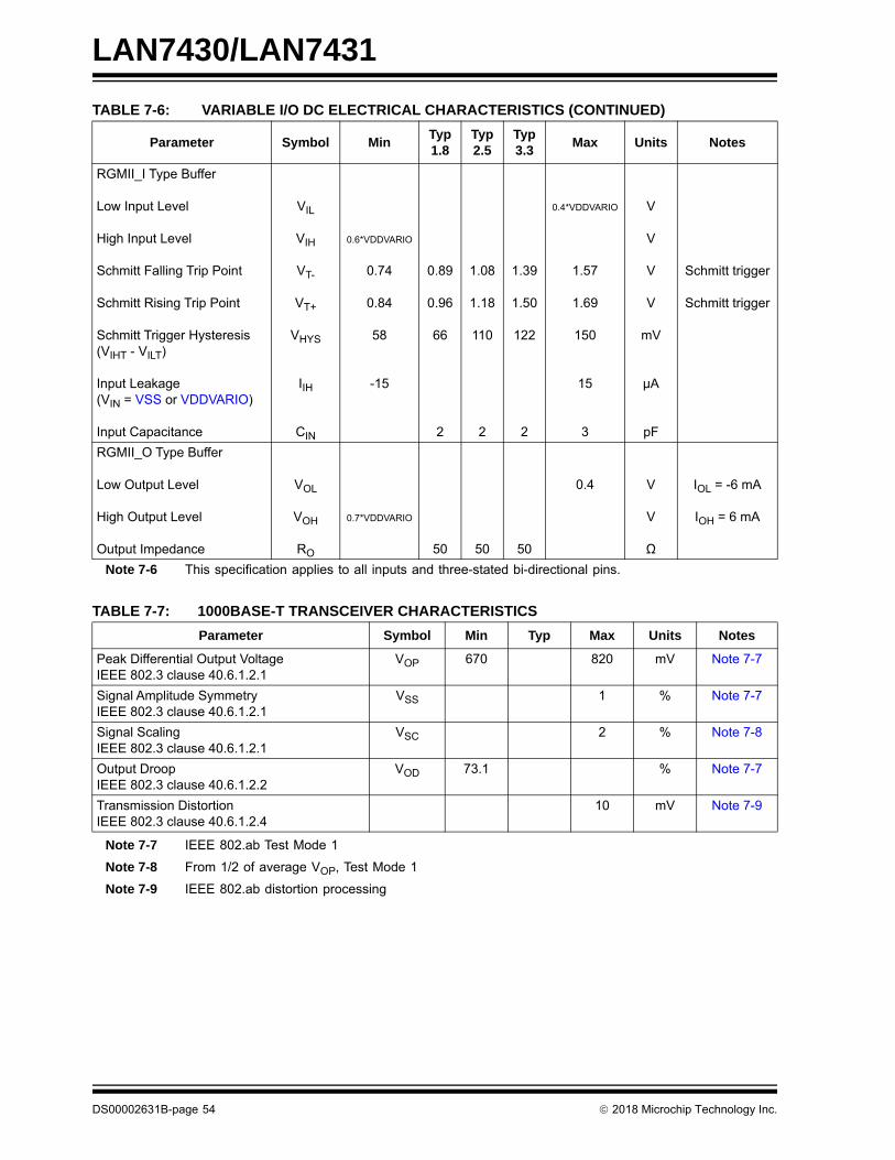
LAN7430/LAN7431
Note 7-6 This specification applies to all inputs and three-stated bi-directional pins.
Note 7-7 IEEE 802.ab Test Mode 1
Note 7-8 From 1/2 of average VOP, Test Mode 1
Note 7-9 IEEE 802.ab distortion processing
RGMII_I Type Buffer
Low Input Level
High Input Level
Schmitt Falling Trip Point
Schmitt Rising Trip Point
Schmitt Trigger Hysteresis (VIHT - VILT)
Input Leakage(VIN = VSS or VDDVARIO)
Input Capacitance
VIL
VIH
VT-
VT+
VHYS
IIH
CIN
0.6*VDDVARIO
0.74
0.84
58
-15
0.89
0.96
66
2
1.08
1.18
110
2
1.39
1.50
122
2
0.4*VDDVARIO
1.57
1.69
150
15
3
V
V
V
V
mV
µA
pF
Schmitt trigger
Schmitt trigger
RGMII_O Type Buffer
Low Output Level
High Output Level
Output Impedance
VOL
VOH
RO
0.7*VDDVARIO
50 50 50
0.4 V
V
Ω
IOL = -6 mA
IOH = 6 mA
TABLE 7-7: 1000BASE-T TRANSCEIVER CHARACTERISTICS
Parameter Symbol Min Typ Max Units Notes
Peak Differential Output VoltageIEEE 802.3 clause 40.6.1.2.1
VOP 670 820 mV Note 7-7
Signal Amplitude SymmetryIEEE 802.3 clause 40.6.1.2.1
VSS 1 % Note 7-7
Signal ScalingIEEE 802.3 clause 40.6.1.2.1
VSC 2 % Note 7-8
Output DroopIEEE 802.3 clause 40.6.1.2.2
VOD 73.1 % Note 7-7
Transmission DistortionIEEE 802.3 clause 40.6.1.2.4
10 mV Note 7-9
TABLE 7-6: VARIABLE I/O DC ELECTRICAL CHARACTERISTICS (CONTINUED)
Parameter Symbol MinTyp 1.8
Typ 2.5
Typ3.3
Max Units Notes
DS00002631B-page 54 2018 Microchip Technology Inc.

LAN7430/LAN7431
TABLE 7-8: 100BASE-TX TRANSCEIVER CHARACTERISTICS
Parameter Symbol Min Typ Max Units Notes
Peak Differential Output VoltageANSI X3.263 clause 9.1.2.2
VOUT ±0.95 - ±1.05 V Note 7-10
Signal Amplitude SymmetryANSI X3.263 clause 9.1.4
VSS - 2 % Note 7-10
Signal Rise and Fall TimeANSI X3.263 clause 9.1.6
TRF 3 - 5 nS Note 7-10
Rise and Fall SymmetryANSI X3.263 clause 9.1.6
TRFS - - 0.5 nS Note 7-10
Duty Cycle DistortionANSI X3.263 clause 9.1.8
DCD ±0.25 nS Note 7-11
Overshoot and UndershootANSI X3.263 clause 9.1.3
VOS - - 5 %
Output JitterANSI X3.263 clause 9.1.9
0.7 1.4 nS Note 7-12
Reference Voltage of ISET (using 6.04kΩ - 1% resistor)
VSET 0.65 V
Note 7-10 Measured at line side of transformer, line replaced by 100 (+/- 1%) resistor.
Note 7-11 Offset from 16nS pulse width at 50% of pulse peak.
Note 7-12 Peak to Peak, measured differentially.
Note 7-13 Min/max voltages guaranteed as measured with 100 resistive load.
Note 7-14 Measured differentially following the twisted-pair model with a 100 resistive load.
Note 7-15 5MHz square wave.
TABLE 7-9: 10BASE-T/10BASE-Te TRANSCEIVER CHARACTERISTICS
Parameter Symbol Min Typ Max Units Notes
Transmitter Peak Differential Output Volt-ageIEEE 802.3 clause 14.3.1.2.1
VOUT10BASE-T
2.2 2.5 2.8 V Note 7-13
VOUT10BASE-Te
1.54 1.96 V Note 7-13
Output JitterIEEE 802.3 clause 14.3.1.2.3
1.8 3.5 nS Note 7-14
Signal Rise and Fall Time TRF 25 nS
Receiver Differential Squelch ThresholdIEEE 802.3 clause 14.3.1.3.2
VDS 300 400 mV Note 7-15
TABLE 7-10: PCIe TRANSCEIVER CHARACTERISTICS
Parameter Symbol Min Typ Max Units Notes
Receiver Input Leakage(terminations off)
III 2 µA
Transmitter Input Leakage III 25 µA
PCIe Clock Input Leakage III 32 nA
2018 Microchip Technology Inc. DS00002631B-page 55

LAN7430/LAN7431
7.6 AC Specifications
This section details the various AC timing specifications of the device.
Note: The RGMII timing adheres to or exceeds the HP RGMII Specification Version 2.0. Refer to this specification for additional RGMII timing information.
Note: The MII timing adheres to or exceeds the IEEE 802.3 specification. Refer to the IEEE 802.3 specification for additional MII timing information.
7.6.1 EQUIVALENT TEST LOAD
Output timing specifications assume a 25pF equivalent test load, unless otherwise noted, as illustrated in Figure 7-1.
FIGURE 7-1: OUTPUT EQUIVALENT TEST LOAD
7.6.2 POWER SEQUENCE TIMING
This section details the device power sequencing requirements. The VDDVARIO, VDDVARIO_B, VDD_SW_IN, VDD_REG_IN, VDD_OTP, AVDDH_1 and AVDDH_2 power supplies must all reach operational levels within the spec-ified time period tpon, as shown in Figure 7-2. When operating with the internal regulators disabled, VDD12CORE, AVDD12, AVDDL_1, AVDDL_2, VPH, VPTX and VP are also included in this requirement, as shown in Figure 7-3.
In addition, all of the power supplies must reach 80% of their operating voltage level within 15ms. This requirement can be safely ignored if using an external reset as shown in Section 7.6.4.
Device power supplies can turn off in any order provided they all reach 0 volts within the specified time period tpoff.
FIGURE 7-2: POWER SEQUENCE TIMING (INTERNAL REGULATORS)
25 pF
OUTPUT
VDDVARIO, VDDVARIO_B
VDD_SW_IN, VDD_REG_IN, VDD_OTP, AVDDH_1, AVDDH_2
tpon tpoff
DS00002631B-page 56 2018 Microchip Technology Inc.

LAN7430/LAN7431
FIGURE 7-3: POWER SEQUENCE TIMING (EXTERNAL REGULATORS)
TABLE 7-11: POWER SEQUENCING TIMING VALUES
Symbol Description Min Typ Max Units
tpon Power supply turn on time 50 ms
tpoff Power supply turn off time 500 ms
7.6.3 POWER-ON CONFIGURATION STRAP TIMING
Figure 7-4 illustrates the configuration strap timing requirements, in relation to power-on, for applications where RESET_N is not used at power-on. The operational level (Vopp) for the external power supply is detailed in Section 7.2, "Operating Conditions**," on page 48.
FIGURE 7-4: POWER-ON CONFIGURATION STRAP TIMING
TABLE 7-12: POWER-ON CONFIGURATION STRAP TIMING
Symbol Description Min Typ Max Units
tcsh Configuration strap hold after external power supply at operational level
22 ms
todad Output drive after straps latched 3 µs
VDDVARIO, VDDVARIO_B
VDD_SW_IN, VDD_REG_IN, VDD_OTP, AVDDH_1, AVDDH_2
tpon tpoff
VDD12CORE, AVDD12, AVDDL_1, AVDDL_2, VPH, VPTX, VP
All External Power Supplies
Vopp
Configuration Strap Pins
tcsh
Output Drive
todad
2018 Microchip Technology Inc. DS00002631B-page 57
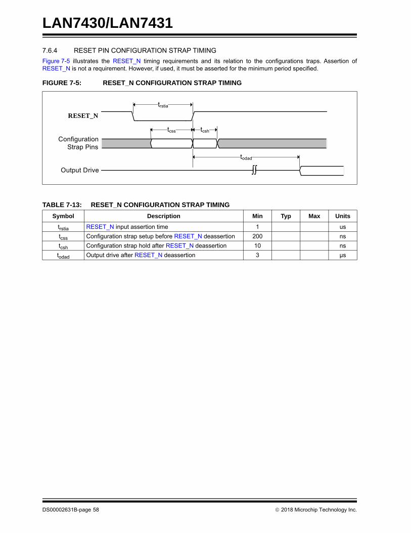
LAN7430/LAN7431
7.6.4 RESET PIN CONFIGURATION STRAP TIMING
Figure 7-5 illustrates the RESET_N timing requirements and its relation to the configurations traps. Assertion of RESET_N is not a requirement. However, if used, it must be asserted for the minimum period specified.
FIGURE 7-5: RESET_N CONFIGURATION STRAP TIMING
TABLE 7-13: RESET_N CONFIGURATION STRAP TIMING
Symbol Description Min Typ Max Units
trstia RESET_N input assertion time 1 us
tcss Configuration strap setup before RESET_N deassertion 200 ns
tcsh Configuration strap hold after RESET_N deassertion 10 ns
todad Output drive after RESET_N deassertion 3 µs
RESET_N
Configuration Strap Pins
trstia
tcshtcss
Output Drive
todad
DS00002631B-page 58 2018 Microchip Technology Inc.

LAN7430/LAN7431
7.6.5 MII TIMING (100BASE-TX, 10BASE-T) (LAN7431 ONLY)
This section specifies the LAN7431 MII interface transmit and receive timing.
TABLE 7-14: MII TRANSMIT TIMING VALUES
Symbol Description Min Max Units Notes
tclkp TX_CLK period Note 7-16 ns
tclkh TX_CLK high time tclkp*0.4 tclkp*0.6 ns
tclkl TX_CLK low time tclkp*0.4 tclkp*0.6 ns
tval TXD[3:0], TX_EN, TX_ER output valid from ris-ing edge of TX_CLK
22.0 ns Note 7-17
thold TXD[3:0], TX_EN, TX_ER output hold from ris-ing edge of TX_CLK
0 ns Note 7-17
Note 7-16 40ns for 100BASE-TX operation, 400ns for 10BASE-T operation.
Note 7-17 Timing was designed for system load between 10 pf and 25 pf.
FIGURE 7-6: MII TRANSMIT TIMING
TX_CLK
TXD[3:0], TX_ER
TX_EN
tclkh tclkl
tclkp
tval tholdtval
tval
thold
2018 Microchip Technology Inc. DS00002631B-page 59

LAN7430/LAN7431
FIGURE 7-7: MII RECEIVE TIMING
TABLE 7-15: MII RECEIVE TIMING VALUES
Symbol Description Min Max Units Notes
tclkp RX_CLK period Note 7-18 ns
tclkh RX_CLK high time tclkp*0.4 tclkp*0.6 ns
tclkl RX_CLK low time tclkp*0.4 tclkp*0.6 ns
tsu RXD[3:0], RX_DV, RX_ER setup time to rising edge of RX_CLK
8.0 ns Note 7-19
thold RXD[3:0], RX_DV, RX_ER hold time after rising edge of RX_CLK
9.0 ns Note 7-19
Note 7-18 40ns for 100BASE-TX operation, 400ns for 10BASE-T operation.
Note 7-19 Timing was designed for system load between 10 pf and 25 pf.
RX_CLK
tsu
RXD[3:0], RX_ER
RX_DV
tclkh tclkl
tclkp
thold tsu thold thold
tsuthold
DS00002631B-page 60 2018 Microchip Technology Inc.
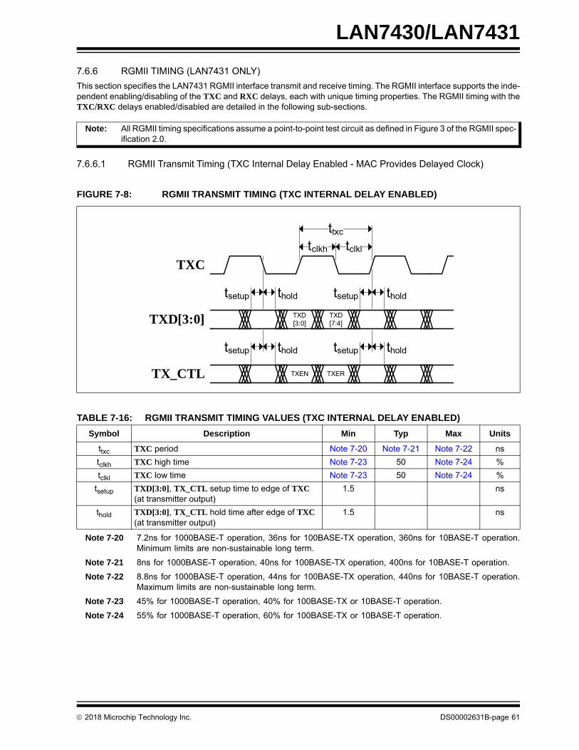
LAN7430/LAN7431
7.6.6 RGMII TIMING (LAN7431 ONLY)
This section specifies the LAN7431 RGMII interface transmit and receive timing. The RGMII interface supports the inde-pendent enabling/disabling of the TXC and RXC delays, each with unique timing properties. The RGMII timing with the TXC/RXC delays enabled/disabled are detailed in the following sub-sections.
7.6.6.1 RGMII Transmit Timing (TXC Internal Delay Enabled - MAC Provides Delayed Clock)
TABLE 7-16: RGMII TRANSMIT TIMING VALUES (TXC INTERNAL DELAY ENABLED)
Symbol Description Min Typ Max Units
ttxc TXC period Note 7-20 Note 7-21 Note 7-22 ns
tclkh TXC high time Note 7-23 50 Note 7-24 %
tclkl TXC low time Note 7-23 50 Note 7-24 %
tsetup TXD[3:0], TX_CTL setup time to edge of TXC (at transmitter output)
1.5 ns
thold TXD[3:0], TX_CTL hold time after edge of TXC (at transmitter output)
1.5 ns
Note 7-20 7.2ns for 1000BASE-T operation, 36ns for 100BASE-TX operation, 360ns for 10BASE-T operation. Minimum limits are non-sustainable long term.
Note 7-21 8ns for 1000BASE-T operation, 40ns for 100BASE-TX operation, 400ns for 10BASE-T operation.
Note 7-22 8.8ns for 1000BASE-T operation, 44ns for 100BASE-TX operation, 440ns for 10BASE-T operation. Maximum limits are non-sustainable long term.
Note 7-23 45% for 1000BASE-T operation, 40% for 100BASE-TX or 10BASE-T operation.
Note 7-24 55% for 1000BASE-T operation, 60% for 100BASE-TX or 10BASE-T operation.
Note: All RGMII timing specifications assume a point-to-point test circuit as defined in Figure 3 of the RGMII spec-ification 2.0.
FIGURE 7-8: RGMII TRANSMIT TIMING (TXC INTERNAL DELAY ENABLED)
TXC
TXD[3:0]
TX_CTL
tclkh tclkl
ttxc
TXD[3:0]
TXD[7:4]
TXEN TXER
tholdtsetup tholdtsetup
tholdtsetup tholdtsetup
2018 Microchip Technology Inc. DS00002631B-page 61
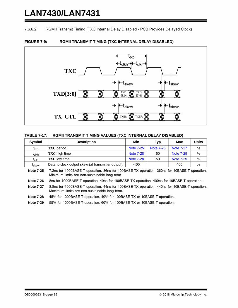
LAN7430/LAN7431
7.6.6.2 RGMII Transmit Timing (TXC Internal Delay Disabled - PCB Provides Delayed Clock)
TABLE 7-17: RGMII TRANSMIT TIMING VALUES (TXC INTERNAL DELAY DISABLED)
Symbol Description Min Typ Max Units
ttxc TXC period Note 7-25 Note 7-26 Note 7-27 ns
tclkh TXC high time Note 7-28 50 Note 7-29 %
tclkl TXC low time Note 7-28 50 Note 7-29 %
tskew Data to clock output skew (at transmitter output) -400 400 ps
Note 7-25 7.2ns for 1000BASE-T operation, 36ns for 100BASE-TX operation, 360ns for 10BASE-T operation. Minimum limits are non-sustainable long term.
Note 7-26 8ns for 1000BASE-T operation, 40ns for 100BASE-TX operation, 400ns for 10BASE-T operation.
Note 7-27 8.8ns for 1000BASE-T operation, 44ns for 100BASE-TX operation, 440ns for 10BASE-T operation. Maximum limits are non-sustainable long term.
Note 7-28 45% for 1000BASE-T operation, 40% for 100BASE-TX or 10BASE-T operation.
Note 7-29 55% for 1000BASE-T operation, 60% for 100BASE-TX or 10BASE-T operation.
FIGURE 7-9: RGMII TRANSMIT TIMING (TXC INTERNAL DELAY DISABLED)
TXC
TXD[3:0]
TX_CTL
tclkh tclkl
ttxc
TXD[3:0]
TXD[7:4]
TXEN TXER
tskew
tskew
tskew
tskew
DS00002631B-page 62 2018 Microchip Technology Inc.
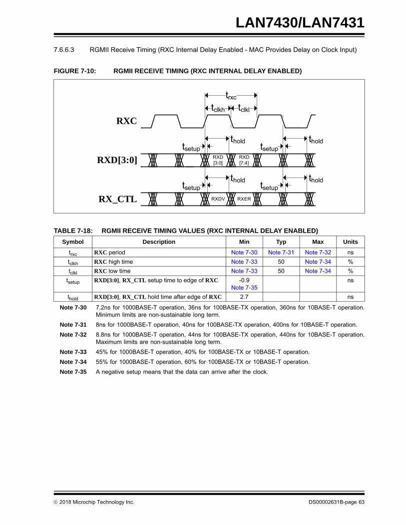
LAN7430/LAN7431
7.6.6.3 RGMII Receive Timing (RXC Internal Delay Enabled - MAC Provides Delay on Clock Input)
TABLE 7-18: RGMII RECEIVE TIMING VALUES (RXC INTERNAL DELAY ENABLED)
Symbol Description Min Typ Max Units
trxc RXC period Note 7-30 Note 7-31 Note 7-32 ns
tclkh RXC high time Note 7-33 50 Note 7-34 %
tclkl RXC low time Note 7-33 50 Note 7-34 %
tsetup RXD[3:0], RX_CTL setup time to edge of RXC -0.9Note 7-35
ns
thold RXD[3:0], RX_CTL hold time after edge of RXC 2.7 ns
Note 7-30 7.2ns for 1000BASE-T operation, 36ns for 100BASE-TX operation, 360ns for 10BASE-T operation. Minimum limits are non-sustainable long term.
Note 7-31 8ns for 1000BASE-T operation, 40ns for 100BASE-TX operation, 400ns for 10BASE-T operation.
Note 7-32 8.8ns for 1000BASE-T operation, 44ns for 100BASE-TX operation, 440ns for 10BASE-T operation. Maximum limits are non-sustainable long term.
Note 7-33 45% for 1000BASE-T operation, 40% for 100BASE-TX or 10BASE-T operation.
Note 7-34 55% for 1000BASE-T operation, 60% for 100BASE-TX or 10BASE-T operation.
Note 7-35 A negative setup means that the data can arrive after the clock.
FIGURE 7-10: RGMII RECEIVE TIMING (RXC INTERNAL DELAY ENABLED)
RXC
RXD[3:0]
RX_CTL
tclkh tclkl
trxc
RXD[3:0]
RXD[7:4]
RXDV RXER
tholdtsetup
tholdtsetup
tholdtsetup
tholdtsetup
2018 Microchip Technology Inc. DS00002631B-page 63

LAN7430/LAN7431
7.6.6.4 RGMII Receive Timing (RXC Internal Delay Disabled - PHY Provides Delayed Clock)
TABLE 7-19: RGMII RECEIVE TIMING VALUES (RXC INTERNAL DELAY DISABLED)
Symbol Description Min Typ Max Units
trxc RXC period Note 7-36 Note 7-37 Note 7-38 ns
tclkh RXC high time Note 7-39 50 Note 7-40 %
tclkl RXC low time Note 7-39 50 Note 7-40 %
tsetup RXD[3:0], RX_CTL input setup to edge of RXC 0.8 ns
thold RXD[3:0], RX_CTL input hold from edge of RXC 0.8 ns
Note 7-36 7.2ns for 1000BASE-T operation, 36ns for 100BASE-TX operation, 360ns for 10BASE-T operation. Minimum limits are non-sustainable long term.
Note 7-37 8ns for 1000BASE-T operation, 40ns for 100BASE-TX operation, 400ns for 10BASE-T operation.
Note 7-38 8.8ns for 1000BASE-T operation, 44ns for 100BASE-TX operation, 440ns for 10BASE-T operation. Maximum limits are non-sustainable long term.
Note 7-39 45% for 1000BASE-T operation, 40% for 100BASE-TX or 10BASE-T operation.
Note 7-40 55% for 1000BASE-T operation, 60% for 100BASE-TX or 10BASE-T operation.
FIGURE 7-11: RGMII RECEIVE TIMING (RXC INTERNAL DELAY DISABLED)
RXC
RXD[3:0]
RX_CTL
tclkh tclkl
trxc
RXD[3:0]
RXD[7:4]
RXDV RXER
tholdtsetup tholdtsetup
tholdtsetup tholdtsetup
DS00002631B-page 64 2018 Microchip Technology Inc.

LAN7430/LAN7431
7.6.7 MDIO INTERFACE TIMING (LAN7431 ONLY)
This section specifies the LAN7431 MDIO interface timing.
TABLE 7-20: MDIO INTERFACE TIMING VALUES
Symbol Description Min Max Units Notes
tclkp MDC period 400 ns Note 7-41
tclkh MDC high time 180 (90%) ns Note 7-41
tclkl MDC low time 180 (90%) ns Note 7-41
tval MDIO (write to PHY) output valid from rising edge of MDC
250 ns Note 7-42
tohold MDIO (write to PHY) output hold from rising edge of MDC
50 ns Note 7-42
tsu MDIO (read from PHY) input setup time to rising edge of MDC
70 ns Note 7-43
tihold MDIO (read from to PHY) input hold time after rising edge of MDC
0 ns Note 7-43
Note 7-41 The MDIO Interface outputs a nominal 400 ns clock with a 50/50 duty cycle.
Note 7-42 The MDIO Interface changes output data a nominal 120 ns following the rising edge of MDC.
Note 7-43 The MDIO Interface samples input data a nominal 40 ns prior to the rising edge of MDC.
FIGURE 7-12: MDIO INTERFACE TIMING
MDC
MDIO
tclkh tclkl
tclkp
tohold
MDIO
tsu tihold(Data-Out)
(Data-In)
tohold
tval
2018 Microchip Technology Inc. DS00002631B-page 65

LAN7430/LAN7431
7.6.8 JTAG TIMING
This section specifies the JTAG timing of the device.
TABLE 7-21: JTAG TIMING VALUES
Symbol Description Min Typ Max Units
ttckp TCK clock period 40 ns
ttckhl TCK clock high/low time ttckp*0.4 ttckp*0.6 ns
tsu TDI, TMS setup to TCK rising edge 10 ns
th TDI, TMS hold from TCK rising edge 10 ns
tdov TDO output valid from TCK falling edge 15 ns
tdoinvld TDO output invalid from TCK falling edge 0 ns
FIGURE 7-13: JTAG TIMING
Note: JTAG timing values are with respect to an equivalent test load of 25 pF.
TCK(Input)
TDI, TMS(Inputs)
ttckhl
ttckp
ttckhl
tsu th
tdov
TDO(Output)
tdohinvld
DS00002631B-page 66 2018 Microchip Technology Inc.
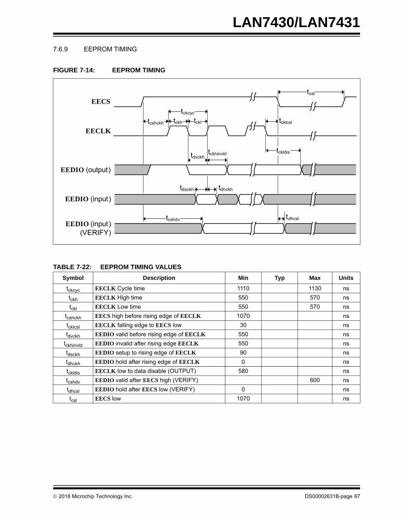
LAN7430/LAN7431
7.6.9 EEPROM TIMING
TABLE 7-22: EEPROM TIMING VALUES
Symbol Description Min Typ Max Units
tckcyc EECLK Cycle time 1110 1130 ns
tckh EECLK High time 550 570 ns
tckl EECLK Low time 550 570 ns
tcshckh EECS high before rising edge of EECLK 1070 ns
tcklcsl EECLK falling edge to EECS low 30 ns
tdvckh EEDIO valid before rising edge of EECLK 550 ns
tckhinvld EEDIO invalid after rising edge EECLK 550 ns
tdsckh EEDIO setup to rising edge of EECLK 90 ns
tdhckh EEDIO hold after rising edge of EECLK 0 ns
tckldis EECLK low to data disable (OUTPUT) 580 ns
tcshdv EEDIO valid after EECS high (VERIFY) 600 ns
tdhcsl EEDIO hold after EECS low (VERIFY) 0 ns
tcsl EECS low 1070 ns
FIGURE 7-14: EEPROM TIMING
EECLK
EEDIO (output)
EEDIO (input)
EECS
tckldis
tcshckh
EEDIO (input) (VERIFY)
tckh tckl
tckcyc
tcklcsl
tcsl
tdvckhtckhinvld
tdsckh tdhckh
tdhcsltcshdv
2018 Microchip Technology Inc. DS00002631B-page 67
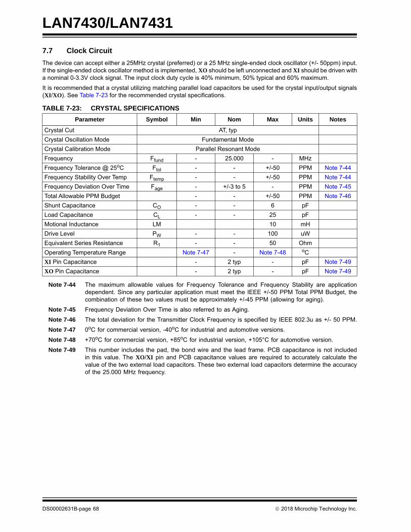
LAN7430/LAN7431
7.7 Clock Circuit
The device can accept either a 25MHz crystal (preferred) or a 25 MHz single-ended clock oscillator (+/- 50ppm) input. If the single-ended clock oscillator method is implemented, XO should be left unconnected and XI should be driven with a nominal 0-3.3V clock signal. The input clock duty cycle is 40% minimum, 50% typical and 60% maximum.
It is recommended that a crystal utilizing matching parallel load capacitors be used for the crystal input/output signals (XI/XO). See Table 7-23 for the recommended crystal specifications.
Note 7-44 The maximum allowable values for Frequency Tolerance and Frequency Stability are application dependent. Since any particular application must meet the IEEE +/-50 PPM Total PPM Budget, the combination of these two values must be approximately +/-45 PPM (allowing for aging).
Note 7-45 Frequency Deviation Over Time is also referred to as Aging.
Note 7-46 The total deviation for the Transmitter Clock Frequency is specified by IEEE 802.3u as +/- 50 PPM.
Note 7-47 0oC for commercial version, -40oC for industrial and automotive versions.
Note 7-48 +70oC for commercial version, +85oC for industrial version, +105°C for automotive version.
Note 7-49 This number includes the pad, the bond wire and the lead frame. PCB capacitance is not included in this value. The XO/XI pin and PCB capacitance values are required to accurately calculate the value of the two external load capacitors. These two external load capacitors determine the accuracy of the 25.000 MHz frequency.
TABLE 7-23: CRYSTAL SPECIFICATIONS
Parameter Symbol Min Nom Max Units Notes
Crystal Cut AT, typ
Crystal Oscillation Mode Fundamental Mode
Crystal Calibration Mode Parallel Resonant Mode
Frequency Ffund - 25.000 - MHz
Frequency Tolerance @ 25oC Ftol - - +/-50 PPM Note 7-44
Frequency Stability Over Temp Ftemp - - +/-50 PPM Note 7-44
Frequency Deviation Over Time Fage - +/-3 to 5 - PPM Note 7-45
Total Allowable PPM Budget - - +/-50 PPM Note 7-46
Shunt Capacitance CO - - 6 pF
Load Capacitance CL - - 25 pF
Motional Inductance LM 10 mH
Drive Level PW - - 100 uW
Equivalent Series Resistance R1 - - 50 Ohm
Operating Temperature Range Note 7-47 - Note 7-48 oC
XI Pin Capacitance - 2 typ - pF Note 7-49
XO Pin Capacitance - 2 typ - pF Note 7-49
DS00002631B-page 68 2018 Microchip Technology Inc.
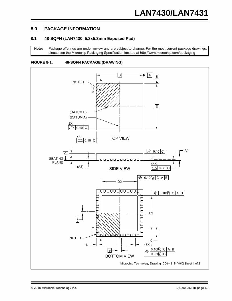
LAN7430/LAN7431
8.0 PACKAGE INFORMATION
8.1 48-SQFN (LAN7430, 5.3x5.3mm Exposed Pad)
Note: Package offerings are under review and are subject to change. For the most current package drawings, please see the Microchip Packaging Specification located at http://www.microchip.com/packaging
FIGURE 8-1: 48-SQFN PACKAGE (DRAWING)
2018 Microchip Technology Inc. DS00002631B-page 69

LAN7430/LAN7431
FIGURE 8-2: 48-SQFN PACKAGE (DIMENSIONS)
DS00002631B-page 70 2018 Microchip Technology Inc.
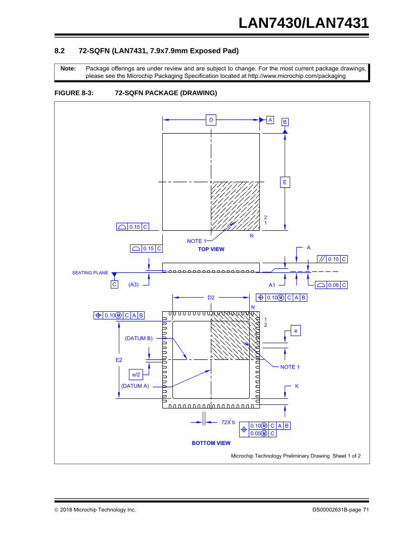
LAN7430/LAN7431
8.2 72-SQFN (LAN7431, 7.9x7.9mm Exposed Pad)
Note: Package offerings are under review and are subject to change. For the most current package drawings, please see the Microchip Packaging Specification located at http://www.microchip.com/packaging
FIGURE 8-3: 72-SQFN PACKAGE (DRAWING)
2018 Microchip Technology Inc. DS00002631B-page 71

LAN7430/LAN7431
FIGURE 8-4: 72-SQFN PACKAGE (DIMENSIONS)
DS00002631B-page 72 2018 Microchip Technology Inc.

2018 Microchip Technology Inc. DS00002631B-page 73
LAN7430/LAN7431
APPENDIX A: DATA SHEET REVISION HISTORY
TABLE A-1: REVISION HISTORY
Revision Level & Date Section/Figure/Entry Correction
DS00002631B (10-24-18) Section 6.1.2, "Reference Clock" Added the following: “PCIe architecture defines three clock distribution methods: common clock, data clock, and separate clock. The LAN7430/LAN7431 devices support the common clock method where both end devices, such as a host and the device, are using the same clock source. The details of the common clock method are provided in the PCIe specification.”
Section 3.3, "Pin Descriptions" Updated TEST pin description for clarity.
Cover, Section 2.1, "General Descrip-tion", Section 6.1, "PCI Express PHY
(PCIe PHY)"
Removed references to “IEEE 1149.6”.
Section 6.12.7, "Soft-Lite Reset" Added application note regarding LRST configuration reload.
Table 6-3, "IEEE 1149.1 Op Codes" Removed EXTEST_PULSE and EXTEST_TRAIN entries from table.
Table 7-1, "48-SQFN Package Ther-mal Parameters" and Table 7-2, "72-
SQFN Package Thermal Parameters"
Corrected JC velocity columns to indi-cate “N/A”.
Table 7-4, "LAN7431 Power Con-sumption (Preliminary)"
Corrected part number in table title.
Section 6.4, "RGMII (LAN7431 Only)" Added new section.
DS00002631A (02-09-18) All Initial Release.
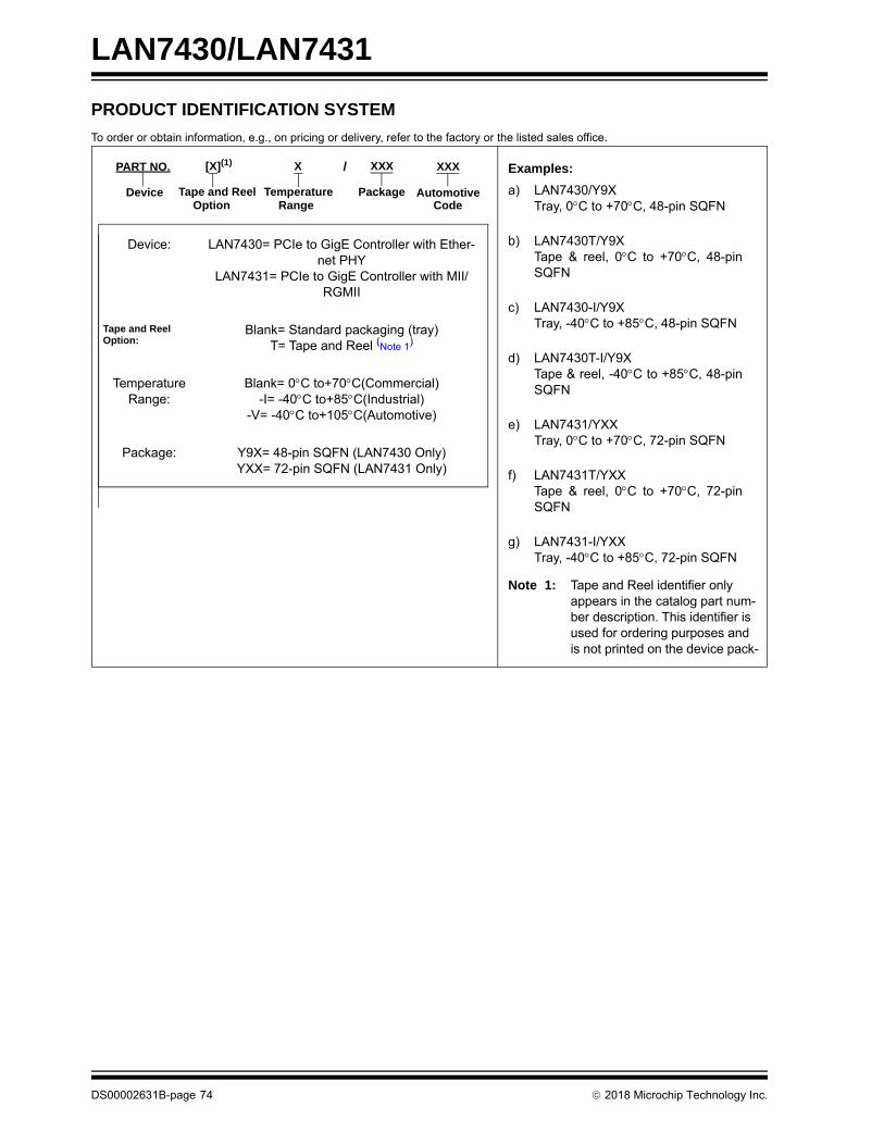
LAN7430/LAN7431
DS00002631B-page 74 2018 Microchip Technology Inc.
PRODUCT IDENTIFICATION SYSTEM
To order or obtain information, e.g., on pricing or delivery, refer to the factory or the listed sales office.
Device: LAN7430= PCIe to GigE Controller with Ether-net PHY
LAN7431= PCIe to GigE Controller with MII/RGMII
Tape and Reel Option:
Blank= Standard packaging (tray)T= Tape and Reel (Note 1)
Temperature Range:
Blank= 0C to+70C(Commercial)-I= -40C to+85C(Industrial)
-V= -40C to+105C(Automotive)
Package: Y9X= 48-pin SQFN (LAN7430 Only)YXX= 72-pin SQFN (LAN7431 Only)
Examples:
a) LAN7430/Y9XTray, 0C to +70C, 48-pin SQFN
b) LAN7430T/Y9XTape & reel, 0C to +70C, 48-pin SQFN
c) LAN7430-I/Y9XTray, -40C to +85C, 48-pin SQFN
d) LAN7430T-I/Y9XTape & reel, -40C to +85C, 48-pin SQFN
e) LAN7431/YXXTray, 0C to +70C, 72-pin SQFN
f) LAN7431T/YXXTape & reel, 0C to +70C, 72-pin SQFN
g) LAN7431-I/YXXTray, -40C to +85C, 72-pin SQFN
Note 1: Tape and Reel identifier only appears in the catalog part num-ber description. This identifier is used for ordering purposes and is not printed on the device pack-
PART NO.
Device Tape and ReelOption
/
TemperatureRange
XXX[X](1) X
Package
XXX
AutomotiveCode

2018 Microchip Technology Inc. DS00002631B-page 75
LAN7430/LAN7431
THE MICROCHIP WEB SITE
Microchip provides online support via our WWW site at www.microchip.com. This web site is used as a means to make files and information easily available to customers. Accessible by using your favorite Internet browser, the web site con-tains the following information:
• Product Support – Data sheets and errata, application notes and sample programs, design resources, user’s guides and hardware support documents, latest software releases and archived software
• General Technical Support – Frequently Asked Questions (FAQ), technical support requests, online discussion groups, Microchip consultant program member listing
• Business of Microchip – Product selector and ordering guides, latest Microchip press releases, listing of semi-nars and events, listings of Microchip sales offices, distributors and factory representatives
CUSTOMER CHANGE NOTIFICATION SERVICE
Microchip’s customer notification service helps keep customers current on Microchip products. Subscribers will receive e-mail notification whenever there are changes, updates, revisions or errata related to a specified product family or development tool of interest.
To register, access the Microchip web site at www.microchip.com. Under “Support”, click on “Customer Change Notifi-cation” and follow the registration instructions.
CUSTOMER SUPPORT
Users of Microchip products can receive assistance through several channels:
• Distributor or Representative
• Local Sales Office
• Field Application Engineer (FAE)
• Technical Support
Customers should contact their distributor, representative or field application engineer (FAE) for support. Local sales offices are also available to help customers. A listing of sales offices and locations is included in the back of this docu-ment.
Technical support is available through the web site at: http://microchip.com/support

LAN7430/LAN7431
DS
Note the following details of the code protection feature on Microchip devices:
• Microchip products meet the specification contained in their particular Microchip Data Sheet.
• Microchip believes that its family of products is one of the most secure families of its kind on the market today, when used in the intended manner and under normal conditions.
• There are dishonest and possibly illegal methods used to breach the code protection feature. All of these methods, to our knowledge, require using the Microchip products in a manner outside the operating specifications contained in Microchip’s Data Sheets. Most likely, the person doing so is engaged in theft of intellectual property.
• Microchip is willing to work with the customer who is concerned about the integrity of their code.
• Neither Microchip nor any other semiconductor manufacturer can guarantee the security of their code. Code protection does not mean that we are guaranteeing the product as “unbreakable.”
Code protection is constantly evolving. We at Microchip are committed to continuously improving the code protection features of our products. Attempts to break Microchip’s code protection feature may be a violation of the Digital Millennium Copyright Act. If such acts allow unauthorized access to your software or other copyrighted work, you may have a right to sue for relief under that Act.
Information contained in this publication regarding device applications and the like is provided only for your convenience and may be superseded by updates. It is your responsibility to ensure that your application meets with your specifications. MICROCHIP MAKES NO REPRESENTATIONS OR WARRANTIES OF ANY KIND WHETHER EXPRESS OR IMPLIED, WRITTEN OR ORAL, STATUTORY OR OTHERWISE, RELATED TO THE INFORMATION, INCLUDING BUT NOT LIMITED TO ITS CONDITION, QUALITY, PERFORMANCE, MERCHANTABILITY OR FITNESS FOR PURPOSE. Microchip disclaims all liability arising from this information and its use. Use of Micro-chip devices in life support and/or safety applications is entirely at the buyer’s risk, and the buyer agrees to defend, indemnify and hold harmless Microchip from any and all damages, claims, suits, or expenses resulting from such use. No licenses are conveyed, implicitly or otherwise, under any Microchip intellectual property rights unless otherwise stated.
Trademarks
The Microchip name and logo, the Microchip logo, AnyRate, AVR, AVR logo, AVR Freaks, BitCloud, chipKIT, chipKIT logo, CryptoMemory, CryptoRF, dsPIC, FlashFlex, flexPWR, Heldo, JukeBlox, KeeLoq, Kleer, LANCheck, LINK MD, maXStylus, maXTouch, MediaLB, megaAVR, MOST, MOST logo, MPLAB, OptoLyzer, PIC, picoPower, PICSTART, PIC32 logo, Prochip Designer, QTouch, SAM-BA, SpyNIC, SST, SST Logo, SuperFlash, tinyAVR, UNI/O, and XMEGA are registered trademarks of Microchip Technology Incorporated in the U.S.A. and other countries.
ClockWorks, The Embedded Control Solutions Company, EtherSynch, Hyper Speed Control, HyperLight Load, IntelliMOS, mTouch, Precision Edge, and Quiet-Wire are registered trademarks of Microchip Technology Incorporated in the U.S.A.
Adjacent Key Suppression, AKS, Analog-for-the-Digital Age, Any Capacitor, AnyIn, AnyOut, BodyCom, CodeGuard, CryptoAuthentication, CryptoAutomotive, CryptoCompanion, CryptoController, dsPICDEM, dsPICDEM.net, Dynamic Average Matching, DAM, ECAN, EtherGREEN, In-Circuit Serial Programming, ICSP, INICnet, Inter-Chip Connectivity, JitterBlocker, KleerNet, KleerNet logo, memBrain, Mindi, MiWi, motorBench, MPASM, MPF, MPLAB Certified logo, MPLIB, MPLINK, MultiTRAK, NetDetach, Omniscient Code Generation, PICDEM, PICDEM.net, PICkit, PICtail, PowerSmart, PureSilicon, QMatrix, REAL ICE, Ripple Blocker, SAM-ICE, Serial Quad I/O, SMART-I.S., SQI, SuperSwitcher, SuperSwitcher II, Total Endurance, TSHARC, USBCheck, VariSense, ViewSpan, WiperLock, Wireless DNA, and ZENA are trademarks of Microchip Technology Incorporated in the U.S.A. and other countries.
SQTP is a service mark of Microchip Technology Incorporated in the U.S.A.
Silicon Storage Technology is a registered trademark of Microchip Technology Inc. in other countries.
GestIC is a registered trademark of Microchip Technology Germany II GmbH & Co. KG, a subsidiary of Microchip Technology Inc., in other countries.
All other trademarks mentioned herein are property of their respective companies.
© 2018, Microchip Technology Incorporated, All Rights Reserved.
ISBN: 9781522436256
00002631B-page 76 2018 Microchip Technology Inc.
Microchip received ISO/TS-16949:2009 certification for its worldwide headquarters, design and wafer fabrication facilities in Chandler and Tempe, Arizona; Gresham, Oregon and design centers in California and India. The Company’s quality system processes and procedures are for its PIC® MCUs and dsPIC® DSCs, KEELOQ® code hopping devices, Serial EEPROMs, microperipherals, nonvolatile memory and analog products. In addition, Microchip’s quality system for the design and manufacture of development systems is ISO 9001:2000 certified.
QUALITYMANAGEMENTSYSTEMCERTIFIEDBYDNV
== ISO/TS16949==

2018 Microchip Technology Inc. DS00002631B-page 77
AMERICASCorporate Office2355 West Chandler Blvd.Chandler, AZ 85224-6199Tel: 480-792-7200 Fax: 480-792-7277Technical Support: http://www.microchip.com/supportWeb Address: www.microchip.com
AtlantaDuluth, GA Tel: 678-957-9614 Fax: 678-957-1455
Austin, TXTel: 512-257-3370
BostonWestborough, MA Tel: 774-760-0087 Fax: 774-760-0088
ChicagoItasca, IL Tel: 630-285-0071 Fax: 630-285-0075
DallasAddison, TX Tel: 972-818-7423 Fax: 972-818-2924
DetroitNovi, MI Tel: 248-848-4000
Houston, TX Tel: 281-894-5983
IndianapolisNoblesville, IN Tel: 317-773-8323Fax: 317-773-5453Tel: 317-536-2380
Los AngelesMission Viejo, CA Tel: 949-462-9523Fax: 949-462-9608Tel: 951-273-7800
Raleigh, NC Tel: 919-844-7510
New York, NY Tel: 631-435-6000
San Jose, CA Tel: 408-735-9110Tel: 408-436-4270
Canada - TorontoTel: 905-695-1980 Fax: 905-695-2078
ASIA/PACIFICAustralia - SydneyTel: 61-2-9868-6733
China - BeijingTel: 86-10-8569-7000
China - ChengduTel: 86-28-8665-5511
China - ChongqingTel: 86-23-8980-9588
China - DongguanTel: 86-769-8702-9880
China - GuangzhouTel: 86-20-8755-8029
China - HangzhouTel: 86-571-8792-8115
China - Hong Kong SARTel: 852-2943-5100
China - NanjingTel: 86-25-8473-2460
China - QingdaoTel: 86-532-8502-7355
China - ShanghaiTel: 86-21-3326-8000
China - ShenyangTel: 86-24-2334-2829
China - ShenzhenTel: 86-755-8864-2200
China - SuzhouTel: 86-186-6233-1526
China - WuhanTel: 86-27-5980-5300
China - XianTel: 86-29-8833-7252
China - XiamenTel: 86-592-2388138
China - ZhuhaiTel: 86-756-3210040
ASIA/PACIFICIndia - BangaloreTel: 91-80-3090-4444
India - New DelhiTel: 91-11-4160-8631
India - PuneTel: 91-20-4121-0141
Japan - OsakaTel: 81-6-6152-7160
Japan - TokyoTel: 81-3-6880- 3770
Korea - DaeguTel: 82-53-744-4301
Korea - SeoulTel: 82-2-554-7200
Malaysia - Kuala LumpurTel: 60-3-7651-7906
Malaysia - PenangTel: 60-4-227-8870
Philippines - ManilaTel: 63-2-634-9065
SingaporeTel: 65-6334-8870
Taiwan - Hsin ChuTel: 886-3-577-8366
Taiwan - KaohsiungTel: 886-7-213-7830
Taiwan - TaipeiTel: 886-2-2508-8600
Thailand - BangkokTel: 66-2-694-1351
Vietnam - Ho Chi MinhTel: 84-28-5448-2100
EUROPEAustria - WelsTel: 43-7242-2244-39Fax: 43-7242-2244-393
Denmark - CopenhagenTel: 45-4450-2828 Fax: 45-4485-2829
Finland - EspooTel: 358-9-4520-820
France - ParisTel: 33-1-69-53-63-20 Fax: 33-1-69-30-90-79
Germany - GarchingTel: 49-8931-9700
Germany - HaanTel: 49-2129-3766400
Germany - HeilbronnTel: 49-7131-67-3636
Germany - KarlsruheTel: 49-721-625370
Germany - MunichTel: 49-89-627-144-0 Fax: 49-89-627-144-44
Germany - RosenheimTel: 49-8031-354-560
Israel - Ra’anana Tel: 972-9-744-7705
Italy - Milan Tel: 39-0331-742611 Fax: 39-0331-466781
Italy - PadovaTel: 39-049-7625286
Netherlands - DrunenTel: 31-416-690399 Fax: 31-416-690340
Norway - TrondheimTel: 47-7288-4388
Poland - WarsawTel: 48-22-3325737
Romania - BucharestTel: 40-21-407-87-50
Spain - MadridTel: 34-91-708-08-90Fax: 34-91-708-08-91
Sweden - GothenbergTel: 46-31-704-60-40
Sweden - StockholmTel: 46-8-5090-4654
UK - WokinghamTel: 44-118-921-5800Fax: 44-118-921-5820
Worldwide Sales and Service
08/15/18