Laboratory Serial Finite Impulse Response...
27
Laboratory Serial Finite Impulse Response Filter Team: Chao Chen, Bing Li, Chao Wang Reporter: Chao Chen Hand-In Date: 16.July.2003 Assistant: Dipl. µ Ing. Palme Lecture: DSP with FPGAs Supervisor: Prof. Dr. B. Schwarz
Transcript of Laboratory Serial Finite Impulse Response...

Laboratory Serial Finite Impulse Response Filter
Team: Chao Chen, Bing Li, Chao Wang Reporter: Chao Chen
Hand-In Date: 16.July.2003 Assistant: Dipl. µ Ing. Palme
Lecture: DSP with FPGAs
Supervisor: Prof. Dr. B. Schwarz

Index
I. Laboratory Task Description.................................................................................... 1 II. Introduction, FIR Theory and Matlab Pre-estimation .............................................. 2 III. FIR Implementation Structure .................................................................................. 5
Timing Diagram ........................................................................................................... 7 FSM State Diagram ...................................................................................................... 9
IV. Simplified FPGA Implementation Analysis .......................................................... 10 V. Check of Final Result with Frequency Analyzer.................................................... 11
1. Group Delay ....................................................................................................... 11 2. Codec Frequency Response................................................................................ 12 3. 64th FIR Filter Frequency Response................................................................... 12
VI. Appendix ................................................................................................................ 13 Appendix 1. Matlab Pre-Calculation .......................................................................... 13 Appendix 2. Lising of Filter Coefficients................................................................... 15 Appendix 3. MAC Unit Source Code......................................................................... 17 Appendix 4. Source Code for Generating Telegramms in the Simulation................. 19 Appendix 5. Source Code for Converting Decimal Number into Binary Number .... 22 Appendix 6. VHDL Source Code Hierarchical Structure .......................................... 24

Serial FIR Filter Laboratory DSP with FPGA
Page 1
I. Laboratory Task Description A FIR filter with MAC unit, Sample and Coefficient Block-RAM is to be implemented with the FPGA-Codec platform. The FIR should fulfil the following parameter criterions from the specification.
1) Low-pass filter with order N=64. 2) Sample width 12 bits and coefficient width 12 bit. Both sample and coefficient
should be implemented with synchronous clocked Block SelectRAM memory in Spartan II.
3) The Spartan II system clock is 24MHz and the Codec interface needs a 12MHz
clock to drive it. Therefore Delay-Locked-Loop (DLL) module has to be instantiated in order to provide a clock frequency divider.
4) The Codec interface is provided by Prof. B. Schwarz to simplify and speed up
the development.
5) The filter implementation has to be checked with a frequency response analyser
and the results have to be compared with frequency response calculations from the Matlab.
6) A DIP switch can be used to switch between direct input-output without filter
operation and FIR filter function.

Serial FIR Filter Laboratory DSP with FPGA
Page 2
II. Introduction, FIR Theory and Matlab Pre-estimation Digital filters are typically used to modify or alter the attributes of a signal in the time or frequency domain. The most common digital filter is the linear time invariant (LTI) filter. An LTI interacts with its input signal through a process called linear convolution, denoted by Y = H * X where H is the filter“s impulse response (or filter kernel), X is the input signal and Y is the convolved output. The linear convolution process is formally defined by:
∑=
−==N
kknnkxnhnxny
0
][][][*][][ (Eq-1)
LTI digital filters are generally classified as being finite impulse response (FIR), or infinite impulse response (IIR). An FIR filter consists of a finite number of sample values and each output is excited by each new input signal. An IIR filter requires that an infinite sum to be performed, i.e., it remembers the past of the output. The infinite output signal duration is caused by the feedback of stored y[n] results which influence itself again with each calculation. The motivation for discussing digital filters is found in their growing popularity. Digital filters are rapidly replacing classic analog filters, which were implemented using RLC components and operational amplifiers. Analog filters were mathematically modelled using ordinary differential equations of Laplace transforms. They were analyzed in the time or s domain. Analog prototypes are now only used in IIR design, while FIR are typically designed using direct computer specifications and algorithms. In this laboratory exercise we focus on the FIR filter in particular. An Nth order FIR filter is graphically interpreted in Figure 1. It can be seen to consist of a collection of a ” tapped delay line„ adders and multipliers. One of the operands presented to each multiplier is an FIR coefficient, often referred to as a ” tap weight„. The FIR filter is also known by the name ” transversal filter„, suggesting its ” tapped delay line„ structure.
Z-1 Z-1 Z-1 Z-1 Z-1 Z-1
C0 C1 C2 C3 C4 C5 C6
+ + + + + +
X[n]
Y[n]
Figure 1. FIR Block Diagram (e.g. Order N = 6)
Maintaining phase integrity across a range of frequencies is a desired system attribute in many applications. As a result, designing filters that establish linear-phase versus frequency is often mandatory. The standard measure of the phase linearity of a system is the ”group delay„ define by:
ωω
τdHd
gr)(∠
−= (Eq-2)

Serial FIR Filter Laboratory DSP with FPGA
Page 3
A perfectly linear-phase filter has a group delay that is constant over range of frequencies. It can be shown that linear-phase is achieved if the filter is symmetric or anti-symmetric. Consider an order N=64 FIR filter design with a rectangular window (Figure 2) with the passband ripple (Figure 3 upper). Notice that the filter provides a reasonable approximation to the ideal lowpass filter with the greatest mismatch occurring at the edges of the transition band. The observed ” ringing„ is due to Gibbs phenomenon. The effects of ringing can only be suppressed with the use of a ”window„ which changes smoothly to zero on both sides, which results in a smoother magnitude frequency response with an attendant widening of the transition band. This is the trade-off. In our case, a Hamming window (Figure 4) is applied to the FIR (Figure 5), the Gibbs ringing can be reduced as shown in Figure 6.
-40 -30 -20 -10 0 10 20 30 40-0.2
-0.1
0
0.1
0.2
0.3
0.4
0.5Sampled Impulse Response
Sample Number
Am
plitu
de
Figure 2. Sampled impulse response of rectangular window
0 0.5 1 1.5 2
x 104
-100
-50
0
50
Frequency (Hz)
Mag
nitu
de (d
B)
0 0.5 1 1.5 2
x 104
-3000
-2000
-1000
0
Frequency (Hz)
Pha
se (d
egre
es)
Figure 3. Frequency response applying rectangular window

Serial FIR Filter Laboratory DSP with FPGA
Page 4
0 10 20 30 40 50 60 700
0.1
0.2
0.3
0.4
0.5
0.6
0.7
0.8
0.9
1Hamming window
Sample number
Val
ue
Figure 4. Hamming window
0 10 20 30 40 50 60-0.2
-0.1
0
0.1
0.2
0.3
0.4
0.5FIR filter coefficients with Hamm window
Number
Val
ue
Figure 5. Sampled impulse response of Hamming window
The 3 dB bandwidth is the bandwidth where the transfer function is decreased form DC by 3 dB. Hamming window also generates sidelobes but the attenuation is much higher compared to rectangular window. (Figure 6)
0 0.1 0.2 0.3 0.4 0.5 0.6 0.7 0.8 0.9 1-150
-100
-50
0
50
Normalized Angular Frequency (×π rads/sample)
Mag
nitu
de (d
B)
0 0.1 0.2 0.3 0.4 0.5 0.6 0.7 0.8 0.9 1-4000
-3000
-2000
-1000
0
Normalized Angular Frequency (×π rads/sample)
Pha
se (d
egre
es)
Figure 6. Frequency response applying Hamming window
Serial FIR Filter Laboratory DSP with FPGA
Page 5
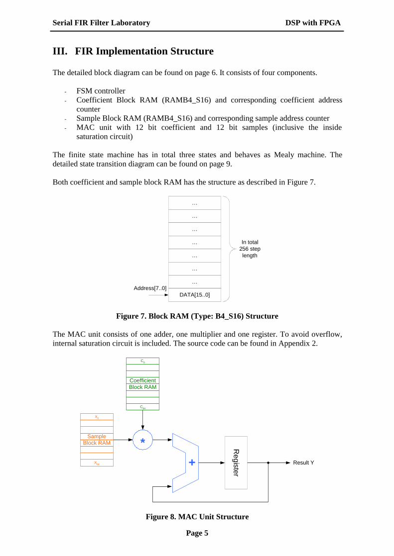
III. FIR Implementation Structure The detailed block diagram can be found on page 6. It consists of four components.
- FSM controller - Coefficient Block RAM (RAMB4_S16) and corresponding coefficient address
counter - Sample Block RAM (RAMB4_S16) and corresponding sample address counter - MAC unit with 12 bit coefficient and 12 bit samples (inclusive the inside
saturation circuit) The finite state machine has in total three states and behaves as Mealy machine. The detailed state transition diagram can be found on page 9. Both coefficient and sample block RAM has the structure as described in Figure 7.
´
´
´
´
´
´
´
DATA[15..0]
In total256 steplength
Address[7..0]
Figure 7. Block RAM (Type: B4_S16) Structure The MAC unit consists of one adder, one multiplier and one register. To avoid overflow, internal saturation circuit is included. The source code can be found in Appendix 2.
+* R
egister
CoefficientBlock RAM
SampleBlock RAM
C0
C64
X0
X64 Result Y
Figure 8. MAC Unit Structure

Page 6
FSM_FIR
ADR_CNT_SAMP
RAM_SAMP
MPY
ADD REG
SAT
ADR_CNT_COEF
RAM_COEF
ADC_FULL_IP
CLK_IP
WE_RAM_SAMP_OP
EN_ADR_CNT_SAMP_OP
ADR_CNT_COEF_ZERO_IP
ADC_FULL
CLK
RESET
RESET_IP
EN_ADR_CNT_COEF_OP EN_IP
ZERO_OP
ADR_IPVADR_COEF_OPV
WE_IP
RESET_IP
DI_IPV
EN_IP`1�
8
CLK_IP RESET_IP
CLK_IP
DO_OPV
16CLR_REG
_OP
EN_REG_OP
I: InputO: OutputP: PortS: SignalV: Vector
ADR: AddressCOEF: CoefficientCNT: CounterMPY: MultiplierPROD: ProductSAMP: SampleWE: Write Enable
Abbreviation List:
µ Figured by Chao Chen08.April.2003
Serial FIR Filter Block Structure Diagram
RESET_IP
CLK_IPEN_IP
8ADR_SAMP_OPV
ADR_IPV
WE_IP
RESET_IP
DI_IPV
EN_IP
CLK_IP
DO_OPV
`1�
X20 16
0000 & X(19 .. 8)
SAMP(11 .. 0)16 12
COEF(11 .. 0)
SAMP_IPV
COEF_IPV 12
Y20
RESET_IP CLK_IPCLR_IP EN_IPPROD_OPV
24 A_SV
B_SV
30 30ADD_SV Y_SV
Y_OPV
20
Lecture: DSP with FPGAProf. Dr. B. Schwarz
SAMP: Sample WE: Write Enable
Figure 9.
Serial FIR Filter Laboratory DSP with FPGA
Page 7
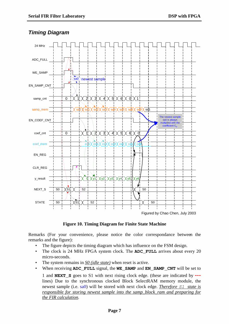
Timing Diagram
ADC_FULL
WE_SAMP
EN_SAMP_CNT
samp_cnt
EN_COEF_CNT
coef_cnt
EN_REG
CLR_REG
NEXT_S
STATE
0 1 2 3 4 5 6 0 1
0 1 2 3 4 5 6 0
S0 S1 S2 S0
S0 S1 S2 S0
samp_mem
coef_mem
sa1 sa2 sa3 sa4 sa5 sa6 sa0 sa1
co5 co4 co3 co2 co1 co0co6
y_result y1 y2 y3 y4 y5 y60
24 MHz
sa0
Figured by Chao Chen, July 2003
sa0
newest sample
The newest samplesa0 is always
multiplied with thecoefficient C0.
Figure 10. Timing Diagram for Finite State Machine Remarks (For your convenience, please notice the color correspondance between the remarks and the figure):
• The figure depicts the timing diagram which has influence on the FSM design. • The clock is 24 MHz FPGA system clock. The ADC_FULL arrives about every 20
micro-seconds. • The system remains in S0 (idle state) when reset is active. • When receiving ADC_FULL signal, the WE_SAMP and EN_SAMP_CNT will be set to
1 and NEXT_S goes to S1 with next rising clock edge. (these are indicated by --- lines) Due to the synchronous clocked Block SelectRAM memory module, the newest sample (i.e. sa0) will be stored with next clock edge. Therefore S1 state is responsible for storing newest sample into the samp_block_ram and preparing for the FIR calculation.
Serial FIR Filter Laboratory DSP with FPGA
Page 8
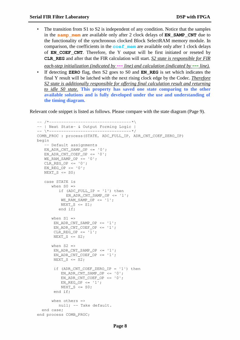
• The transition from S1 to S2 is independent of any condition. Notice that the samples in the samp_mem are available only after 2 clock delays of EN_SAMP_CNT due to the functionality of the synchronous clocked Block SelectRAM memory module. In comparison, the coefficients in the coef_mem are available only after 1 clock delays of EN_COEF_CNT. Therefore, the Y output will be first initiated or reseted by CLR_REG and after that the FIR calculation will start. S2 state is responsible for FIR each-step initialization (indicated by --- line) and calculation (indicated by --- line).
• If detecting ZERO flag, then S2 goes to S0 and EN_REG is set which indicates the final Y result will be latched with the next rising clock edge by the Codec. Therefore S2 state is additionally responsible for offering final calculation result and returning to idle S0 state. This property has saved one state comparing to the other available solutions and is fully developed under the use and understanding of the timing diagram.
Relevant code snippet is listed as follows. Please compare with the state diagram (Page 9). -- /*----------------------------------*\ -- | Next State- & Output Forming Logic | -- \*----------------------------------*/ COMB_PROC : process(STATE, ADC_FULL_IP, ADR_CNT_COEF_ZERO_IP) begin -- Default assignments EN_ADR_CNT_SAMP_OP <= '0'; EN_ADR_CNT_COEF_OP <= '0'; WE_RAM_SAMP_OP <= '0'; CLR_REG_OP <= '0'; EN_REG_OP <= '0'; NEXT_S <= S0; case STATE is when S0 => if (ADC_FULL_IP = '1') then EN_ADR_CNT_SAMP_OP <= '1'; WE_RAM_SAMP_OP <= '1'; NEXT_S <= S1; end if; when S1 => EN_ADR_CNT_SAMP_OP <= '1'; EN_ADR_CNT_COEF_OP <= '1'; CLR_REG_OP <= '1'; NEXT_S <= S2; when S2 => EN_ADR_CNT_SAMP_OP <= '1'; EN_ADR_CNT_COEF_OP <= '1'; NEXT_S <= S2; if (ADR_CNT_COEF_ZERO_IP = '1') then EN_ADR_CNT_SAMP_OP <= '0'; EN_ADR_CNT_COEF_OP <= '0'; EN_REG_OP <= '1'; NEXT_S <= S0; end if; when others => null; -- Take default. end case; end process COMB_PROC;

Serial FIR Filter Laboratory DSP with FPGA
Page 9
FSM State Diagram
S2
S0 S1
Reset
1X/110000X/00000
XX/01101
0X/01100
X1/00010
Sx
ADC_FULL, Zero /WE_SAMP,
EN_SAMP_CNT,EN_COEF_CNT,
EN_REG,CLR_REG
Serial FIR Filter Laboratory DSP with FPGA
Page 10
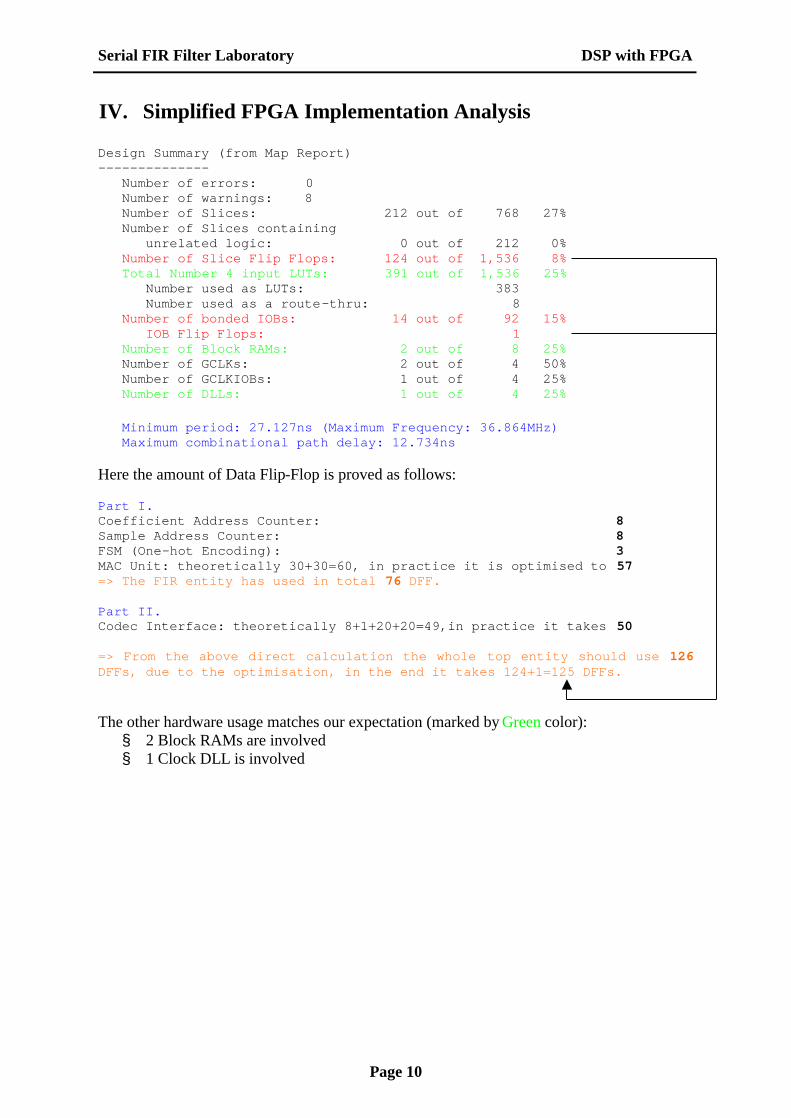
IV. Simplified FPGA Implementation Analysis Design Summary (from Map Report) -------------- Number of errors: 0 Number of warnings: 8 Number of Slices: 212 out of 768 27% Number of Slices containing unrelated logic: 0 out of 212 0% Number of Slice Flip Flops: 124 out of 1,536 8% Total Number 4 input LUTs: 391 out of 1,536 25% Number used as LUTs: 383 Number used as a route-thru: 8 Number of bonded IOBs: 14 out of 92 15% IOB Flip Flops: 1 Number of Block RAMs: 2 out of 8 25% Number of GCLKs: 2 out of 4 50% Number of GCLKIOBs: 1 out of 4 25% Number of DLLs: 1 out of 4 25% Minimum period: 27.127ns (Maximum Frequency: 36.864MHz) Maximum combinational path delay: 12.734ns Here the amount of Data Flip-Flop is proved as follows: Part I. Coefficient Address Counter: 8 Sample Address Counter: 8 FSM (One-hot Encoding): 3 MAC Unit: theoretically 30+30=60, in practice it is optimised to 57 => The FIR entity has used in total 76 DFF. Part II. Codec Interface: theoretically 8+1+20+20=49,in practice it takes 50 => From the above direct calculation the whole top entity should use 126 DFFs, due to the optimisation, in the end it takes 124+1=125 DFFs. The other hardware usage matches our expectation (marked by Green color): § 2 Block RAMs are involved § 1 Clock DLL is involved
Serial FIR Filter Laboratory DSP with FPGA
Page 11
Input rectangular
Output going through Codec
V. Check of Final Result with Frequency Analyzer
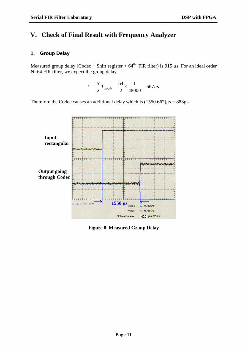
1. Group Delay Measured group delay (Codec + Shift register + 64th FIR filter) is 915 –s. For an ideal order N=64 FIR filter, we expect the group delay
sTNsample µτ 667
480001
264
2=×==
Therefore the Codec causes an additional delay which is (1550-667)–s = 883–s.
Figure 8. Measured Group Delay
1550 � s
420

Serial FIR Filter Laboratory DSP with FPGA
Page 12
2. Codec Frequency Response The Codec self has its own cut-off frequency at 22.016 kHz. Due to some technical tuning reason, -28.490 dB represents 0 dB in reality.
Figure 9. Codec Frequency Response
3. 64th FIR Filter Frequency Response The 64th FIR filter meets its specifications: cut-off frequency is 12.008 kHz, stopband attenuation reaches �50 dB ~ �60 dB.
Figure 10. 64th FIR Filter Frequency Response
22.016 kHz, -28.490 dB
12.008 kHz, -28.202 dB
Serial FIR Filter Laboratory DSP with FPGA
Page 13
VI. Appendix
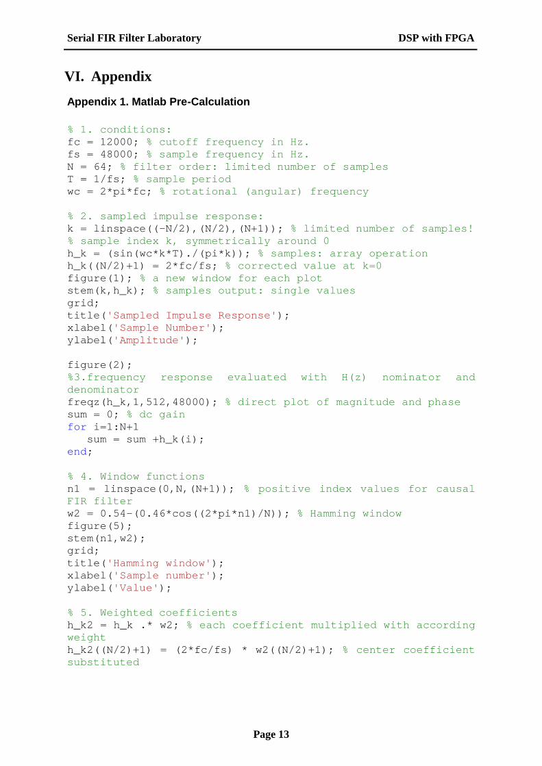
Appendix 1. Matlab Pre-Calculation % 1. conditions: fc = 12000; % cutoff frequency in Hz. fs = 48000; % sample frequency in Hz. N = 64; % filter order: limited number of samples T = 1/fs; % sample period wc = 2*pi*fc; % rotational (angular) frequency % 2. sampled impulse response: k = linspace((-N/2),(N/2),(N+1)); % limited number of samples! % sample index k, symmetrically around 0 h_k = (sin(wc*k*T)./(pi*k)); % samples: array operation h_k((N/2)+1) = 2*fc/fs; % corrected value at k=0 figure(1); % a new window for each plot stem(k,h_k); % samples output: single values grid; title('Sampled Impulse Response'); xlabel('Sample Number'); ylabel('Amplitude'); figure(2); %3.frequency response evaluated with H(z) nominator and denominator freqz(h_k,1,512,48000); % direct plot of magnitude and phase sum = 0; % dc gain for i=1:N+1 sum = sum +h_k(i); end; % 4. Window functions n1 = linspace(0,N,(N+1)); % positive index values for causal FIR filter w2 = 0.54-(0.46*cos((2*pi*n1)/N)); % Hamming window figure(5); stem(n1,w2); grid; title('Hamming window'); xlabel('Sample number'); ylabel('Value'); % 5. Weighted coefficients h_k2 = h_k .* w2; % each coefficient multiplied with according weight h_k2((N/2)+1) = (2*fc/fs) * w2((N/2)+1); % center coefficient substituted

Serial FIR Filter Laboratory DSP with FPGA
Page 14
% 6. Plots of weighted coefficients figure(6); stem(n1,h_k2); grid; title('FIR filter coefficients with Hamm window'); xlabel('Number'); ylabel('Value'); axis([(0) (N) -.2 .5]); sum2 = 0; % dc gain for i=1:N+1 sum2 = sum2 +h_k2(i); end; fHz = linspace(0,fs,(fs/10)+1); fHz0 = (2*fHz)./fs; omega = 2*pi*fHz; z = exp(sqrt(-1) * omega / fs); % 7. frequency response direct display figure(7); freqz(h_k2,1); % Evaluation of |H(w)| hw02 = abs(polyval(h_k2,z)); % Hamming hw2 = 20*log10(hw02); figure(8); plot(fHz0,hw2); grid; title('Frequency Response with Hamm window'); xlabel('Frequency scaled f/(fs/2)'); ylabel('Magnitude/dB'); axis([0.0 1.0 -80 (max(hw2)+2)]);

Serial FIR Filter Laboratory DSP with FPGA
Page 15
Appendix 2. Lising of Filter Coefficients Accurate 16-bit Q-Format 12-bit rounded Hex Rebuilt floating Floating point representation Q-Format display point coefficients coefficients of 1st Column representation formed by 12-bit from Matlab Q-Format c[0]: 0.000000 0000000000000000 000000000000 000 c[1]: -0.000844 1111111111100101 111111111110 FFE -0.0009765625 c[2]: 0.000000 0000000000000000 000000000000 000 c[3]: 0.001096 0000000000100011 000000000010 002 0.0009765625 c[4]: 0.000000 0000000000000000 000000000000 000 c[5]: -0.001583 1111111111001101 111111111100 FFC -0.0019531250 c[6]: 0.000000 0000000000000000 000000000000 000 c[7]: 0.002348 0000000001001100 000000000101 005 0.0024414062 c[8]: 0.000000 0000000000000000 000000000000 000 c[9]: -0.003435 1111111110010000 111111111001 FF9 -0.0034179688 c[10]: 0.000000 0000000000000000 000000000000 000 c[11]: 0.004898 0000000010100000 000000001010 00A 0.0048828125 c[12]: 0.000000 0000000000000000 000000000000 000 c[13]: -0.006810 1111111100100001 111111110010 FF2 -0.0068359375 c[14]: 0.000000 0000000000000000 000000000000 000 c[15]: 0.009267 0000000100101111 000000010011 013 0.0092773438 c[16]: 0.000000 0000000000000000 000000000000 000 c[17]: -0.012416 1111111001101010 111111100111 FE7 -0.0122070312 c[18]: 0.000000 0000000000000000 000000000000 000 c[19]: 0.016492 0000001000011100 000000100010 022 0.0166015625 c[20]: 0.000000 0000000000000000 000000000000 000 c[21]: -0.021901 1111110100110011 111111010011 FD3 -0.0219726562 c[22]: 0.000000 0000000000000000 000000000000 000 c[23]: 0.029420 0000001111000100 000000111100 03C 0.0292968750 c[24]: 0.000000 0000000000000000 000000000000 000 c[25]: -0.040725 1111101011001010 111110101101 FAD -0.0405273438 c[26]: 0.000000 0000000000000000 000000000000 000 c[27]: 0.060204 0000011110110100 000001111011 07B 0.0600585938 c[28]: 0.000000 0000000000000000 000000000000 000 c[29]: -0.104002 1111001010110001 111100101011 F2B -0.1040039062 c[30]: 0.000000 0000000000000000 000000000000 000 c[31]: 0.317605 0010100010100111 001010001011 28B 0.3178710938 c[32]: 0.500000 0100000000000000 010000000000 400 0.5000000000 c[33]: 0.317605 0010100010100111 001010001011 28B 0.3178710938 c[34]: 0.000000 0000000000000000 000000000000 000 c[35]: -0.104002 1111001010110001 111100101011 F2B -0.1040039062 c[36]: 0.000000 0000000000000000 000000000000 000 c[37]: 0.060204 0000011110110100 000001111011 07B 0.0600585938 c[38]: 0.000000 0000000000000000 000000000000 000 c[39]: -0.040725 1111101011001010 111110101101 FAD -0.0405273438 c[40]: 0.000000 0000000000000000 000000000000 000 c[41]: 0.029420 0000001111000100 000000111100 03C 0.0292968750 c[42]: 0.000000 0000000000000000 000000000000 000 c[43]: -0.021901 1111110100110011 111111010011 FD3 -0.0219726562 c[44]: 0.000000 0000000000000000 000000000000 000 c[45]: 0.016492 0000001000011100 000000100010 022 0.0166015625 c[46]: 0.000000 0000000000000000 000000000000 000 c[47]: -0.012416 1111111001101010 111111100111 FE7 -0.0122070312 c[48]: 0.000000 0000000000000000 000000000000 000 c[49]: 0.009267 0000000100101111 000000010011 013 0.0092773438 c[50]: 0.000000 0000000000000000 000000000000 000

Serial FIR Filter Laboratory DSP with FPGA
Page 16
c[51]: -0.006810 1111111100100001 111111110010 FF2 -0.0068359375 c[52]: 0.000000 0000000000000000 000000000000 000 c[53]: 0.004898 0000000010100000 000000001010 00A 0.0048828125 c[54]: 0.000000 0000000000000000 000000000000 000 c[55]: -0.003435 1111111110010000 111111111001 FF9 -0.0034179688 c[56]: 0.000000 0000000000000000 000000000000 000 c[57]: 0.002348 0000000001001100 000000000101 005 0.0024414062 c[58]: 0.000000 0000000000000000 000000000000 000 c[59]: -0.001583 1111111111001101 111111111101 FFD -0.0014648438 c[60]: 0.000000 0000000000000000 000000000000 000 c[61]: 0.001096 0000000000100011 000000000010 002 0.0009765625 c[62]: 0.000000 0000000000000000 000000000000 000 c[63]: -0.000844 1111111111100101 111111111110 FFE -0.0009765625 c[64]: 0.000000 0000000000000000 000000000000 000 Accurate 16-bit Q-Format 12-bit rounded Hex Rebuilt floating Floating point representation Q-Format display point coefficients coefficients of 1st Column representation formed by 12-bit from Matlab Q-Format

Serial FIR Filter Laboratory DSP with FPGA
Page 17
Appendix 3. MAC Unit Source Code library WORK; use WORK.FIR_PKG.all; library IEEE; use IEEE.STD_LOGIC_1164.all; use IEEE.STD_LOGIC_ARITH.all; entity MAC_FIR is port ( RESET_IP : in STD_LOGIC; CLK_IP : in STD_LOGIC; COEF_IPV : in COEF_SAMP_TYPE; SAMP_IPV : in COEF_SAMP_TYPE; CLR_REG_IP : in STD_LOGIC; EN_REG_IP : in STD_LOGIC; Y_OPV : out CODEC_TYPE ); end entity MAC_FIR; architecture BEHAVE of MAC_FIR is signal A_SV : SIGNED(2*COEF_SAMP_WIDTH-1 downto 0); signal B_SV, ADD_SV : SIGNED(29 downto 0); signal Y_SV : SIGNED(29 downto 0); begin A_SV <= COEF_IPV * SAMP_IPV; ADD_SV <= A_SV + B_SV; -- Automatic sign extension for A_SV! MAC : process (RESET_IP, CLK_IP) begin if (RESET_IP = '1') then B_SV <= (others => '0'); elsif (CLK_IP = '1' and CLK_IP'event) then if (CLR_REG_IP = '1') then B_SV <= (others => '0'); elsif (EN_REG_IP = '1') then Y_SV <= ADD_SV; else B_SV <= ADD_SV; end if; end if; end process MAC; Y_OPV <= SATURATION(STD_LOGIC_VECTOR(Y_SV)); end architecture BEHAVE;
Serial FIR Filter Laboratory DSP with FPGA
Page 18
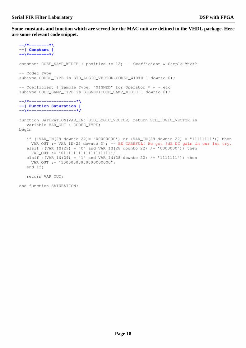
Some constants and function which are served for the MAC unit are defined in the VHDL package. Here are some relevant code snippet. --/*--------*\ --| Constant | --\*--------*/ constant COEF_SAMP_WIDTH : positive := 12; -- Coefficient & Sample Width -- Codec Type subtype CODEC_TYPE is STD_LOGIC_VECTOR(CODEC_WIDTH-1 downto 0); -- Coefficient & Sample Type, "SIGNED" for Operator * + - etc subtype COEF_SAMP_TYPE is SIGNED(COEF_SAMP_WIDTH-1 downto 0); --/*-------------------*\ --| Function Saturation | --\*-------------------*/ function SATURATION(VAR_IN: STD_LOGIC_VECTOR) return STD_LOGIC_VECTOR is variable VAR_OUT : CODEC_TYPE; begin if ((VAR_IN(29 downto 22)= "00000000") or (VAR_IN(29 downto 22) = "11111111")) then VAR_OUT := VAR_IN(22 downto 3); -- BE CAREFUL! We got 8dB DC gain in our 1st try. elsif ((VAR_IN(29) = '0' and VAR_IN(28 downto 22) /= "0000000")) then VAR_OUT := "01111111111111111111"; elsif ((VAR_IN(29) = '1' and VAR_IN(28 downto 22) /= "1111111")) then VAR_OUT := "10000000000000000000"; end if; return VAR_OUT; end function SATURATION;

Serial FIR Filter Laboratory DSP with FPGA
Page 19
Appendix 4. Source Code for Generating Telegramms in the Simulation library IEEE; use IEEE.STD_LOGIC_1164.all; entity TOP_FIR_TB is end entity TOP_FIR_TB; architecture TEST of TOP_FIR_TB is 긔긔 begin 긔긔 SDOUT_SIM : process begin -- In order to tune DLL module SDOUT_IP <= '0'; wait for 57200 ps; -->>> 1 Telegramm SDOUT_IP <= '0'; wait for 87900 ps; -- MSB <1> SDOUT_IP <= '1'; wait for 80*19 ns; -- <2-20> SDOUT_IP <= '0'; wait for 80 ns; -- <21> just for check SDOUT_IP <= '1'; wait for 80 ns; -- <22> just for check SDOUT_IP <= '0'; wait for 80*42 ns; -- <23-64> -- Each case should be activated alternatively, i.e., one case at -- one time -- case1: Step function, -- then we can see nearly "ONE" at output after 64 samples for i in 2 to 64 loop -->>> 2-64 Telegramms SDOUT_IP <= '0'; wait for 80 ns; -- MSB <1> SDOUT_IP <= '1'; wait for 80*19 ns; -- <2-20> SDOUT_IP <= '0'; wait for 80 ns; -- <21> just for check SDOUT_IP <= '1'; wait for 80 ns; -- <22> just for check SDOUT_IP <= '0'; wait for 80*42 ns; -- <23-64> end loop; -- case2: Impulse function, -- then we can detect each coefficient at output -- for i in 2 to 64 loop -- -- >>> 2-64 Telegramms -- SDOUT_IP <= '0'; wait for 80*64 ns; -- end loop; end process SDOUT_SIM; end architecture TEST;

Page 20
Figure: Zoom-out of functional simulation for impulse response
Output: each filter coefficient

Page 21
Figure: Zoom-in of functional simulation for impulse response
Serial FIR Filter Laboratory DSP with FPGA
Page 22
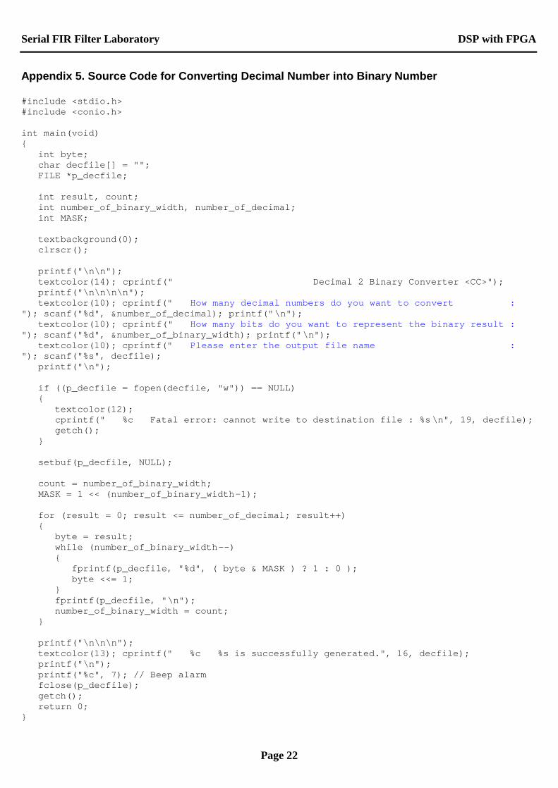
Appendix 5. Source Code for Converting Decimal Number into Binary Number #include <stdio.h> #include <conio.h> int main(void) { int byte; char decfile[] = ""; FILE *p_decfile; int result, count; int number_of_binary_width, number_of_decimal; int MASK; textbackground(0); clrscr(); printf("\n\n"); textcolor(14); cprintf(" Decimal 2 Binary Converter <CC>"); printf("\n\n\n\n"); textcolor(10); cprintf(" How many decimal numbers do you want to convert : "); scanf("%d", &number_of_decimal); printf("\n"); textcolor(10); cprintf(" How many bits do you want to represent the binary result : "); scanf("%d", &number_of_binary_width); printf("\n"); textcolor(10); cprintf(" Please enter the output file name : "); scanf("%s", decfile); printf("\n"); if ((p_decfile = fopen(decfile, "w")) == NULL) { textcolor(12); cprintf(" %c Fatal error: cannot write to destination file : %s\n", 19, decfile); getch(); } setbuf(p_decfile, NULL); count = number_of_binary_width; MASK = 1 << (number_of_binary_width-1); for (result = 0; result <= number_of_decimal; result++) { byte = result; while (number_of_binary_width--) { fprintf(p_decfile, "%d", ( byte & MASK ) ? 1 : 0 ); byte <<= 1; } fprintf(p_decfile, "\n"); number_of_binary_width = count; } printf("\n\n\n"); textcolor(13); cprintf(" %c %s is successfully generated.", 16, decfile); printf("\n"); printf("%c", 7); // Beep alarm fclose(p_decfile); getch(); return 0; }

Serial FIR Filter Laboratory DSP with FPGA
Page 23
This C program converts decimal number into x-bit binary number representation. For example, the user wants to convert number from 0 to 16 into 8-bit binary number representation. One example screen shot is shown as below for this case.
Here is the content of file ” result.txt„. 00000000 0 00000001 1 00000010 2 00000011 3 00000100 4 00000101 5 00000110 6 00000111 7 00001000 8 00001001 9 00001010 10 00001011 11 00001100 12 00001101 13 00001110 14 00001111 15 00010000 16

Serial FIR Filter Laboratory DSP with FPGA
Page 24
Appendix 6. VHDL Source Code Hierarchical Structure
ENTITY_FIR.vhd
TOP_FIR.vhd
CODEC_FPGA.vhd
FIR_PKG.vhd(package for the whole project)
MAC_FIR.vhd FSM_FIR.vhd
RAM_COEF_256_16.vhd RAM_SAMP_256_16.vhd
ADR_CNT_COEF.vhd ADR_CNT_SAMP.vhd
INTERFACE.vhd DLL_FIR.vhd
The FIR_PKG.vhd is the service package for the whole project, constants, Top Entity components and function are defined there. The top entity TOP_FIR.vhd combines the codec interface with FIR component together. The CODEC_FPGA.vhd contains the interface component and clock dll component. The ENTITY_FIR.vhd contains six sub-components: MAC unit, FSM controller, Coefficient RAM, Address counter for coefficient RAM, Sample RAM, Address counter for sample RAM. For each vhd file a corresponding testbench file is developped. It“s named with _TB suffix. All source code can be found in the attached floppy disk. The file structures are defined as follows: -> Auxililary includes C Tool dec2bin.exe, FIR coefficient list, Matlab source file -> Report includes the electronic version of this report (PDF format), the timing diagram etc are also included in order for the user to have access to the result, for his/her convienience. The prerequisite is that the user should install Microsoft Visio 2000 on the local machine. -> Src includes all VHDL package and source files -> Testbench includes all VHDL testbenches -> UCF includes the User Constraint File (UCF) files for Xilinx ISE 4.x implementation

Page 25
Here we want to express our thanks to Prof. Dr. Schwarz for providing us an interesting elective course for our master study and patient guiding during each laboratory date. We strongly recommend our new ”Information Engineering晦 master course students to take part in the selective course - ”DSP with FPGAs晦 with Prof. Dr. Schwarz! Signature ____________________ ____________________ ____________________
Hamburg, 16. July 2003