Lab on a Chip - bioeeweb.ee.columbia.edu · Electrowetting-on-dielectric microfluidics are actively...
9
Lab on a Chip PAPER Cite this: DOI: 10.1039/c4lc00443d Received 14th April 2014, Accepted 15th August 2014 DOI: 10.1039/c4lc00443d www.rsc.org/loc An integrated CMOS quantitative-polymerase- chain-reaction lab-on-chip for point-of-care diagnostics† Haig Norian, Ryan M. Field, Ioannis Kymissis and Kenneth L. Shepard * Considerable effort has recently been directed toward the miniaturization of quantitative-polymerase- chain-reaction (qPCR) instrumentation in an effort to reduce both cost and form factor for point-of-care applications. Considerable gains have been made in shrinking the required volumes of PCR reagents, but resultant prototypes retain their bench-top form factor either due to heavy heating plates or cumbersome optical sensing instrumentation. In this paper, we describe the use of complementary-metal-oxide semiconductor (CMOS) integrated circuit (IC) technology to produce a fully integrated qPCR lab-on-chip. Exploiting a 0.35 μm high-voltage CMOS process, the IC contains all of the key components for performing qPCR. Integrated resistive heaters and temperature sensors regulate the surface temperature of the chip to an accuracy of 0.45 °C. Electrowetting-on-dielectric microfluidics are actively driven from the chip surface, allowing for droplet generation and transport down to volumes less than 1.2 nanoliter. Integrated single-photon avalanche diodes (SPADs) are used for fluorescent monitoring of the reaction, allowing for the quantification of target DNA with more than four-orders-of-magnitude of dynamic range and sensitivities down to a single copy per droplet. Using this device, reliable and sensitive real-time proof-of-concept detection of Staphylococcus aureus (S. aureus) is demonstrated. Introduction Quantitative polymerase chain reaction (qPCR) has become one of the most widely used methods for the quantification and detection of both DNA and messenger RNA (after reverse transcription) due to its accuracy, sensitivity and large dynamic range. 1 As an example, infectious disease recognition through qPCR relies upon the selective amplification and subsequent detection of a DNA sequence that has been shown to be unique to a particular pathogen. The concentration of DNA present in a test volume after each iteration of a tem- perature cycling protocol is monitored in real time. As a result, the initial copy number of the target can be determined given the controlled, known amplification at each step. Commercial qPCR systems, which generally operate on standard volumes of 25 or 50 μL, require a heating block weighing anywhere from 2 to 10 kg to ensure a uniform temperature profile across a multiwell plate, leading to (at best) a bench-top form factor. While previous work has brought the volume of a single qPCR reaction down to volumes as low as 10 pL, easing some of the temperature uniformity requirements, 2–6 these systems have either relied on external optics for fluorescence detection or lacked inte- grated droplet formation. 3,4,7–10 In the first case, the sensing of fluorescent dyes requires bulky and delicate optics to obtain a reliable measurement, and in the second case, any integrated microfluidics have to rely on pneumatic control, regulated by external pumps. Overall form factor remains that of a stationary, bench-top device. Complementary metal-oxide-semiconductor (CMOS) inte- grated circuit (IC) technology provides a unique opportu- nity to further scale PCR hardware by providing for high- bandwidth, distributed temperature control across the chip surfaces and integrated detection. Toumazou et al. 11 describe the first CMOS-based qPCR IC. Instead of using fluorescence detection, pH is monitored during PCR to gauge the progres- sion of the reaction with heating and temperature control also performed on-chip. 11 This device is still limited by use of microfluidic pumps, requiring reagent volume on the microliter scale. Sensitivity is limited by noise in the inte- grated ion-sensitive field-effect transistors to 10 copies per sample. Electrowetting-on-dielectric (EWoD) droplet transport provides a means for scaling microfluidics by controlling droplets electrically without the need for external pumps. In the presence of an electric field, a droplet of aqueous reagent seeks to minimize its internal energy through translational Lab Chip This journal is © The Royal Society of Chemistry 2014 Columbia University, Department of Electrical Engineering, 500 W. 120th St., New York, New York 10027, USA. E-mail: [email protected] † Electronic supplementary information (ESI) available. See DOI: 10.1039/ c4lc00443d Published on 15 August 2014. Downloaded by Columbia University on 05/09/2014 20:31:11. View Article Online View Journal
Transcript of Lab on a Chip - bioeeweb.ee.columbia.edu · Electrowetting-on-dielectric microfluidics are actively...

Lab on a Chip
Publ
ishe
d on
15
Aug
ust 2
014.
Dow
nloa
ded
by C
olum
bia
Uni
vers
ity o
n 05
/09/
2014
20:
31:1
1.
PAPER View Article OnlineView Journal
This journal is © The Royal Society of Chemistry 2014
Columbia University, Department of Electrical Engineering, 500 W. 120th St.,
New York, New York 10027, USA. E-mail: [email protected]
† Electronic supplementary information (ESI) available. See DOI: 10.1039/c4lc00443d
Cite this: DOI: 10.1039/c4lc00443d
Received 14th April 2014,Accepted 15th August 2014
DOI: 10.1039/c4lc00443d
www.rsc.org/loc
An integrated CMOS quantitative-polymerase-chain-reaction lab-on-chip for point-of-carediagnostics†
Haig Norian, Ryan M. Field, Ioannis Kymissis and Kenneth L. Shepard*
Considerable effort has recently been directed toward the miniaturization of quantitative-polymerase-
chain-reaction (qPCR) instrumentation in an effort to reduce both cost and form factor for point-of-care
applications. Considerable gains have been made in shrinking the required volumes of PCR reagents, but
resultant prototypes retain their bench-top form factor either due to heavy heating plates or cumbersome
optical sensing instrumentation. In this paper, we describe the use of complementary-metal-oxide
semiconductor (CMOS) integrated circuit (IC) technology to produce a fully integrated qPCR lab-on-chip.
Exploiting a 0.35 μm high-voltage CMOS process, the IC contains all of the key components for
performing qPCR. Integrated resistive heaters and temperature sensors regulate the surface temperature of
the chip to an accuracy of 0.45 °C. Electrowetting-on-dielectric microfluidics are actively driven from the
chip surface, allowing for droplet generation and transport down to volumes less than 1.2 nanoliter.
Integrated single-photon avalanche diodes (SPADs) are used for fluorescent monitoring of the reaction,
allowing for the quantification of target DNA with more than four-orders-of-magnitude of dynamic range
and sensitivities down to a single copy per droplet. Using this device, reliable and sensitive real-time
proof-of-concept detection of Staphylococcus aureus (S. aureus) is demonstrated.
Introduction
Quantitative polymerase chain reaction (qPCR) has becomeone of the most widely used methods for the quantificationand detection of both DNA and messenger RNA (after reversetranscription) due to its accuracy, sensitivity and largedynamic range.1 As an example, infectious disease recognitionthrough qPCR relies upon the selective amplification andsubsequent detection of a DNA sequence that has been shownto be unique to a particular pathogen. The concentration ofDNA present in a test volume after each iteration of a tem-perature cycling protocol is monitored in real time. As a result,the initial copy number of the target can be determined giventhe controlled, known amplification at each step.
Commercial qPCR systems, which generally operate onstandard volumes of 25 or 50 μL, require a heating blockweighing anywhere from 2 to 10 kg to ensure a uniformtemperature profile across a multiwell plate, leading to (atbest) a bench-top form factor. While previous work hasbrought the volume of a single qPCR reaction down tovolumes as low as 10 pL, easing some of the temperature
uniformity requirements,2–6 these systems have either reliedon external optics for fluorescence detection or lacked inte-grated droplet formation.3,4,7–10 In the first case, the sensingof fluorescent dyes requires bulky and delicate optics toobtain a reliable measurement, and in the second case, anyintegrated microfluidics have to rely on pneumatic control,regulated by external pumps. Overall form factor remainsthat of a stationary, bench-top device.
Complementary metal-oxide-semiconductor (CMOS) inte-grated circuit (IC) technology provides a unique opportu-nity to further scale PCR hardware by providing for high-bandwidth, distributed temperature control across the chipsurfaces and integrated detection. Toumazou et al.11 describethe first CMOS-based qPCR IC. Instead of using fluorescencedetection, pH is monitored during PCR to gauge the progres-sion of the reaction with heating and temperature controlalso performed on-chip.11 This device is still limited by useof microfluidic pumps, requiring reagent volume on themicroliter scale. Sensitivity is limited by noise in the inte-grated ion-sensitive field-effect transistors to 10 copies persample.
Electrowetting-on-dielectric (EWoD) droplet transportprovides a means for scaling microfluidics by controllingdroplets electrically without the need for external pumps. Inthe presence of an electric field, a droplet of aqueous reagentseeks to minimize its internal energy through translational
Lab Chip
Lab on a ChipPaper
Publ
ishe
d on
15
Aug
ust 2
014.
Dow
nloa
ded
by C
olum
bia
Uni
vers
ity o
n 05
/09/
2014
20:
31:1
1.
View Article Online
motion toward the direction of positive voltage.12–15 Nearlyall EWoD devices are passive; that is, they have no integratedmeans to control or generate controlling voltages.15–17 EWoDdevices employed for qPCR applications have been limited tosuch passive devices with external fluorescence detection.18,19
The one active CMOS EWoD device that has been reportedwas applied to the movement of cells through microfluidicchamber at speeds up to 30 μm s20 – with off-chip detection.The required voltage for EWoD transport (70–250 V, dependingon the size of the droplet) is also generated off-chip inthis design.
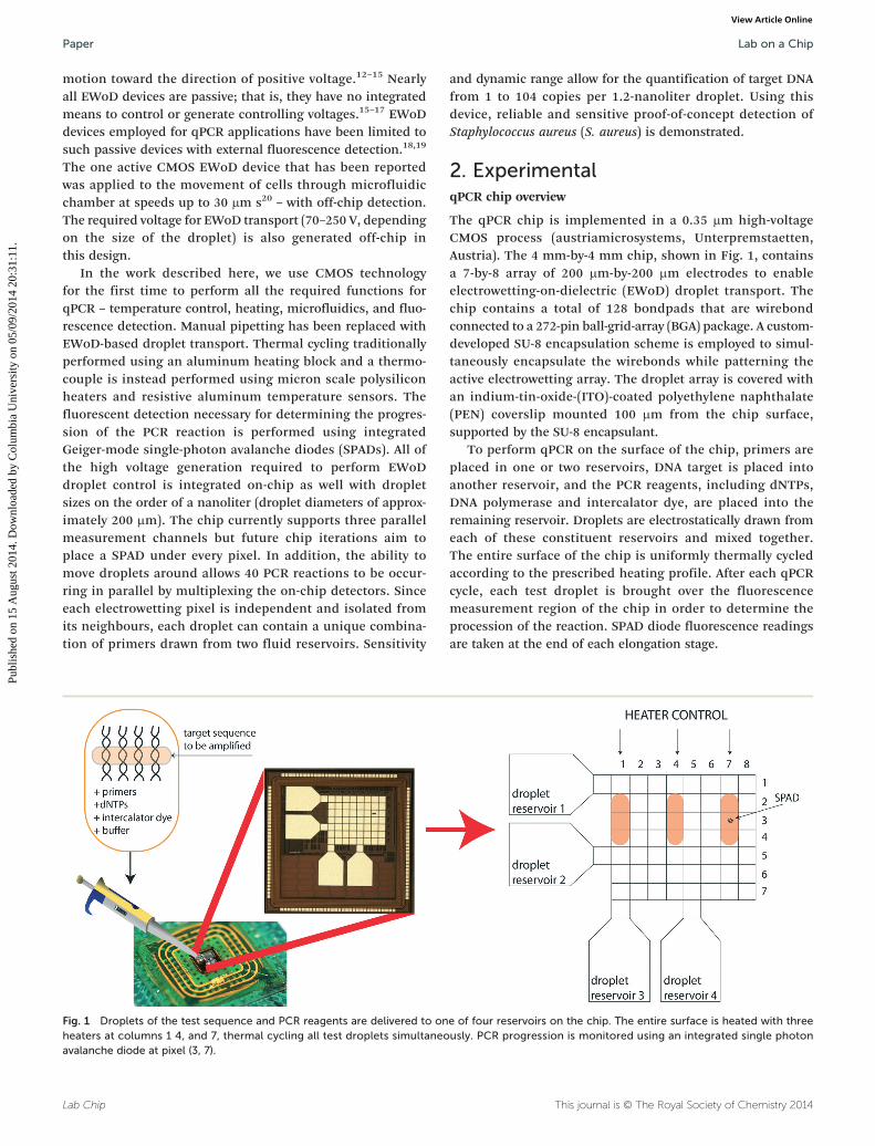
In the work described here, we use CMOS technologyfor the first time to perform all the required functions forqPCR – temperature control, heating, microfluidics, and fluo-rescence detection. Manual pipetting has been replaced withEWoD-based droplet transport. Thermal cycling traditionallyperformed using an aluminum heating block and a thermo-couple is instead performed using micron scale polysiliconheaters and resistive aluminum temperature sensors. Thefluorescent detection necessary for determining the progres-sion of the PCR reaction is performed using integratedGeiger-mode single-photon avalanche diodes (SPADs). All ofthe high voltage generation required to perform EWoDdroplet control is integrated on-chip as well with dropletsizes on the order of a nanoliter (droplet diameters of approx-imately 200 μm). The chip currently supports three parallelmeasurement channels but future chip iterations aim toplace a SPAD under every pixel. In addition, the ability tomove droplets around allows 40 PCR reactions to be occur-ring in parallel by multiplexing the on-chip detectors. Sinceeach electrowetting pixel is independent and isolated fromits neighbours, each droplet can contain a unique combina-tion of primers drawn from two fluid reservoirs. Sensitivity
Lab Chip
Fig. 1 Droplets of the test sequence and PCR reagents are delivered to onheaters at columns 1 4, and 7, thermal cycling all test droplets simultaneoavalanche diode at pixel (3, 7).
and dynamic range allow for the quantification of target DNAfrom 1 to 104 copies per 1.2-nanoliter droplet. Using thisdevice, reliable and sensitive proof-of-concept detection ofStaphylococcus aureus (S. aureus) is demonstrated.
2. ExperimentalqPCR chip overview
The qPCR chip is implemented in a 0.35 μm high-voltageCMOS process (austriamicrosystems, Unterpremstaetten,Austria). The 4 mm-by-4 mm chip, shown in Fig. 1, containsa 7-by-8 array of 200 μm-by-200 μm electrodes to enableelectrowetting-on-dielectric (EWoD) droplet transport. Thechip contains a total of 128 bondpads that are wirebondconnected to a 272-pin ball-grid-array (BGA) package. A custom-developed SU-8 encapsulation scheme is employed to simul-taneously encapsulate the wirebonds while patterning theactive electrowetting array. The droplet array is covered withan indium-tin-oxide-(ITO)-coated polyethylene naphthalate(PEN) coverslip mounted 100 μm from the chip surface,supported by the SU-8 encapsulant.
To perform qPCR on the surface of the chip, primers areplaced in one or two reservoirs, DNA target is placed intoanother reservoir, and the PCR reagents, including dNTPs,DNA polymerase and intercalator dye, are placed into theremaining reservoir. Droplets are electrostatically drawn fromeach of these constituent reservoirs and mixed together.The entire surface of the chip is uniformly thermally cycledaccording to the prescribed heating profile. After each qPCRcycle, each test droplet is brought over the fluorescencemeasurement region of the chip in order to determine theprocession of the reaction. SPAD diode fluorescence readingsare taken at the end of each elongation stage.
This journal is © The Royal Society of Chemistry 2014
e of four reservoirs on the chip. The entire surface is heated with threeusly. PCR progression is monitored using an integrated single photon

Lab on a Chip Paper
Publ
ishe
d on
15
Aug
ust 2
014.
Dow
nloa
ded
by C
olum
bia
Uni
vers
ity o
n 05
/09/
2014
20:
31:1
1.
View Article Online
Electrowetting droplet transport
The pixel dimension of 200 μm allows for a droplet size ofapproximately 1.2 nanoliter to be supported. The EWoD con-trol circuitry is shown in Fig. 2. Each electrode is controlledto have a voltage of either VDD-HV = 90 V or 0 V relative to thevoltage on the ITO-coated PEN coverslip. In each pixel, a con-trol bit is latched to indicate this state, and this latched valueis level-shifted from the 3.3 V core voltage level to VDD-HV atthe electrode. The pixel control bits are loaded in parallelfrom eight data lines on a row basis (determined form adecoded three-bit row address). The bits associated with Row8 determine the potential for the four reservoirs and theelectrodes connecting these to the 7-by-8 array (see Fig. 1). Arow can be updated every 10 msec.
An on-chip charge pump steps up the 3.3 V core logicsupply voltage to generate the 90 V VDD-HV supply. Typically,each stage of a typical Dickson charge pump configurationconsists of a diode-connected transistor and a capacitor.21 Toimprove efficiency, a three-transistor-based stage is used inour implementation (see Fig. 2). Transistors M1, M2, M3
are high voltage devices capable of supporting drain-bodyand drain-source voltages of up to 120 V. MC2 turns on whenthe diode-connected transistor MC3 is off, establishing zerobias across the drain-body diode of MC3. By preventing theflow of current across this diode junction during operation,
This journal is © The Royal Society of Chemistry 2014
Fig. 2 The electrowetting control circuitry allows the state of an eight-pix3.3 V logic with the 90 V electrowetting voltage generated either from the o
efficiency is increased. Transistor MC1 turns on when MC3 ison, eliminating body-effect enhancement of the thresholdvoltage of MC3, reducing the drain-to-source voltage dropacross this device.
The level shifter in each pixel makes use of high voltagetransistors ML1, ML2, ML3, MR1, MR2, and MR3 that can toleratedrain-bulk voltages of 120 V, allowing for the safe use of aVDD-HV of 90 V. Furthermore, the use of cascode transistorsML2 and MR2 prevents the gate voltages of ML3 and MR3 fromexceeding 25 V.
SPADs in CMOS
The CMOS-integrated SPAD design here follows one previousused for a SPAD-based imager.22 This SPAD is located untilpixel (7, 3) in Fig. 1. An area of 100 μm2 is removed from theelectrode area for this pixel to form a window for light topass with no noticeable effects on EWoD transport. TheSPAD's shallow p+ region has a diameter of 7.5 μm in ann-well of diameter 15 μm, as shown in the inset of Fig. 3.
The diode is biased beyond its reverse breakdown voltage(approximately Vbreakdown = 20 V) by an overvoltage, Vov. Withcareful engineering of the implants to avoid deep-level traps,the device does not draw any current until a photon triggersan avalanche. Geiger mode of operation of the SPAD requiresa circuit which reduces the reverse bias across the diode to
Lab Chip
el row to be updated every 10 ms. A custom level shifter interfaces then-chip Dickson charge pump.
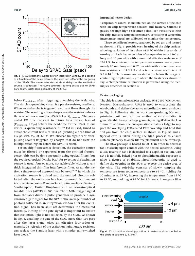
Fig. 3 SPAD avalanche events over an integration window of 1 secondas a function of the delay between the laser turn-off and the on-gatingof the SPAD. The curve saturates at short delays as the excitationsource is collected. The curve saturates at long delays due to SPADdark count. Inset: basic geometry of the SPAD.
Fig. 4 Cross section showing position of heaters and sensors belowthe pixels in columns 1, 4, and 7.
Lab on a ChipPaper
Publ
ishe
d on
15
Aug
ust 2
014.
Dow
nloa
ded
by C
olum
bia
Uni
vers
ity o
n 05
/09/
2014
20:
31:1
1.
View Article Online
below Vbreakdown after triggering, quenching the avalanche.The simplest quenching circuit is a passive resistor, used here.When an avalanche is triggered, a current flows through theresistor. The resulting voltage drop across the resistor reducesthe reverse bias across the SPAD below Vbreakdown. The asso-ciated RC time constant to return to a reverse bias of(Vbreakdown + VOV) defines the dead-time for the SPAD. In ourdevice, a quenching resistance of 67 kΩ is used, tuned toavalanche current levels of 10.3 μA, yielding a dead-time of0.5 μs with Vov of 3.5 V. We observe no significant after-pulsing (events triggered by charges that do not clear themultiplication region before the SPAD is reset).
For on-chip fluorescence detection, the excitation sourcemust be filtered or separated from the emitted fluores-cence. This can be done spectrally using optical filters, butthe required optical density (OD) for rejecting the excitationsource is usual four or more, not achievable without a verythick integrated thin-film interference filter. As an alterna-tive, a time-resolved approach can be used23,24 in which theexcitation source is pulsed and the emitted photons col-lected after the excitation has been removed. Our currentinstrumentation uses a Fianium Supercontinuum laser (Fianium,Southampton, United Kingdom) with an acousto-opticaltunable filter (AOTF) at 500 nm. The 1 MHz trigger signalfrom the laser drives a pulse generator to produce a syn-chronized gate signal for the SPAD. The average number ofphotons collected in an integration window after the excita-tion signal has been shut off determines the measuredintensity. Timing of the gate signal is important to ensurethat excitation light is not collected by the SPAD. As shownin Fig. 3, enabling the gate of the SPAD more than 100 psecafter the laser signal gives an effective four-orders-of-magnitude rejection of the excitation light. Future revisionscan replace the Fianium laser with a simpler gain-switchedlaser diode.25
Lab Chip
Integrated heater design
Temperature control is maintained on the surface of the chipwith on-chip temperature sensors and heaters. Current ispassed through high-resistance polysilicon resistors to heatthe chip. Resistive temperature sensors consisting of serpentineinterconnect metal are calibrated to monitor the temperature.
Three polysilicon heaters, separated by 400 μm and locatedas shown in Fig. 1, provide even heating of the chip surface,allowing variation of less than ±1.5 °C within 3 seconds ofturning on. Each heater consists of a serpentine trace 5300 μmlong and 20 μm wide with a nominal effective resistance of270 kΩ. In contrast, the temperature sensors are approxi-mately 80 mm long and 0.67 μm wide with a room tempera-ture resistance of 4.3 kΩ and a temperature coefficient of3.3 × 10−3. The sensors are located 4 μm below the reagent-containing droplet and 6 μm above the heaters as shown inFig. 4. Temperature calibration is performed using the tech-niques described in section 3.
Device packaging
The chip is mounted on a BGA package. SU-8 2100 (Microchem,Newton, Massachusetts, USA) is used to encapsulate thewirebonds and define the active microfluidic area, as shownin Fig. 6. Following similar work encapsulating ICs ontoprinted-circuit boards,26 our method of encapsulation isgeneralizable to any package geometry using SU-8 as thick as1 mm. In addition, the encapsulation creates a ledge to sup-port the overlaying ITO-coated PEN coverslip and hold this100 μm from the chip surface as shown in Fig. 5a and c.Special care is taken during the SU-8 process to ensuresuitable planarity to allow tilt-free placement of the coverslip.
The BGA package is heated to 70 °C in order to decreaseSU-8 viscosity upon contact with the heated substrate. Usinga PEN reservoir, SU-8 is deposited to a depth of 800 μm. CastSU-8 is not fully baked prior to photolithographic exposure toallow a degree of pliability. Photolithography is used todefine the opening in the SU-8 to expose the active area ofthe chip. The soft-bake consists of slowly ramping thetemperature from room temperature to 65 °C, holding for30 minutes at 65 °C, increasing the temperature from 65 °Cto 95 °C, and holding at 95 °C for 8.5 hours. A longpass filter
This journal is © The Royal Society of Chemistry 2014

Fig. 5 (a) Fully encapsulated PCR chip using SU8 to protect thewirebonds. (b) Sidewalls have gradient of 89.9° enabled with use oflong-pass filter during UV exposure. (c) A special coverslip is used tocompress the droplet and improve electrowetting droplet transport.
Fig. 6 qPCR thermal cycling profile. Temperature reading taken fromcenter sensor.
Lab on a Chip Paper
Publ
ishe
d on
15
Aug
ust 2
014.
Dow
nloa
ded
by C
olum
bia
Uni
vers
ity o
n 05
/09/
2014
20:
31:1
1.
View Article Online
with a cutoff wavelength of 360 nm is used for exposure,resulting in sidewall gradients of 89.9°, as shown in Fig. 5b.
Following the SU-8 patterning, a conformal coating of2 μm of Parlyene C is deposited on the chip surface to pro-vide adequate dielectric isolation of the EWoD electrodes.Deposition is performed using the Labcoater2 Parylene Depo-sition Chamber (Specialty Coating Services, Indianapolis,Indiana). To increase the hydrophobicity of the dielectriclayer, a 100 nm-thick layer of Teflon AF (DuPont, New York,New York) is spin coated on top of the Parylene-C. This dielec-tric surface is noted in the inset to Fig. 5c. The detailed pro-cess flow on the post-processing steps performed on thechip is given in the ESI.† Following this post-processing,the electrowetting areas of the chip are planar to 0.2 μm.
This journal is © The Royal Society of Chemistry 2014
3. ResultsIntegrated temperature sensor calibration using a‘DNA thermometer’
The embedded heaters, calibrated with DNA melting, areused along with the temperature sensors and proportional–integral–differential (PID) control to produce the requisiteqPCR heating profiles. All three heaters are run together withtemperature measurement taken from the center sensor forcontrol. Readings from the center resistive temperature sen-sor are shown in Fig. 6 during representative thermal cycling.With the use of a PID control loop, the surface heats from72 °C to 94 °C in 11 s, from 94 °C to 60 °C in 13 seconds,and from 60 °C to 72 °C in 8 seconds. The maximum rippleobserved is 0.45 °C. No active cooling is required; cooling atof up to −3 °C per second occurs by means of heat sinkingthrough the very thermally conducting silicon substrate.
In order to calibrate the temperature sensors to the drop-let temperature on the chip surface, we developed a methodusing DNA contained in the droplet as an active temperaturesensing material. Our approach builds on previous work27,28
and uses DNA melting, as tracked by an intercalator dye, todetermine temperature. A single 12-base oligonucleotide canachieve a dynamic range of approximately 10 °C. DINAMELTis used in the sequence design to simulate oligonucleotidemelting and obtain the required melting temperature andprofile.29 Special care is taken to avoid strands that exhibitself-folding tendencies. Many factors influence the meltingtemperature and slope. Longer sequences (>50 bp) with arandom assortment of nucleotides will typically have very highmelting temperatures approaching 94 °C. Shorter sequenceswill have lower melting temperatures with a slope highlydependent on the sequence. Sequences with high concentra-tion of guanine–cytosine pairs will have broad melting curvesdue to strength of the inter-base bonds, but too many G–Cpairs should be avoided to prevent excessive single-strandfolding. For the calibration here, we use the sequenceAAAGGAAAGGAAAAGGAAAAGG with a melting temperatureof 72 °C and calibration curve shown in Fig. 7a.
Lab Chip
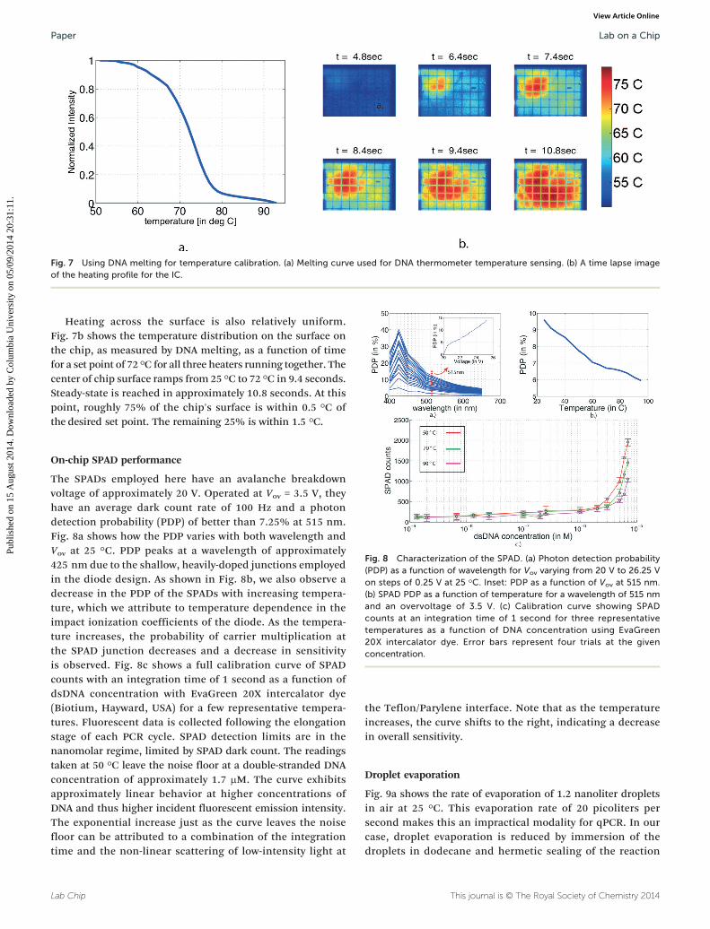
Fig. 7 Using DNA melting for temperature calibration. (a) Melting curve used for DNA thermometer temperature sensing. (b) A time lapse imageof the heating profile for the IC.
Lab on a ChipPaper
Publ
ishe
d on
15
Aug
ust 2
014.
Dow
nloa
ded
by C
olum
bia
Uni
vers
ity o
n 05
/09/
2014
20:
31:1
1.
View Article Online
Heating across the surface is also relatively uniform.Fig. 7b shows the temperature distribution on the surface onthe chip, as measured by DNA melting, as a function of timefor a set point of 72 °C for all three heaters running together. Thecenter of chip surface ramps from 25 °C to 72 °C in 9.4 seconds.Steady-state is reached in approximately 10.8 seconds. At thispoint, roughly 75% of the chip's surface is within 0.5 °C ofthe desired set point. The remaining 25% is within 1.5 °C.
Fig. 8 Characterization of the SPAD. (a) Photon detection probability(PDP) as a function of wavelength for Vov varying from 20 V to 26.25 Von steps of 0.25 V at 25 °C. Inset: PDP as a function of Vov at 515 nm.(b) SPAD PDP as a function of temperature for a wavelength of 515 nmand an overvoltage of 3.5 V. (c) Calibration curve showing SPADcounts at an integration time of 1 second for three representativetemperatures as a function of DNA concentration using EvaGreen20X intercalator dye. Error bars represent four trials at the givenconcentration.
On-chip SPAD performance
The SPADs employed here have an avalanche breakdownvoltage of approximately 20 V. Operated at Vov = 3.5 V, theyhave an average dark count rate of 100 Hz and a photondetection probability (PDP) of better than 7.25% at 515 nm.Fig. 8a shows how the PDP varies with both wavelength andVov at 25 °C. PDP peaks at a wavelength of approximately425 nm due to the shallow, heavily-doped junctions employedin the diode design. As shown in Fig. 8b, we also observe adecrease in the PDP of the SPADs with increasing tempera-ture, which we attribute to temperature dependence in theimpact ionization coefficients of the diode. As the tempera-ture increases, the probability of carrier multiplication atthe SPAD junction decreases and a decrease in sensitivityis observed. Fig. 8c shows a full calibration curve of SPADcounts with an integration time of 1 second as a function ofdsDNA concentration with EvaGreen 20X intercalator dye(Biotium, Hayward, USA) for a few representative tempera-tures. Fluorescent data is collected following the elongationstage of each PCR cycle. SPAD detection limits are in thenanomolar regime, limited by SPAD dark count. The readingstaken at 50 °C leave the noise floor at a double-stranded DNAconcentration of approximately 1.7 μM. The curve exhibitsapproximately linear behavior at higher concentrations ofDNA and thus higher incident fluorescent emission intensity.The exponential increase just as the curve leaves the noisefloor can be attributed to a combination of the integrationtime and the non-linear scattering of low-intensity light at
Lab Chip
the Teflon/Parylene interface. Note that as the temperatureincreases, the curve shifts to the right, indicating a decreasein overall sensitivity.
Droplet evaporation
Fig. 9a shows the rate of evaporation of 1.2 nanoliter dropletsin air at 25 °C. This evaporation rate of 20 picoliters persecond makes this an impractical modality for qPCR. In ourcase, droplet evaporation is reduced by immersion of thedroplets in dodecane and hermetic sealing of the reaction
This journal is © The Royal Society of Chemistry 2014

Fig. 9 a.) Droplet evaporation in air at 25 °C. b.) Droplet evaporationin dodecane with and with the use of a coverslip during a complete30-cycle PCR thermal cycling run.
Fig. 10 Longterm electrowetting droplet transport testing. Increase inthreshold voltage is due to decrease in surface hydrophobicity due tosurface charge collection.
Lab on a Chip Paper
Publ
ishe
d on
15
Aug
ust 2
014.
Dow
nloa
ded
by C
olum
bia
Uni
vers
ity o
n 05
/09/
2014
20:
31:1
1.
View Article Online
cavity on the chip. Fig. 9b illustrates the decrease in dropletvolume as typical PCR thermal cycling (Fig. 6) is performedon a 1.2 nanoliter droplet in dodecane with and without acoverslip. Without the coverslip, evaporation still occurs atan unacceptably high rate of 1.9 picoliter per second (Fig. 9b).By hermetically sealing the reaction cavity with the PENcoverslip, this evaporation rate is reduced to 6.3 femtoliterper second (Fig. 9b), resulting in a volume reduction ofless than 1% during the 3600 s that characterize a typicalqPCR run.
Performance of electrowettting droplet transport
The non-specific binding of biomolecules to the surface ofParylene-C/Teflon-AF dielectric has been shown to degradethe surface's hydrophobicity.30 This factor was evaluatedon our test chip using droplets containing the S. aureusPCR mixture. The threshold voltage necessary for dropletactuation is plotted as a function of number of actuationsin Fig. 10. This test consisted of a ~1.2 nL droplet beingtransported between set of adjacent electrowetting pixels.ESI† Video S1 shows a representative droplet movement forthis test. Note that a significant increase in the necessary
This journal is © The Royal Society of Chemistry 2014
electrowetting actuation voltage does not occur until afterapproximately 200 actuations, allowing significant use of thechip before this becomes a factor.
The hydrophobic interaction between water, dodecane,and electrowetting surface is expected to show a temperaturedependence.31 Using the same actuation test in which a 1.2 nLdroplet is transported between two adjacent electrowettingpixels, the threshold voltage necessary for droplet actua-tion is plotted as a function of temperature in Fig. 12.Note that a significant increase in the electrowettingthreshold voltage for our particular configuration does notoccur until temperatures over 110 °C. The available 90 Vactuation voltage satisfies the necessary temperature rangefor this device.
Performance of real time PCR
As a proof-of-concept for our device, we amplify and detect a364-base sequence characteristic for S. aureus (Norgen BiotekCorporation, Thorold, Canada). Fig. 11 shows qPCR datafrom individual droplets with serial dilutions of the targetstrand from 1000 down to 1 copy per droplet.
Each test droplet comes from mixing PCR reagents, inter-calator dye, DNA target, and buffer (Fig. 13). While we havesuccessfully actuated 1.2 nL droplets, we get more consistentresults from 3 nL droplets, which occupy approximately fourpixels in the electrowetting array. Larger droplets impingemore of the higher fringing fields found at the edges of thesquare electrodes, allowing for easier movement. A videoshowing droplet transport for 3 nL droplets on the surface ofthe chip is given in ESI† Video S2.
The reagent consumption per qPCR test is reducedmore than 40 000-fold compared to a conventional qPCRassay. For the full range of initial concentrations from1 to 10 000 copies per droplet, we obtain the expected linearrelationship between cycle threshold and the logarithm ofinitial concentration (Fig. 14) with a standard deviation of
Lab Chip
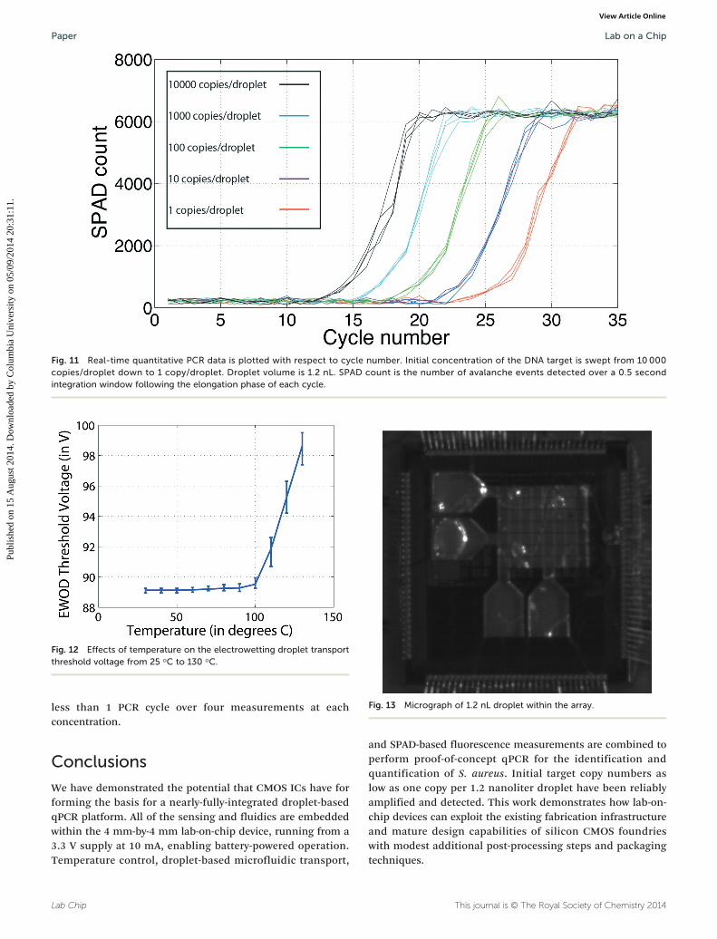
Fig. 11 Real-time quantitative PCR data is plotted with respect to cycle number. Initial concentration of the DNA target is swept from 10000copies/droplet down to 1 copy/droplet. Droplet volume is 1.2 nL. SPAD count is the number of avalanche events detected over a 0.5 secondintegration window following the elongation phase of each cycle.
Fig. 13 Micrograph of 1.2 nL droplet within the array.
Fig. 12 Effects of temperature on the electrowetting droplet transportthreshold voltage from 25 °C to 130 °C.
Lab on a ChipPaper
Publ
ishe
d on
15
Aug
ust 2
014.
Dow
nloa
ded
by C
olum
bia
Uni
vers
ity o
n 05
/09/
2014
20:
31:1
1.
View Article Online
less than 1 PCR cycle over four measurements at eachconcentration.
Conclusions
We have demonstrated the potential that CMOS ICs have forforming the basis for a nearly-fully-integrated droplet-basedqPCR platform. All of the sensing and fluidics are embeddedwithin the 4 mm-by-4 mm lab-on-chip device, running from a3.3 V supply at 10 mA, enabling battery-powered operation.Temperature control, droplet-based microfluidic transport,
Lab Chip
and SPAD-based fluorescence measurements are combined toperform proof-of-concept qPCR for the identification andquantification of S. aureus. Initial target copy numbers aslow as one copy per 1.2 nanoliter droplet have been reliablyamplified and detected. This work demonstrates how lab-on-chip devices can exploit the existing fabrication infrastructureand mature design capabilities of silicon CMOS foundrieswith modest additional post-processing steps and packagingtechniques.
This journal is © The Royal Society of Chemistry 2014
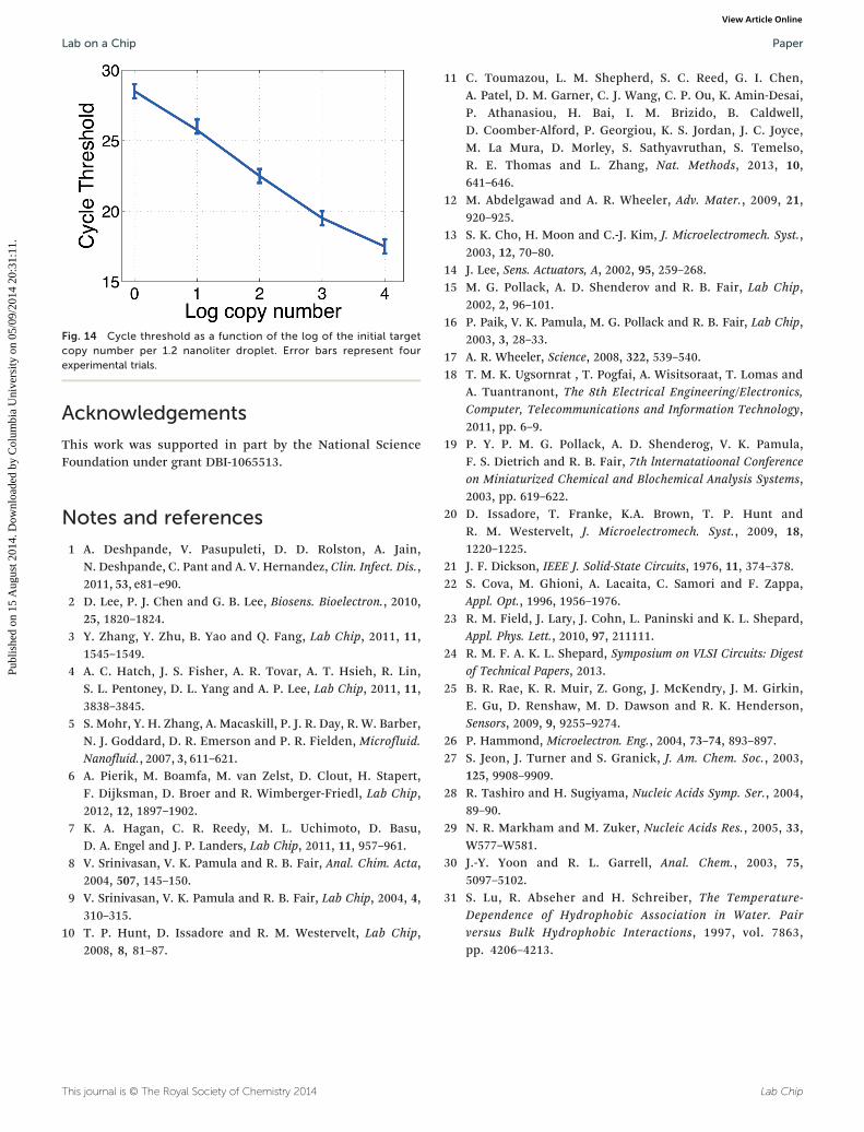
Fig. 14 Cycle threshold as a function of the log of the initial targetcopy number per 1.2 nanoliter droplet. Error bars represent fourexperimental trials.
Lab on a Chip Paper
Publ
ishe
d on
15
Aug
ust 2
014.
Dow
nloa
ded
by C
olum
bia
Uni
vers
ity o
n 05
/09/
2014
20:
31:1
1.
View Article Online
Acknowledgements
This work was supported in part by the National ScienceFoundation under grant DBI-1065513.
Notes and references
1 A. Deshpande, V. Pasupuleti, D. D. Rolston, A. Jain,
N. Deshpande, C. Pant and A. V. Hernandez, Clin. Infect. Dis.,2011, 53, e81–e90.2 D. Lee, P. J. Chen and G. B. Lee, Biosens. Bioelectron., 2010,
25, 1820–1824.3 Y. Zhang, Y. Zhu, B. Yao and Q. Fang, Lab Chip, 2011, 11,
1545–1549.4 A. C. Hatch, J. S. Fisher, A. R. Tovar, A. T. Hsieh, R. Lin,
S. L. Pentoney, D. L. Yang and A. P. Lee, Lab Chip, 2011, 11,3838–3845.5 S. Mohr, Y. H. Zhang, A. Macaskill, P. J. R. Day, R. W. Barber,
N. J. Goddard, D. R. Emerson and P. R. Fielden, Microfluid.Nanofluid., 2007, 3, 611–621.6 A. Pierik, M. Boamfa, M. van Zelst, D. Clout, H. Stapert,
F. Dijksman, D. Broer and R. Wimberger-Friedl, Lab Chip,2012, 12, 1897–1902.7 K. A. Hagan, C. R. Reedy, M. L. Uchimoto, D. Basu,
D. A. Engel and J. P. Landers, Lab Chip, 2011, 11, 957–961.8 V. Srinivasan, V. K. Pamula and R. B. Fair, Anal. Chim. Acta,
2004, 507, 145–150.9 V. Srinivasan, V. K. Pamula and R. B. Fair, Lab Chip, 2004, 4,
310–315.10 T. P. Hunt, D. Issadore and R. M. Westervelt, Lab Chip,
2008, 8, 81–87.This journal is © The Royal Society of Chemistry 2014
11 C. Toumazou, L. M. Shepherd, S. C. Reed, G. I. Chen,
A. Patel, D. M. Garner, C. J. Wang, C. P. Ou, K. Amin-Desai,P. Athanasiou, H. Bai, I. M. Brizido, B. Caldwell,D. Coomber-Alford, P. Georgiou, K. S. Jordan, J. C. Joyce,M. La Mura, D. Morley, S. Sathyavruthan, S. Temelso,R. E. Thomas and L. Zhang, Nat. Methods, 2013, 10,641–646.12 M. Abdelgawad and A. R. Wheeler, Adv. Mater., 2009, 21,
920–925.13 S. K. Cho, H. Moon and C.-J. Kim, J. Microelectromech. Syst.,
2003, 12, 70–80.14 J. Lee, Sens. Actuators, A, 2002, 95, 259–268.
15 M. G. Pollack, A. D. Shenderov and R. B. Fair, Lab Chip,2002, 2, 96–101.16 P. Paik, V. K. Pamula, M. G. Pollack and R. B. Fair, Lab Chip,
2003, 3, 28–33.17 A. R. Wheeler, Science, 2008, 322, 539–540.
18 T. M. K. Ugsornrat , T. Pogfai, A. Wisitsoraat, T. Lomas andA. Tuantranont, The 8th Electrical Engineering/Electronics,Computer, Telecommunications and Information Technology,2011, pp. 6–9.
19 P. Y. P. M. G. Pollack, A. D. Shenderog, V. K. Pamula,
F. S. Dietrich and R. B. Fair, 7th lnternatatioonal Conferenceon Miniaturized Chemical and Blochemical Analysis Systems,2003, pp. 619–622.20 D. Issadore, T. Franke, K.A. Brown, T. P. Hunt and
R. M. Westervelt, J. Microelectromech. Syst., 2009, 18,1220–1225.21 J. F. Dickson, IEEE J. Solid-State Circuits, 1976, 11, 374–378.
22 S. Cova, M. Ghioni, A. Lacaita, C. Samori and F. Zappa,Appl. Opt., 1996, 1956–1976.23 R. M. Field, J. Lary, J. Cohn, L. Paninski and K. L. Shepard,
Appl. Phys. Lett., 2010, 97, 211111.24 R. M. F. A. K. L. Shepard, Symposium on VLSI Circuits: Digest
of Technical Papers, 2013.25 B. R. Rae, K. R. Muir, Z. Gong, J. McKendry, J. M. Girkin,
E. Gu, D. Renshaw, M. D. Dawson and R. K. Henderson,Sensors, 2009, 9, 9255–9274.
26 P. Hammond, Microelectron. Eng., 2004, 73–74, 893–897.
27 S. Jeon, J. Turner and S. Granick, J. Am. Chem. Soc., 2003,125, 9908–9909.28 R. Tashiro and H. Sugiyama, Nucleic Acids Symp. Ser., 2004,
89–90.29 N. R. Markham and M. Zuker, Nucleic Acids Res., 2005, 33,
W577–W581.30 J.-Y. Yoon and R. L. Garrell, Anal. Chem., 2003, 75,
5097–5102.31 S. Lu, R. Abseher and H. Schreiber, The Temperature-
Dependence of Hydrophobic Association in Water. Pairversus Bulk Hydrophobic Interactions, 1997, vol. 7863,pp. 4206–4213.
Lab Chip