Lab Exercise - COSMIACcosmiac.org/wp-content/uploads/Lab8_ISE14.1.docx · Web viewSimulation Lab...
22
Simulation Lab 8 Introduction to VHDL – Sequence Detector National Science Foundatio n Funded in part, by a grant from the National Science Foundation DUE 1003736 and 1068182 Acknowledgements Developed by Craig Kief, Alonzo Vera, Alexandria Haddad, and Quinlan Cao, at the Configurable Space Microsystems Innovations & Applications Center (COSMIAC). Based on original tutorial developed by . Karl Henry at J.F. Drake State Technical College, Huntsville, Alabama. Funded by the National Science Foundation (NSF). Lab Summary Sequence detection is a critical portion of all modern systems. Imagine if you when to the gas station and the machine didn’t recognize your credit card number. It does so because it is looking for a particular sequence. These sequences can be very simple or exceedingly complex. We are constantly scanning the heavens looking for the meteoroid that will destroy earth. That is done by looking for a particular series of data points and confirming that they match a predetermined sequence. The objective of this tutorial is to introduce the use of sequential logic. This sequence detector is a clocked synchronous state machine. Up to this point we have been working with combinational logic. With combinational logic the output of the circuit depends only on the current input values. In sequential logic the output depends on the current input values and also the previous inputs. Lab Goals The goal of this lab is to explain some of the basics of sequential circuits as well as the process associated with sequence detection. The concept of Finite State Machines will also be investigated. In addition, it will be necessary to do a debounce circuit to allow for the button to be used as a manual clock. Learning Objectives 1. Understand the concept of debouncing. 2. Understand the concept of sequence detection and how it is done with state machines.
Transcript of Lab Exercise - COSMIACcosmiac.org/wp-content/uploads/Lab8_ISE14.1.docx · Web viewSimulation Lab...
Simulation Lab 8Introduction to VHDL – Sequence Detector
NationalScienceFoundation
Funded in part, by a grant from the National Science FoundationDUE 1003736 and 1068182
AcknowledgementsDeveloped by Craig Kief, Alonzo Vera, Alexandria Haddad, and Quinlan Cao, at the Configurable Space Microsystems Innovations & Applications Center (COSMIAC). Based on original tutorial developed by . Karl Henry at J.F. Drake State Technical College, Huntsville, Alabama. Funded by the National Science Foundation (NSF).
Lab SummarySequence detection is a critical portion of all modern systems. Imagine if you when to the gas station and the machine didn’t recognize your credit card number. It does so because it is looking for a particular sequence. These sequences can be very simple or exceedingly complex. We are constantly scanning the heavens looking for the meteoroid that will destroy earth. That is done by looking for a particular series of data points and confirming that they match a predetermined sequence.
The objective of this tutorial is to introduce the use of sequential logic. This sequence detector is a clocked synchronous state machine. Up to this point we have been working with combinational logic. With combinational logic the output of the circuit depends only on the current input values. In sequential logic the output depends on the current input values and also the previous inputs.
Lab GoalsThe goal of this lab is to explain some of the basics of sequential circuits as well as the process associated with sequence detection. The concept of Finite State Machines will also be investigated. In addition, it will be necessary to do a debounce circuit to allow for the button to be used as a manual clock.
Learning Objectives1. Understand the concept of debouncing.
2. Understand the concept of sequence detection and how it is done with state machines.
Grading CriteriaYour grade is determined by your instructor.
Time Required2 hours
Special Safety RequirementsWhen working with electronic components, such as the Xilinx FPGA board, there is potential of Electrostatic Discharge (ESD) hazards. Static electricity can damage the FPGA devices used in this lab. Use appropriate ESD methods to protect the devices. No serious hazards are involved in this laboratory experiment, but be careful to connect the components with the proper polarity to avoid damage.
Lab PreparationRead this document completely first before actually accomplishing the lab. This document was written by someone with many years of experience in this field and a great deal of effort was put into hoping to impart this knowledge to those looking to improve their skills.
Equipment and MaterialsStudents should work in teams of two or three. Each team of students will need the following supplies:
Supplies Quantity
1. ISE® Design Suite (or WebPACK™ ) software from the Xilinx website, www.xilinx.com, if you don’t already have it installed. Your classroom should have a full working version of Xilinx ISE® Design Suite.
2. FPGA kit including download and power cable(s).
3. Free Digilent Adept software (instructions for download and installation are included at the beginning of this lab): http://www.digilentinc.com/Products/Detail.cfm?NavPath=2,66,828&Prod=ADEPT2
1
Additional References The FPGA reference manual, ISE Design Suite User Guide, Digilent Adept User Guide, and any other supporting documents that may be of use.
Nexys 3 Reference Manuel:http://www.digilentinc.com/Data/Products/NEXYS3/Nexys3_rm.pdf
ISE Design Suite User Guide : http://www.xilinx.com/support/index.htm#nav=sd-nav-link-106173&tab=tab-dt
Digilent Adept User Guide: http://www.digilentinc.com/Data/Software/Adept/Adept%20Users%20Manual.pdf
2
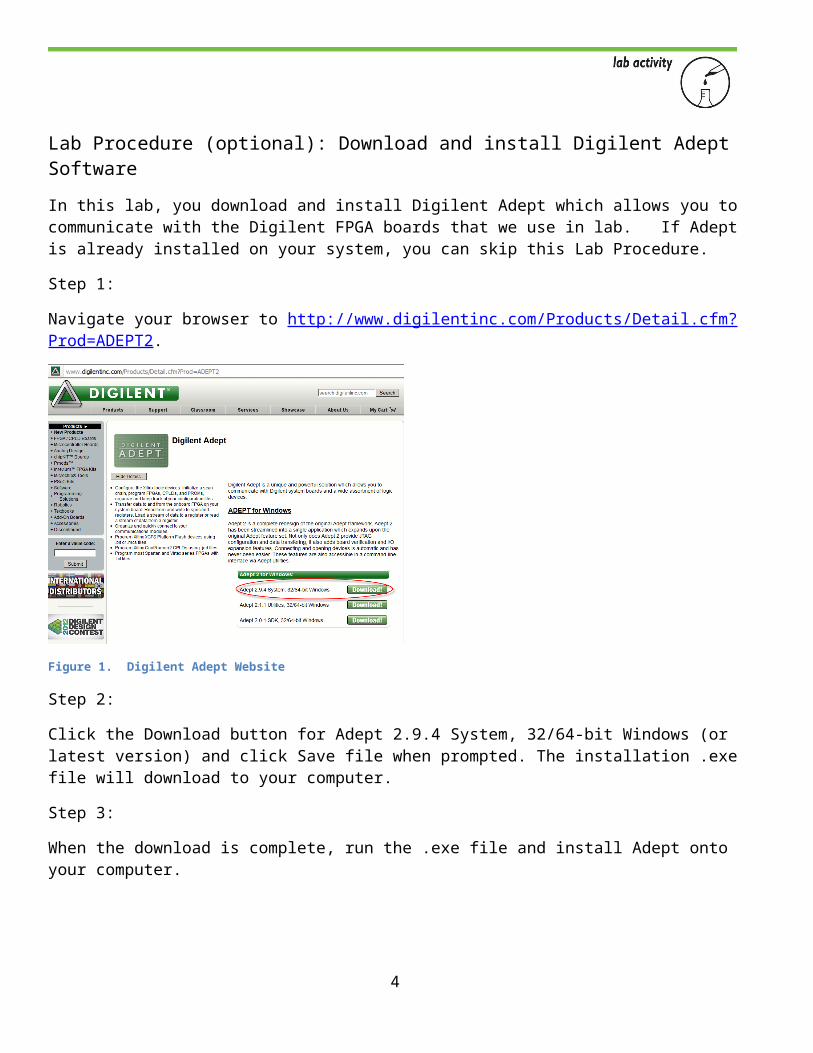
Lab Procedure (optional): Download and install Digilent Adept SoftwareIn this lab, you download and install Digilent Adept which allows you to communicate with the Digilent FPGA boards that we use in lab. If Adept is already installed on your system, you can skip this Lab Procedure.
Step 1:
Navigate your browser to http://www.digilentinc.com/Products/Detail.cfm?Prod=ADEPT2.
Figure 1. Digilent Adept Website
Step 2:
Click the Download button for Adept 2.9.4 System, 32/64-bit Windows (or latest version) and click Save file when prompted. The installation .exe file will download to your computer.
Step 3:
When the download is complete, run the .exe file and install Adept onto your computer.
3
Lab Procedure 1: FPGA Overview
NOTE: We used the Digilent Nexys-3 Xilinx® Spartan 6 XC6LX16-CS324 board. Your board may be a different version or from a different vendor. However, most of the components are similar. If you have a different board, review your board’s documentation.
The Nexys-3 is a powerful digital system design platform built around a Xilinx Spartan 6 FPGA. The advantage of this board is that it is programmed and powered through a USB port. A list of the key features and their location on the board are shown in Figure 2.
Figure 2. Nexys 3, Spartan 6 FPGA
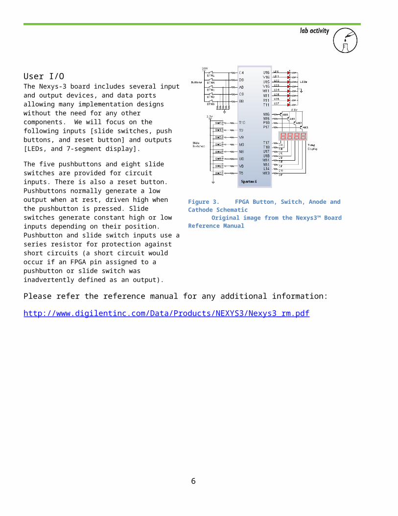
User I/OThe Nexys-3 board includes several input and output devices, and data ports allowing many implementation designs without the need for any other components. We will focus on the following inputs [slide switches, push buttons, and reset button] and outputs [LEDs, and 7-segment display].
The five pushbuttons and eight slide switches are provided for circuit inputs. There is also a reset button. Pushbuttons normally generate a low output when at rest, driven high when the pushbutton is pressed. Slide switches generate constant high or low inputs depending on their position. Pushbutton and slide switch inputs use a series resistor for protection against short circuits (a short circuit would occur if an FPGA pin assigned to a pushbutton or slide switch was inadvertently defined as an output).
Figure 3. FPGA Button, Switch, Anode and Cathode SchematicOriginal image from the Nexys3™ Board Reference Manual
Please refer the reference manual for any additional information:
http://www.digilentinc.com/Data/Products/NEXYS3/Nexys3_rm.pdf
4
PowerPower good LED
Power Select Jumper
Power SwitchAdept USB Port
10/100 Ethernet
VGA Port USB HID Host Port
8 Slide switches8 LEDs Push buttons
USB UART
7-Segment Display
VHDC Connector
Reset Button
MODE Jumper
JTAG Header
Done LED Pmod Connectors

5
Lab Procedure 2: Introduction to Sequence DetectorsIn this lab, we will implement a sequence detector on the NEXYS2 starter board. The sequence detector will look for the input series “10010.” The LED’s will show how much of the series has been detected and when the entire series has been entered an additional LED will come on. Circuit input will be controlled by a reset button, another button that sends a clock pulse and a switch that will enter a ‘1’ or a ‘0’.
When describing the behavior of a sequential logic circuit we talk about the state of the circuit. The state of a sequential circuit is a result of all previous inputs which determines the circuit’s output and future behavior. This is why sequential circuits are often referred to as state machines.
Most sequential circuits (including our sequence detector) use a clock signal to control when the state changes. The inputs of the circuit along with the circuit’s current state provide the information to determine the circuit’s next state. The clock signal then controls the passing of this information to the state memory. The output depends only on the circuit’s state, this is known as a Moore Machine. Figure 4 shows the schematic of a Moore Machine.
Figure 4. Schematic of a Clocked Synchronous State Machine (Moore Machine)
A sequential circuit’s behavior can be shown in a state diagram. The state diagram for our sequence detector is shown in Figure 5. Each circle represents a state and the arrows show the transitions to the next state. Inside each circle are the state name and the value of the output. Along each arrow is the input value that corresponds to that transition.
NOTE: This state diagram illustrates the sequence detector in this tutorial.
6
Figure 5. State Diagram for 5-Bit Sequence 10010

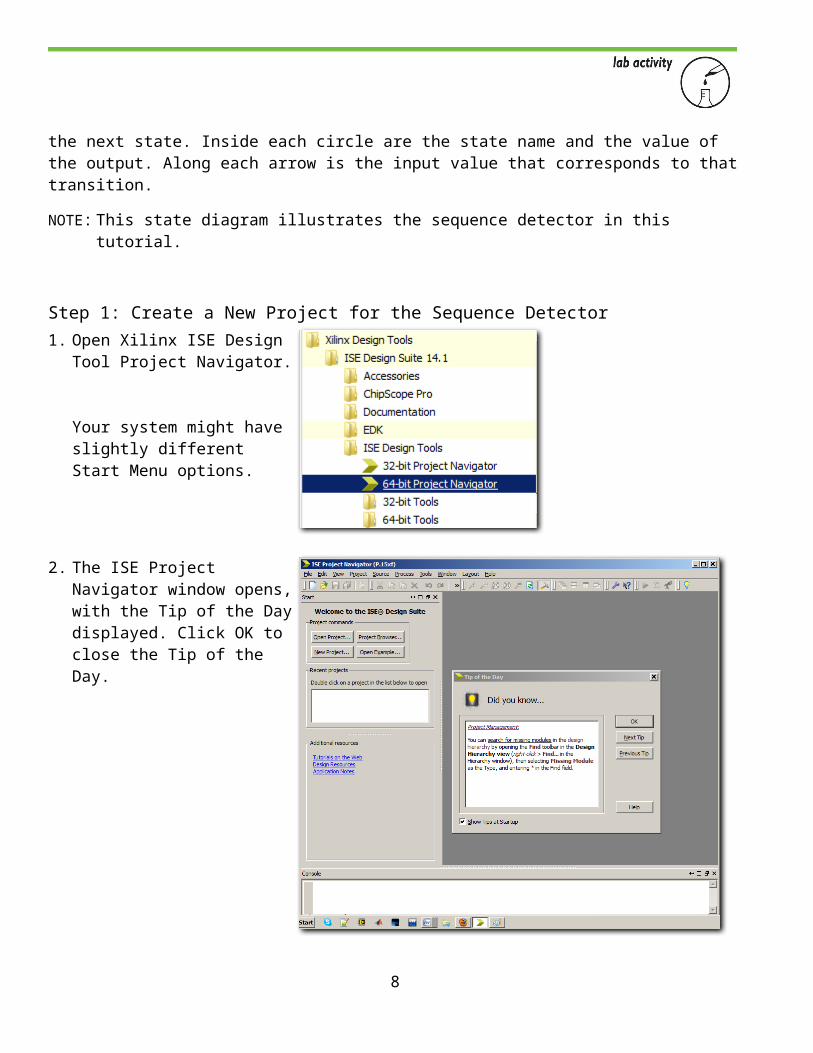
Step 1: Create a New Project for the Sequence Detector1. Open Xilinx ISE Design Tool
Project Navigator.
Your system might have slightly different Start Menu options.
2. The ISE Project Navigator window opens, with the Tip of the Day displayed. Click OK to close the Tip of the Day.
7
3. Start a new project by selecting File New Project from the menu. The New Project Wizard starts.
a. Type LAB8 in the Name text box.
b. Select a location on your computer to save your project files by clicking the ellipsis (…) button to the right of the Location text box.
c. Under Top-level source type, select HDL.
d. Click Next.
The Project Settings dialog box opens.
NOTE: File names must start with a letter. Use underscores ( _ ) for readability. Do not use hyphens (-); although the file name will work, the entity name will not. More on this later.
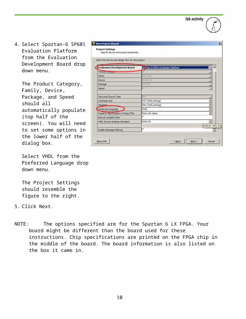
4. Select Spartan-6 SP601 Evaluation Platform from the Evaluation Development Board drop down menu.
The Product Category, Family, Device, Package, and Speed should all automatically populate (top half of the screen). You will need to set some options in the lower half of the dialog box.
Select VHDL from the Preferred Language drop down menu.
The Project Settings should resemble the figure to the right.
8

5. Click Next.
NOTE: The options specified are for the Spartan 6 LX FPGA. Your board might be different than the board used for these instructions. Chip specifications are printed on the FPGA chip in the middle of the board. The board information is also listed on the box it came in.
6. Verify the file type and name are correct in the Project Summary then click Finish to complete the New Project creation process.
NOTE: For this project, the source files have already been created for you. You will add them to the project. Copy the source files into the LAB8 project folder that ISE created. There are five files for this project: top_sequence.vhd, sequence.vhd, sequence_tb.vhd, clockbuffer.vhd, and top_sequence.ucf. The project files are in the lab8.zip file. If you don’t have the zip file you can download it from the COSMIAC website (http://cosmiac.org/Projects_FPGA.html).
7. Using Windows Explorer, extract or move all five files to your project folder.
9
8. Select Project Add Source from the menu or Right-click in the Hierarchy pane and select Add Source from the shortcut menu. The Add Source dialog box opens.
9. Select the five files that were extracted to the project directory earlier. Click the Open button. The Adding Source Files… dialog box opens.
10. Click the OK button to complete the add files process.
NOTE: All five project files display with a green checkmark to the left of the file name. This lets us know that ISE understands the design association of each of the files.
11. The files are added to the LAB8 project. Clicking the Implementation or Simulation options displays the files that were just added.
NOTE: Refer to Labs 1 – 3 for information about the file Hierarchy pane. Recall that when Implementation is selected the UCF file should be below the design file it is associated with. When Simulation is selected, the UUT should be under the associated testbench file.
10

Take some time to look through the .vhd files. They have been notated to help you understand the VHDL code. The layout of the three components is shown in Figure 6.
Figure 6. Structure of top_sequence
Step 2: Run the Simulation12. Select the Simulation pane and Double-click
the testbench – behavior (sequence_tb.vhd) file name. The sequence_tb.vhd file opens in the Workspace.
13. Select the testbench file and double-click on the “Simulate Behavioral Model”.
14. The simulator will start and the Elaborating status will display. Once the simulation is complete the ISim application window will open.
15. Click the Zoom to Full View button , then click Zoom In to better view the simulation.
16. Close the ISim Window and return to the ISE Design Window.
11

Step 3: Review the UCF (User Constraints File)17. In the sources pane,
choose Implementation.
18. Double-click the top_sequence.ucf file in the Processes pane to review the UCF code.
12

Step 4: Program to the FPGA boardTask A: Synthesize, Implement, Map, Place and Route, Generate Bitstream1. Insert the small end of the USB cable into the Adept
USB Port on the FPGA board. Insert the USB end into your computer.
2. Turn on the FPGA board.
NOTE: The display may alternately flash PASS and 128 if the board’s ROM hasn’t been overwritten from the factory.
3. In the Processes Panel, double-click Generate Programming File.
As the program is going through the compile process the compiling the process status icon spins and displays the current process that is running.
The Console Panel also displays textually what is happening.
4. Once the process has stopped running, and there are no errors, either three green checkmarks or a combination of green checkmarks and yellow warnings will display next to the Synthesize, Implement Design, and Generate Programming File processes.
The figure on the right shows the yellow warning symbols. We have warnings because of two issues:
a. The software subscription has lapsed. Not a show stopper.
b. The debouncer is showing as a gated clock. Again, not a show stopper.
13

NOTE: If you have errors you will need to find and fix the errors. You may or many not need to fix warnings. After fixing any errors, re-generate the programming file.
Click the Errors (and/or Warnings) Panel tab to display a list of all errors (and/or warnings) (1).
Clicking the hyperlink (2) of a particular Error (or Warning) will take you to the file and line (3) of the Error (or Warning). Note in the example the semicolon is missing at the end of line 37.
Clicking the hyperlink word Error (4) (or Warning) will display context sensitive information about the particular error/warning.
To re-generate the programming file, right-click on Generate Programming File and select Rerun All.
14

Task B: Implement design to FPGA boardBecause the FPGAs we are working with use a single USB cable for power and PC connection we need to use Digilent Adept to transfer the .bit code to the board.
1. Open Digilent Adept by selecting Start All Programs Digilent Adept Adept.
NOTE: Your system might have slightly different Start Menu options.
2. Choose Nexys3 from the Connect Product drop down menu.
NOTE: If you do not see Nexys3 as an option, check the USB connection to ensure the board is connected to the computer.
3. Click the Browse button. The Open dialog box displays.
4. Navigate to the folder of the Full_Adder project and select the full_adder.bit file.
5. Click the Open button. The file is displayed in the dropdown list next to the FPGA icon.
15

6. Click the Program button. The bit file is programmed to the FPGA board. The green status bar at the bottom of the Adept screen displays the status as the chip is programmed.
7. The program gets downloaded to the FPGA board.
The NEXYS 3 is programmed as a sequence detector for the input series “10010”, and LD0 (U16) should light up. The board will hold this program until the power is turned off, the reset button near the yellow LED is pressed, or you reprogram the board. Experiment with the board:
The .ucf file shows that SW1 (T9) will be used to control the data input. A high switch enters a 1, and a low switch enters a 0.
The .ucf also shows that BTNS (B8) is a button used to control the clock, for example:
To transition from state A to state B:
Flip SW1 high Press BTN0 LD1 (V16) should light up, indicating the transition from state A to state B.
To transition from state B to state C:
Flip SW1 low Press BTN0 LD2 should light up, indicating the transition.
And so on, following the state diagram and the above process until LD5 and LD6 light up. After that the the sequence has come full circle, back to state A. For reference, follow the state diagram in Figure 5.
Acknowledgment:Wakerly, John F. (2006). Digital Design: Principles and Practices. 4th edition. New Jersey: Pearson Prentice Hall.
16


![netserver.aip.orgnetserver.aip.org/.../717388_2_data_set.docx · Web viewsimulation package (VASP) [S1, S2]. The nuclei and core electrons are described by the projector augmented](https://static.fdocuments.in/doc/165x107/5b03edfe7f8b9a89208ce3b7/viewsimulation-package-vasp-s1-s2-the-nuclei-and-core-electrons-are-described.jpg)