
Lab 5: PCB design with EAGLE - Home | EECS @ … · EECS 473-AES Lab 5: PCB design with EAGLE 2...
23
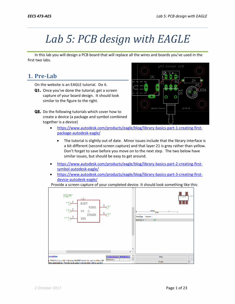
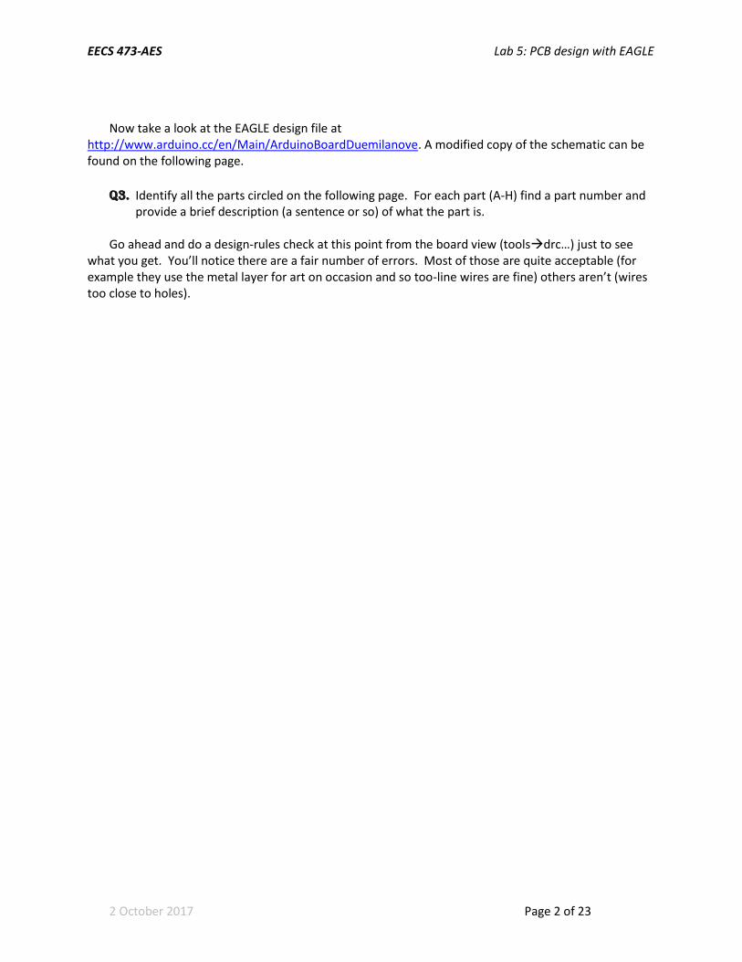
EECS 473-AES Lab 5: PCB design with EAGLE 2 October 2017 Page 1 of 23 Lab 5: PCB design with EAGLE In this lab you will design a PCB board that will replace all the wires and boards you’ve used in the first two labs. 1. Pre-Lab On the website is an EAGLE tutorial. Do it. Q1. Once you’ve done the tutorial, get a screen capture of your board design. It should look similar to the figure to the right. Q2. Do the following tutorials which cover how to create a device (a package and symbol combined together is a device) https://www.autodesk.com/products/eagle/blog/library-basics-part-1-creating-first- package-autodesk-eagle/ The tutorial is slightly out of date. Minor issues include that the library interface is a bit different (second screen capture) and that layer 21 is grey rather than yellow. Don’t forget to save before you move on to the next step. The two below have similar issues, but should be easy to get around. https://www.autodesk.com/products/eagle/blog/library-basics-part-2-creating-first- symbol-autodesk-eagle/ https://www.autodesk.com/products/eagle/blog/library-basics-part-3-creating-first- device-autodesk-eagle/ Provide a screen capture of your completed device. It should look something like this:
Transcript of Lab 5: PCB design with EAGLE - Home | EECS @ … · EECS 473-AES Lab 5: PCB design with EAGLE 2...
EECS 473-AES Lab 5: PCB design with EAGLE
2 October 2017 Page 1 of 23
Lab 5: PCB design with EAGLE In this lab you will design a PCB board that will replace all the wires and boards you’ve used in the
first two labs.
1. Pre-Lab
On the website is an EAGLE tutorial. Do it.
Q1. Once you’ve done the tutorial, get a screen capture of your board design. It should look similar to the figure to the right.
Q2. Do the following tutorials which cover how to create a device (a package and symbol combined together is a device)
https://www.autodesk.com/products/eagle/blog/library-basics-part-1-creating-first-package-autodesk-eagle/
The tutorial is slightly out of date. Minor issues include that the library interface is a bit different (second screen capture) and that layer 21 is grey rather than yellow. Don’t forget to save before you move on to the next step. The two below have similar issues, but should be easy to get around.
https://www.autodesk.com/products/eagle/blog/library-basics-part-2-creating-first-symbol-autodesk-eagle/
https://www.autodesk.com/products/eagle/blog/library-basics-part-3-creating-first-device-autodesk-eagle/
Provide a screen capture of your completed device. It should look something like this:
EECS 473-AES Lab 5: PCB design with EAGLE
2 October 2017 Page 2 of 23
Now take a look at the EAGLE design file at
http://www.arduino.cc/en/Main/ArduinoBoardDuemilanove. A modified copy of the schematic can be found on the following page.
Q3. Identify all the parts circled on the following page. For each part (A-H) find a part number and provide a brief description (a sentence or so) of what the part is.
Go ahead and do a design-rules check at this point from the board view (toolsdrc…) just to see
what you get. You’ll notice there are a fair number of errors. Most of those are quite acceptable (for example they use the metal layer for art on occasion and so too-line wires are fine) others aren’t (wires too close to holes).

EECS 473-AES Lab 5: PCB design with EAGLE
2 October 2017 Page 3 of 23
A B
C
D
E
F
G
H
EECS 473-AES Lab 5: PCB design with EAGLE
2 October 2017 Page 4 of 23
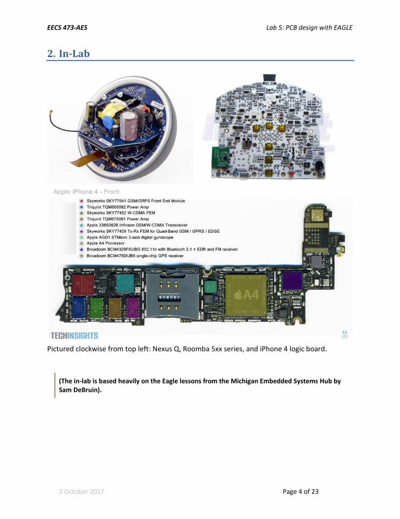
2. In-Lab
Pictured clockwise from top left: Nexus Q, Roomba 5xx series, and iPhone 4 logic board.
(The in-lab is based heavily on the Eagle lessons from the Michigan Embedded Systems Hub by Sam DeBruin).
EECS 473-AES Lab 5: PCB design with EAGLE
2 October 2017 Page 5 of 23
Introduction
In the prelab, you gained experience performing schematic capture and board layout with a simple board in Eagle and looked at a much larger design. In this section, we will be exploring a mid-sized board featuring a simple microcontroller-based system, including a power supply and supporting components such as LEDs.
Part 1: Setting up Eagle
Before we get too far into design, we need to tell EAGLE where to find our projects and
other support files.
● Launch Eagle. You will need to log in (you should have created an account for the
prelab)
● Download the lab5 zip file from the website; Extract the Lab5_files folder.
● In Eagle, select “OptionsDirectories…”.
○ Put the cursor at the end of the “Libraries” textbox. Click “Browse…”.
○ Select the Lab5_files directory (don’t enter it, just select it)
● In the Directories window, place your cursor in the libraries text field and click
“Browse…” and navigate to the folder you made earlier. Select that folder.
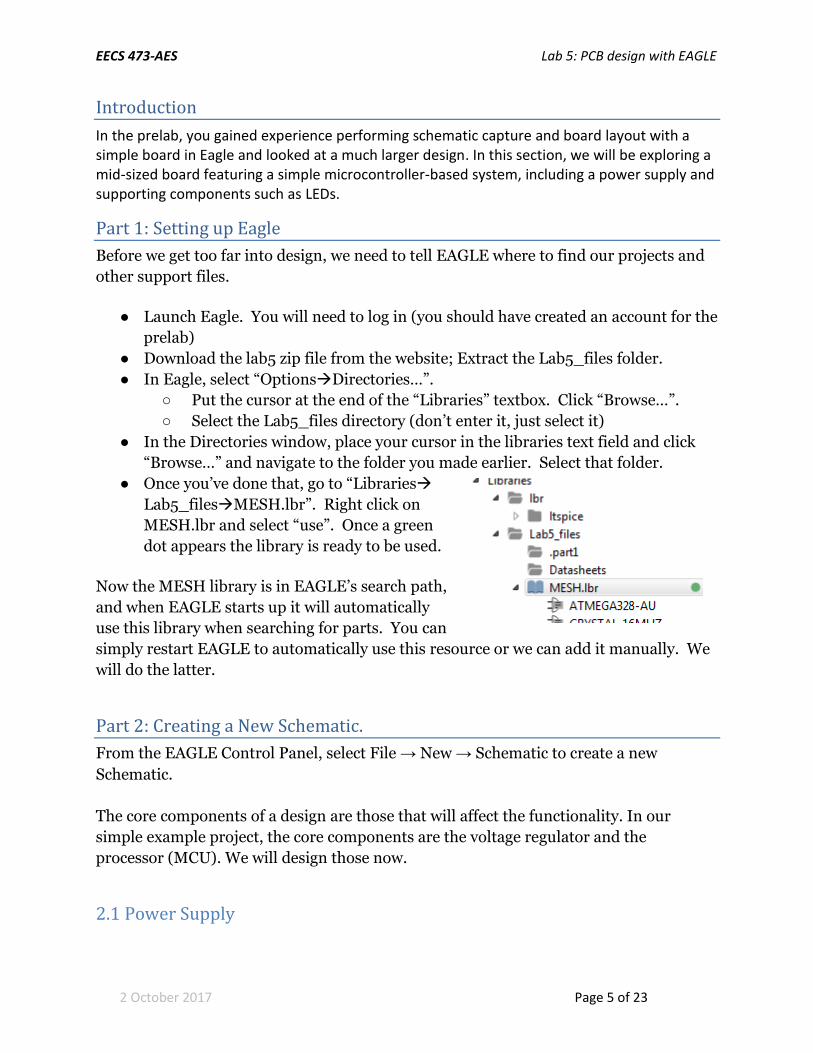
● Once you’ve done that, go to “Libraries
Lab5_filesMESH.lbr”. Right click on
MESH.lbr and select “use”. Once a green
dot appears the library is ready to be used.
Now the MESH library is in EAGLE’s search path,
and when EAGLE starts up it will automatically
use this library when searching for parts. You can
simply restart EAGLE to automatically use this resource or we can add it manually. We
will do the latter.
Part 2: Creating a New Schematic.
From the EAGLE Control Panel, select File → New → Schematic to create a new
Schematic.
The core components of a design are those that will affect the functionality. In our
simple example project, the core components are the voltage regulator and the
processor (MCU). We will design those now.
2.1 Power Supply
EECS 473-AES Lab 5: PCB design with EAGLE
2 October 2017 Page 6 of 23
2.1.1 Place Part
We will start our design by adding our linear dropout regulator (LDO) and the support
components that it requires.
● In the command line (just below the menus at the top), type ‘add’ (no quotes
necessary in the command line) or press enter or press the button. In the add
window you will see a long list of libraries that are in EAGLE’s search path. We
added the MESH library to this path, so we expect that EAGLE will find it. They
are in alphabetical order, so scroll down to find the MESH library and click the
triangle next to it to list the contents of the resource.
● Find the LDO (LM340MPX-5.0/NOPB) in the MESH library. Double click the
LDO or click the ‘OK’ button to add the component to your schematic.
● Place this part in the center of your schematic.
● Press escape to return to the add menu, and then escape to exit the ‘add’ tool.
3.1.2 Add Capacitors
Most voltage regulators will require some capacitors to function. Information on how
many capacitors and of what size are required can be found in the voltage regulator’s
datasheet. Let’s take a look at the LM340MPX-5.0 datasheet. The datasheet is included
in the EAGLE part 1 files you downloaded from the MESH website.
● On the first page, find Figure 1 - ‘Fixed Output Regulation’.
As we can see, we require one 220nF capacitor and one 100nF ceramic capacitor. For
more information on using capacitors in power supplies including capacitor type and
ESR, ask your MESH instructor or refer to the lecture presentation available online.
We’ll add the ceramic caps first.
● Use the ‘add’ tool and find the library named ’rcl’. Expand this library.
● Find the device named ‘C-EU’. Expand this listing.
● Select the part C-EUC0805 and click the ‘OK’ button
● Place this part twice in your schematic, one to either side of the voltage regulator.
See the figure below.
● In the command line type ’value 220nF’ and click on the capacitor on the left
(the input). This can also be accomplished by pressing the (value) button and
entering the values manually.
● Then set the value of the right-hand capacitor to be 100nF.
EECS 473-AES Lab 5: PCB design with EAGLE
2 October 2017 Page 7 of 23
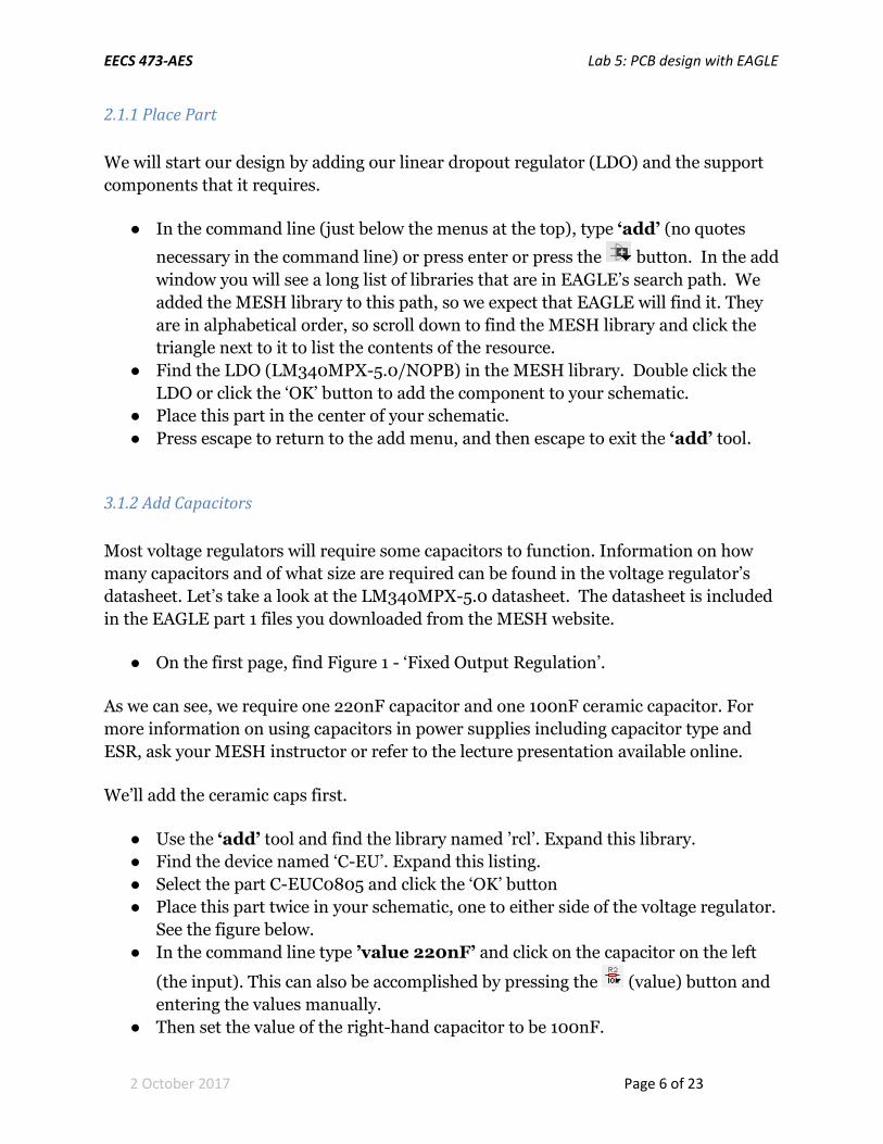
● ‘Add’ a GND symbol by finding the library called ’supply1’ and adding the
symbol GND. Connect the components as shown below. Be sure you have that
“solder dot” which indicates that the crossing nets are in fact connecte.
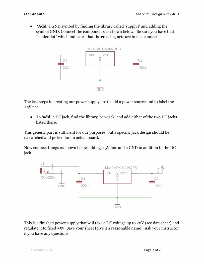
The last steps in creating our power supply are to add a power source and to label the
+5V net.
● To ‘add’ a DC jack, find the library ’con-jack’ and add either of the two DC jacks
listed there.
This generic part is sufficient for our purposes, but a specific jack design should be
researched and picked for an actual board.
Now connect things as shown below adding a 5V line and a GND in addition to the DC
jack.
This is a finished power supply that will take a DC voltage up to 20V (see datasheet) and
regulate it to fixed +5V. Save your sheet (give it a reasonable name). Ask your instructor
if you have any questions.
EECS 473-AES Lab 5: PCB design with EAGLE
2 October 2017 Page 8 of 23
2.2 Processor
With the power supply placed, the next item to place is the processor.
3.2.1 Place Part and Decouple
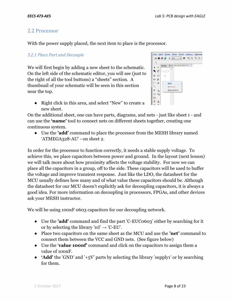
We will first begin by adding a new sheet to the schematic.
On the left side of the schematic editor, you will see (just to
the right of all the tool buttons) a “sheets” section. A
thumbnail of your schematic will be seen in this section
near the top.
● Right click in this area, and select “New” to create a
new sheet.
On the additional sheet, one can have parts, diagrams, and nets - just like sheet 1 - and
can use the ‘name’ tool to connect nets on different sheets together, creating one
continuous system.
● Use the ’add’ command to place the processor from the MESH library named
‘ATMEGA328-AU’ - on sheet 2.
In order for the processor to function correctly, it needs a stable supply voltage. To
achieve this, we place capacitors between power and ground. In the layout (next lesson)
we will talk more about how proximity affects the voltage stability. For now we can
place all the capacitors in a group, off to the side. These capacitors will be used to buffer
the voltage and improve transient response. Just like the LDO, the datasheet for the
MCU usually defines how many and of what value these capacitors should be. Although
the datasheet for our MCU doesn’t explicitly ask for decoupling capacitors, it is always a
good idea. For more information on decoupling in processors, FPGAs, and other devices
ask your MESH instructor.
We will be using 100nF 0603 capacitors for our decoupling network.
● Use the ’add’ command and find the part ’C-EUC0603’ either by searching for it
or by selecting the library ’rcl’ → ’C-EU’.
● Place two capacitors on the same sheet as the MCU and use the ’net’ command to
connect them between the VCC and GND nets. (See figure below)
● Use the ‘value 100nf’ command and click on the capacitors to assign them a
value of 100nF.
● ‘Add’ the ’GND’ and ’+5V’ parts by selecting the library ’supply1’ or by searching
for them.
EECS 473-AES Lab 5: PCB design with EAGLE
2 October 2017 Page 9 of 23
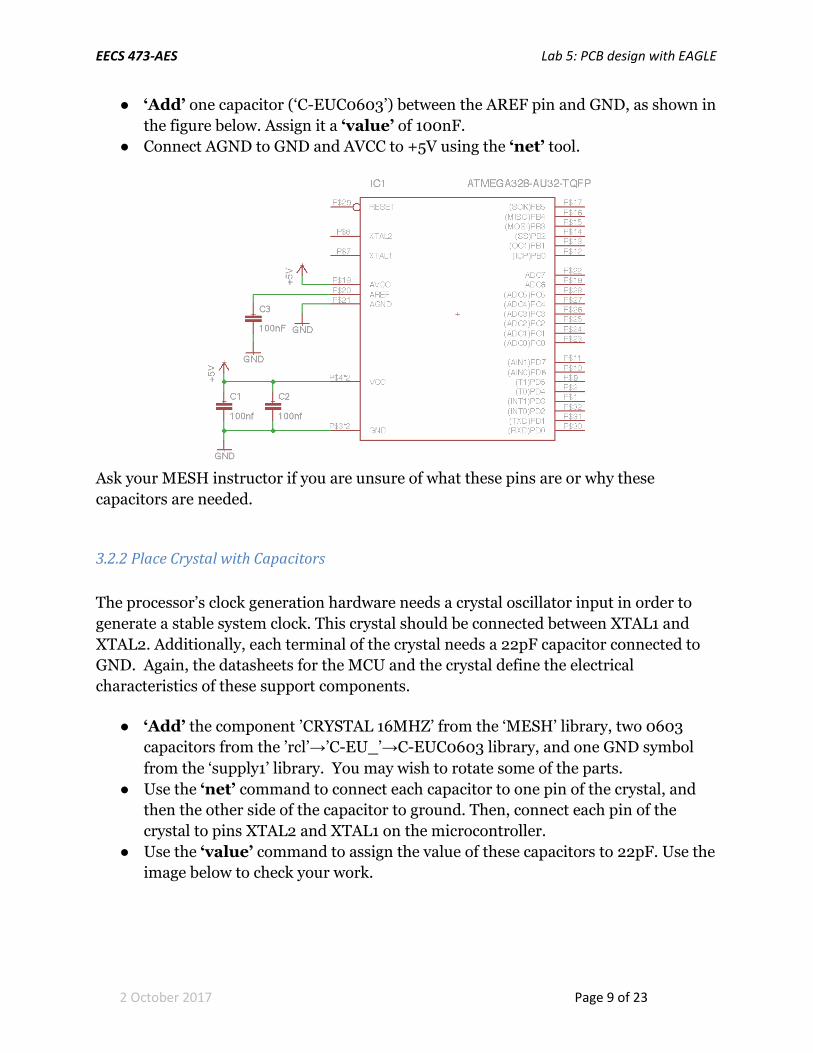
● ‘Add’ one capacitor (‘C-EUC0603’) between the AREF pin and GND, as shown in
the figure below. Assign it a ‘value’ of 100nF.
● Connect AGND to GND and AVCC to +5V using the ‘net’ tool.
Ask your MESH instructor if you are unsure of what these pins are or why these
capacitors are needed.
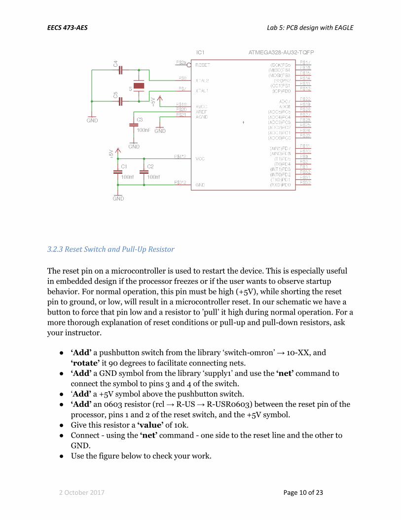
3.2.2 Place Crystal with Capacitors
The processor’s clock generation hardware needs a crystal oscillator input in order to
generate a stable system clock. This crystal should be connected between XTAL1 and
XTAL2. Additionally, each terminal of the crystal needs a 22pF capacitor connected to
GND. Again, the datasheets for the MCU and the crystal define the electrical
characteristics of these support components.
● ‘Add’ the component ’CRYSTAL 16MHZ’ from the ‘MESH’ library, two 0603
capacitors from the ’rcl’→’C-EU_’→C-EUC0603 library, and one GND symbol
from the ‘supply1’ library. You may wish to rotate some of the parts.
● Use the ‘net’ command to connect each capacitor to one pin of the crystal, and
then the other side of the capacitor to ground. Then, connect each pin of the
crystal to pins XTAL2 and XTAL1 on the microcontroller.
● Use the ‘value’ command to assign the value of these capacitors to 22pF. Use the
image below to check your work.
EECS 473-AES Lab 5: PCB design with EAGLE
2 October 2017 Page 10 of 23
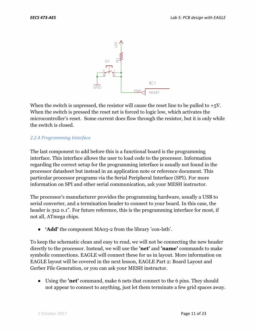
3.2.3 Reset Switch and Pull-Up Resistor
The reset pin on a microcontroller is used to restart the device. This is especially useful
in embedded design if the processor freezes or if the user wants to observe startup
behavior. For normal operation, this pin must be high (+5V), while shorting the reset
pin to ground, or low, will result in a microcontroller reset. In our schematic we have a
button to force that pin low and a resistor to ’pull’ it high during normal operation. For a
more thorough explanation of reset conditions or pull-up and pull-down resistors, ask
your instructor.
● ‘Add’ a pushbutton switch from the library ‘switch-omron’ → 10-XX, and
‘rotate’ it 90 degrees to facilitate connecting nets.
● ‘Add’ a GND symbol from the library ‘supply1’ and use the ‘net’ command to
connect the symbol to pins 3 and 4 of the switch.
● ‘Add’ a +5V symbol above the pushbutton switch.
● ‘Add’ an 0603 resistor (rcl → R-US → R-USR0603) between the reset pin of the
processor, pins 1 and 2 of the reset switch, and the +5V symbol.
● Give this resistor a ‘value’ of 10k.
● Connect - using the ‘net’ command - one side to the reset line and the other to
GND.
● Use the figure below to check your work.
EECS 473-AES Lab 5: PCB design with EAGLE
2 October 2017 Page 11 of 23
When the switch is unpressed, the resistor will cause the reset line to be pulled to +5V.
When the switch is pressed the reset net is forced to logic low, which activates the
microcontroller’s reset. Some current does flow through the resistor, but it is only while
the switch is closed.
2.2.4 Programming Interface
The last component to add before this is a functional board is the programming
interface. This interface allows the user to load code to the processor. Information
regarding the correct setup for the programming interface is usually not found in the
processor datasheet but instead in an application note or reference document. This
particular processor programs via the Serial Peripheral Interface (SPI). For more
information on SPI and other serial communication, ask your MESH instructor.
The processor’s manufacturer provides the programming hardware, usually a USB to
serial converter, and a termination header to connect to your board. In this case, the
header is 3x2 0.1”. For future reference, this is the programming interface for most, if
not all, ATmega chips.
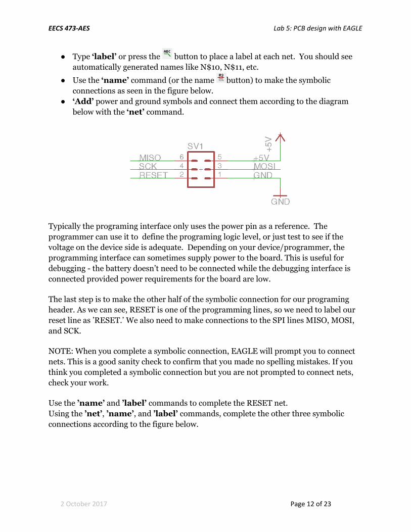
● ‘Add’ the component MA03-2 from the library ’con-lstb’.
To keep the schematic clean and easy to read, we will not be connecting the new header
directly to the processor. Instead, we will use the ’net’ and ’name’ commands to make
symbolic connections. EAGLE will connect these for us in layout. More information on
EAGLE layout will be covered in the next lesson, EAGLE Part 2: Board Layout and
Gerber File Generation, or you can ask your MESH instructor.
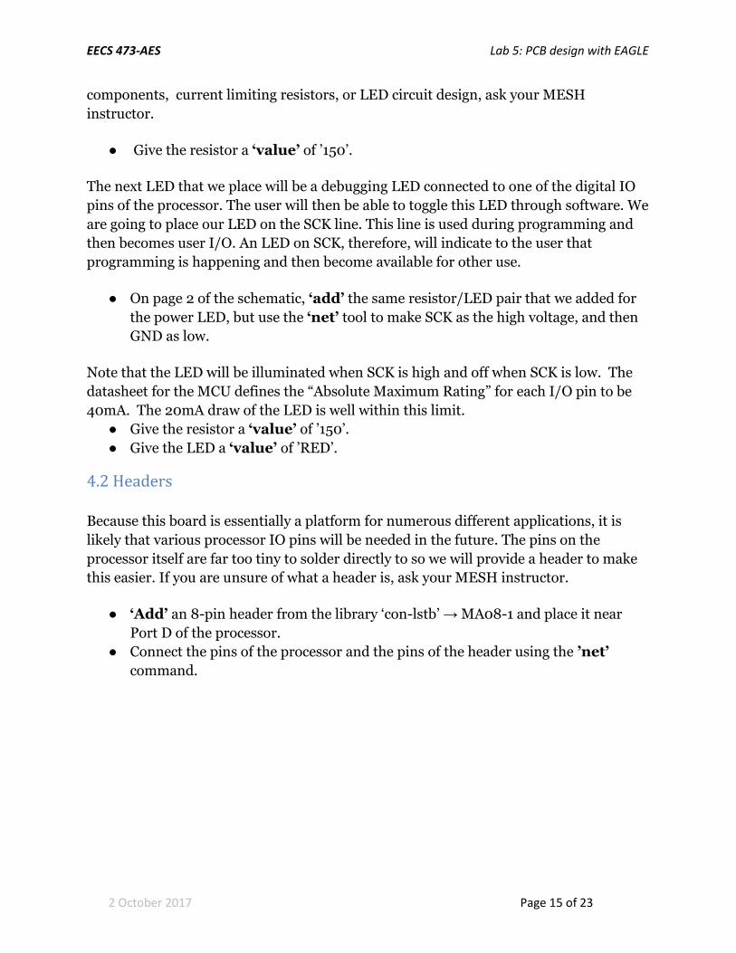
● Using the ’net’ command, make 6 nets that connect to the 6 pins. They should
not appear to connect to anything, just let them terminate a few grid spaces away.
EECS 473-AES Lab 5: PCB design with EAGLE
2 October 2017 Page 12 of 23
● Type ‘label’ or press the button to place a label at each net. You should see
automatically generated names like N$10, N$11, etc.
● Use the ‘name’ command (or the name button) to make the symbolic
connections as seen in the figure below.
● ‘Add’ power and ground symbols and connect them according to the diagram
below with the ‘net’ command.
Typically the programing interface only uses the power pin as a reference. The
programmer can use it to define the programing logic level, or just test to see if the
voltage on the device side is adequate. Depending on your device/programmer, the
programming interface can sometimes supply power to the board. This is useful for
debugging - the battery doesn’t need to be connected while the debugging interface is
connected provided power requirements for the board are low.
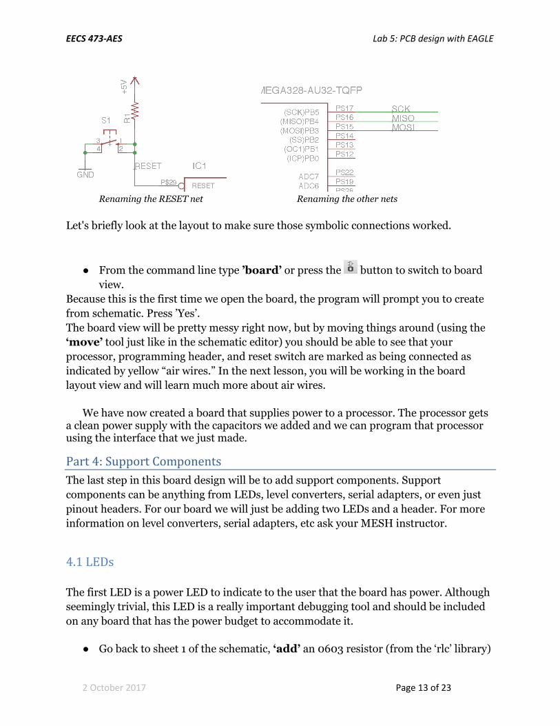
The last step is to make the other half of the symbolic connection for our programing
header. As we can see, RESET is one of the programming lines, so we need to label our
reset line as ’RESET.’ We also need to make connections to the SPI lines MISO, MOSI,
and SCK.
NOTE: When you complete a symbolic connection, EAGLE will prompt you to connect
nets. This is a good sanity check to confirm that you made no spelling mistakes. If you
think you completed a symbolic connection but you are not prompted to connect nets,
check your work.
Use the ’name’ and ’label’ commands to complete the RESET net.
Using the ’net’, ’name’, and ’label’ commands, complete the other three symbolic
connections according to the figure below.
EECS 473-AES Lab 5: PCB design with EAGLE
2 October 2017 Page 13 of 23
Renaming the RESET net Renaming the other nets
Let's briefly look at the layout to make sure those symbolic connections worked.
● From the command line type ’board’ or press the button to switch to board
view.
Because this is the first time we open the board, the program will prompt you to create
from schematic. Press ’Yes’.
The board view will be pretty messy right now, but by moving things around (using the
‘move’ tool just like in the schematic editor) you should be able to see that your
processor, programming header, and reset switch are marked as being connected as
indicated by yellow “air wires.” In the next lesson, you will be working in the board
layout view and will learn much more about air wires.
We have now created a board that supplies power to a processor. The processor gets a clean power supply with the capacitors we added and we can program that processor using the interface that we just made.
Part 4: Support Components
The last step in this board design will be to add support components. Support
components can be anything from LEDs, level converters, serial adapters, or even just
pinout headers. For our board we will just be adding two LEDs and a header. For more
information on level converters, serial adapters, etc ask your MESH instructor.
4.1 LEDs
The first LED is a power LED to indicate to the user that the board has power. Although
seemingly trivial, this LED is a really important debugging tool and should be included
on any board that has the power budget to accommodate it.
● Go back to sheet 1 of the schematic, ‘add’ an 0603 resistor (from the ‘rlc’ library)

EECS 473-AES Lab 5: PCB design with EAGLE
2 October 2017 Page 14 of 23
● ‘Add’ an LED from the library ’led’ ->’LED’ -> LEDCHIP-LED0603.
● Give the LED a ‘value’ of ’GREEN’.
● Also add a +5V symbol and GND symbol from the supply1 library.
● Use the ‘net’ tool to connect the 4 symbols in series. The path of conventional
current should flow as follows +5V -> Resistor -> LED -> GND, as to the right in
the figure below.
Now we need to decide what value to give the current limiting resistor. If the value of
the current limiting resistor is too high, the LED will be dim. If the value of the current
limiting resistor is too low, the LED will draw too much power and burn out. To
determine the correct value we need to do some research and math. Let’s take a look at
the datasheet for the LED (provided in the support files form the MESH website).
We are looking for two pieces of data, forward voltage drop and forward current. On
page 2 of 5 in the table “Electrical / Optical Characteristics” note that the typical voltage
drop is 2.1V when forward current is 20mA.
Now we have our data, now let’s do the math. We know the the current through the
LED is 20mA, so the current through the resistor must be the same. We know that the
voltage for the entire system is 5V and the voltage drop across the LED is 2.1V, this
means that the remaining voltage drop must be over the resistor (2.9V.) Now use Ohms
Law to calculate the value of the resistor. V = I*R, or rearranged, R = V/I = 2.9/0.02 =
145 Ohms. 145 is not a standard resistor value, so we round up to the nearest standard
value (150 Ohms.)
Another aspect to consider is the power dissipated by the current limiting resistor.
Recall that Power = V*I. Our resistor will be dissipating 2.9*0.02 = 0.058 watts. Typical
0603 resistors are 0.1W rated, so this design will work. If we wanted a smaller resistor
(with lower power rating) or higher current (brighter LED), then we would have to
choose components that match specifications. For more information about choosing
EECS 473-AES Lab 5: PCB design with EAGLE
2 October 2017 Page 15 of 23
components, current limiting resistors, or LED circuit design, ask your MESH
instructor.
● Give the resistor a ‘value’ of ’150’.
The next LED that we place will be a debugging LED connected to one of the digital IO
pins of the processor. The user will then be able to toggle this LED through software. We
are going to place our LED on the SCK line. This line is used during programming and
then becomes user I/O. An LED on SCK, therefore, will indicate to the user that
programming is happening and then become available for other use.
● On page 2 of the schematic, ‘add’ the same resistor/LED pair that we added for
the power LED, but use the ‘net’ tool to make SCK as the high voltage, and then
GND as low.
Note that the LED will be illuminated when SCK is high and off when SCK is low. The
datasheet for the MCU defines the “Absolute Maximum Rating” for each I/O pin to be
40mA. The 20mA draw of the LED is well within this limit.
● Give the resistor a ‘value’ of ’150’.
● Give the LED a ‘value’ of ’RED’.
4.2 Headers
Because this board is essentially a platform for numerous different applications, it is
likely that various processor IO pins will be needed in the future. The pins on the
processor itself are far too tiny to solder directly to so we will provide a header to make
this easier. If you are unsure of what a header is, ask your MESH instructor.
● ‘Add’ an 8-pin header from the library ‘con-lstb’ → MA08-1 and place it near
Port D of the processor.
● Connect the pins of the processor and the pins of the header using the ’net’
command.
EECS 473-AES Lab 5: PCB design with EAGLE
2 October 2017 Page 16 of 23
Naming and labeling these nets is optional but may be useful during layout.
Part 5: Error Checking
The last step in the schematic process is to run the error checker. This can be run at any
time and is a good way to check your work. Note that it will not catch all errors, just
some, but at least it is a good place to start.
In the command line, type ’erc’, click on the ERC icon, or go to Tools → ERC...
If you followed the part of a lesson correctly, you should have a few warnings about
value - these should largely be ignored. Make sure you fix all errors and at least
understand all the warnings. If you have questions, ask your instructor.
G1. Have your GSI look over your schematic.
Part 6: Initialize and Outline Board
Type 'board' or press the button. If this is the first time opening the board, the program will prompt you to create it. Using either the 'move' command or the 'info' command, change the dimensions of the board outline (layer 20 - Dimension) to 2.6" x 1" centered at the origin. Make sure the width of the board outline wires is '0'.
EECS 473-AES Lab 5: PCB design with EAGLE
2 October 2017 Page 17 of 23
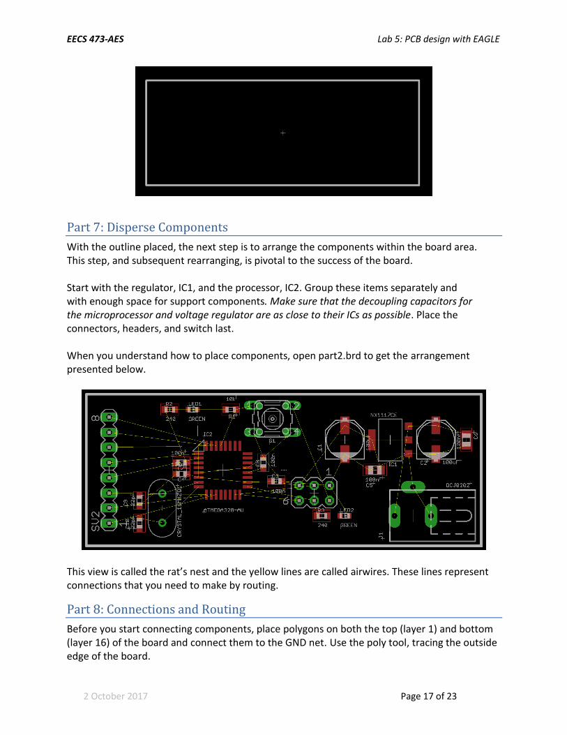
Part 7: Disperse Components
With the outline placed, the next step is to arrange the components within the board area. This step, and subsequent rearranging, is pivotal to the success of the board. Start with the regulator, IC1, and the processor, IC2. Group these items separately and with enough space for support components. Make sure that the decoupling capacitors for the microprocessor and voltage regulator are as close to their ICs as possible. Place the connectors, headers, and switch last. When you understand how to place components, open part2.brd to get the arrangement presented below.
This view is called the rat’s nest and the yellow lines are called airwires. These lines represent connections that you need to make by routing.
Part 8: Connections and Routing
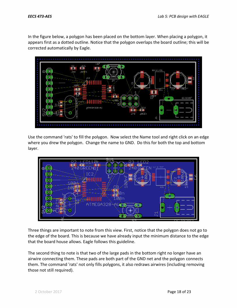
Before you start connecting components, place polygons on both the top (layer 1) and bottom (layer 16) of the board and connect them to the GND net. Use the poly tool, tracing the outside edge of the board.
EECS 473-AES Lab 5: PCB design with EAGLE
2 October 2017 Page 18 of 23
In the figure below, a polygon has been placed on the bottom layer. When placing a polygon, it appears first as a dotted outline. Notice that the polygon overlaps the board outline; this will be corrected automatically by Eagle.
Use the command 'rats' to fill the polygon. Now select the Name tool and right click on an edge where you drew the polygon. Change the name to GND. Do this for both the top and bottom layer.
Three things are important to note from this view. First, notice that the polygon does not go to the edge of the board. This is because we have already input the minimum distance to the edge that the board house allows. Eagle follows this guideline. The second thing to note is that two of the large pads in the bottom right no longer have an airwire connecting them. These pads are both part of the GND net and the polygon connects them. The command 'rats' not only fills polygons, it also redraws airwires (including removing those not still required).

EECS 473-AES Lab 5: PCB design with EAGLE
2 October 2017 Page 19 of 23
The final thing to note from this view is the thermals. If you look closely at the aforementioned GND pins or the GND pin of the programming header (enlarged below) you will notice that the GND plane doesn't connect to the hole all the way around.
Instead, four small copper areas connect to the rest of the GND plane. This allows the pin to be soldered without the iron's heat being wicked away to other parts of the board, potentially causing damage. Practice routing a few of the airwires. Once you get the hang of routing, move on to the next section. You will be given an opportunity to complete the board at the end of the lesson.
Part 9: Gerber Files
See https://www.autodesk.com/products/eagle/blog/gerber-nc-drill-pcb-manufacturing-basics-1/. Generate your Gerber files and drill hole file from the design you’ve done in this lab.
Part 10: Self Check and Final Touches
For this self-check assignment, finish routing the board started during the lesson. The following images with their captions detail a few areas of the board and the key items to consider when working in these areas.
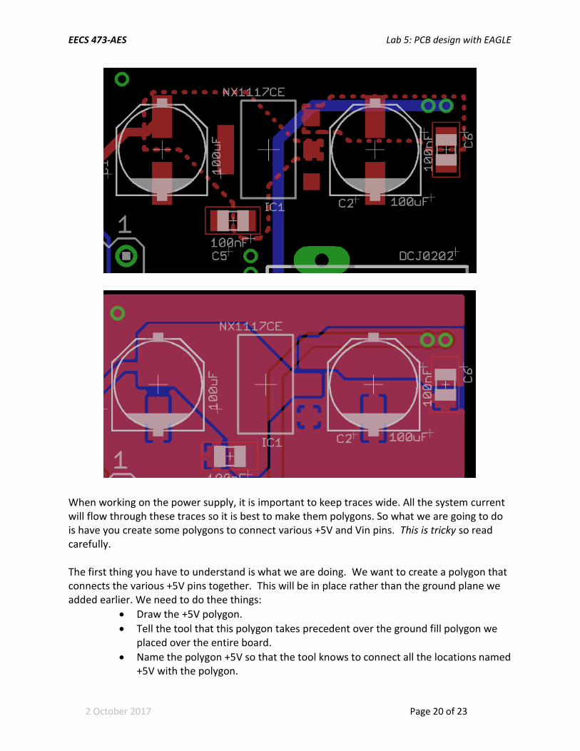
10.1 Power Supply
EECS 473-AES Lab 5: PCB design with EAGLE
2 October 2017 Page 20 of 23
When working on the power supply, it is important to keep traces wide. All the system current will flow through these traces so it is best to make them polygons. So what we are going to do is have you create some polygons to connect various +5V and Vin pins. This is tricky so read carefully. The first thing you have to understand is what we are doing. We want to create a polygon that connects the various +5V pins together. This will be in place rather than the ground plane we added earlier. We need to do thee things:
Draw the +5V polygon.
Tell the tool that this polygon takes precedent over the ground fill polygon we placed over the entire board.
Name the polygon +5V so that the tool knows to connect all the locations named +5V with the polygon.

EECS 473-AES Lab 5: PCB design with EAGLE
2 October 2017 Page 21 of 23
Drawing the polygon is easy. But first, let’s change the ground polygon on layer 1 to give it a lower priority. Click on the edge of where you drew the polygon (not where it is). Be sure you are getting the one on the top of the board (you may want to turn off the back of the board (layer 16). Change the polygon’s rank to 2 (or higher).
Now draw the polygon that includes the various +5V signals. Be sure it’s rank is 1 (so it has higher priority, rank is seen just below the top menu). Be sure to include the +5V pins (you can get other pins too, it won’t matter as the tool will isolate them from your +5V polygon automatically). Now use the name tool, select this new polygon (again, from the edge of the polygon) and change its name to +5V. You should notice that the various +5V signals all are now connected via the polygon.
Do the same for the Vin signals. .
10.2 ATmega

EECS 473-AES Lab 5: PCB design with EAGLE
2 October 2017 Page 22 of 23
As seen in these figures, the organization of components is critical. Place decoupling capacitors as close to their IC as possible. The crystal is of secondary importance to those capacitors and should be placed very near the microcontroller as well.
10.3 Button
10.4 Connectors

EECS 473-AES Lab 5: PCB design with EAGLE
2 October 2017 Page 23 of 23
G2. Show your board layout to your GSI. Be able to justify the decisions you’ve made.
G3. Create a zipfile of your Gerber files and drill hole file you’d need for the manufacture of your board. Show your GSI.
3. Post-lab
Q1. Read https://www.autodesk.com/products/eagle/blog/length-match-high-speed-nets/. Write a paragraph explaining what you learned.
Q2. Read https://www.autodesk.com/products/eagle/blog/every-layer-explained-autodesk-eagle/. What is a layer? Why do so many exist?
Q3. Go to https://www.autodesk.com/products/eagle/blog/. Filter with “Eagle University”. Pick one article that hasn’t been mentioned in this assignment. Read it and write a paragraph explaining what you learned. Notice the “See More” button.


![Designing a Simple Printed Circuit Board with EAGLE Note [PCB DESIGN WITH EAGLE] Kevin Gladstone | ECE480 Spring 2012 1 Designing a Simple Printed Circuit Board with EAGLE Kevin Gladstone](https://static.fdocuments.in/doc/165x107/5b46b3b37f8b9a824f8b68cf/designing-a-simple-printed-circuit-board-with-note-pcb-design-with-eagle-kevin.jpg)