Lab 3 page 1 ENT-DIGI-210 Lab 3 Notes ©Paul Godin Updated September 2007.
23
Lab 3 page 1 ENT-DIGI-210 Lab 3 Notes ©Paul Godin Updated September 2007
-
Upload
leonard-copeland -
Category
Documents
-
view
219 -
download
0
Transcript of Lab 3 page 1 ENT-DIGI-210 Lab 3 Notes ©Paul Godin Updated September 2007.

Lab 3 page 1
ENT-DIGI-210Lab 3 Notes
©Paul GodinUpdated September 2007
Lab 3 page 2
Digital Logic Chips
Basic Chip Configuration
Lab 3 page 3
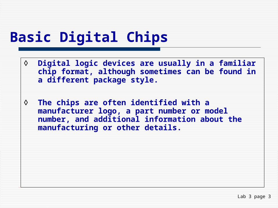
Basic Digital Chips
◊ Digital logic devices are usually in a familiar chip format, although sometimes can be found in a different package style.
◊ The chips are often identified with a manufacturer logo, a part number or model number, and additional information about the manufacturing or other details.
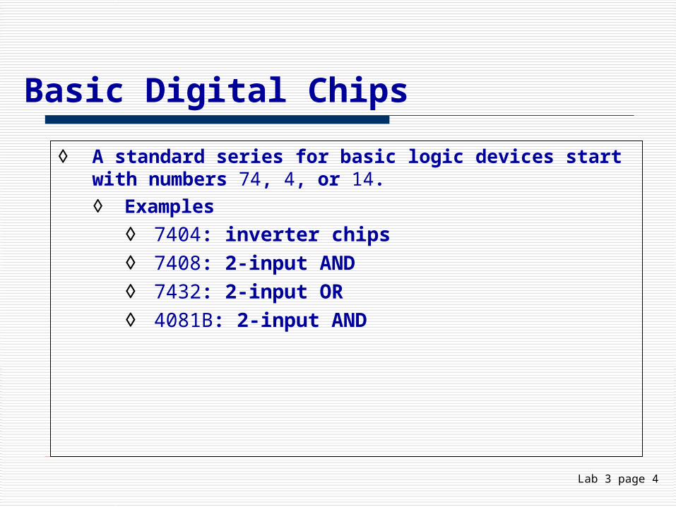
Lab 3 page 4
Basic Digital Chips
◊ A standard series for basic logic devices start with numbers 74, 4, or 14.◊ Examples
◊ 7404: inverter chips◊ 7408: 2-input AND◊ 7432: 2-input OR◊ 4081B: 2-input AND

Lab 3 page 5
Basic Digital Chips
◊ The naming structure (nomenclature) of the devices differs between manufacturers but most follow a common practice for naming their devices (this is called a defacto standard).
◊ Manufacturers publish nomenclature information on their web sites.

Lab 3 page 6
Chip information
Information on this IC:
Second Line= Device Description
DM 74 = Device Family08 = Device TypeN = Packaging (moulded DIP)
First Line = Manufacture Information
M = Wafer made in USAP = Assembled in Malaysia9 = last number of year03 = month of manufacture0V = Die Run Code
National Semiconductor (http://www.advanced-tech.com/ic_logos/ic_logos.htm)
Other information available from http://www.national.com/quality/marking_conventions.html
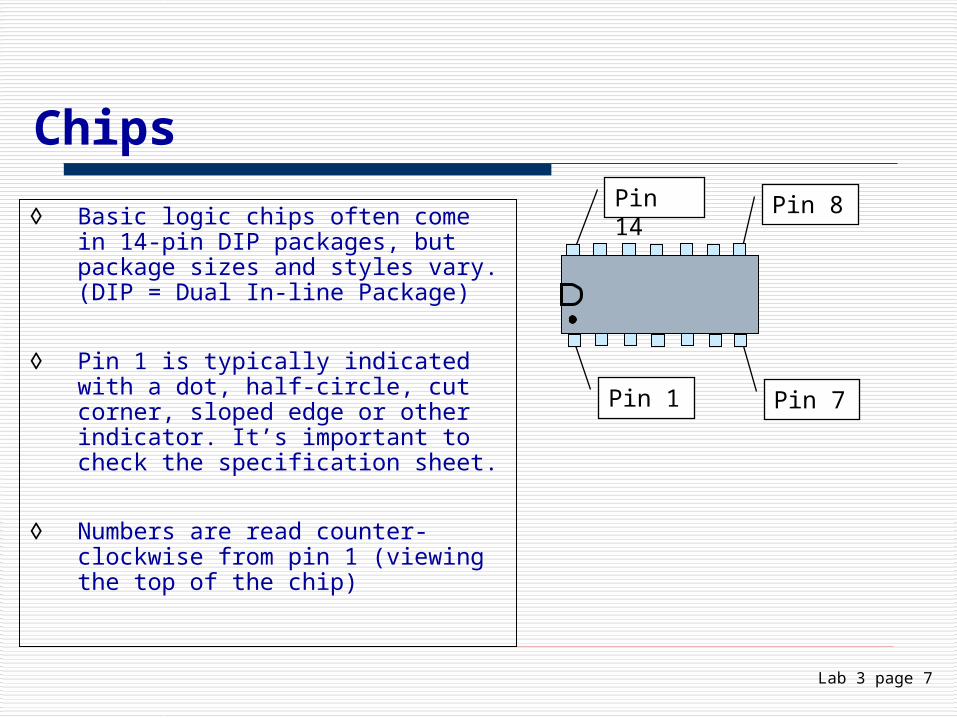
Lab 3 page 7
Chips
◊ Basic logic chips often come in 14-pin DIP packages, but package sizes and styles vary. (DIP = Dual In-line Package)
◊ Pin 1 is typically indicated with a dot, half-circle, cut corner, sloped edge or other indicator. It’s important to check the specification sheet.
◊ Numbers are read counter-clockwise from pin 1 (viewing the top of the chip)
Pin 1 Pin 7
Pin 14 Pin 8

Lab 3 page 8
Chips – Specification Sheet
Diagram from http://www.ti.com
Voltage
Ground
The voltage and ground pins must be connected for the device to function. Check the specification sheet for the Vcc and GND pins.

Lab 3 page 9
Logic Diagram Labels

Lab 3 page 10
Labelling a Diagram
Step 1: Design the circuitStep 2: Add component labels
Changing the component labels in EWB:•Right-click on the component•Select “Component Properties”•Choose:
• “Display” to remove extra labels
• “Label” to add a label• “Value” to change the label
on a switch
Lab 3 page 11
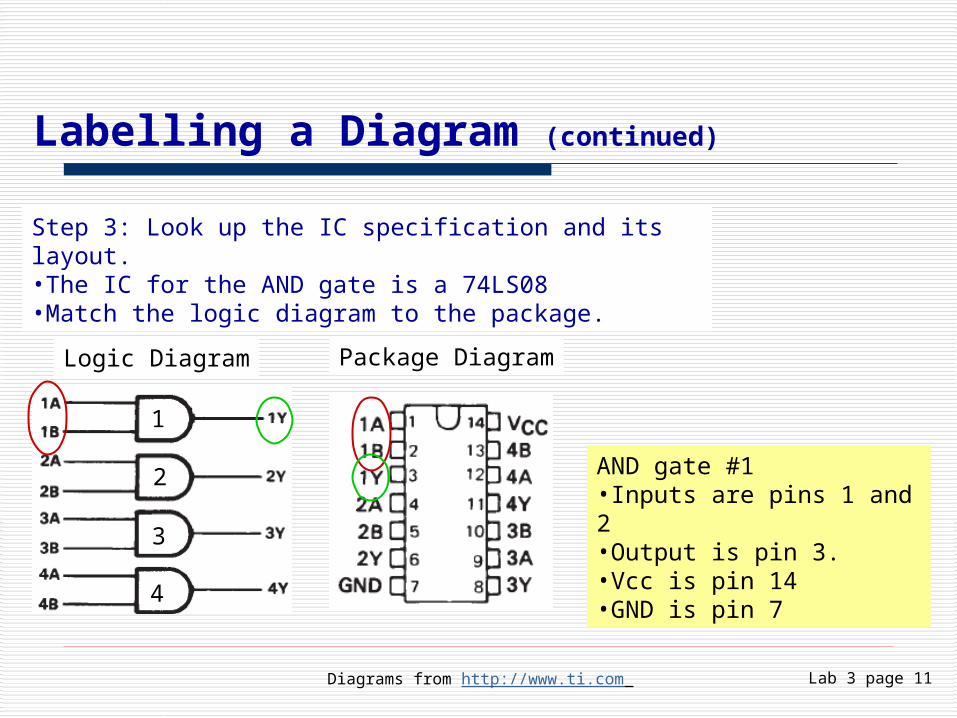
Labelling a Diagram (continued)
Step 3: Look up the IC specification and its layout. •The IC for the AND gate is a 74LS08•Match the logic diagram to the package.
Diagrams from http://www.ti.com
Logic Diagram Package Diagram
1
2
3
4
AND gate #1 •Inputs are pins 1 and 2•Output is pin 3.•Vcc is pin 14•GND is pin 7
Lab 3 page 12
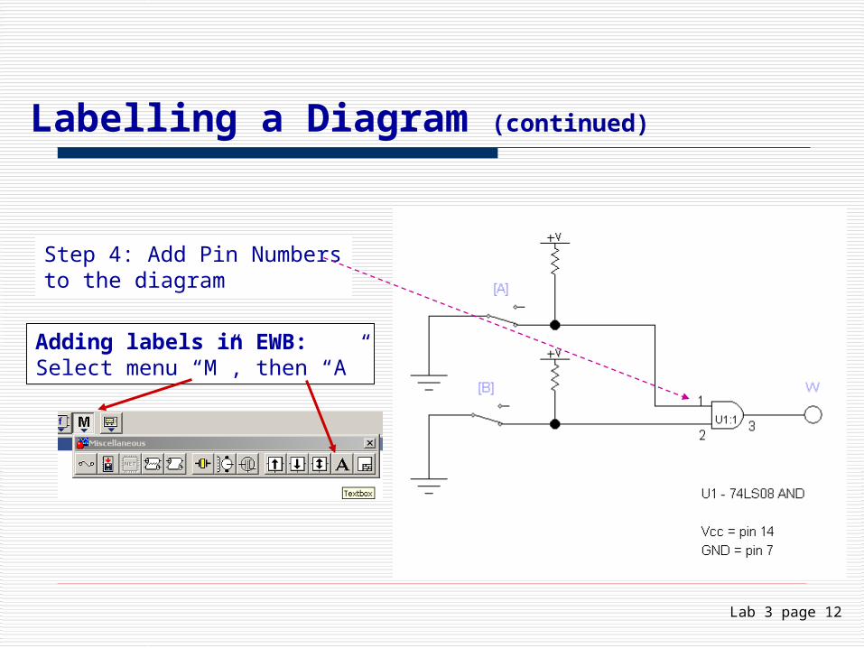
Labelling a Diagram (continued)
Step 4: Add Pin Numbers to the diagram
Adding labels in EWB:Select menu “M”, then “A”

Lab 3 page 13
Chip label U1:1 where:• U1 is the chip• :1 is the number of the
gate within the chip
Labelling a Diagram (continued)
Step 5: Add chip labels and Vcc/GND pins

Lab 3 page 14
Example of a Properly Labelled diagram
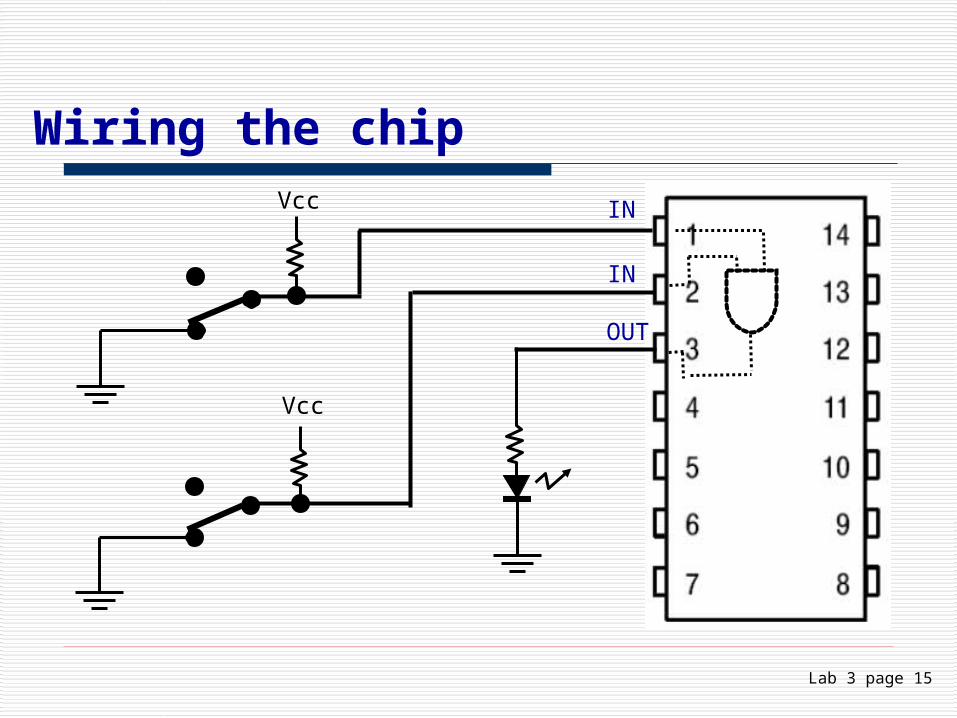
Lab 3 page 15
Wiring the chipVcc
Vcc
IN
IN
OUT

Lab 3 page 16
Steering or Control Gates
Lab 3 page 17
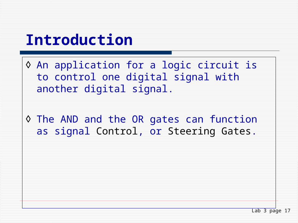
Introduction
◊ An application for a logic circuit is to control one digital signal with another digital signal.
◊ The AND and the OR gates can function as signal Control, or Steering Gates.
Lab 3 page 18
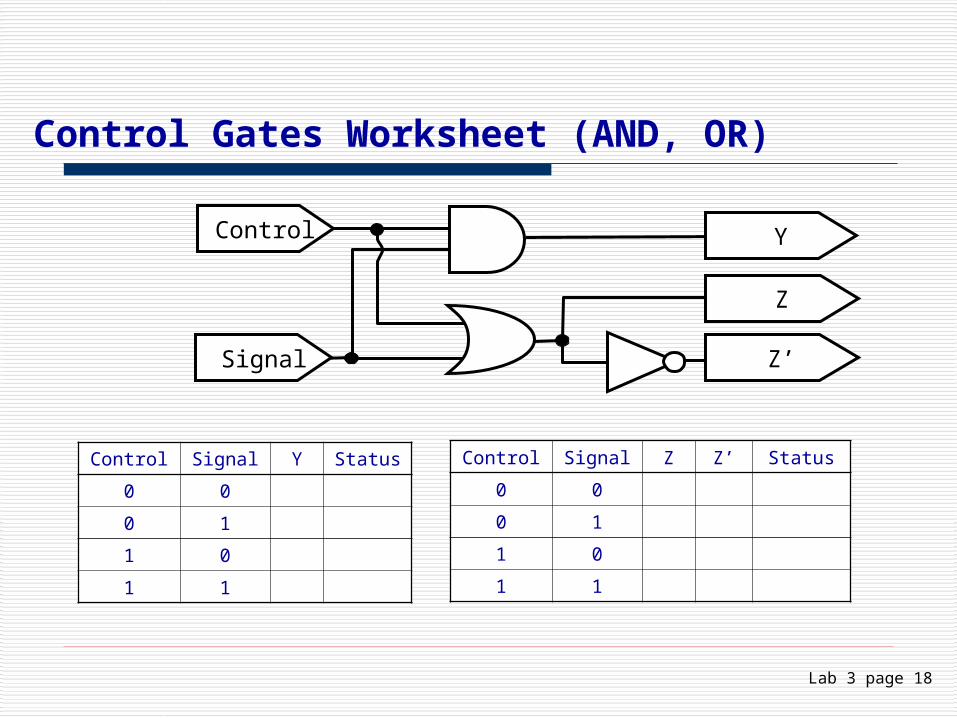
Control Gates Worksheet (AND, OR)
Control Signal Y Status
0 0
0 1
1 0
1 1
Control Signal Z Z’ Status
0 0
0 1
1 0
1 1
Control
Signal
Y
Z
Z’
Lab 3 page 19
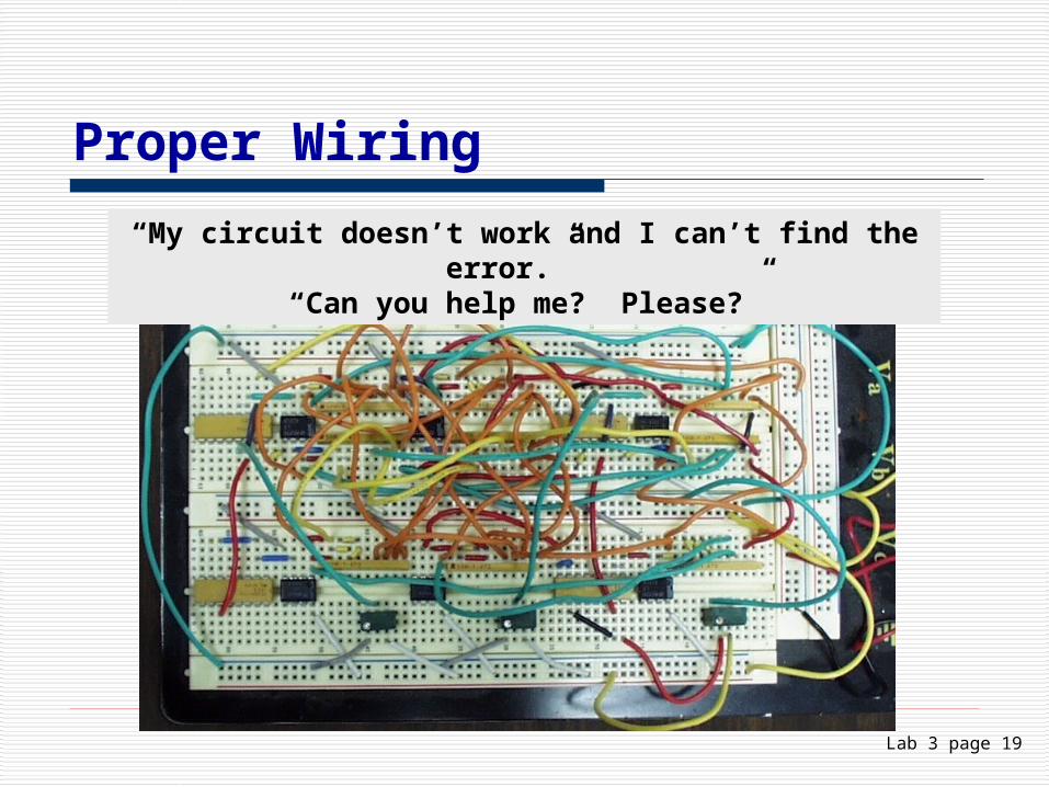
Proper Wiring
“My circuit doesn’t work and I can’t find the error.” “Can you help me? Please?”

Lab 3 page 20Features of a properly-wired circuit
RED reserved for Vcc connections
BLACK reserved for GND Connection
Wires routed around the IC
Wires the proper length
Wires routed along horizontal
and vertical plane
Little or no exposed
conductor
IC is fully visible and accessible
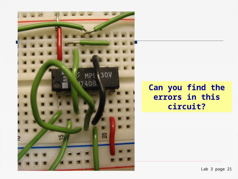
Lab 3 page 21
Can you find the errors in this circuit?
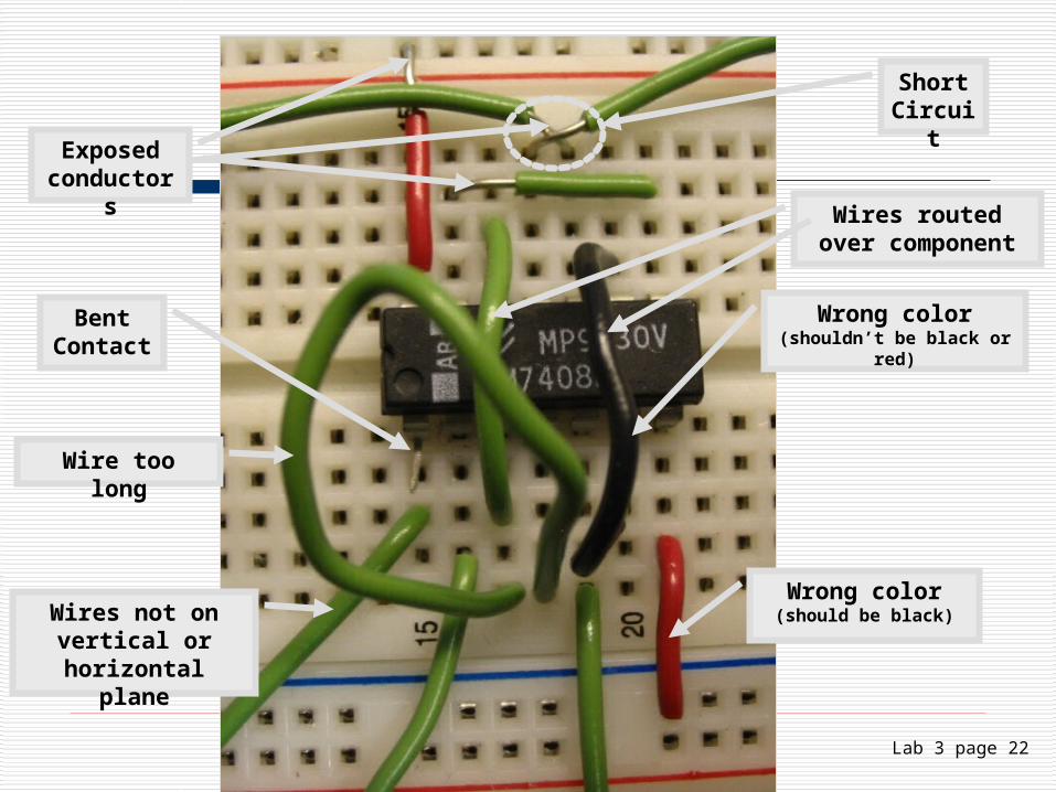
Lab 3 page 22
Exposed conductors
Short Circuit
Bent Contact
Wires routed over component
Wrong color (shouldn’t be black or red)
Wire too long
Wrong color (should be black)Wires not on
vertical or horizontal plane

Lab 3 page 23
Wire Tips
◊ Use properly-adjusted wire strippers only (not cutters or teeth). Stripping must not affect the conductor in any way (scrapes, cuts or nicks).
◊ The strip length should the height of the breadboard minus approximately 2 mm. ◊ If wires are too short, there may be poor electrical contact.◊ If the wires are too long there is risk of a short circuit.
END