L50 Hardware Design - Quectel Wireless Solutionslocation, navigation and industrial applications...
48
L50 Hardware Design GPS Module Series Rev. L50_Hardware_Design_V2.0 Date: 2013-04-12 www.quectel.com
Transcript of L50 Hardware Design - Quectel Wireless Solutionslocation, navigation and industrial applications...
L50 Hardware Design
GPS Module Series
Rev. L50_Hardware_Design_V2.0
Date: 2013-04-12
www.quectel.com

GPS Module L50 Hardware Design
L50_Hardware_Design Confidential / Released 1 / 47
Our aim is to provide customers with timely and comprehensive service. For any
assistance, please contact our company headquarter:
Quectel Wireless Solutions Co., Ltd.
Room 501, Building 13, No.99, Tianzhou Road, Shanghai, China, 200233
Tel: +86 21 5108 6236
Mail: [email protected]
Or our local office, for more information, please visit:
http://www.quectel.com/quectel_sales_office.html
For technical support, to report documentation errors, please visit:
http://www.quectel.com/tecsupport.aspx
GENERAL NOTES
QUECTEL OFFERS THIS INFORMATION AS A SERVICE TO ITS CUSTOMERS. THE INFORMATION
PROVIDED IS BASED UPON CUSTOMERS’ REQUIREMENTS. QUECTEL MAKES EVERY EFFORT
TO ENSURE THE QUALITY OF THE INFORMATION IT MAKES AVAILABLE. QUECTEL DOES NOT
MAKE ANY WARRANTY AS TO THE INFORMATION CONTAINED HEREIN, AND DOES NOT ACCEPT
ANY LIABILITY FOR ANY INJURY, LOSS OR DAMAGE OF ANY KIND INCURRED BY USE OF OR
RELIANCE UPON THE INFORMATION. ALL INFORMATION SUPPLIED HEREIN ARE SUBJECT TO
CHANGE WITHOUT PRIOR NOTICE.
COPYRIGHT
THIS INFORMATION CONTAINED HERE IS PROPRIETARY TECHNICAL INFORMATION OF
QUECTEL CO., LTD. TRANSMITTABLE, REPRODUCTION, DISSEMINATION AND EDITING OF THIS
DOCUMENT AS WELL AS UTILIZATION OF THIS CONTENTS ARE FORBIDDEN WITHOUT
PERMISSION. OFFENDERS WILL BE HELD LIABLE FOR PAYMENT OF DAMAGES. ALL RIGHTS
ARE RESERVED IN THE EVENT OF A PATENT GRANT OR REGISTRATION OF A UTILITY MODEL
OR DESIGN.
Copyright © Quectel Wireless Solutions Co., Ltd. 2013. All rights reserved.
Quectel
Confidential
GPS Module L50 Hardware Design
L50_Hardware_Design Confidential / Released 2 / 47
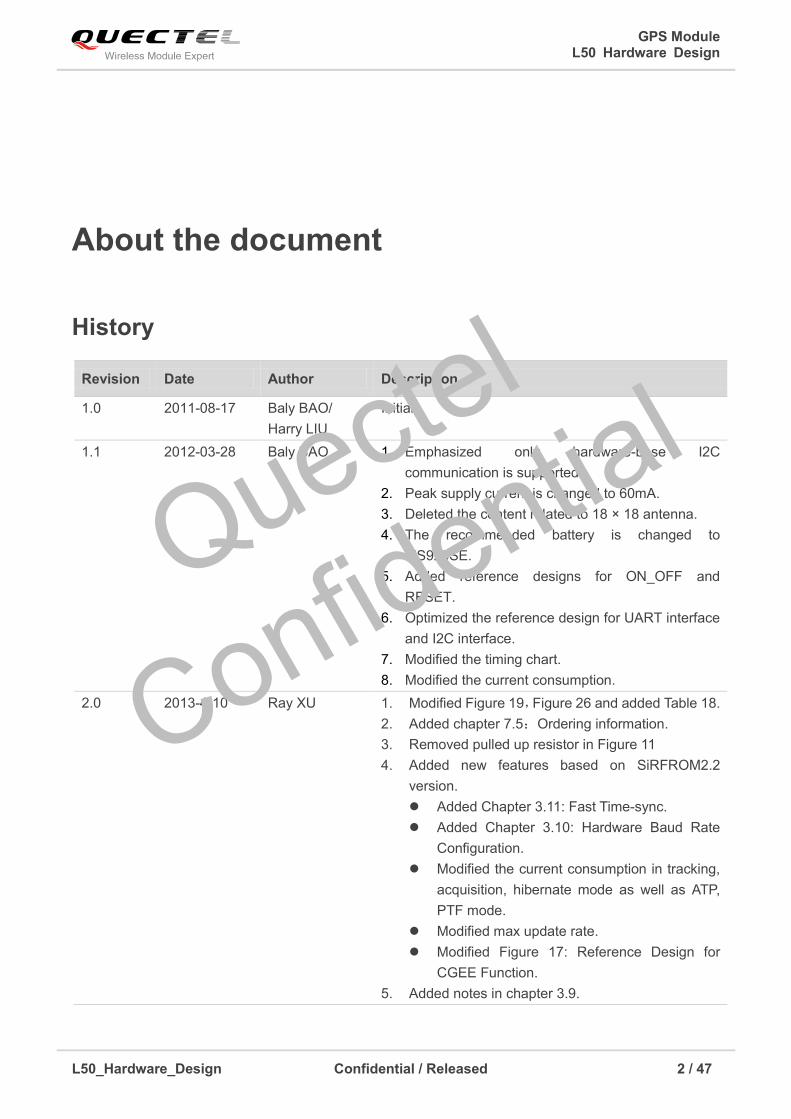
About the document
History
Revision Date Author Description
1.0 2011-08-17 Baly BAO/
Harry LIU
Initial
1.1 2012-03-28 Baly BAO 1. Emphasized only hardware-base I2C
communication is supported.
2. Peak supply current is changed to 60mA.
3. Deleted the content related to 18 × 18 antenna.
4. The recommended battery is changed to
MS920SE.
5. Added reference designs for ON_OFF and
RESET.
6. Optimized the reference design for UART interface
and I2C interface.
7. Modified the timing chart.
8. Modified the current consumption.
2.0 2013-4-10 Ray XU 1. Modified Figure 19,Figure 26 and added Table 18.
2. Added chapter 7.5:Ordering information.
3. Removed pulled up resistor in Figure 11
4. Added new features based on SiRFROM2.2
version.
Added Chapter 3.11: Fast Time-sync.
Added Chapter 3.10: Hardware Baud Rate
Configuration.
Modified the current consumption in tracking,
acquisition, hibernate mode as well as ATP,
PTF mode.
Modified max update rate.
Modified Figure 17: Reference Design for
CGEE Function.
5. Added notes in chapter 3.9.
Quectel
Confidential

GPS Module L50 Hardware Design
L50_Hardware_Design Confidential / Released 3 / 47
Contents
About the document ................................................................................................................................... 2
Contents ....................................................................................................................................................... 3
Table Index ................................................................................................................................................... 5
Figure Index ................................................................................................................................................. 6
1 Introduction .......................................................................................................................................... 7
2 Product Concept .................................................................................................................................. 8
2.1. General Description................................................................................................................... 8
2.2. Key Features ............................................................................................................................. 9
2.3. Functional Diagram ................................................................................................................. 10
2.4. Evaluation Board ..................................................................................................................... 10
2.5. Protocol ................................................................................................................................... 11
3 Application Interface ......................................................................................................................... 12
3.1. General Description................................................................................................................. 12
3.2. Pin Assignment of the Module(Bottom view) ..................................................................... 12
3.3. Pin Description ........................................................................................................................ 13
3.4. Operating Modes ..................................................................................................................... 15
3.5. Power Management ................................................................................................................ 16
3.5.1. VCC Power ..................................................................................................................... 16
3.5.2. VIO/RTC Power.............................................................................................................. 16
3.5.3. Energy Saving Mode ...................................................................................................... 16
3.5.3.1. ATP Mode ............................................................................................................. 16
3.5.3.2. PTF Mode ............................................................................................................. 17
3.5.3.3. Hibernate Mode .................................................................................................... 18
3.6. Power Supply .......................................................................................................................... 19
3.6.1. Power Reference Design ............................................................................................... 19
3.6.2. Battery ............................................................................................................................ 19
3.7. Timing Sequence .................................................................................................................... 21
3.8. Communication Interface ........................................................................................................ 23
3.8.1. UART Interface ............................................................................................................... 24
3.8.2. I2C Interface ................................................................................................................... 25
3.8.3. SPI Interface................................................................................................................... 27
3.9. Assisted GPS .......................................................................................................................... 27
3.10. Hardware Baud Rate Configuration ........................................................................................ 28
3.11. Fast Time-sync ........................................................................................................................ 29
4 Radio Frequency ................................................................................................................................ 30
4.1. Antenna ................................................................................................................................... 30
4.2. PCB Design Guide .................................................................................................................. 31
5 Electrical, Reliability and Radio Characteristics ............................................................................ 33
5.1. Absolute Maximum Ratings .................................................................................................... 33
Quectel
Confidential
GPS Module L50 Hardware Design
L50_Hardware_Design Confidential / Released 4 / 47
5.2. Operating Conditions .............................................................................................................. 33
5.3. Current Consumption .............................................................................................................. 34
5.4. Current Consumption for VIO/RTC domain ............................................................................ 35
5.5. Electro-Static Discharge .......................................................................................................... 35
5.6. Reliability Test ......................................................................................................................... 36
6 Mechanics ........................................................................................................................................... 37
6.1. Mechanical Dimensions of the Module ................................................................................... 37
6.2. Footprint of Recommendation ................................................................................................. 38
6.3. Top View of the Module ........................................................................................................... 39
6.4. Bottom View of the Module ..................................................................................................... 40
7 Manufacture ........................................................................................................................................ 41
7.1. Assembly and Soldering ......................................................................................................... 41
7.2. Moisture Sensitivity ................................................................................................................. 42
7.3. ESD Safe ................................................................................................................................. 42
7.4. Tape and Reel ......................................................................................................................... 43
7.5. Ordering Information ............................................................................................................... 44
8 Appendix Reference .......................................................................................................................... 45
Quectel
Confidential
GPS Module L50 Hardware Design
L50_Hardware_Design Confidential / Released 5 / 47
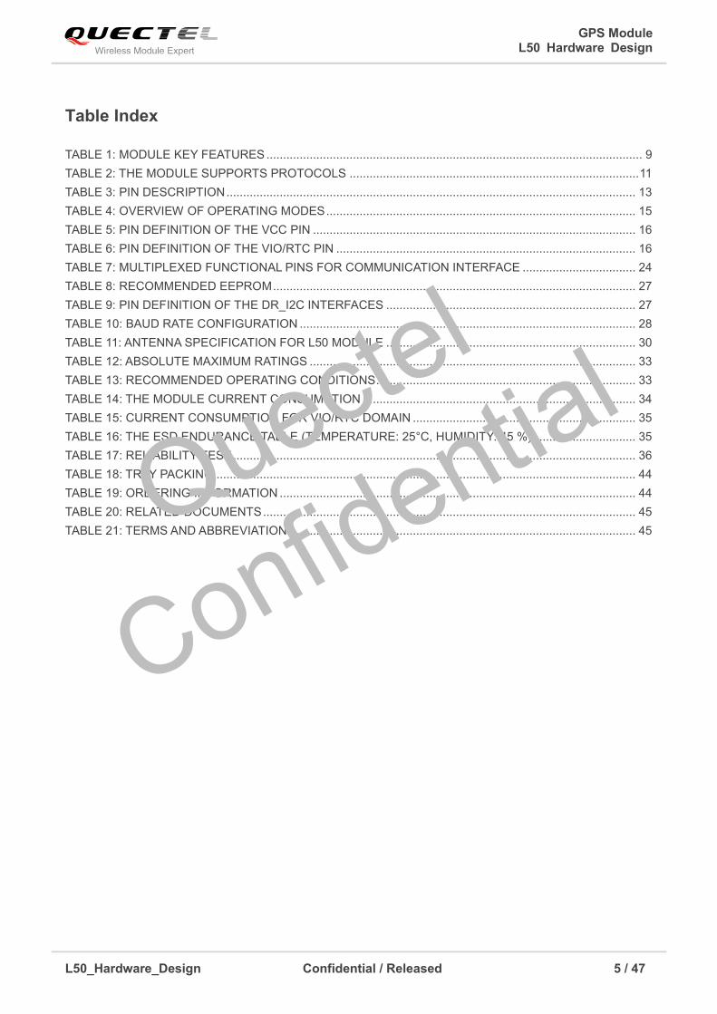
Table Index
TABLE 1: MODULE KEY FEATURES ................................................................................................................. 9
TABLE 2: THE MODULE SUPPORTS PROTOCOLS ....................................................................................... 11
TABLE 3: PIN DESCRIPTION ........................................................................................................................... 13
TABLE 4: OVERVIEW OF OPERATING MODES ............................................................................................. 15
TABLE 5: PIN DEFINITION OF THE VCC PIN ................................................................................................. 16
TABLE 6: PIN DEFINITION OF THE VIO/RTC PIN .......................................................................................... 16
TABLE 7: MULTIPLEXED FUNCTIONAL PINS FOR COMMUNICATION INTERFACE .................................. 24
TABLE 8: RECOMMENDED EEPROM ............................................................................................................. 27
TABLE 9: PIN DEFINITION OF THE DR_I2C INTERFACES ........................................................................... 27
TABLE 10: BAUD RATE CONFIGURATION ..................................................................................................... 28
TABLE 11: ANTENNA SPECIFICATION FOR L50 MODULE ........................................................................... 30
TABLE 12: ABSOLUTE MAXIMUM RATINGS .................................................................................................. 33
TABLE 13: RECOMMENDED OPERATING CONDITIONS .............................................................................. 33
TABLE 14: THE MODULE CURRENT CONSUMPTION .................................................................................. 34
TABLE 15: CURRENT CONSUMPTION FOR VIO/RTC DOMAIN ................................................................... 35
TABLE 16: THE ESD ENDURANCE TABLE (TEMPERATURE: 25°C, HUMIDITY: 45 %) ............................... 35
TABLE 17: RELIABILITY TEST ......................................................................................................................... 36
TABLE 18: TRAY PACKING .............................................................................................................................. 44
TABLE 19: ORDERING INFORMATION ........................................................................................................... 44
TABLE 20: RELATED DOCUMENTS ................................................................................................................ 45
TABLE 21: TERMS AND ABBREVIATIONS ...................................................................................................... 45
Quectel
Confidential

GPS Module L50 Hardware Design
L50_Hardware_Design Confidential / Released 6 / 47
Figure Index
FIGURE 1: MODULE FUNCTIONAL DIAGRAM ............................................................................................... 10
FIGURE 2: BOTTOM VIEW OF THE MODULE ................................................................................................ 12
FIGURE 3: ATP TIMING SEQUENCE ............................................................................................................... 17
FIGURE 4: PTF TIMING SEQUENCE .............................................................................................................. 18
FIGURE 5: POWER DESIGN REFERENCE FOR L50 MODULE .................................................................... 19
FIGURE 6: REFERENCE CHARGING CIRCUIT FOR CHARGEABLE BATTERY .......................................... 20
FIGURE 7: DISCHARGING CHARACTERISTICS OF MS920SE .................................................................... 20
FIGURE 8: TURN ON TIMING SEQUENCE OF MODULE .............................................................................. 21
FIGURE 9: STATE CONVERSION OF MODULE ............................................................................................. 22
FIGURE 10: ON_OFF DESIGN FOR 3V OR 3.3V SYSTEM ............................................................................ 22
FIGURE 11: ON_OFF DESIGN FOR 5V SYSTEM ........................................................................................... 23
FIGURE 12: REFERENCE DESIGN FOR RESET ........................................................................................... 23
FIGURE 13: REFERENCE DESIGN FOR UART INTERFACE ........................................................................ 24
FIGURE 14: RS-232 LEVEL SHIFT CIRCUIT ................................................................................................... 25
FIGURE 15: I2C TIMING SEQUENCE .............................................................................................................. 26
FIGURE 16: REFERENCE DESIGN FOR I2C INTERFACE ............................................................................ 26
FIGURE 17: REFERENCE DESIGN FOR CGEE FUNCTION ......................................................................... 28
FIGURE 18: PATCH ANTENNA TEST RESULT WITH GROUND PLANE 29.5MM×28.5MM .......................... 31
FIGURE 19: L50 MODULE PLACEMENT GUIDE ............................................................................................ 32
FIGURE 20: L50 TOP VIEW AND SIDE VIEW (UNIT: MM) .............................................................................. 37
FIGURE 21: L50 BOTTOM VIEW (UNIT: MM) .................................................................................................. 38
FIGURE 22: FOOTPRINT OF RECOMMENDATION (UNIT: MM) .................................................................... 38
FIGURE 23: TOP VIEW OF MODULE .............................................................................................................. 39
FIGURE 24: BOTTOM VIEW OF MODULE ...................................................................................................... 40
FIGURE 25: RAMP-SOAK-SPIKE-REFLOW OF FURNACE TEMPERATURE ............................................... 41
FIGURE 26: TAPE AND REEL SPECIFICATION (UNIT: MM) .......................................................................... 43
Quectel
Confidential
GPS Module L50 Hardware Design
L50_Hardware_Design Confidential / Released 7 / 47
1 Introduction
This document defines and specifies L50 GPS module. It describes L50 hardware interface and its
external application reference circuits, mechanical size and air interface.
This document can help you quickly understand L50’s interface specifications, electrical and mechanical
characteristics. Associated with application notes, you can use L50 module to design and set up
application easily.
Quectel
Confidential
GPS Module L50 Hardware Design
L50_Hardware_Design Confidential / Released 8 / 47
2 Product Concept
2.1. General Description
L50 is a GPS ROM-based module with embedded GPS patch antenna and features fast acquisition and
tracking with the latest SiRF Star IV ROM2.2 technology. This module provides outstanding GPS
performance in a slim package. Based on an external optional EEPROM which provides capability of
storing ephemeris and downloading patch codes through UART, L50 can support Standalone and A-GPS
(CGEE function). Advanced jamming suppression mechanism and innovative RF architecture, L50
provides a higher level of anti-jamming and ensures maximum GPS performance. The module supports
location, navigation and industrial applications including autonomous GPS C/A, SBAS (WAAS, EGNOS
and QZSS) and A-GPS. Furthermore, a patch antenna has been designed into the L50 module. This will
reduce your design complexity greatly.
L50, in SMD type, can be embedded in your applications via the 24-pin pads with the slim
28×16×3mm package. It provides all hardware interfaces between the module and host board.
The multiplexed communication interface: UART/I2C interface.
The Dead Reckoning I2C interface up to 400Kbps can be used to connect with an external EEPROM
to save ephemeris data for CGEE function and to store patch codes.
The module is RoHS compliant to EU regulation.
Quectel
Confidential

GPS Module L50 Hardware Design
L50_Hardware_Design Confidential / Released 9 / 47
2.2. Key Features
The following table describes the detailed features of L50 module.
Table 1: Module Key Features
Feature Implementation
Power supply Supply voltage: 1.71V – 1.89V typical : 1.8V
Power consumption Acquisition 33 mA @ -130dBm
Tracking 31 mA @ -130dBm
Hibernate 14uA
Receiver Type GPS L1 1575.42MHz C/A Code
48 search channels
Sensitivity(NOTE2) Reacquisition -160dBm
Tracking -163dBm
Acquisition -148dBm
Time-To-First-Fix(NOTE1)
Cold Start (Autonomous) <33s
Warm Start (Autonomous) <33s
Warm Start (With CGEE) 10s typ.
Hot Start (Autonomous) <1s
Horizontal Position Accuracy <2.5 m CEP
Max Update Rate 5Hz 1Hz by default
Accuracy of 1PPS Signal Typical accuracy 500 ns
Time pulse 200ms
Velocity Accuracy Without aid 0.01m/s
Acceleration Accuracy Without aid 0.1m/s²
Dynamic Performance Maximum altitude 18288m
Maximum velocity 514m/s
Acceleration 4 G
Dead Reckoning I2C Interface CGEE
Hardware baud rate configuration
MEMS support (TBD devices)
Standard I2C bus maximum data rate 400kbps
Minimum data rate 100kbps
Communication interface Support multiplexed UART/I2C interface
The output is CMOS 1.8V compatible and the input is 3.6V
tolerant
Temperature range
Normal operation: -40°C ~ +85°C
Storage temperature: -45°C ~ +125°C
Quectel
Confidential

GPS Module L50 Hardware Design
L50_Hardware_Design Confidential / Released 10 / 47
Physical Characteristics Size:
28±0.15 mm×16±0.15 mm×3±0.2mm
Weight: Approx. 4 g
1. TTFF listed in above table is measured in conducted method by 8-star GPS simulator.
2. The sensitivity is measured in conducted method.
2.3. Functional Diagram
The block diagram of L50 is shown in the following figure.
RF Front-End With
Integrated LNA
Fractional-N
Synthesizer
GPS
Engine
ROM
Saw Filter
Power
Management
ARM7
Processor
Peripheral
Controller
RTC
VCC
VIO/RTC
UART/I2C
RESET
EINT0
1PPS
ON/OFF
Optional
EEPROM
For CGEE
DR_I2C
Match
Network
RAM
LNA
PATCH
ANTENNA
Figure 1: Module Functional Diagram
2.4. Evaluation Board
In order to help you to develop applications with L50, Quectel offers an Evaluation Board (EVB) with
appropriate power supply, RS-232 serial port and EEPROM.
For more details, please refer to the document [1].
NOTE
NOTES
Quectel
Confidential
GPS Module L50 Hardware Design
L50_Hardware_Design Confidential / Released 11 / 47
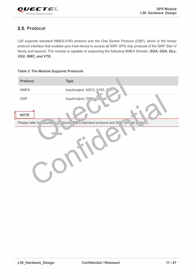
2.5. Protocol
L50 supports standard NMEA-0183 protocol and the One Socket Protocol (OSP), which is the binary
protocol interface that enables your host device to access all SiRF GPS chip products of the SiRF Star IV
family and beyond. The module is capable of supporting the following NMEA formats: GGA, GSA, GLL,
GSV, RMC, and VTG.
Table 2: The Module Supports Protocols
Please refer to document [2] about NMEA standard protocol and SiRF private protocol.
Protocol Type
NMEA Input/output, ASCII, 0183, 3.01
OSP Input/output, OSP protocol
NOTE
Quectel
Confidential
GPS Module L50 Hardware Design
L50_Hardware_Design Confidential / Released 12 / 47
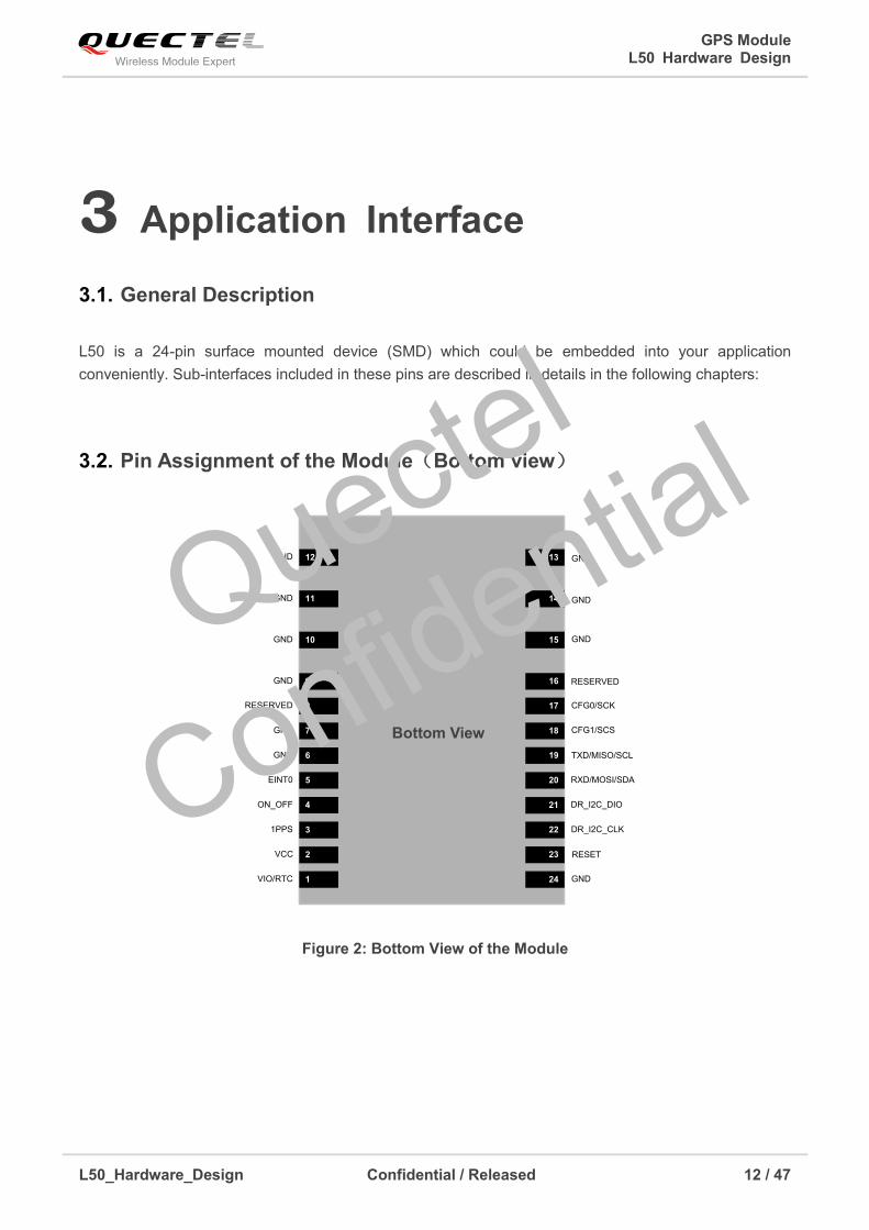
3 Application Interface
3.1. General Description
L50 is a 24-pin surface mounted device (SMD) which could be embedded into your application
conveniently. Sub-interfaces included in these pins are described in details in the following chapters:
3.2. Pin Assignment of the Module(Bottom view)
1
2
3
4
5
6
18
17
16
15
14
13
7
VCC
VIO/RTC
1PPS
ON_OFF
EINT0
GND TXD/MISO/SCL
RXD/MOSI/SDA
DR_I2C_DIO
RESET
GND
8
9
11
12
10
20
19
21
22
23
24
GND
RESERVED
GND
GND
GND
GND GND
GND
GND
RESERVED
CFG1/SCS
DR_I2C_CLK
CFG0/SCK
Figure 2: Bottom View of the Module
Bottom View
Quectel
Confidential

GPS Module L50 Hardware Design
L50_Hardware_Design Confidential / Released 13 / 47
3.3. Pin Description
Table 3: Pin Description
Power Supply
PIN NAME PIN
NO.
I/O DESCRIPTION DC
CHARACTERISTICS
COMMENT
VCC 2 I Supply voltage Vmax= 1.89V
Vmin=1.71V
Vnom=1.8V
Supply current should be no
less than 100mA.
VIO/RTC 1 I RTC and
CMOS I/O
voltage supply
Vmax=1.89V
Vmin=1.71V
Vnom=1.8V
IVIO/RTC=14uA@
Hibernate
mode(VCC=1.8V)
Power supply for RTC and
CMOS I/O. In FULL_ON
mode, make sure both
VIO/RTC and VCC are
simultaneously powered on.
In Hibernate mode, make sure
VIO/RTC is powered on to
keep the data lossless.
General purpose input/output
PIN NAME PIN
NO.
I/O DESCRIPTION DC
CHARACTERISTICS
COMMENT
RESET 23 I External reset
input, active
low
VILmin=0V
VILmax=0.45V
VIHmin=
0.7* VIO/RTC
VIHmax=3.6V
The system reset is provided
by the RTC monitor circuit and
it is active low. If unused,
leave this pin unconnected.
EINT0 5
I External
interrupt input
pin
VILmin=0V
VILmax=0.45V
VIHmin=0.7*VCC
VIHmax=3.6V
Pull this pin down to ground
directly.
ON_OFF 4 I Power control
pin
VILmin=0V
VILmax=0.45V
VIHmin=
0.7* VIO/RTC
VIHmax=3.6
If the pin is pulled down for at
least 1ms and then released,
the module will switch its
working mode between
Hibernate and FULL_ON.
1PPS 3 O One pulse per
second
VOLmin=0V
VOLmax=0.4V
VOHmin=0.75*VCC
1PPS output provides a pulse
signal for time purpose. If
unused, leave this pin
unconnected.
Serial Interface
Quectel
Confidential

GPS Module L50 Hardware Design
L50_Hardware_Design Confidential / Released 14 / 47
PIN NAME PIN
NO.
I/O DESCRIPTION DC
CHARACTERISTICS
COMMENT
DR_I2C_
DIO
21
I/O Dead
Reckoning
I2C data
(SDA)
Baud rate
configurati
on
VOLmax=0.4V
VOHmin=0.75*VCC
VILmin=0V
VILmax=0.45V
VIHmin=0.7*VCC
VIHmax=3.6V
If unused, leave this pin
unconnected.
DR_I2C_
CLK
22 O Dead
Reckoning
I2C
clock(SCL)
Baud rate
configurati
on
VOLmax=0.4V
VOHmin=0.75*VCC
If unused, leave this pin
unconnected.
CFG0/
SCK
17 I Configure Pin 0 VILmin=0V
VILmax=0.45V
VIHmin=0.7*VCC
VIHmax=3.6V
When serial port is configured
as UART, pull up to VCC via a
10k resistor.
CFG1/
SCS
18 I Configure Pin 1 VILmin=0V
VILmax=0.45V
VIHmin=0.7*VCC
VIHmax=3.6V
When serial port is configured
as I2C, pull down to GND via
a 10k resistor.
RXD/
MOSI/
SDA
20 I/O Function
overlay:
UART_RX
UART data
receive
(RXD)
I2C_DIO
I2C data
(SDA)
VOLmax=0.4V
VOHmin=0.75*VCC
VILmin=0V
VILmax=0.45V
VIHmin=0.7*VCC
VIHmax=3.6V
TXD/
MISO/
SCL
19 I/O Function
overlay:
UART_TX
UART data
transmit
(TXD)
I2C_CLK
I2C clock
(SCL)
VOLmax=0.4V
VOHmin=0.75*VCC
VILmin=0V
VILmax=0.45V
VIHmin=0.7*VCC
VIHmax=3.6V
Quectel
Confidential

GPS Module L50 Hardware Design
L50_Hardware_Design Confidential / Released 15 / 47
Others
PIN NAME PIN
NO. I/O DESCRIPTION
DC
CHARACTERISTICS COMMENT
GND
6,7,9,
10,11,
12,
13,14,
15,
24
Ground
Reserved 8,16 Reserved Leave them unconnected.
3.4. Operating Modes
The table below briefly summarizes the various operating modes in the following chapters
Table 4: Overview of Operating Modes
Mode Function
Full on
mode
Acquisition mode
The module starts to search satellite, determine visible satellites and
coarse carrier frequency and code phase of satellite signals. When
the acquisition is done, it switches to tracking mode automatically.
Tracking mode The module refines acquisition’s message, as well as keeps tracking
and demodulating the navigation data from the specific satellites.
Hibernate mode
Hibernate mode means a low power state where only the internal I/O
keeps alive, non-volatile RTC, patch RAM and backup RAM block is
powered on. Other internal blocks like digital baseband and RF are
internally powered off
Quectel
Confidential

GPS Module L50 Hardware Design
L50_Hardware_Design Confidential / Released 16 / 47
3.5. Power Management
There are two power supply pins in L50, VCC and VIO/RTC.
3.5.1. VCC Power
VCC pin supplies power for GPS BB domain and GPS RF domain. The power supply VCC’s current
varies according to the processor load and satellite acquisition. Typical VCC max current is 60 mA. So it is
important that the power is clean and stable. Generally, ensure that the VCC supply ripple voltage meets
the requirement: 54 mV (RMS) max @ f = 0~3MHz and 15 mV (RMS) max @ f > 3 MHz.
Table 5: Pin Definition of the VCC pin
3.5.2. VIO/RTC Power
The VIO/RTC pin supplies power for all RTC domain and CMOS I/O domain, so VIO/RTC should be
powered all the time when the module is running. It ranges from 1.71V to 1.89V. In order to achieve a
better Time To First Fix (TTFF) after VCC powers down, VIO/RTC should be valid all the time. It can
supply power for SRAM memory which contains all the necessary GPS information for quick start-up and
a small amount of user configuration variables.
Table 6: Pin Definition of the VIO/RTC Pin
3.5.3. Energy Saving Mode
3.5.3.1. ATP Mode
Adaptive trickle power (ATP): In this mode, L50 cycles three modes internally to optimize power
consumption. These three modes consist of FULL_ON mode, CPU only mode and standby mode. The
FULL_ON mode lasts typically 300ms to require new ephemeris to get a valid position, and the other two
Name Pin Function
VCC 2 Power supply for GPS BB and RF part
Name Pin Function VIO/RTC 1 Power supply for RTC and CMOS /IO
Quectel
Confidential
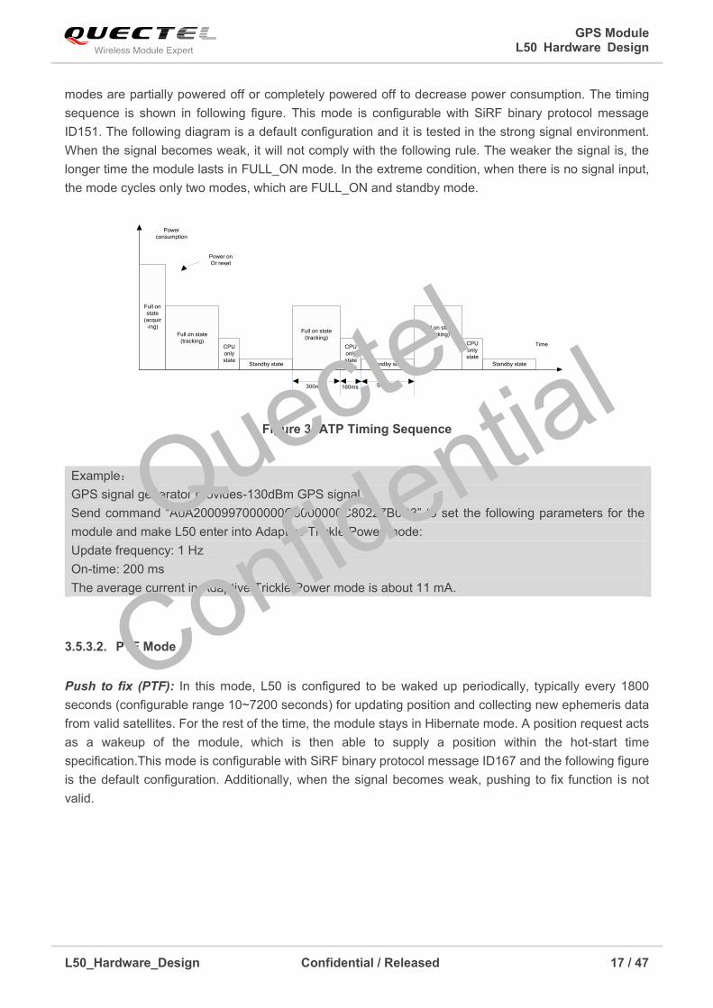
GPS Module L50 Hardware Design
L50_Hardware_Design Confidential / Released 17 / 47
modes are partially powered off or completely powered off to decrease power consumption. The timing
sequence is shown in following figure. This mode is configurable with SiRF binary protocol message
ID151. The following diagram is a default configuration and it is tested in the strong signal environment.
When the signal becomes weak, it will not comply with the following rule. The weaker the signal is, the
longer time the module lasts in FULL_ON mode. In the extreme condition, when there is no signal input,
the mode cycles only two modes, which are FULL_ON and standby mode.
Time
Power
consumption
Full on
state
(acquir
-ing)
Full on state
(tracking)CPU
only
stateStandby state
Full on state
(tracking)
Full on state
(tracking)
CPU
only
stateStandby state
CPU
only
state
Standby state
Power on
Or reset
540ms160ms300ms
Figure 3: ATP Timing Sequence
Example:
GPS signal generator provides-130dBm GPS signal.
Send command “A0A2000997000000C8000000C80227B0B3” to set the following parameters for the
module and make L50 enter into Adaptive Trickle Power mode:
Update frequency: 1 Hz
On-time: 200 ms
The average current in Adaptive Trickle Power mode is about 11 mA.
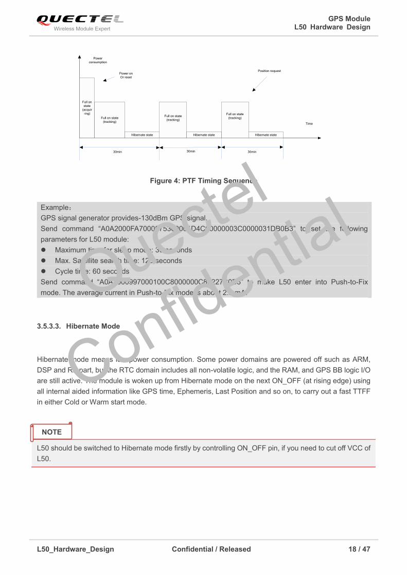
3.5.3.2. PTF Mode
Push to fix (PTF): In this mode, L50 is configured to be waked up periodically, typically every 1800
seconds (configurable range 10~7200 seconds) for updating position and collecting new ephemeris data
from valid satellites. For the rest of the time, the module stays in Hibernate mode. A position request acts
as a wakeup of the module, which is then able to supply a position within the hot-start time
specification.This mode is configurable with SiRF binary protocol message ID167 and the following figure
is the default configuration. Additionally, when the signal becomes weak, pushing to fix function is not
valid.
Quectel
Confidential
GPS Module L50 Hardware Design
L50_Hardware_Design Confidential / Released 18 / 47
Time
Power
consumption
Full on
state
(acquir
-ing)
Full on state
(tracking)
Full on state
(tracking)
Full on state
(tracking)
Hibernate state
Power on
Or reset
Position request
Hibernate state Hibernate state
30min 30min 30min
Figure 4: PTF Timing Sequence
Example:
GPS signal generator provides-130dBm GPS signal.
Send command “A0A2000FA7000075300001D4C00000003C0000031DB0B3” to set the following
parameters for L50 module:
Maximum time for sleep mode: 30 seconds
Max. Satellite search time: 120 seconds
Cycle time: 60 seconds
Send command “A0A2000997000100C8000000C80227B0B3” to make L50 enter into Push-to-Fix
mode. The average current in Push-to-Fix mode is about 2.5 mA.
3.5.3.3. Hibernate Mode
Hibernate mode means low power consumption. Some power domains are powered off such as ARM,
DSP and RF part, but the RTC domain includes all non-volatile logic, and the RAM, and GPS BB logic I/O
are still active. The module is woken up from Hibernate mode on the next ON_OFF (at rising edge) using
all internal aided information like GPS time, Ephemeris, Last Position and so on, to carry out a fast TTFF
in either Cold or Warm start mode.
L50 should be switched to Hibernate mode firstly by controlling ON_OFF pin, if you need to cut off VCC of
L50.
NOTE
Quectel
Confidential
GPS Module L50 Hardware Design
L50_Hardware_Design Confidential / Released 19 / 47
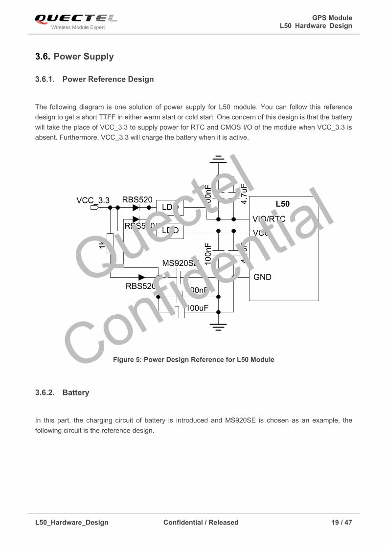
3.6. Power Supply
3.6.1. Power Reference Design
The following diagram is one solution of power supply for L50 module. You can follow this reference
design to get a short TTFF in either warm start or cold start. One concern of this design is that the battery
will take the place of VCC_3.3 to supply power for RTC and CMOS I/O of the module when VCC_3.3 is
absent. Furthermore, VCC_3.3 will charge the battery when it is active.
VIO/RTC
VCC
L50LDO
LDO
VCC_3.3
GND
1K
10
0n
F
4.7
uF
10
0n
F
4.7
uF
100nF
100uF
MS920SE
RBS520
RBS520
RBS520
Figure 5: Power Design Reference for L50 Module
3.6.2. Battery
In this part, the charging circuit of battery is introduced and MS920SE is chosen as an example, the
following circuit is the reference design.
Quectel
Confidential

GPS Module L50 Hardware Design
L50_Hardware_Design Confidential / Released 20 / 47
VCC_3.3
1K
100nF
100uF
MS920SE
RBS520
Figure 6: Reference Charging Circuit for Chargeable Battery
Coin-type rechargeable battery such as MS920SE from Seiko can be used and the schottky diode such
as RB520S30T1G from ON Semiconductor is recommended to be used here for its low voltage drop. The
discharging characteristic of MS920SE is shown in the following figure.
Figure 7: Discharging Characteristics of MS920SE
Quectel
Confidential

GPS Module L50 Hardware Design
L50_Hardware_Design Confidential / Released 21 / 47
3.7. Timing Sequence
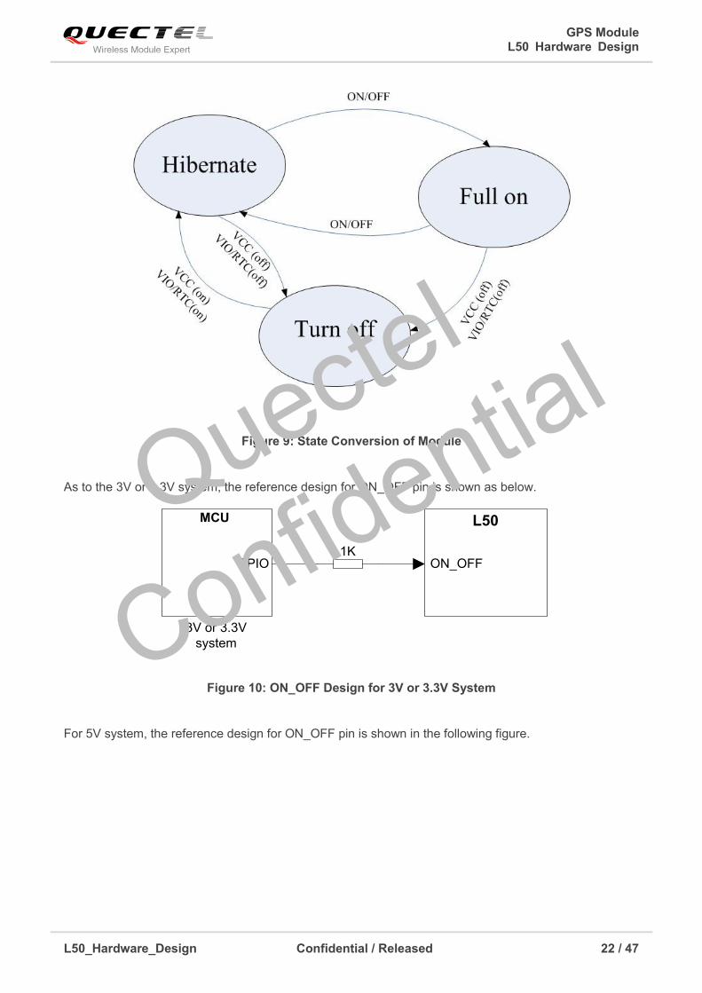
The ON_OFF pin is used to switch the module between FULL_ON mode and Hibernate mode.
L50 integrates internal power on reset circuit with external RESET signal which belongs to VIO/RTC
domain. When VCC and VIO/RTC are supplied simultaneously, the internal power on reset circuit
executes. Normally, external control of RESET is not necessary.
The following diagram is the reference timing sequence. Firstly, VCC and VIO/RTC power on, then a
pulse of wakeup will be generated, after that when ON_OFF is toggled, the module will go into the
FULL_ON mode and the WAKEUP will turn to high level. Next toggling of the ON_OFF will make the
module return to the Hibernate mode. The state conversion is shown in the following figure.
VCC
VIO/RTC
ON/OFF
WAKEUP
UART
Invalid Valid Invalid
(FULL ON)
(Hibernate)(Hibernate)
>1ms
400us
400ms
>1ms
35ms
T>0
>1s
Figure 8: Turn on Timing Sequence of Module
1. If the “ON_OFF” pin is controlled by host controller, a 1KΩ resistor should be inserted between the
GPIO of the controller and “ON_OFF” pin.
2. WAKEUP is an internal signal of L50.
NOTES
Quectel
Confidential
GPS Module L50 Hardware Design
L50_Hardware_Design Confidential / Released 22 / 47
Figure 9: State Conversion of Module
As to the 3V or 3.3V system, the reference design for ON_OFF pin is shown as below.
MCU
ON_OFF
L50
GPIO
3V or 3.3V
system
1K
Figure 10: ON_OFF Design for 3V or 3.3V System
For 5V system, the reference design for ON_OFF pin is shown in the following figure.
Quectel
Confidential
GPS Module L50 Hardware Design
L50_Hardware_Design Confidential / Released 23 / 47
MCU
ON_OFF
L50
GPIO
5V system
4.7K
47
K
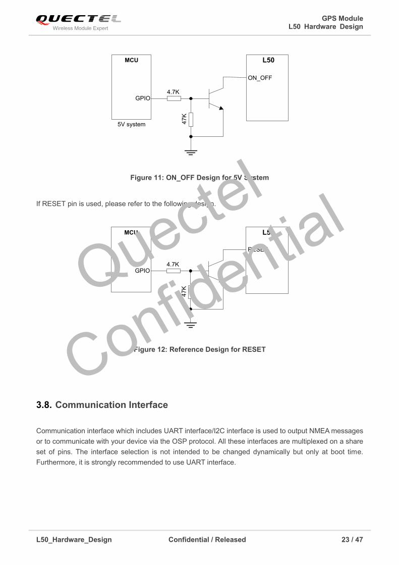
Figure 11: ON_OFF Design for 5V System
If RESET pin is used, please refer to the following design.
MCU
RESET
L50
GPIO4.7K
47
K
Figure 12: Reference Design for RESET
3.8. Communication Interface
Communication interface which includes UART interface/I2C interface is used to output NMEA messages
or to communicate with your device via the OSP protocol. All these interfaces are multiplexed on a share
set of pins. The interface selection is not intended to be changed dynamically but only at boot time.
Furthermore, it is strongly recommended to use UART interface.
Quectel
Confidential
GPS Module L50 Hardware Design
L50_Hardware_Design Confidential / Released 24 / 47
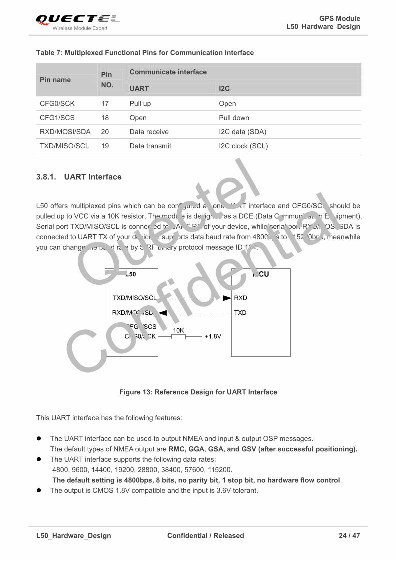
Table 7: Multiplexed Functional Pins for Communication Interface
Pin name Pin
NO.
Communicate interface
UART I2C
CFG0/SCK 17 Pull up Open
CFG1/SCS 18 Open Pull down
RXD/MOSI/SDA 20 Data receive I2C data (SDA)
TXD/MISO/SCL 19 Data transmit I2C clock (SCL)
3.8.1. UART Interface
L50 offers multiplexed pins which can be configured as one UART interface and CFG0/SCK should be
pulled up to VCC via a 10K resistor. The module is designed as a DCE (Data Communication Equipment).
Serial port TXD/MISO/SCL is connected to UART RX of your device, while serial port RXD/MOSI/SDA is
connected to UART TX of your device. It supports data baud rate from 4800bps to 115200bps, meanwhile
you can change the baud rate by SIRF binary protocol message ID 134.
TXD/MISO/SCL
RXD/MOSI/SDA
L50
RXD
TXD
MCU
CFG1/SCS
CFG0/SCK10K
+1.8V
Figure 13: Reference Design for UART Interface
This UART interface has the following features:
The UART interface can be used to output NMEA and input & output OSP messages.
The default types of NMEA output are RMC, GGA, GSA, and GSV (after successful positioning).
The UART interface supports the following data rates:
4800, 9600, 14400, 19200, 28800, 38400, 57600, 115200.
The default setting is 4800bps, 8 bits, no parity bit, 1 stop bit, no hardware flow control.
The output is CMOS 1.8V compatible and the input is 3.6V tolerant.
Quectel
Confidential

GPS Module L50 Hardware Design
L50_Hardware_Design Confidential / Released 25 / 47
It is strongly recommended that the UART interface is used to output NMEA message to serial port of host
processor.
The UART interface does not support the RS-232 level. It supports the TTL/CMOS level. If the module’s
UART interface is connected to the UART interface of a computer, it is necessary to insert a level shift
circuit between the module and the computer. Please refer to the following figure.
Figure 14: RS-232 Level Shift Circuit
3.8.2. I2C Interface
L50 provides multiplex function via TXD/MISO/SCL, RXD/MOSI/SDA and CFG1/SCS to construct I2C
interface. Communication interface is configured as I2C by pulling down CFG1/SCS. The default mode is
master mode. It is important that you must pull up these two pins via 2.2K resistor for the OC/OD interface.
Otherwise, there is no signal output. In addition, only hardware-based I2C communication is supported.
This interface acts as a master when it outputs NMEA data, while it is a slave when it receives
commands.
This I2C interface has the following features:
Operate up to 400kbps.
Support Multi-master I2C mode by default.
NOTE
Quectel
Confidential

GPS Module L50 Hardware Design
L50_Hardware_Design Confidential / Released 26 / 47
Default I2C address values are RX: 0x60, TX: 0x62.
The following figure is the I2C timing sequence.
Figure 15: I2C Timing Sequence
The following circuit is an example of connection.
TXD/MISO/SCL
RXD/MOSI/SDA
L50
SCL
SDA
MCU
CFG1/SCS
CFG0/SCK
10K
3V or 3.3V system
VCCMCU_VCC
MCU_VCC
Figure 16: Reference Design for I2C Interface
The above figure only shows the reference design of I2C interface for the 3V or 3.3V system. For 5V
system, a level shifter should be used.
NOTE
Quectel
Confidential

GPS Module L50 Hardware Design
L50_Hardware_Design Confidential / Released 27 / 47
3.8.3. SPI Interface
The Serial Peripheral Interface (SPI) provides access to a flexible, full-duplex synchronous serial bus.
However, L50 does not support SPI at present.
3.9. Assisted GPS
By supplying aided information like ephemeris, almanac, rough last position, time and satellite status,
A-GPS can help improve TTFF and the acquisition sensitivity of the GPS receiver.
L50 supports one kind of A-GPS called Client Generated Extended Ephemeris (CGEE) which ensures
fast TTFF up to 3 days. The CGEE data is generated internally from satellite ephemeris as a background
task, and then L50 collects ephemeris from as many satellites as possible before entering Hibernate
mode.
The CGEE functionality requires that VIO/RTC power supply is kept active all the time and an external
1Mbit EEPROM connected to DR_I2C bus for CGEE data storage. The recommended EEPROMs are in
the following table and they are verified.
Table 8: Recommended EEPROM
Manufacturer Part Number ST M24M01
Seiko Instruments Inc. S-24CM01C
Atmel AT24C1024B
1. The part number which we recommend is a series part number, please get more details from the
datasheet such as operation voltage and package.
2. [email protected] only supports 1.8V EEPROM.
3. DR_I2C_DIO and DR_I2C_CLK pins have been pulled up to VCC internally.
Table 9: Pin Definition of the DR_I2C Interfaces
Interface Name Pin Function
Dead Reckoning I2C Interface DR_I2C_DIO 21 I2C data (SDA)
NOTES
Quectel
Confidential
GPS Module L50 Hardware Design
L50_Hardware_Design Confidential / Released 28 / 47
DR_I2C_CLK 22 I2C clock (SCL)
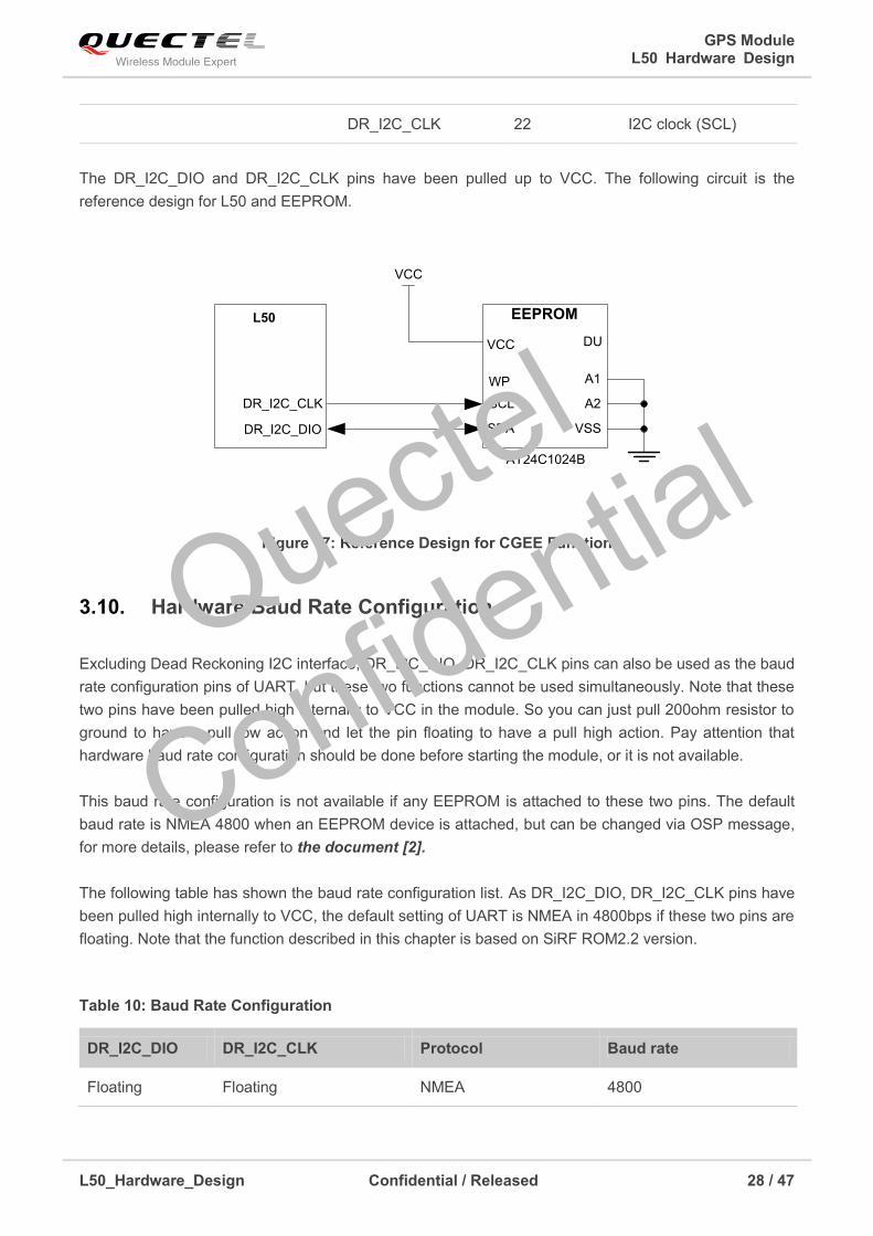
The DR_I2C_DIO and DR_I2C_CLK pins have been pulled up to VCC. The following circuit is the
reference design for L50 and EEPROM.
DR_I2C_CLK
DR_I2C_DIO
L50
SCL
SDA
EEPROM
AT24C1024B
VCC
VCC
WP
VSS
A1
A2
DU
Figure 17: Reference Design for CGEE Function
3.10. Hardware Baud Rate Configuration
Excluding Dead Reckoning I2C interface, DR_I2C_DIO, DR_I2C_CLK pins can also be used as the baud
rate configuration pins of UART, but these two functions cannot be used simultaneously. Note that these
two pins have been pulled high internally to VCC in the module. So you can just pull 200ohm resistor to
ground to have a pull low action and let the pin floating to have a pull high action. Pay attention that
hardware baud rate configuration should be done before starting the module, or it is not available.
This baud rate configuration is not available if any EEPROM is attached to these two pins. The default
baud rate is NMEA 4800 when an EEPROM device is attached, but can be changed via OSP message,
for more details, please refer to the document [2].
The following table has shown the baud rate configuration list. As DR_I2C_DIO, DR_I2C_CLK pins have
been pulled high internally to VCC, the default setting of UART is NMEA in 4800bps if these two pins are
floating. Note that the function described in this chapter is based on SiRF ROM2.2 version.
Table 10: Baud Rate Configuration
DR_I2C_DIO DR_I2C_CLK Protocol Baud rate
Floating Floating NMEA 4800
Quectel
Confidential
GPS Module L50 Hardware Design
L50_Hardware_Design Confidential / Released 29 / 47
Floating Pull low NMEA 9600
Pull low Floating NMEA 38400
3.11. Fast Time-sync
L50 provides Fast time-sync function for special application to reduce power consumption. These special
applications include watches and clocks for UTC time. It uses technique that limits how many message
the satellite navigation must be observed before it declares the correct time. Due to this technique, the
module will find the time very quickly compared to normal operation. It is about 6 seconds to get the UTC
time in the condition of one visible satellite with C/N value bigger than 23 in static states. You can turn off
the module immediately once the UTC time is got to save power consumption. This function is disabled by
default and it can be enabled by OSP Message ID 136, for more details, please refer to the document
[2].
Quectel
Confidential

GPS Module L50 Hardware Design
L50_Hardware_Design Confidential / Released 30 / 47
4 Radio Frequency
L50 receives L1 band signal from GPS satellites at a nominal frequency of 1575.42MHz. It is an ultra slim
module with embedded 15.0×15.0×2.0 mm patch antenna. Alongside highest reliability and quality of
patch antenna, L50 also offers 48 PRN channels, which allows the module to acquire and track satellites
in the shortest time, even at a very low signal level.
4.1. Antenna
The quality of the embedded GPS antenna is crucial to the overall sensitivity of the GPS system. L50
offers an on-module patch antenna. A 15.0×15.0×2.0mm patch antenna is chosen for reducing product
size. This antenna is specially designed for satellite reception applications. And it has excellent stability
and sensitivity to consistently provide high signal reception efficiency. The specification of the antenna
used by L50 is described in following table.
Table 11: Antenna Specification for L50 Module
Antenna
type Parameter Specification Notes
Patch
Antenna
Size 15.0×15.0×2.0mm
Range of receiving
Frequency 1575.42MHz±1.023MHz
Impendence 50 Ohm
Band Width 10MHz minimum Return Loss ≦-10dB
Frequency Temperature
Coefficient (TF) 0±20ppm/°C -40°C-150°C
Polarization RHCP Right Hand Circular Polarization
Gain at Zenith 1.0dBi typ
Centre frequency VSWR 1.5 max
Axial ratio 3 dB max
Quectel
Confidential
GPS Module L50 Hardware Design
L50_Hardware_Design Confidential / Released 31 / 47
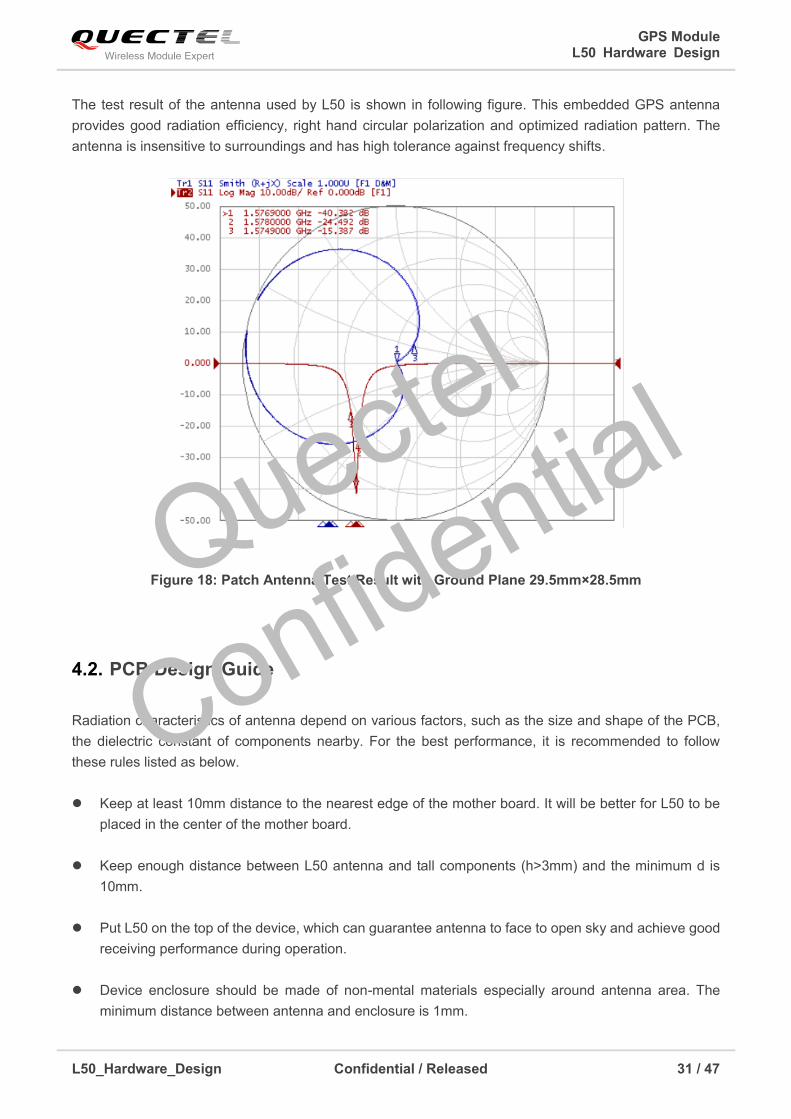
The test result of the antenna used by L50 is shown in following figure. This embedded GPS antenna
provides good radiation efficiency, right hand circular polarization and optimized radiation pattern. The
antenna is insensitive to surroundings and has high tolerance against frequency shifts.
Figure 18: Patch Antenna Test Result with Ground Plane 29.5mm×28.5mm
4.2. PCB Design Guide
Radiation characteristics of antenna depend on various factors, such as the size and shape of the PCB,
the dielectric constant of components nearby. For the best performance, it is recommended to follow
these rules listed as below.
Keep at least 10mm distance to the nearest edge of the mother board. It will be better for L50 to be
placed in the center of the mother board.
Keep enough distance between L50 antenna and tall components (h>3mm) and the minimum d is
10mm.
Put L50 on the top of the device, which can guarantee antenna to face to open sky and achieve good
receiving performance during operation.
Device enclosure should be made of non-mental materials especially around antenna area. The
minimum distance between antenna and enclosure is 1mm.
Quectel
Confidential
GPS Module L50 Hardware Design
L50_Hardware_Design Confidential / Released 32 / 47
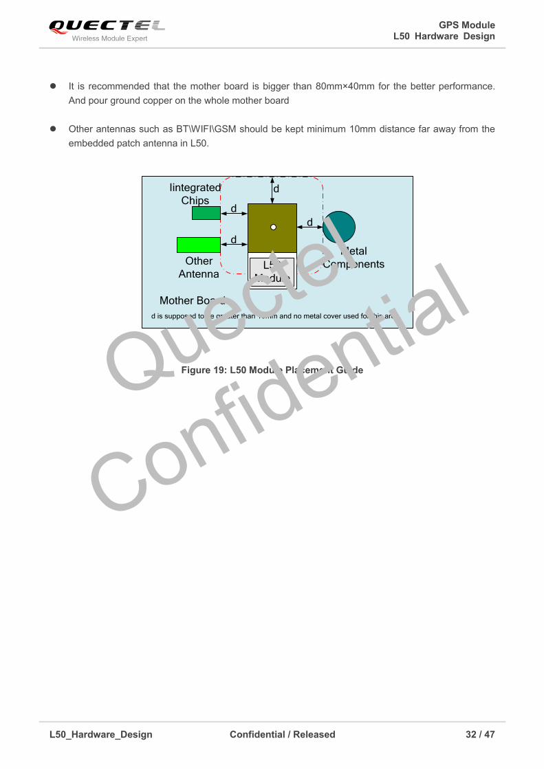
It is recommended that the mother board is bigger than 80mm×40mm for the better performance.
And pour ground copper on the whole mother board
Other antennas such as BT\WIFI\GSM should be kept minimum 10mm distance far away from the
embedded patch antenna in L50.
L50
Module
Mother Board
Iintegrated
Chips
Metal
Components Other
Antenna
d
d
d
d
d is supposed to be greater than 10mm and no metal cover used for this area.
Figure 19: L50 Module Placement Guide
Quectel
Confidential

GPS Module L50 Hardware Design
L50_Hardware_Design Confidential / Released 33 / 47
5 Electrical, Reliability and Radio
Characteristics
5.1. Absolute Maximum Ratings
Absolute maximum rating for power supply and voltage on digital pins of the module are listed in the
following table
Table 12: Absolute Maximum Ratings
Parameter Min Max Unit
Power supply voltage (VCC) -0.3 2 V
Backup battery voltage (VIO/RTC) -0.3 2 V
Input voltage at digital pins -0.5 3.6 V
Storage temperature range -45 125 °C
Stressing the device beyond the “Absolute Maximum Ratings” may cause permanent damage. These are
stress ratings only. The product is not protected against over voltage or reversed voltage. If necessary,
voltage spikes exceeding the power supply voltage specification, given in table above, must be limited to
values within the specified boundaries by using appropriate protection diodes
5.2. Operating Conditions
Table 13: Recommended Operating Conditions
Parameter Description Conditions Min Typ Max Unit
VCC Supply voltage Voltage must stay 1.71 1.8 1.89 V
NOTE
Quectel
Confidential
GPS Module L50 Hardware Design
L50_Hardware_Design Confidential / Released 34 / 47
within the min/max
values, including
voltage drop, ripple,
and spikes.
IVCC Peak supply current VCC=1.8V@-148dBm - - 60 mA
VIO/RTC Backup voltage
supply
1.71 1.8 1.89 V
IVIO/RTC Backup battery
current
VIO/RTC=1.8V in
Hibernate mode
- 14 - uA
TOPR Normal Operating
temperature
-40 25 85 °C
Operation beyond the "Operating Conditions" is not recommended and extended exposure beyond the
"Operating Conditions" may affect device reliability.
5.3. Current Consumption
Table 14: The Module Current Consumption
I total=IVCC+IVIO/RTC
Parameter Condition Min Typ Max Unit
I total Acquisition Open sky @-130dBm - 33 - mA
I total Tracking Open sky@-130dBm - 31 - mA
I total Hibernate VIO/RTC=VCC=1.8V - 14 - uA
NOTE
NOTE
Quectel
Confidential

GPS Module L50 Hardware Design
L50_Hardware_Design Confidential / Released 35 / 47
5.4. Current Consumption for VIO/RTC domain
Table 15: Current Consumption for VIO/RTC Domain
5.5. Electro-Static Discharge
L50 module has excellent ESD performance, because every pin is protected by a transient voltage
suppressor (TVS). However, ESD protection precautions should still be emphasized. Proper ESD
handing and packaging procedures must be applied throughout the processing, handing and operation of
any application.
The ESD bearing capability of the module is listed in the following table.
Table 16: The ESD Endurance Table (Temperature: 25°C, Humidity: 45 %)
Pin Contact discharge Air discharge
VCC, GND,
Patch antenna ±5KV ±10KV
Others ±4KV ±8KV
Parameter Condition Min Type Max Unit
IVIO/RTC
In FULL_ON mode, VCC =
1.8V. 980 uA
Enter into FULL_ON mode
firstly and then turn off VCC. 800 uA
In Hibernate mode, VCC =
1.8V. 14 uA
Enter into Hibernate mode
firstly and then turn off VCC. 14 uA
Quectel
Confidential

GPS Module L50 Hardware Design
L50_Hardware_Design Confidential / Released 36 / 47
5.6. Reliability Test
Table 17: Reliability Test
Test Item Condition Standard
Thermal shock -30°C...+80°C, 144 cycles GB/T 2423.22-2002 Test Na
IEC 68-2-14 Na
Damp heat, cyclic +55°C; >90% Rh 6 cycles for 144 hours IEC 68-2-30 Db Test
Vibration shock 5~20Hz,0.96m
2/s
3;20~500Hz,0.96m
2/s
3-
3dB/oct, 1hour/axis; no function
2423.13-1997 Test Fdb
IEC 68-2-36 Fdb Test
Heat test 85°C, 2 hours, Operational GB/T 2423.1-2001 Ab
IEC 68-2-1 Test
Cold test -40°C, 2 hours, Operational GB/T 2423.1-2001 Ab
IEC 68-2-1 Test
Heat soak 90°C, 72 hours, Non-Operational GB/T 2423.2-2001 Bb
IEC 68-2-2 Test B
Cold soak -45°C, 72 hours, Non-Operational GB/T 2423.1-2001 A
IEC 68-2-1 Test
Quectel
Confidential

GPS Module L50 Hardware Design
L50_Hardware_Design Confidential / Released 37 / 47
6 Mechanics
This chapter describes the mechanical dimensions of the module.
6.1. Mechanical Dimensions of the Module
Figure 20: L50 Top View and Side View (Unit: mm)
Quectel
Confidential
GPS Module L50 Hardware Design
L50_Hardware_Design Confidential / Released 38 / 47
Figure 21: L50 Bottom View (Unit: mm)
6.2. Footprint of Recommendation
Figure 22: Footprint of Recommendation (Unit: mm)
1
12 13
24
Quectel
Confidential
GPS Module L50 Hardware Design
L50_Hardware_Design Confidential / Released 39 / 47
6.3. Top View of the Module
Figure 23: Top View of Module
1
12 13
24
Quectel
Confidential

GPS Module L50 Hardware Design
L50_Hardware_Design Confidential / Released 40 / 47
6.4. Bottom View of the Module
Figure 24: Bottom View of Module
1
12
24
13
Quectel
Confidential

GPS Module L50 Hardware Design
L50_Hardware_Design Confidential / Released 41 / 47
7 Manufacture
7.1. Assembly and Soldering
L50 is intended for SMT assembly and soldering in a Pb-free reflow process on the top side of the PCB. It
is suggested that the minimum height of solder paste stencil is 130um to ensure sufficient solder volume.
Pad openings of paste mask can be increased to ensure proper soldering and solder wetting over pads. It
is suggested that peak reflow temperature is 235~245ºC (for SnAg3.0Cu0.5 alloy). Absolute max reflow
temperature is 260ºC. To avoid damage to the module when it is repeatedly heated, it is suggested that
the module should be mounted after the first panel has been reflowed. The following picture is the actual
diagram which we have operated.
Time(s)
50 100 150 200 250 300
50
100
150
200
250
160℃
200℃
217
0
70s~120s
40s~60s
Between 1~3℃/S
Preheat Heating Cooling℃
s
Liquids Temperature
Figure 25: Ramp-soak-spike-reflow of Furnace Temperature
Quectel
Confidential
GPS Module L50 Hardware Design
L50_Hardware_Design Confidential / Released 42 / 47
7.2. Moisture Sensitivity
L50 is sensitive to moisture absorption. To prevent L50 from permanent damage during reflow soldering,
baking before reflow is required in following cases:
Humidity indicator card: At least one circular indicator is no longer blue.
The seal is opened and the module is exposed to excessive humidity.
L50 should be baked for 192 hours at temperature 40℃±5℃/-0℃ and <5% RH in low-temperature
containers, or 24 hours at temperature 125℃±5℃ in high-temperature containers. Care should be taken
that plastic tray is not heat resistant. L50 should be taken out before pre-heating, otherwise, the tray may
be damaged by high temperature heating.
7.3. ESD Safe
L50 module is an ESD sensitive device and should be careful to handle.
Quectel
Confidential

GPS Module L50 Hardware Design
L50_Hardware_Design Confidential / Released 43 / 47
7.4. Tape and Reel
5
direction
Figure 26: Tape and Reel Specification (Unit: mm)
Quectel
Confidential
GPS Module L50 Hardware Design
L50_Hardware_Design Confidential / Released 44 / 47
Table 18: Tray Packing
Model Name MOQ for MP Minimum Package:250pcs Minimum Package ×
4=1000pcs
L50 250pcs
Size: 370×350×56mm
N.W: 1.000kg
G.W: 1.723kg
Size: 380×250×365mm
N.W: 4.000kg
G.W: 7.370kg
7.5. Ordering Information
Table 19: Ordering Information
Model Name Product Number Ordering Code
[email protected] S2-W1111 L50B-S44
Quectel
Confidential

GPS Module L50 Hardware Design
L50_Hardware_Design Confidential / Released 45 / 47
8 Appendix Reference
Table 20: Related Documents
SN Document name Remark
[1] L50_EVB _User_Guide L50 EVB User Guide
[2] L50_GPS_Protocol L50 GPS Protocol Specification
[3] SIRF_AGPS_Application_Note SIRF Platform A-GPS Application Note
Table 21: Terms and Abbreviations
Abbreviation Description
CGEE Client Generated Extended Ephemeris
CPU Center processing unit
EMC Electromagnetic Compatibility
ESD Electrostatic Discharge
EGNOS European Geostationary Navigation Overlay Service
GPS Global Positioning System
GNSS Global Navigation Satellite System
GGA GPS Fix Data
GLL Geographic Position – Latitude/Longitude
GSA GNSS DOP and Active Satellites
GSV GNSS Satellites in View
HDOP Horizontal Dilution of Precision
IC Integrated Circuit
Quectel
Confidential
GPS Module L50 Hardware Design
L50_Hardware_Design Confidential / Released 46 / 47
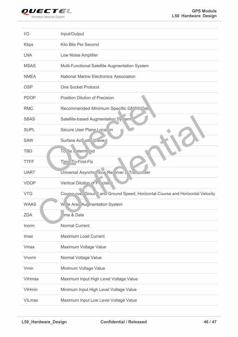
I/O Input/Output
Kbps Kilo Bits Per Second
LNA Low Noise Amplifier
MSAS Multi-Functional Satellite Augmentation System
NMEA National Marine Electronics Association
OSP One Socket Protocol
PDOP Position Dilution of Precision
RMC Recommended Minimum Specific GNSS Data
SBAS Satellite-based Augmentation System
SUPL Secure User Plane Location
SAW Surface Acoustic Wave
TBD To Be Determined
TTFF Time-To-First-Fix
UART Universal Asynchronous Receiver & Transmitter
VDOP Vertical Dilution of Precision
VTG Course over Ground and Ground Speed, Horizontal Course and Horizontal Velocity
WAAS Wide Area Augmentation System
ZDA Time & Date
Inorm Normal Current
Imax Maximum Load Current
Vmax Maximum Voltage Value
Vnorm Normal Voltage Value
Vmin Minimum Voltage Value
VIHmax Maximum Input High Level Voltage Value
VIHmin Minimum Input High Level Voltage Value
VILmax Maximum Input Low Level Voltage Value
Quectel
Confidential

GPS Module L50 Hardware Design
L50_Hardware_Design Confidential / Released 47 / 47
VILmin Minimum Input Low Level Voltage Value
VImax Absolute Maximum Input Voltage Value
VImin Absolute Minimum Input Voltage Value
VOHmax Maximum Output High Level Voltage Value
VOHmin Minimum Output High Level Voltage Value
VOLmax Maximum Output Low Level Voltage Value
VOLmin Minimum Output Low Level Voltage Value
Quectel
Confidential